

Page 1

UM11524
First Field Verification Tool User manual
Rev. 1 — 24 February 2021 User manual
Document information
Information Content
Keywords SEN-SPI-BOX, FFV Tool
Abstract FFV Tool User manual
Page 2

NXP Semiconductors
Revision history
Rev Date Description
1 20210224 • Initial release
UM11524
First Field Verification Tool User manual
UM11524 All information provided in this document is subject to legal disclaimers. © NXP B.V. 2021. All rights reserved.
User manual Rev. 1 — 24 February 2021
2 / 34
Page 3
NXP Semiconductors
1 Introduction
This document describes how to use the SEN-SPI-BOX kit for NXP automotive sensor
evaluation with the “NXP First Field Verification Tool” software.
The intent of this document is to get started, from the hardware configuration to the
software manipulation, in order to communicate with NXP sensors and get interactive
data.
UM11524
First Field Verification Tool User manual
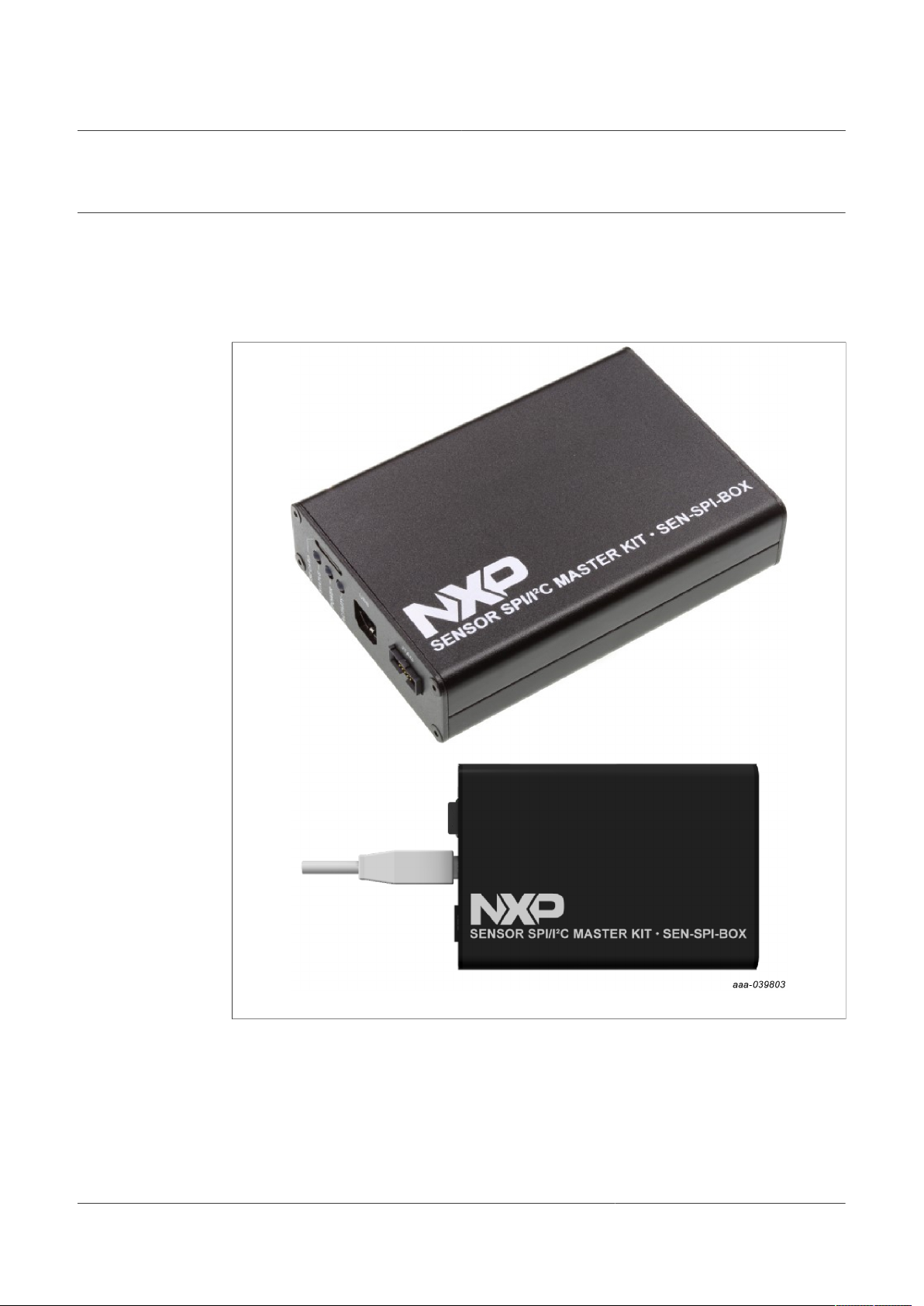
Figure 1. NXP Sensor SPI/I2C Master Kit - SEN-SPI-BOX
UM11524 All information provided in this document is subject to legal disclaimers. © NXP B.V. 2021. All rights reserved.
User manual Rev. 1 — 24 February 2021
3 / 34
Page 4
NXP Semiconductors
2 Getting started
2.1 Kit contents/packing list
UM11524
First Field Verification Tool User manual
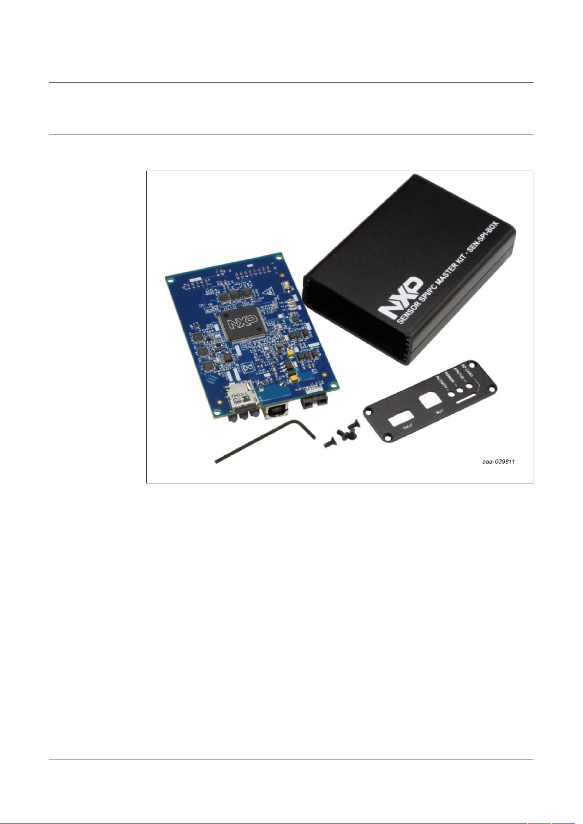
Figure 2. SEN-SPI-BOX kit contents
The SEN-SPI-BOX evaluation board contains:
• One Sensor SPI Master Kit (SEN-SPI-BOX)
• One USB Type A USB cable
• One NXP MDI ribbon cable (16-pin)
• One Beagle ribbon cable (10-pin)
• One debug cable
• One 8 GB microSD card
• One microSD to PC adapter
If DSI3 or PSI5 protocol is required, a SEN-DSI3-ADAPTER and a SEN-PSI5-ADAPTER
may be ordered separately.
SEN-xxxx-ADAPTER kit contains:
• One SEN-xxxx-ADAPTER
• Two, 2-wire twisted cables
UM11524 All information provided in this document is subject to legal disclaimers. © NXP B.V. 2021. All rights reserved.
User manual Rev. 1 — 24 February 2021
4 / 34
Page 5
NXP Semiconductors
2.2 Finding kit resources and information on the NXP website
NXP Semiconductors provides online resources for this evaluation board and supported
devices on http://www.nxp.com. The information page for the SEN-SPI-BOX evaluation
board is at http://nxp.com/SEN-SPI-BOX. The information page provides overview
information, documentation, software and tools, parametrics, ordering information and
a Getting Started tab. The Getting Started tab provides quick-reference information
applicable to using the SEN-SPI-BOX evaluation board, including the downloadable
assets referenced in this document.
3 Hardware description
The NXP SEN-SPI-BOX kit provides a full-solution of built-in functionalities to
communicate with any SPI/I²C sensor. The kit graphs real-time data, executes custom
scripts and verifies sensor status. The board is a generic SPI/I²C evaluation board,
compatible with some of the NXP sensor families such as FXLS9xxxx automotive digital
accelerometers. The list of compatible sensors is non-exhaustive and may evolve in the
future.
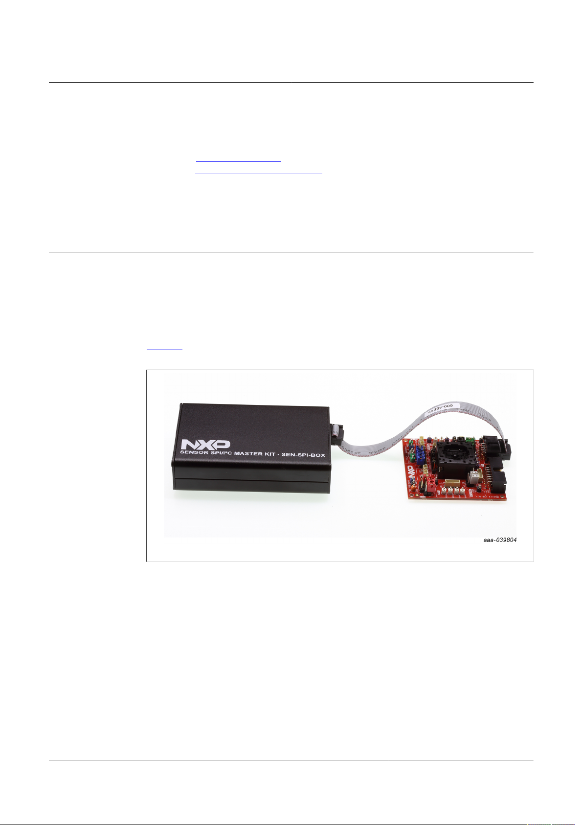
Figure 3 shows how to couple the SEN-SPI-BOX with a SEN-GEN6-SKT board for the
FXLS9xxxx evaluation.
UM11524
First Field Verification Tool User manual
Figure 3. Attaching the SEN-GEN6-SKT board to the SEN-SPI-BOX
3.1 Kit overview
The kit contains an NXP SEN-SPI-BOX evaluation board, three different cables
compatible with dedicated NXP sensor boards, a microSD card for built-in boot loading
capability, and a USB Type-B cable to connect the kit to a computer.
The kit is powered by an NXP Kinetis® K64F Cortex M4 Microcontroller.
UM11524 All information provided in this document is subject to legal disclaimers. © NXP B.V. 2021. All rights reserved.
User manual Rev. 1 — 24 February 2021
5 / 34
Page 6
NXP Semiconductors
Figure 4. SEN-SPI-BOX overview
UM11524
First Field Verification Tool User manual
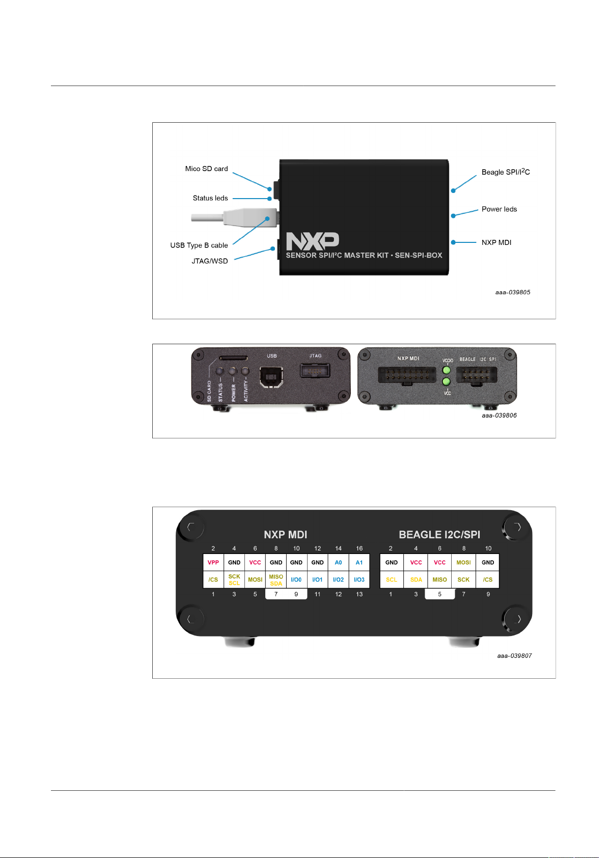
Figure 5. SEN-SPI-BOX interfaces
3.2 Pinout
The NXP MDI (16-pin) and Beagle (10-pin) connectors can be used with their own
dedicated ribbon cable or with breadboard jumper wires.
Figure 6. NXP MDI and Beagle connector pinout
UM11524 All information provided in this document is subject to legal disclaimers. © NXP B.V. 2021. All rights reserved.
User manual Rev. 1 — 24 February 2021
6 / 34
Page 7
NXP Semiconductors
aaa- 0398 35
10
9
8
7
6
5
4
3
2
1
GND
/CS
MOSI
SCK
VCC
MISO
VCC
SDA
SCL
GND
3.2.1 NXP MDI connector
Table 1. NXP MDI connector pinout
3.2.2 Beagle connector
UM11524
First Field Verification Tool User manual
Pin Label Description
6 VCC Power supply: off, 3.3 V or 5 V
2 VPP High-voltage supply: off, 10.5 V or 13.5 V
4,8,10,12 GND Ground
1 /CS SPI chip select
3 SCK/SCL SPI serial clock / I²C serial clock
5 MOSI SPI output
7 MISO/SDA SPI input / I²C serial data
9, 11, 13, 15 I/Ox Configurable input/output
14, 16 Ax Analog input
Table 2. Beagle connector pinout
Pin Label Description
4, 6 VCC Power supply: off, 3.3 V or 5 V
2, 10 GND Ground
9 /CS SPI chip select
7 SCK SPI serial clock
8 MOSI SPI output
5 MISO SPI input
1 SCL I²C serial clock
3 SDA I²C serial data
3.2.3 Beagle debug cable
To directly connect any sensor, use the debug cable (to be plugged into the Beagle
connector).
Figure 7 identifies the debug cable pinout connections.
UM11524 All information provided in this document is subject to legal disclaimers. © NXP B.V. 2021. All rights reserved.
User manual Rev. 1 — 24 February 2021
Figure 7. Debug cable pinouts
7 / 34
Page 8
NXP Semiconductors
3.3 LED indicators
3.3.1 Rear view
Figure 8. Status indicators
• Status: Blinks green if running, if red, something is wrong
• Power: Red when board is powered
• Activity: Fast blink when communicating with the software (red for input, green for
output, orange when directional)
UM11524
First Field Verification Tool User manual
3.3.2 Front view
Figure 9. Front LED indicators
• VCCIO: Green if VCCIO is turned on
• VCC: Green if VCC is turned on
UM11524 All information provided in this document is subject to legal disclaimers. © NXP B.V. 2021. All rights reserved.
User manual Rev. 1 — 24 February 2021
8 / 34
Page 9
NXP Semiconductors
2
K64F_I2C1
2
I2C1
P3V3_ FRDM VCCIO
aaa- 039810
LEVE L SHIFTER
TCA9406
30 mA
E-FUSE
TPS22946
30-155 mA
E-FUSE
TPS22946
VCCIO
LDO 13.5 V
LM317LCPWR
BOOST 15 V
MAX8572
LDO 3.3 V
LMO317MPX-3.3/NCFB
FILTER
P5V_USB
NXP Part
Other part
Population option
Supply related
Supply nameLABEL
BUCK-BOOST 5 V
ADP2504
P5V_USB P3V3_ FTDIV_USB
USB
P15V P13V5
VPP
P10V5
P5V
P3V3_ KL46Z
P3V3_ KL46Z
USB CONTROLLER
FT230XQ
BEAGLE
CONNECTOR
MDI
CONNECTOR
P3V3_ FRDM
UART
MCU
MK64FN1M0VLQ12
6
K64F_SNIF_SPIO_x
4
BGE_SPIO_ x (CSI)
P3V3_ FRDM VCCIO
LEVE L SHIFTER
CD40109B
4
K64F_IOx
4
IO_x
P3V3_ FRDM VCCIO
LEVE L SHIFTER
MAX14611ETD
2
KL46_ADC_ Ax
2
A_ x
P5V
VOLTAGE FOLLOWER
MCP6022-1/SN
K64F_SPIO_CS1
K64F_SPIO_x
4
BGE_SPIO_ x (CSI)
P3V3_ FRDM VCCIO
LEVE L SHIFTER
74LVC 4T3144
K64F_SPIO_CS0
3
4
MDI_SPIO_ x (CS0)
P3V3_ FRDM VCCIO
LEVE L SHIFTER
74LVC 4T3144
4
STATUS LED
USB TYPE B
Hard reset
PUSH BUT TON
50 MHz CLOCK
4
JTAG/SWD
SWD/JTAG
CONNECTOR
6
SDHC
uSD CARD SOCKET
VCC
LDO 10.5 V
LM317LCPWR
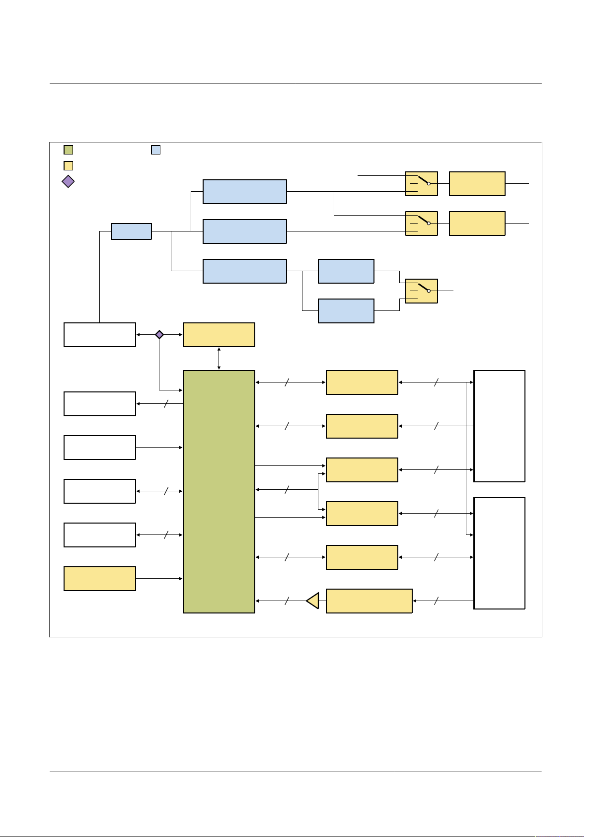
3.4 Block diagram
UM11524
First Field Verification Tool User manual
Figure 10. Block diagram
UM11524 All information provided in this document is subject to legal disclaimers. © NXP B.V. 2021. All rights reserved.
User manual Rev. 1 — 24 February 2021
9 / 34
Page 10
NXP Semiconductors
4 Setting up the FFV Tool kit
4.1 Software installation
4.1.1 Download software
Go to http://www.nxp.com/SEN-SPI-BOX to download the software.
4.1.2 System requirements
The computer system hosting the Sensor FFV Tool software and SEN-SPI-BOX
hardware must meet the following requirements:
• Windows 10 (x86, x64). Although Windows Vista, 7 are anticipated to work as well,
these systems have not been tested and are not supported.
• For each SEN-SPI-BOX, a USB (V3.0) port must be available on the host PC. NXP
anticipates the SEN-SPI-BOX will work with USB V1.1 or V2.0 ports. However, NXP
has not tested the SEN-SPI-BOX with USB V1.1 or V2.0 ports.
• The screen size shall be at least 1024 x 768 pixels. NXP does not recommend using
screens with resolution smaller than 1024 x 768 pixels. Although the software runs on
screens with lower resolution, the GUI and forms are less convenient to use.
• Software to display Adobe PDF documents is required to read the documentation and
the data sheets.
UM11524
First Field Verification Tool User manual
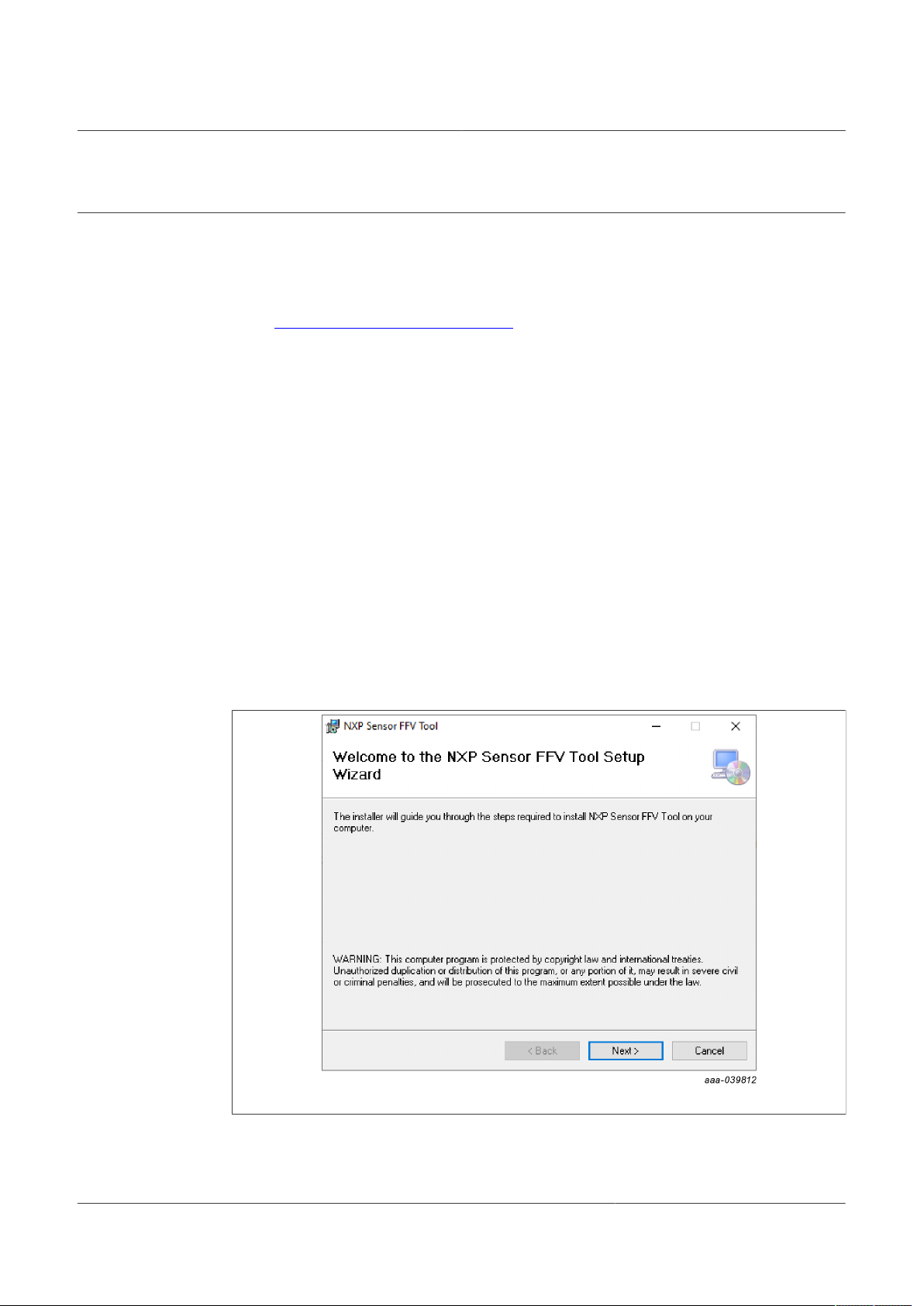
4.1.3 Setup
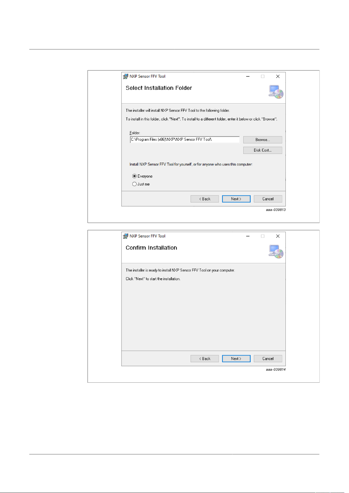
Double-click the downloaded .msi file and follow the instructions.
Figure 11. NXP Sensor FFV tool setup
NXP recommends using the default installation folder, however the installation location
can be customized.
UM11524 All information provided in this document is subject to legal disclaimers. © NXP B.V. 2021. All rights reserved.
User manual Rev. 1 — 24 February 2021
10 / 34
Page 11
NXP Semiconductors
UM11524
First Field Verification Tool User manual
Figure 12. NXP Sensor FFV installation folder
Figure 13. NXP Sensor FFV tool installation confirmation
4.2 Prepare the kit
4.2.1 Connect the kit
Connect the FFV kit via the USB Type-B cable included in the kit.
UM11524 All information provided in this document is subject to legal disclaimers. © NXP B.V. 2021. All rights reserved.
User manual Rev. 1 — 24 February 2021
11 / 34
Page 12

NXP Semiconductors
Figure 14. Connecting the kit via USB Type-B cable
A new USB design should appear in the Windows device manager as shown in
Figure 15. There is no need to install a specific driver because the FFV kit uses standard
Window COM port drivers (usbser.sys, hhdserial64.sys) already present in Windowsbased computers.
UM11524
First Field Verification Tool User manual
Figure 15. Compatible COM Port drivers
4.2.2 Launch the software
4.2.2.1 Start
Start the GUI through the launcher or double-click a .ffvpkg file (if .ffvpkg is used, skip
Section 4.2.2.2 and jump directly to step Section 4.2.2.3)
UM11524 All information provided in this document is subject to legal disclaimers. © NXP B.V. 2021. All rights reserved.
User manual Rev. 1 — 24 February 2021
12 / 34
Page 13

NXP Semiconductors
4.2.2.2 Select a project
UM11524
First Field Verification Tool User manual
Figure 16. Select a script in the First Field Verification tool
There are several ways to open projects.
Previously Opened Project: Previously opened projects are listed in “Recent projects”.
Double-click the "recent project" to reopen the project. To learn more, refer to Section 6.
Figure 17. Open an existing project
NXP Compatible sensor without dedicated package file: The user has an NXP
compatible sensor but does not have a dedicated package file. Click the menu bar and
review the existing “Predefined sensor packages”. To learn more, refer to Section 6.
UM11524 All information provided in this document is subject to legal disclaimers. © NXP B.V. 2021. All rights reserved.
User manual Rev. 1 — 24 February 2021
13 / 34
Page 14

NXP Semiconductors
UM11524
First Field Verification Tool User manual
Figure 18. Open a compatible sensor without a dedicated package file
NXP .ffvpkg file: The user has an NXP-provided .ffvpkg file. Click the “Browse” button,
select the file and open it. Alternately, drag and drop the file in “Recent projects” adding
the file to the "recent projects" list. To learn more, refer to Section 6.
Unsupported device or missing package to communicate with the device: The
user has an unsupported device or lacks the necessary package to communicate with
the sensor. In this case, use the “Standard communication protocols”. These protocols
provide basic functions to communicate with SPI, I2C, PSI5, or DSI3 sensors. To learn
more, refer to Section 5.
Figure 19. Open an unsupported device or missing a package
Note: PSI5 and DSI3 protocols necessitate special hardware which is sold separately
from the SEN-SPI-BOX kit. (SEN-PSI5-ADAPTER and SEN-DSI3-ADAPTER).
4.2.2.3 FFV kit search
The software scans all the compatible devices. If this operation fails, ensure that
everything is properly connected and retry.
UM11524 All information provided in this document is subject to legal disclaimers. © NXP B.V. 2021. All rights reserved.
User manual Rev. 1 — 24 February 2021
14 / 34
Page 15

NXP Semiconductors
Figure 20. FFV compatible device scan
UM11524
First Field Verification Tool User manual
4.2.2.4 Enable the power supplies
After the software detects the kit, enable and select the voltage for the power supplies as
needed.
Figure 21. FFV power supply voltage selection
4.2.2.4.1 VCC
When using the FFV kit standalone (no MCU attached to the sensor nor external supply),
enable the VCC supply.
If the sensor is already powered by an external source, disable the option.
UM11524 All information provided in this document is subject to legal disclaimers. © NXP B.V. 2021. All rights reserved.
User manual Rev. 1 — 24 February 2021
15 / 34
Page 16

NXP Semiconductors
4.2.2.4.2 VCCIO
VCCIO is the logic voltage of the SPI and I²C interfaces. It must be set to a value
compatible with the sensor VCC supply.
4.2.2.4.3 VPP
VPP is the high-voltage supply which could be used in specific cases. It must be carefully
used and may damage the sensor if not used correctly.
5 Using standard communication protocols
The SEN-SPI-BOX supports natively SPI and I2C protocols.
To add PSI5 and/or DSI3 automotive protocol interfaces to the SEN-SPI-BOX, adapter
boards may be purchased separately.
5.1 Native protocols
When SPI or I2C protocol is selected from the “Standard communication protocol” block,
it opens as shown in Figure 22.
UM11524
First Field Verification Tool User manual
Figure 22. Example of custom GUI selection for SPI interface
Choose the power supplies as explained Section 4.2.2.4. Select the SEN-SPI-BOX kit
(green button bottom right).
Use the debug cable provided in the kit to connect the sensor with the SEN-SPI-BOX
board.
Click on the "Select" button once erverything is configured. The software opens the
form corresponding to the selected protocol (SPI or I2C) as detailed in Section 5.1.1 and
Section 5.1.2.
UM11524 All information provided in this document is subject to legal disclaimers. © NXP B.V. 2021. All rights reserved.
User manual Rev. 1 — 24 February 2021
16 / 34
Page 17

NXP Semiconductors
5.1.1 SPI
The SPI menu offers the necessary functions to transfer data. It supports frequencies
up to 10 MHz and the four different SPÏ modes. Transfer width supports 8 to 32 bits data
transfers. There are two selections for Chip Select that correspond to the NXP MDI and
Beagle terminals.
UM11524
First Field Verification Tool User manual
Figure 23. SPI functions for data transfer
Once the configuration set, data can be easily transferred using the “Send” button.
5.1.2 I2C
This I2C interface supports up to 64 byte data transfers.
Configure the 7-bit sensor address and the frequency of the bus (up to 1 MHz).
Figure 24. I2C Interface
5.1.2.1 I2C scanner
The SEN-SPI-BOX is able to scan for I2C sensor addresses. To see all compatible
connected sensors, click the “Scan” button.
UM11524 All information provided in this document is subject to legal disclaimers. © NXP B.V. 2021. All rights reserved.
User manual Rev. 1 — 24 February 2021
17 / 34
Page 18

NXP Semiconductors
5.1.2.2 Read
Select a register start address and the number of data to read. The result is shown as an
array of 8-bit data.
5.1.2.3 Write
Select a start register and write the value in hexadecimal. Separate multiple values using
a semicolon (;).
5.2 Optional protocols
The selection of DSI3 or PSI5 protocol in the “Standard communication protocol” block
necessitates a special adapter board (SEN-PSI5-ADAPTER or SEN-DSI3-ADAPTER) for
each protocol.
1. Check and set the compatible power supply. Always refer to and set the power
2. Connect the adapter board on the SEN-SPI-BOX using the NXP MDI terminal.
3. Click the Scan button.
4. Select the PSI5/DSI3 transceiver listed.
UM11524
First Field Verification Tool User manual
settings using the value printed on the bottom of the board.Table 3 provides a
summary for convenience.
Table 3. DSI3/PSI5 adapter power settings summary
SEN-DSI3-ADAPTER SEN-PSI5-ADAPTER
VCC, VCCIO 5 V 3.3 V
VPP 13.5 V 10.5 V
Components are on the top. Check the connector coding to avoid mistakes.
Figure 25. Transceiver selection
5.2.1 DSI3
Two DSI3 interfaces are available on the SEN-DSI3-ADAPTER board: DSI3 channel 0
and DSI3 channel 1.
UM11524 All information provided in this document is subject to legal disclaimers. © NXP B.V. 2021. All rights reserved.
User manual Rev. 1 — 24 February 2021
18 / 34
Page 19

NXP Semiconductors
To enable or disable the interface for each channel, use the “DSI3 channel enable”
checkbox.
Enabling a channel automatically sends discovery pulses. Every compatible device
present on the bus is assigned a unique physical address.
Figure 26. Enable or disable the DSI3 channel
To exit PDCM mode, the corresponding DSI3 channel must be disabled.
5.2.1.1 Command and response mode (CRM)
By default the transceiver boots in CRM mode. If a sensor is connected to the bus and
owns a physical address, users may be able to send a CRM command.
The sensor manufacturer specifies the commands and the data to send.
UM11524
First Field Verification Tool User manual
Figure 27. CRM settings
5.2.1.2 Periodic data collection mode (PDCM)
Once the sensor is configured using CRM commands, the user must set the DSI3
receiver correctly for PDCM operations.
1. Selected chip time (transceiver chip time must be identical to the chip time of the DSI3
sensor).
2. Associate source ID to timeslot. If a mismatch occurs between the frame source ID
and the slot number, the mismatch raises an error.
3. Choose whether Broad Read Command (BRC) is sent every 500 µs or manually
(when the user clicks the "Update" button.
The user can then switch the DSI3 transceiver to PDCM mode by clicking the “Enter”
button. The transceiver stays in PCDM mode while the bus is powered.
To return to CRM mode, the user must power off, then power on, the associated channel
to return to CRM mode.
UM11524 All information provided in this document is subject to legal disclaimers. © NXP B.V. 2021. All rights reserved.
User manual Rev. 1 — 24 February 2021
19 / 34
Page 20

NXP Semiconductors
Figure 28. PDCM settings
5.2.1.3 Background diagnostic mode (BDM)
UM11524
First Field Verification Tool User manual
Background diagnostic mode is not supported.
5.2.2 PSI5
Two PSI5 interfaces are available on the SEN-PSI5-ADAPTER board: PSI5 channel 0
and PSI5 channel 1.
The interfaces are enabled/disabled using the “PSI5 channel enable” checkbox.
The interface only works for “Sensor to ECU” communication (ECU to Sensor
communication is not supported yet).
Figure 29. PSI5 transceiver interface
The operation mode must be selected according to the PSI5 sensor capability.
UM11524 All information provided in this document is subject to legal disclaimers. © NXP B.V. 2021. All rights reserved.
User manual Rev. 1 — 24 February 2021
20 / 34
Page 21

NXP Semiconductors
aaa- 041027
Communication Mode:
A / P / U / DPSI5 P / CRCdd L / Hntttt /
Nº of Data Bits
Error Detection
Cycle Time in µs
Nº of Time Slots per cycle
Bit Rate
Figure 30. Denomination of PSI5 operation modes
PSI5 supports both synchronous (P) and asynchronous (A) modes. Figure 30 provides a
visual summary of the PSI5 operation modes and Table 4 provides details for each field.
Table 4. PSI5 operation mode details
Field Possible values
Cycling time 200 µs to 8360 µs (32 µs step)
Number of slots per cycle 1 to 6
UM11524
First Field Verification Tool User manual
Synchronous: PCommunication mode
Asynchronous: A
16-bit: 16Number of data bits
10-bit: 10
CRC: CError detection
Parity: P
125 kbit/s: LBit rate
189 kbit/s: H
UM11524 All information provided in this document is subject to legal disclaimers. © NXP B.V. 2021. All rights reserved.
User manual Rev. 1 — 24 February 2021
21 / 34
Page 22

NXP Semiconductors
First Field Verification Tool User manual
6 Using .ffvpkg or predefined sensor packages
6.1 Connect the sensor to the FFV kit
Plug the sensor to the Sensor FFV kit. If provided by NXP, use the NXP socket board, or
connect your own board. The pinout is described in Section 3.2.
6.2 Scan for sensor
In the software, press the “Scan” button.
UM11524
Figure 31. Sensor selection page
A list of the compatible sensors appears.
6.3 Configure the sensor
Select the sensor from the list and if available, configure the SPI/I²C settings.
Note: The new configuration is applied only when the "Select" button is activated.
6.3.1 Advanced window for advanced features
To open the advanced windows, right-click any compatible sensor.
UM11524 All information provided in this document is subject to legal disclaimers. © NXP B.V. 2021. All rights reserved.
User manual Rev. 1 — 24 February 2021
22 / 34
Page 23

NXP Semiconductors
Figure 32. Advanced features
Note: This feature should be used with special care and is not synchronized with
standard functions.
This capability means that users can overwrite the sensor register without seeing it in the
other window if it is not updated.
UM11524
First Field Verification Tool User manual
Currently, there are two advanced forms:
• Register table: Quick and easy way to read and modify the sensor memory.
• Scripting: To configure the sensor, automate actions with a command list.
6.3.1.1 Register table
Figure 33 presents the values found in the registers of the sensor.
Figure 33. Register sensor content
The data presented in the sensor table, shown in Figure 33, is not real time and a
mismatch could exist between the value in the table and the actual register value. The
value is displayed in hexadecimal format.
UM11524 All information provided in this document is subject to legal disclaimers. © NXP B.V. 2021. All rights reserved.
User manual Rev. 1 — 24 February 2021
23 / 34
Page 24

NXP Semiconductors
Use filters to reduce the number of visible registers (address, register name, bit field
name).
6.3.1.2 Custom script
In parallel, custom scripts can be executed if users want to automate some actions.
To learn how to write scripts, review Section 6.5.3.1.
UM11524
First Field Verification Tool User manual
Figure 34. FFV script editor
6.4 Open the package
Press the "select" button to open the package content.
There are two types of .ffvpkg files:
• Test File (See the magnifier icon in Figure 35.)
• Datalogger File (See the graphing icon in Figure 35.)
Depending on the file, the correct form automatically opens.
Figure 35. Types of .ffvpkg files
If using .ffvscript file, jump to Section 6.5.3.
UM11524 All information provided in this document is subject to legal disclaimers. © NXP B.V. 2021. All rights reserved.
User manual Rev. 1 — 24 February 2021
24 / 34
Page 25

NXP Semiconductors
6.5 Use the package files
6.5.1 Test file
6.5.1.1 Configure the test
If available, press the wrench icon to change the test settings. Users can skip some tests
by unchecking the test in the list.
UM11524
First Field Verification Tool User manual
Figure 36. Test of an FXLS90422AES inertial sensor
6.5.1.2 Run the test
Once everything is configured, press the “Run” button. Wait while the sequence is being
executed. To view the details of the selected test, click the folder icon.
UM11524 All information provided in this document is subject to legal disclaimers. © NXP B.V. 2021. All rights reserved.
User manual Rev. 1 — 24 February 2021
25 / 34
Page 26

NXP Semiconductors
UM11524
First Field Verification Tool User manual
Figure 37. FFV running the test
When complete, export the test results by clicking “Save”. A “.ffvreport” file and a .pdf is
generated. The results are visible later when opening the file.
Close the software.
6.5.1.3 Open a test report
Open a test report file by double-clicking a “.ffvreport” file or by launching the software
and selecting the file from the window browser.
Figure 38. FFV opening the test report
UM11524 All information provided in this document is subject to legal disclaimers. © NXP B.V. 2021. All rights reserved.
User manual Rev. 1 — 24 February 2021
26 / 34
Page 27

NXP Semiconductors
This form is read-only. Re-executing any test from here is not possible.
6.5.1.4 Create a custom test file using C# .Net
Custom test files can be developed using Visual Studio IDE with C# .Net framework.
Special documentation is available from the FFV software by clicking “Create advanced
C# script” from the launcher.
6.5.2 Datalogger file
6.5.2.1 Configure the sensor
UM11524
First Field Verification Tool User manual
Figure 39. Example of configuration interface
The left panel offers many high-level settings the user may access to configure the
sensor. Do not forget to apply the settings before starting any data steam.
This panel may display differently depending on the selected file/sensor.
6.5.2.2 Configure the streaming settings
The streaming panel is split in 3 different sub panels.
6.5.2.2.1 Stream settings
The Stream settings panel allows users to select:
• “Sampling time” between two data (make sure that the communication frequency is
high enough to support the highest rate).
• “Count”: The number of samples to be collected (any non-number value is turned into
infinite).
• “Acquisition time”: Not selectable. It just gives the result of “Count” x “Sampling Time”.
• “Unit in LSB”: Unchecked. Shows the plot with the standard units, else shows in LSB.
• “Start” / “Stop”: Launch/stop the stream.
UM11524 All information provided in this document is subject to legal disclaimers. © NXP B.V. 2021. All rights reserved.
User manual Rev. 1 — 24 February 2021
27 / 34
Page 28

NXP Semiconductors
Figure 40. FFV configuring the stream settings
6.5.2.2.2 Stream info
The stream info panel displays status information about the data collection.
UM11524
First Field Verification Tool User manual
Figure 41. FFV stream information
6.5.2.2.3 Recording settings
The Recording settings panel allows the user to record the incoming data stream.
• Output file: The path of the record
• Status: Indicates whether a recording is taking place.
• Recording time: Displays how long the recording has been running.
• Record / Stop: Launches/Stops the record.
Figure 42. FFV recording the settings
6.5.2.2.4 Run the datalog
Once everything is configured, take advantage on the fast real-time data plotting.
UM11524 All information provided in this document is subject to legal disclaimers. © NXP B.V. 2021. All rights reserved.
User manual Rev. 1 — 24 February 2021
28 / 34
Page 29

NXP Semiconductors
Figure 43. Real-time graphing example
UM11524
First Field Verification Tool User manual
6.5.3 Script file
To automatically execute a list of commands, use script files to create customized scripts.
These scripts are editable using simple text keywords.
Figure 44. FFV creating customized scripts
To load the file content, drag and drop a text file into the editor area.
6.5.3.1 Create custom scripts
The available keywords are listed below and can be used to develop automatic line by
line sequences.
UM11524 All information provided in this document is subject to legal disclaimers. © NXP B.V. 2021. All rights reserved.
User manual Rev. 1 — 24 February 2021
29 / 34
Page 30

NXP Semiconductors
6.5.3.1.1 Generic sensor commands (high-level)
• RR <address> [options]: Read register command.
• WR <address> <data> [options]: Write register command.
• DR <source ID> [options]: Sensor Data Request command (Auto-Safety sensor).
6.5.3.1.2 Generic advanced sensor commands (high-level)
• MR <addess(es)> <multiplier> <delay> [options]: Multi read register command, real
time.
– address(es): Can be [@1, @2, @3] or range as [@1 - @3] (up to 1024 bytes).
– multiplier: Repeat the address sequence.
– delay: Time in µs between each command. (up to 100 ms, check the bus speed
• MD <source Id> <multiplier> <delay> [options]: Multi data-request register command,
real time).
– source Id: Can be [1, 2, 3] or range as [1 - 3].
– multiplier: Repeat the source Id sequence.
– delay: Time in µs between each command. (up to 100 ms, check the bus speed
UM11524
First Field Verification Tool User manual
compatibility).
compatibility).
6.5.3.1.3 Generic SPI commands (low level)
• S32 <data> [options]: 32-bit SPI transfer.
• S24 <data> [options]: 24-bit SPI transfer.
• S16 <data> [options]: 16-bit SPI transfer.
• S8 <data> [options]: 8-bit SPI transfer.
6.5.3.1.4 Generic I²C commands (low level)
Not supported yet.
6.5.3.1.5 Other commands (low level)
• SETV <channel> <voltage> [options]: Power supply command (Special care is required
when using this command. Applying an incorrect voltage may damage a sensor.).
– channel: VCC, VCCIO, or VPP.
– voltage: (VCC, VCCIO) OFF, 3.3, 5 - (VPP) OFF, 10.5, 13.5.
• DELAY <time> [options]: Software delay command in milliseconds, not real time, only
accurate for long timing.
• ': Comment.
6.5.3.1.6 Using [Options]
At the end of the command line, add a "-" followed by the option flag. The available flags
are:
• -D: Output result in decimal rather than hex.
• -T: Print timestamp.
UM11524 All information provided in this document is subject to legal disclaimers. © NXP B.V. 2021. All rights reserved.
User manual Rev. 1 — 24 February 2021
30 / 34
Page 31

NXP Semiconductors
6.5.3.1.7 Examples
Table 5. Example script commands
Command Command comment
rr 0x3e 'read address 3E in hexadecimal, result output is in hexadecimal.
rr 25 -t 'read register 25 (19 in hex), result output in hexadecimal, timestamp is
rr 0x12 -d 'read address 12 in hexadecimal, result output is in decimal.
wr 0x1A 0xAA 'write 0xAA in the register 0x1A.
wr 0x41 255 'write 0xFF in the register 0x41.
dr 0 -d -t 'data request channel 0 with timestamp and decimal output.
mr [0-5] 1 0 'read addresses from 0 to 5 once at the highest bus speed.
mr [0,1,2,3,4,5] 1 0 'same as above.
mr 0 20 100 -d 'read register at address 0 20 times every 100 μs with a decimal display.
md 0 5 100 'data request for channel 0, 5 times every 100 μs.
md [0,1] 10 200 -d 'data request channel 0 and 1, 20 times every 200 ms, decimal display.
UM11524
First Field Verification Tool User manual
displayed.
UM11524 All information provided in this document is subject to legal disclaimers. © NXP B.V. 2021. All rights reserved.
User manual Rev. 1 — 24 February 2021
31 / 34
Page 32

NXP Semiconductors
7 Legal information
7.1 Definitions
Draft — A draft status on a document indicates that the content is still
under internal review and subject to formal approval, which may result
in modifications or additions. NXP Semiconductors does not give any
representations or warranties as to the accuracy or completeness of
information included in a draft version of a document and shall have no
liability for the consequences of use of such information.
7.2 Disclaimers
Limited warranty and liability — Information in this document is believed
to be accurate and reliable. However, NXP Semiconductors does not
give any representations or warranties, expressed or implied, as to the
accuracy or completeness of such information and shall have no liability
for the consequences of use of such information. NXP Semiconductors
takes no responsibility for the content in this document if provided by an
information source outside of NXP Semiconductors. In no event shall NXP
Semiconductors be liable for any indirect, incidental, punitive, special or
consequential damages (including - without limitation - lost profits, lost
savings, business interruption, costs related to the removal or replacement
of any products or rework charges) whether or not such damages are based
on tort (including negligence), warranty, breach of contract or any other
legal theory. Notwithstanding any damages that customer might incur for
any reason whatsoever, NXP Semiconductors’ aggregate and cumulative
liability towards customer for the products described herein shall be limited
in accordance with the Terms and conditions of commercial sale of NXP
Semiconductors.
Right to make changes — NXP Semiconductors reserves the right to
make changes to information published in this document, including without
limitation specifications and product descriptions, at any time and without
notice. This document supersedes and replaces all information supplied prior
to the publication hereof.
Suitability for use — NXP Semiconductors products are not designed,
authorized or warranted to be suitable for use in life support, life-critical or
safety-critical systems or equipment, nor in applications where failure or
malfunction of an NXP Semiconductors product can reasonably be expected
to result in personal injury, death or severe property or environmental
damage. NXP Semiconductors and its suppliers accept no liability for
inclusion and/or use of NXP Semiconductors products in such equipment or
applications and therefore such inclusion and/or use is at the customer’s own
risk.
Applications — Applications that are described herein for any of these
products are for illustrative purposes only. NXP Semiconductors makes
no representation or warranty that such applications will be suitable
for the specified use without further testing or modification. Customers
are responsible for the design and operation of their applications and
products using NXP Semiconductors products, and NXP Semiconductors
accepts no liability for any assistance with applications or customer product
design. It is customer’s sole responsibility to determine whether the NXP
Semiconductors product is suitable and fit for the customer’s applications
and products planned, as well as for the planned application and use of
customer’s third party customer(s). Customers should provide appropriate
design and operating safeguards to minimize the risks associated with
their applications and products. NXP Semiconductors does not accept any
liability related to any default, damage, costs or problem which is based
on any weakness or default in the customer’s applications or products, or
UM11524
First Field Verification Tool User manual
the application or use by customer’s third party customer(s). Customer is
responsible for doing all necessary testing for the customer’s applications
and products using NXP Semiconductors products in order to avoid a
default of the applications and the products or of the application or use by
customer’s third party customer(s). NXP does not accept any liability in this
respect.
Export control — This document as well as the item(s) described herein
may be subject to export control regulations. Export might require a prior
authorization from competent authorities.
Evaluation products — This product is provided on an “as is” and “with all
faults” basis for evaluation purposes only. NXP Semiconductors, its affiliates
and their suppliers expressly disclaim all warranties, whether express,
implied or statutory, including but not limited to the implied warranties of
non-infringement, merchantability and fitness for a particular purpose. The
entire risk as to the quality, or arising out of the use or performance, of this
product remains with customer. In no event shall NXP Semiconductors, its
affiliates or their suppliers be liable to customer for any special, indirect,
consequential, punitive or incidental damages (including without limitation
damages for loss of business, business interruption, loss of use, loss of
data or information, and the like) arising out the use of or inability to use
the product, whether or not based on tort (including negligence), strict
liability, breach of contract, breach of warranty or any other theory, even if
advised of the possibility of such damages. Notwithstanding any damages
that customer might incur for any reason whatsoever (including without
limitation, all damages referenced above and all direct or general damages),
the entire liability of NXP Semiconductors, its affiliates and their suppliers
and customer’s exclusive remedy for all of the foregoing shall be limited to
actual damages incurred by customer based on reasonable reliance up to
the greater of the amount actually paid by customer for the product or five
dollars (US$5.00). The foregoing limitations, exclusions and disclaimers shall
apply to the maximum extent permitted by applicable law, even if any remedy
fails of its essential purpose.
Translations — A non-English (translated) version of a document is for
reference only. The English version shall prevail in case of any discrepancy
between the translated and English versions.
Security — Customer understands that all NXP products may be subject
to unidentified or documented vulnerabilities. Customer is responsible
for the design and operation of its applications and products throughout
their lifecycles to reduce the effect of these vulnerabilities on customer’s
applications and products. Customer’s responsibility also extends to other
open and/or proprietary technologies supported by NXP products for use
in customer’s applications. NXP accepts no liability for any vulnerability.
Customer should regularly check security updates from NXP and follow up
appropriately. Customer shall select products with security features that best
meet rules, regulations, and standards of the intended application and make
the ultimate design decisions regarding its products and is solely responsible
for compliance with all legal, regulatory, and security related requirements
concerning its products, regardless of any information or support that may
be provided by NXP. NXP has a Product Security Incident Response Team
(PSIRT) (reachable at PSIRT@nxp.com) that manages the investigation,
reporting, and solution release to security vulnerabilities of NXP products.
7.3 Trademarks
Notice: All referenced brands, product names, service names and
trademarks are the property of their respective owners.
NXP — wordmark and logo are trademarks of NXP B.V.
UM11524 All information provided in this document is subject to legal disclaimers. © NXP B.V. 2021. All rights reserved.
User manual Rev. 1 — 24 February 2021
32 / 34
Page 33

NXP Semiconductors
Tables
UM11524
First Field Verification Tool User manual
Tab. 1. NXP MDI connector pinout ............................... 7
Tab. 2. Beagle connector pinout ................................... 7
Tab. 3. DSI3/PSI5 adapter power settings
summary ..........................................................18
Figures
Fig. 1. NXP Sensor SPI/I2C Master Kit - SEN-SPI-
BOX ................................................................... 3
Fig. 2. SEN-SPI-BOX kit contents ................................4
Fig. 3. Attaching the SEN-GEN6-SKT board to the
SEN-SPI-BOX ................................................... 5
Fig. 4. SEN-SPI-BOX overview .................................... 6
Fig. 5. SEN-SPI-BOX interfaces ...................................6
Fig. 6. NXP MDI and Beagle connector pinout .............6
Fig. 7. Debug cable pinouts ......................................... 7
Fig. 8. Status indicators ................................................8
Fig. 9. Front LED indicators ......................................... 8
Fig. 10. Block diagram ................................................... 9
Fig. 11. NXP Sensor FFV tool setup ............................10
Fig. 12. NXP Sensor FFV installation folder .................11
Fig. 13. NXP Sensor FFV tool installation
confirmation ..................................................... 11
Fig. 14. Connecting the kit via USB Type-B cable ........12
Fig. 15. Compatible COM Port drivers ......................... 12
Fig. 16. Select a script in the First Field Verification
tool ...................................................................13
Fig. 17. Open an existing project ................................. 13
Fig. 18. Open a compatible sensor without a
dedicated package file .................................... 14
Fig. 19. Open an unsupported device or missing a
package ........................................................... 14
Fig. 20. FFV compatible device scan ........................... 15
Tab. 4. PSI5 operation mode details ........................... 21
Tab. 5. Example script commands .............................. 31
Fig. 21. FFV power supply voltage selection ................15
Fig. 22. Example of custom GUI selection for SPI
interface ...........................................................16
Fig. 23. SPI functions for data transfer ........................ 17
Fig. 24. I2C Interface ....................................................17
Fig. 25. Transceiver selection ...................................... 18
Fig. 26. Enable or disable the DSI3 channel ................ 19
Fig. 27. CRM settings ...................................................19
Fig. 28. PDCM settings ................................................ 20
Fig. 29. PSI5 transceiver interface ............................... 20
Fig. 30. Denomination of PSI5 operation modes .......... 21
Fig. 31. Sensor selection page .....................................22
Fig. 32. Advanced features .......................................... 23
Fig. 33. Register sensor content .................................. 23
Fig. 34. FFV script editor ..............................................24
Fig. 35. Types of .ffvpkg files ........................................24
Fig. 36. Test of an FXLS90422AES inertial sensor .......25
Fig. 37. FFV running the test ....................................... 26
Fig. 38. FFV opening the test report ............................ 26
Fig. 39. Example of configuration interface .................. 27
Fig. 40. FFV configuring the stream settings ................28
Fig. 41. FFV stream information ...................................28
Fig. 42. FFV recording the settings .............................. 28
Fig. 43. Real-time graphing example ........................... 29
Fig. 44. FFV creating customized scripts ..................... 29
UM11524 All information provided in this document is subject to legal disclaimers. © NXP B.V. 2021. All rights reserved.
User manual Rev. 1 — 24 February 2021
33 / 34
Page 34

NXP Semiconductors
Contents
UM11524
First Field Verification Tool User manual
1 Introduction ......................................................... 3
2 Getting started .................................................... 4
2.1 Kit contents/packing list ..................................... 4
2.2 Finding kit resources and information on
the NXP website ................................................5
3 Hardware description ......................................... 5
3.1 Kit overview ....................................................... 5
3.2 Pinout .................................................................6
3.2.1 NXP MDI connector ...........................................7
3.2.2 Beagle connector ...............................................7
3.2.3 Beagle debug cable ...........................................7
3.3 LED indicators ................................................... 8
3.3.1 Rear view ...........................................................8
3.3.2 Front view .......................................................... 8
3.4 Block diagram ....................................................9
4 Setting up the FFV Tool kit .............................. 10
4.1 Software installation .........................................10
4.1.1 Download software .......................................... 10
4.1.2 System requirements ....................................... 10
4.1.3 Setup ................................................................10
4.2 Prepare the kit ................................................. 11
4.2.1 Connect the kit ................................................ 11
4.2.2 Launch the software ........................................ 12
4.2.2.1 Start ................................................................. 12
4.2.2.2 Select a project ................................................13
4.2.2.3 FFV kit search ................................................. 14
4.2.2.4 Enable the power supplies .............................. 15
5 Using standard communication protocols ..... 16
5.1 Native protocols ............................................... 16
5.1.1 SPI ................................................................... 17
5.1.2 I2C ................................................................... 17
5.1.2.1 I2C scanner ..................................................... 17
5.1.2.2 Read ................................................................ 18
5.1.2.3 Write .................................................................18
5.2 Optional protocols ............................................18
5.2.1 DSI3 ................................................................. 18
5.2.1.1 Command and response mode (CRM) ............19
5.2.1.2 Periodic data collection mode (PDCM) ............19
5.2.1.3 Background diagnostic mode (BDM) ............... 20
5.2.2 PSI5 ................................................................. 20
6 Using .ffvpkg or predefined sensor
packages ............................................................ 22
6.1 Connect the sensor to the FFV kit ...................22
6.2 Scan for sensor ............................................... 22
6.3 Configure the sensor ....................................... 22
6.3.1 Advanced window for advanced features ........ 22
6.3.1.1 Register table .................................................. 23
6.3.1.2 Custom script ...................................................24
6.4 Open the package ........................................... 24
6.5 Use the package files ......................................25
6.5.1 Test file ............................................................ 25
6.5.1.1 Configure the test ............................................ 25
6.5.1.2 Run the test ..................................................... 25
6.5.1.3 Open a test report ........................................... 26
6.5.1.4 Create a custom test file using C# .Net ........... 27
6.5.2 Datalogger file ................................................. 27
6.5.2.1 Configure the sensor ....................................... 27
6.5.2.2 Configure the streaming settings ..................... 27
6.5.3 Script file ..........................................................29
6.5.3.1 Create custom scripts ......................................29
7 Legal information .............................................. 32
Please be aware that important notices concerning this document and the product(s)
described herein, have been included in section 'Legal information'.
© NXP B.V. 2021. All rights reserved.
For more information, please visit: http://www.nxp.com
For sales office addresses, please send an email to: salesaddresses@nxp.com
Date of release: 24 February 2021
Document identifier: UM11524
 Loading...