

Page 1

UM11505
LPCXpresso55S06 Development Boards
Rev. 1.2 — 19 February 2021 User manual
Document information
Info Content
Keywords LPC55S06, LPC55S0x, LPCXpresso55S06, LPC55S06-EVK
Abstract LPCXpresso55S06 development board user manual
Page 2

NXP Semiconductors
UM11505
LPCXpresso55S06 Development Boards
Revision history
Rev Date Description
1.2 20210219 Corrected Typo in
1.1 20210217 Information added in
1.0 20201005 Initial internal release.
Section 10 “Errata”, Changed A2 to A1
Section 10 “Errata”
Contact information
For more information, please visit: http://www.nxp.com
For sales office addresses, please send an email to: salesaddresses@nxp.com
UM11505
User manual Rev. 1.2 — 19 February 2021 2 of 18
All information provided in this document is subject to legal disclaimers. © NXP B.V. 2021. All rights reserved.
Page 3
NXP Semiconductors
1. Introduction
The LPCXpresso™ family of boards provides a powerful and flexible development system
for NXP's LPC Cortex®-M family of MCUs. They can be used with a wide range of
development tools, including NXP's MCUXpresso IDE, Keil uVISION and IAR Embedded
Workbench. The LPCXpresso55S06 board (order code LPC55S06-EVK) is the evaluation
and development platform for the LPC55S0x/LPC550x families of MCUs.
See https://www.nxp.com/demoboard/LPC55S06-EVK for more information on these
boards, including tutorial videos, development software and board hardware design files.
The abbreviation LPC55S0x is used to collectively refer to the LPC55S0x/LPC550x family
device on the board.
UM11505
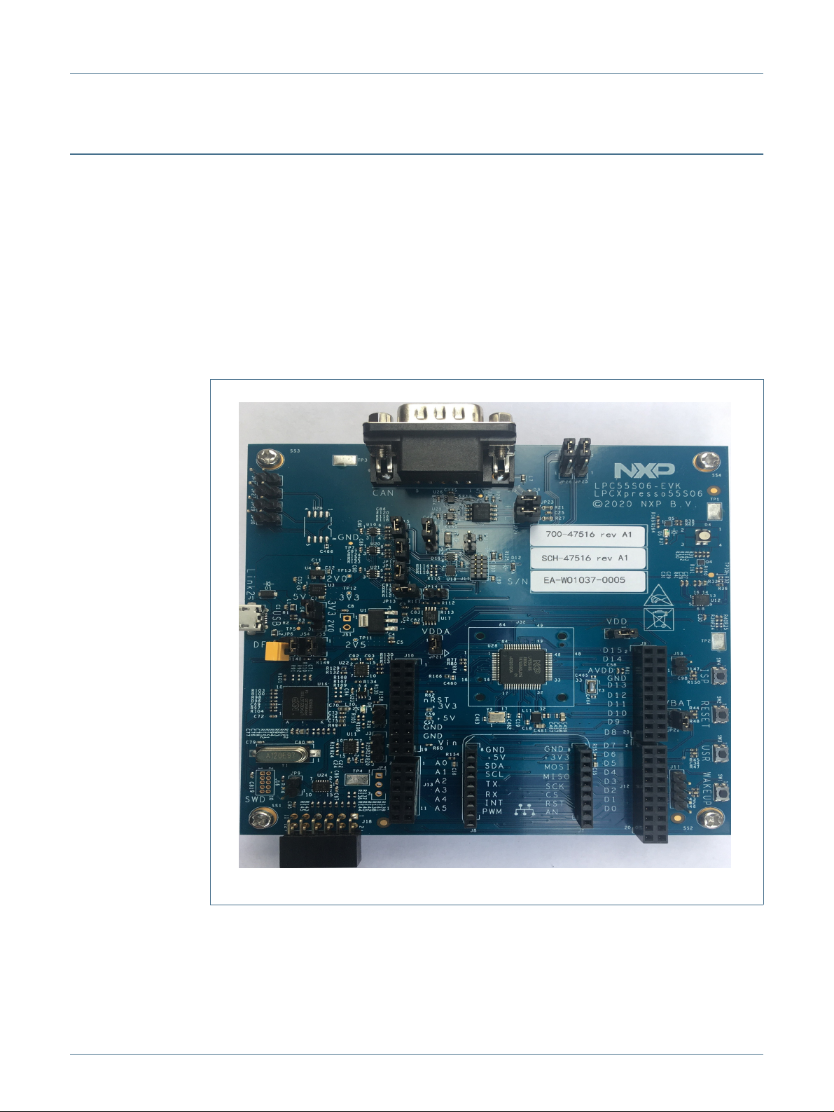
LPCXpresso55S06 Development Boards
Fig 1. LPCXpresso55S06
The LPCXpresso55S06 board includes the following features:
• LPC55S06 Cortex-M33 processor
• Onboard, high-speed USB, Link2 debug probe with CMSIS-DAP and SEGGER J-Link
protocol options
UM11505 All information provided in this document is subject to legal disclaimers. © NXP B.V. 2021. All rights reserved.
User manual Rev. 1.2 — 19 February 2021 3 of 18
Page 4
NXP Semiconductors
• UART and SPI port bridging from LPC55Sxx target to USB via the onboard debug
probe
• Optional external debug probes with trace option (10 or 20 pin Cortex-M connectors)
• External crystal oscillators
• RGB user LED
• Reset, ISP, User/Wakeup and user buttons
• Multiple Expansion options, including Arduino UNO, Mikroe Click and PMod
• CAN-FD controller and onboard CAN transceiver
• NXP FXOS8700 accelerometer
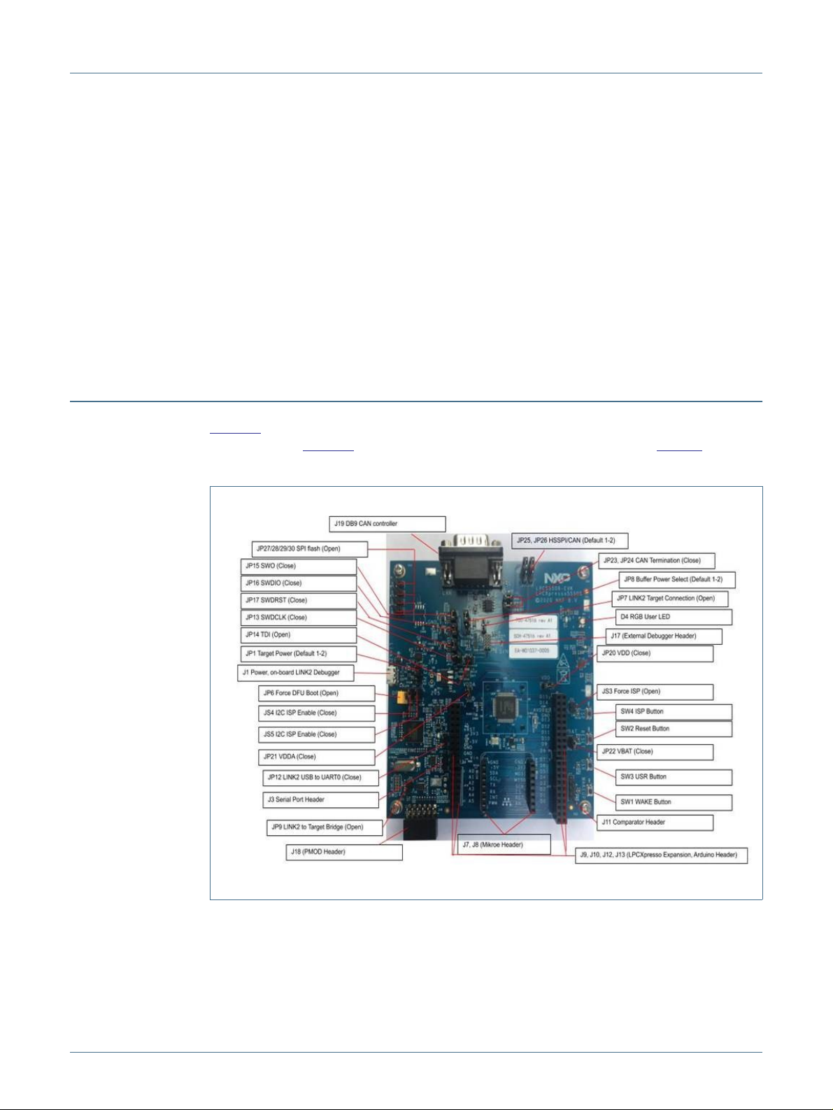
2. Board layout and Settings
Figure 2 shows the layout of the board (top side), indicating the default location of the
jumpers, while Figure 3 shows locations of the connectors and headers. Table 1 provides
a description of connectors, jumpers, LEDs and buttons.
UM11505
LPCXpresso55S06 Development Boards
Fig 2. Default jumper positions
UM11505 All information provided in this document is subject to legal disclaimers. © NXP B.V. 2021. All rights reserved.
User manual Rev. 1.2 — 19 February 2021 4 of 18
Page 5
NXP Semiconductors
UM11505
LPCXpresso55S06 Development Boards
Table 1. Indicators, buttons, connectors and LEDs
Circuit
reference
D5 Target power indicator LED n/a n/a
D8 Link2 boot LED n/a
D4 RGB User LED (Tri-color Red/Green/Blue) n/a Section 7.4
JP8 Buffer Power Selection
JP6 Link2 (LPC43xx) force DFU boot.
JP7 Target processor selection for the on-board Debug Probe.
JP12 LINK2 USB to UART0.
JP9 When open (default), the "Bridge" UART and SPI connections from the
JP1 Target VDD power selection. An external supply voltage to the
Description Default Reference
For On-board Target place in position 1-2 (default)
For Off-board Target place in position 2-3
Leave this jumper open (default) for Link2 to follow the normal boot
sequence. The Link2 will boot from internal flash if image is found there.
With the internal flash erased the Link2 normal boot sequence will fall
through to DFU boot.
Install this jumper to force the Link2 to DFU boot mode. Use this setting
to reprogram the Link2 internal flash with a new image (using the
LPCScrypt utility) or to use the MCUXpresso IDE with CMSIS-DAP
protocol.
Note that the Link2 flash is pre-programmed with a version of
CMSIS-DAP firmware by default.
Jumper open (default) the LPC55Sxx Target SWD interface enabled.
Normal operating mode where the Target SWD is connected to either
the on-board Link2 Debug Probe or an external Debug Probe.
Jumper shunted, the LPC55Sxx Target SWD interface is disabled. Use
this setting only when the on-board Link2 Debug Probe is used to debug
an off-board target MCU.
Installed if LINK2 USB to UART0 is used, and then, JP9 must be open.
(default)
Open if J3 external UART connection such as FTDI-USB is used, and
then, JP9 must be to closed.
Link2 probe are driven to the LPC55Sxx target UART0 and HSSPI.
Jumper shunted when using the HSSPI interface including connector
J7, J9, and J18, and/or FC0 UART at JP3. Note that this disables the
Link2 SPI and UART (bridge) connections.
LPC55Sxx can also be applied through pin 2 of this header.
Section 4.1
1-2
Open
Open Section 4.
Section 3.1,
Section 4.4
Section 3.,
Section 4.
Installed Section 6.1
Open Section 4.
1-2 (3.3V)
2-3 (2.0V)
Section 5.
J1 Link2 Debug Probe connector
Micro USB type B connection for the on-board Link2 Debug Probe.
Note: do not use this connection when using an external Debug Probe.
J17 10 pin external debug probe / off board target connector
This standard Cortex-M debug connector is used either to (1) connect
and off-board debug probe or (2) to connect an external debug target.
UM11505 All information provided in this document is subject to legal disclaimers. © NXP B.V. 2021. All rights reserved.
User manual Rev. 1.2 — 19 February 2021 5 of 18
n/a Section 5.
n/a Section 3.1.3
Page 6
NXP Semiconductors
UM11505
LPCXpresso55S06 Development Boards
Table 1. Indicators, buttons, connectors and LEDs
Circuit
reference
J3 Serial port header
J13 Analog In/Out Comparator header. n/a Section 4.
JP20 Power to MCU VDD, once removed, it can be used to measure VDD
JP21 Power to MCU VDDA, once removed, it can be used to measure VDDA
JP22 Power to MCU VBAT, once removed, it can be used to measure VBAT
JP13 SWDCLK, keep it installed if LINK2 Debugger (J1) is used. Open if
JP14 TDI, keep it open, used for JTAG boundary scan if applicable, it doesn't
JP15 SWO, keep it installed if LINK2 Debugger (J1) is used. Open if external
JP16 SWDIO, keep it installed if LINK2 Debugger (J1) is used. Open if
JP17 SWDRST, keep it installed if LINK2 Debugger (J1) is used. Open if
JP27,JP28,J29
,JP30
JS3 Forced ISP mode. To force the MCU into ISP mode, close the jumper,
JS4. JS5 Jumpers for the I2C bridge between LINK2 and target, must be installed
J9,J10,J12,J13 LPCXpresso expansion connectors, including Arduino R3 compatible
J18 PMod expansion connector / Host interface connector
J19 CAN-FD controller
Description Default Reference
n/a Section 6.
0.1" header providing convenient access to Flexcom 0 USART (the
USART used for ISP boot). When using this port, ensure jumper JP9 is
installed to disable the Link2 connection to this port and JP12 is open.
Installed Measuring
current.
Installed Measuring
current.
Installed Measuring
current.
Installed
external debugger is used and connected on J17.
Open Section 3.1.3
apply to any SWD debuggers.
debugger is used and connected on J17.
external debugger is used and connected on J17.
external debugger is used and connected on J17.
Jumpers on SPI recovery mode. Open
and reset the board. Don't forget to keep it open if you don't want MCU
in the ISP mode.
if I2C ISP is needed.
site. Provides connectivity to SPI (high-speed SPI), USART (Flexcom
1), I2C (Flexcom 3 and Flexcom 1), I2S (Flexcom 7), ADC0, GPIO and
PLU pins.
This connector provides access to the HSSPI and I2C (Flexcom 1) ports
that support LPC55Sxx ISP mode, along with 2 GPIO lines. When using
the HSSPI port at this connector ensure jumper JP9 is installed to
disable the connection to the Link2 debug probe and JP12 is open.
DB9 Male connector to CAN-FD network.
Installed Section 3.1.3
Installed Section 3.1.3
Installed Section 3.1.3
Open
Open
n/a
n/a Expansion
n/a
LPC55Sxx
device supply
current
LPC55Sxx
device supply
current
LPC55Sxx
device supply
current
Section 3.1.3
Section 8.
connectors
Section 7.1
UM11505 All information provided in this document is subject to legal disclaimers. © NXP B.V. 2021. All rights reserved.
User manual Rev. 1.2 — 19 February 2021 6 of 18
Page 7

NXP Semiconductors
Table 1. Indicators, buttons, connectors and LEDs
Circuit
reference
J7,J8 Mikroe Click site
SW4 ISP/User button
SW1 Wake/User button
SW3 User button
SW2 Reset button
Description Default Reference
Provides connectivity to standard Mikroe Click connectors. Shares SPI,
ADC, I2C and USART connections with the J9, J10, J12, J13 expansion
connectors.
When pressed, this button connect sport pin P0_5 to ground. Hold this
button down while pressing and releasing Reset (SW2) to force the
LPC55Sxx into ISP mode. Port P0_5 may also be reconfigured as a
GPIO in user application code to enable this button to be used for other,
user-defined purposes.
This button, when pressed, pulls P0_28 to ground. A 330K ohm pull up
to VDD is connected to P0_28.
This button, when pressed, pulls P1_9 to ground. A 100K ohm pull up to
VDD is connected to P1_9.
When pressed, reset is applied to the LPC55Sxx, expansion connector
(Arduino reset) J10, the Mikroe Click site reset, and U18 (debug
connector J17 reset when debugging an off-board target).
3. Getting started
UM11505
LPCXpresso55S06 Development Boards
n/a
n/a
n/a Section 7.5.2
n/a Section 7.5.2
n/a
Section 8.
Section 7.5.1
Section 7.5.3
This section describes how to first power up the board and then how to start a first debug
session using the MCUXpresso SDK. The board is pre-programmed with a simple
program indicating that the target MCU is running. Connect a micro USB cable from
connector J1 to a host computer or power supply to power-up the board and run this
program.
The following debug probes can be used with those development and the board (check
compatibility between debug probe and IDE used, including support for Arm Cortex M33
cores):
• On-board debug probe (LPC4322 “Link2”) from connector J1
• LPC-Link2 (OM13054) debug probe from NXP or Embedded Artists
• P&E Micro probes
• Keil ULINK2 probes
• IAR I-Jet probes
Other debug probes may also be supported by IAR and Keil tools and by other
IDEs/debug tools; refer the websites of these companies for further information.
3.1 Starting a debug session using the on-board (Link2) Debug Probe
By default, the Board is configured to use the on-board Debug Probe (Link2) to debug the
on-board target (LPC55Sxx), using the CMSIS-DAP debug protocol pre-programmed into
the Link2 Flash memory. The MCUXpresso IDE or other development tools that support
UM11505 All information provided in this document is subject to legal disclaimers. © NXP B.V. 2021. All rights reserved.
User manual Rev. 1.2 — 19 February 2021 7 of 18
Page 8

NXP Semiconductors
the CMSIS-DAP protocol can be used in the default configuration. Check with your
toolchain vendor for availability of specific device support packs for the LPC55Sxx series
devices.
Note that when using the MCUXpresso IDE, the on-board Link2 can also be booted in
DFU mode by installing a jumper on JP6; if this is done then the IDE will download
CMSIS-DAP to the probe as needed. Using DFU boot mode will ensure that the most
up-to-date / compatible firmware image is used with the MCUXpresso IDE.
NOTE: if the Debug Probe is set up to boot in DFU mode, the USB bridge functions
(virtual COM port) and Debug Probe features will not be available if the board is not first
initialized by the MCUXpresso IDE.
3.1.1 Installation steps for use with MCUXpresso IDE
Download and install the MCUXpresso IDE.
Configure and download an SDK package (with the MCUXpresso IDE tool chain option
selected) from the MCUXpresso SDK Builder utility (http://mcuxpresso.nxp.com).
Ensure jumper JP8 is fitted in position 1 - 2 (local target powered), and JP7 is not installed
(target SWD enabled). These are the default positions set during board manufacture.
UM11505
LPCXpresso55S06 Development Boards
Connect the board to the USB port of your host computer, connecting a micro USB cable
to connector J1. The board will boot and run the pre-installed demo.
The board is now ready to be used with the MCUXpresso SDK examples for the
LPCXpresso55S06.
When the board is used for the first time, it is recommended to force the LPC55Sxx target
into a known state by performing an ISP boot before attempting to run your first example
code. This can be achieved by pressing and holding down the ISP button while pressing
and releasing the reset button or installing the LPC55Sxx ISP jumper(JS3) and then reset
the board.
3.1.2 Installation steps to use Keil and IAR tools with on-board debug probe
Download and install LPCScrypt (https://www.nxp.com/lpcscrypt). This will install required
drivers for the board. Note that the Link2 (LPC4322 device) is pre-programmed with
CMSIS-DAP firmware. If you have previously installed LPCScrypt please ensure version
2.1 or later is installed.
Ensure jumper JP8 is fitted in position 1-2 (local target powered), and J7 is not installed
(target SWD enabled). These are the default positions set during board manufacture.
The Link2 Debug Probe on the board will have been programmed with CMSIS-DSP
firmware during manufacture, but can also be updated with J-link OB for LPC-Link2. To
start the board with this firmware running, ensure JP6 is not installed as power is
connected, so the Link2 Debug Probe boots from internal flash. If you wish to
update/change the Link2 firmware please follow the steps described in Section 4.2.
Connect the Board to the USB port of your host computer, connecting a micro USB cable
to connector J1 ("Debug-Link"). The board will boot and run the pre-installed demo. Allow
about 30 seconds for the Link2 devices to enumerate for the first time. It is not necessary
to check the Hardware Manager on your host computer, however if this is done there will
UM11505 All information provided in this document is subject to legal disclaimers. © NXP B.V. 2021. All rights reserved.
User manual Rev. 1.2 — 19 February 2021 8 of 18
Page 9

NXP Semiconductors
be five devices (if using CMSIS-DAP protocol); four under Human Interface Devices
(CMSIS-DAP, LPC-SIO, two HID Compliant Devices, and a USB Input Device) and one
under Ports (LPC-LinkII Ucom.)
Your board is now ready to use with your 3rd party tool. Follow the instructions for those
tools for using a CMSIS-DAP probe. MCUXpresso IDE can also be used with the board
after setting up the board this way.
When the board is used for the first time, it is recommended to force the target into known
state by performing an ISP boot before attempting to run your first example code. This can
be achieved by pressing and holding down the ISP button while pressing and releasing
the reset button.
3.1.3 Starting a debug session using an external Debug Probe
Code running on the LPC55Sxx target can be debugged using an external Debug Probe
that conforms to the standard ARM Cortex-M debug connector. To use an external Debug
Probe connect the probe to the SWD connector (J17), uninstall JTAG/SWD related
jumpers, JP13, JP14, JP15, JP16, and JP17, so that the Link2 Debug Probe signals do
not contend with the SWD interface signals from the external Debug Probe, and connect
power via the micro USB connector J1.
UM11505
LPCXpresso55S06 Development Boards
Also note that the VCOM function provided by the on-board Debug Probe is not available
when using an external debug probe. Then, J3 serial port header can be served as an
alternative to provide convenient access to Flexcomm 0 USART. When using this port,
ensure jumper JP9 is installed and JP12 is open.
UM11505 All information provided in this document is subject to legal disclaimers. © NXP B.V. 2021. All rights reserved.
User manual Rev. 1.2 — 19 February 2021 9 of 18
Page 10

NXP Semiconductors
4. On-board (Link2) Debug probe
This section describes the features provided by the on-board Link2 Debug Probe,
including how to use this to debug an exernal target.
The Link2 Debug Probe is implemented using an LPC432x MCU (circuit reference U16),
which provides a high speed USB port interface to the host computer that runs the
development tools. This device is not intended for developer use, and should only be used
with approved firmware images from NXP. The Link2 on-chip flash memory is factory
programmed with a firmware image that supports CMSIS-DAP debug protocol, but also
includes other USB end point functions:
• Virtual COM (VCOM) port: a serial device that can be used with any host computer
application design for serial port communication (e.g. Teraterm, puTTY, etc.) Set the
terminal program for baud rate to 115200, no parity, 8 bit data, 1 stop bit, no flow
control.
• SWO trace end point: this virtual device is used by MCUXpresso to retrieve SWO
trace data. See the MCUXpresso IDE documentation for more information.
• I2C/SPI bridges: bridge device from I2C and SPI ports of the LPC target.
UM11505
LPCXpresso55S06 Development Boards
All of these devices are independent of each other and of the CMSIS-DAP debug device
that is enumerated when the board is connected to a host computer; for example, the
VCOM port can be used if the board is running an application when no debugger is
running.
In order to correctly install and use the Link2 device on the LPCXpresso55S06 (required
for any debugging purpose) for Windows host computers, install the drivers first. These
drivers will automatically be installed when MCUXpresso IDE has already been installed.
If these IDEs are not being used, it is recommended LPCScrypt be installed as this also
includes the required drivers. All these tools and utilities are available for free download at
https://www.nxp.com/lpcscrypt.
The CMSIS-DAP firmware image installed at the factory (and by LPCScrypt) will uniquely
identify itself to the host computer so that more than one board can be connected to that
host computer at any time. Some toolchains cannot discern between multiple debug
devices; refer to your toolchain documentation for more information (note the
MCUXpresso IDE does support multiple LPCXpresso board targets.)
Note: The Link2 only boots when the board is power cycled; the reset button on the board
does not reset the Link2.
When using MCUXpresso IDE, the Link2 can be automatically booted with the latest /
most appropriate firmware for that IDE version by installing JP6 (DFU jumper) before
powering up the board. This is the recommended approach for the MCUXpresso IDE.
Note that if JP6 is installed when powering the board then the VCOM port (and other
devices mentioned above) device will not appear until the MCUXpresso IDE boots the
Debug Probe. The Debug Probe is booted once a debug session is started (that is, the
IDE attempts to download code to the target).
UM11505 All information provided in this document is subject to legal disclaimers. © NXP B.V. 2021. All rights reserved.
User manual Rev. 1.2 — 19 February 2021 10 of 18
Page 11

NXP Semiconductors
4.1 Link2 boot LED
LED D8 is the Link2 MCU BOOT0_LED indicator. This LED reflects the state of Link2
MCU pin P1_1. When the boot process fails, D8 will toggle at a 1 Hz rate for 60 seconds.
After 60 seconds, the Link2 MCU is reset.
4.2 Programming the Link2 firmware
As mentioned earlier in this section, it is not normally necessary to program the Link2
firmware. However, this can easily be accomplished using the supporting utility,
LPCScrypt.
To program the Link2 Flash the Link2 device (LPC432x) must be in DFU mode. If the
Link2 already has a valid image in the flash, it will need to be forced into DFU mode by
placing a jumper shunt on JP6 (DFU), and power cycling (disconnecting then
reconnecting power via J1.) Link2 MCU programming is performed using the LPCScrypt
utility (see http://www.nxp.com/lpcscrypt). Instructions for using the tool are located at the
same web page
After installing LPCScrypt, use either the “Program LPC-Link2 with CMSIS-DAP” or
“Program LPC-Link2 with JLink” utilities provided in that installation to update the
firmware, following on-screen instructions.
UM11505
LPCXpresso55S06 Development Boards
4.3 VCOM port
The identifier of the VCOM port will vary between boards and hosts as each board will
enumerate with a unique identifier. On Windows, to determine the COM port, open the
Windows operating system Device Manager. This can be achieved by going to the
Windows operating system Start menu and typing "Device Manager" in the search bar. In
the device manager look under "Ports"; the LPC-LinkII UCom Port device and its name
should be visible. NOTE: this VCOM port will only appear if (a) the Debug Probe has been
programmed with the CMSIS-DAP firmware and the Debug Probe DFU link (JP6) is
removed at power up, or (b) if the Debug Probe has been configured for DFU boot (JP6
installed) at power up and MCUXpresso IDE has booted it (by starting a debug session.
If the J-Link firmware image has been programmed into the Debug Probe and DFU boot
mode is not being used, then a VCOM device called J-Link CDC UART port will appear
instead of the LPC-LinkII UCom port.
4.4 Configuring the LPCXpresso55S16 to debug an off-board target
The LPCXpresso55S06 board's Link2 Debug Probe may be used to debug an off-board
target MCU. The on-board Link2 Debug Probe is capable of debugging target MCU's with
a VDDIO range of 1.6V to 3.6V. To keep the on-board target LPC55Sxx MCU from
interfering with the SWD interface, JP7 must be closed. The Link2 Debug Probe SWD
should be connected by a ribbon cable between the J17 connector to the off-board target
MCU SWD interface. Power the LPCXpresso55S06 board from the Link USB connector
J1, and fit jumper JP8 across pins 2 - 3 (External Target).
5. Board Power
The LPCXpresso55S06 board requires +5V input to power the on-board voltage low
dropout linear regulators, of which there are 3, circuit reference U1, U3 and U4. .
UM11505 All information provided in this document is subject to legal disclaimers. © NXP B.V. 2021. All rights reserved.
User manual Rev. 1.2 — 19 February 2021 11 of 18
Page 12

NXP Semiconductors
The Link2 Debug probe has a 2.5V regulator (U1) which draws power from USB
connector J1 ("Debug Link") only.
There are two other regulators, providing the option of 2.0V (U4) or 3.3V (U3) to the other
devices on the board; these regulators can be powered by the USB Debug Link connector
(J1).
The +5V sources above are connected via protection diodes to prevent reverse powering
of any of them by another source. The +5V output of these combined sources is also
connected to the Arduino and Mikroe expansion sites.
Note that the FXOS8700 Accelerometer requires the board to be configured for 3.3V
operation.
CAN-FD transceiver, circuit reference U9, TJA1044, is populated to support CAN-FD
communication. CAN-FD transceiver requires +5V supply.
For further details, refer to the board schematics.
5.1 Measuring LPC55Sxx device supply current
UM11505
LPCXpresso55S06 Development Boards
Current supply to the LPC55Sxx Core can be measured via JP20 for VDD, JP21 for
VDDA, and JP22 for VBAT.
5.2 2.0V operation
Please note the minimum voltage supply for the LPC55S0x/ devices is 1.8 V, but, the
variations in the 1.8V regulator tolerance and/or loading on the regulator may cause the
brown-out detect (BOD) to trigger, as the result, we have changed low dropout linear
regulator from 1.8V on LPC55S16 EVK board to 2.0V on LPC55S06 EVK board.
6. Board serial connections
This section describes connections between LPC55Sxx on-board serial peripherals and
connectors for use with off-board devices.
6.1 USART header
Header JP3 is provided as a convenient way to use an LPC55Sxx USART with a serial to
USB cable. Flexcom 0 ports (P0_29 and P0_30) are used for this feature, since these
ports are assigned for USART ISP mode. Note that these ports are shared with the Link2
debug probe (LPC4322) and PMod connector; when using this header ensure that there
is no conflicting device connected to the PMod connector and that jumper JP9 is installed
to disable the connection to the Link2 and JP12 jumper should be open.
7. On-board peripherals
This section describes how the on-board peripheral devices of the Board are connected to
the LPC55Sxx and relevant configuration options. For full details of these devices please
refer to the individual device datasheets. For circuit further details, refer to the board
schematics.
UM11505 All information provided in this document is subject to legal disclaimers. © NXP B.V. 2021. All rights reserved.
User manual Rev. 1.2 — 19 February 2021 12 of 18
Page 13

NXP Semiconductors
7.1 CAN-FD Connector
The LPC55S0x MCU includes a CAN-FD controller. On LPCXpresso55S06 board, P1.2
(IOCON Function 1) and P1.3 (IOCON Function 1) are configured as CAN_TXD and
CAN_RXD respectively. A CAN-FD transceiver, U9, TJA1044, is populated on the board
with level shifters between LPC55S06 target and CAN-FD transceiver to support both
2.0V and 3.3V. LPCXpresso55S06 board incorporates a DB9 connector (J19) to support
CAN-FD communication.
CAN_TXD and CAN_RXD pins are shared with HSSPI_CLK and HSSPI_MISO pins.
JP25 and JP26 are used to select the peripherals. Default positions are for CAN-FD
controller.
CAN-FD software driver and CAN Open examples are provided as part of the
LPCXpresso55S06 SDK.
7.2 Accelerometer
The board includes an NXP FXOS8700 accelerometer, interfaced to Flexcom 0 (ports
P0_24 and P0_25) with its interrupt output connected to P1_23. The accelerometer has
an I2C address of 0b0001111X.
UM11505
LPCXpresso55S06 Development Boards
I2C software drivers are provided as part of the LPCXpresso55S06 SDK, and the
example code is provided to illustrate how to read values from the accelerometer.
7.3 Crystals
For applications requiring accurate clock, two external crystal oscillators are provided on
the board,16MHz crystal on XTAL32M pins and 32.768KHz on XTAL32K pins.
External capacitors are not required on the crystal pins as LPC55S06 has embedded
capacitor banks for both XTAL32M and XTAL32K. See the "LPC55S0x/LPC550x Cap
Bank API" chapter of the LPC55S0x/LPC550x User Manual for further information.
7.4 RGB User LED
An User controlled RGB LED is provided on the Board. The LEDs in this device are
controlled by LPC55Sxx ports P0_21 (Red), P0_22 (Blue), P0_18 (Green) with the LEDs
being illuminated when the respective GPIO pin is set to high.
7.5 Buttons
Four buttons are provided on the LPCXpresso55S06 board, as described in this section.
7.5.1 ISP (SW4)
P0_5 is pulled up to VDD via a 100kohm resistor; pressing this button will pull P0_5 low.
This port is read by the LPC55Sxx boot code to determine if the MCU should enter In
System Programming (ISP) mode. The main purpose of this button is to force the
LPC55Sxx into ISP mode at boot time; to do this hold down this button while pressing and
releasing the Reset button, or while connecting power to the board. While the main
purpose of ISP mode is to program the flash of the LPC55Sxx, forcing the MCU into this
mode places it into a known state in which development tools can gain debug control. If an
UM11505 All information provided in this document is subject to legal disclaimers. © NXP B.V. 2021. All rights reserved.
User manual Rev. 1.2 — 19 February 2021 13 of 18
Page 14

NXP Semiconductors
application in flash is crashing or disabling the SWD port unintentionally, then ISP mode
can be useful to recover control of the board. Refer to the LPC55S0x User Manual for
more information on ISP mode.
The ISP button can also be used in user application code. Care should be taken if P0_5 is
configured as an output driving high, since pressing this button will short it to ground.
Note that jumper JS3 may also be used as a convenient way to always assert ISP when
the LPC55Sxx is reset or powered up.
7.5.2 User (SW3) and Wakeup (SW1) buttons
The User (SW3) and Wakeup (SW1) buttons are intended for user application use. These
buttons pull ports P1_9 (User) with 100kohm pull-up resistor and P0_28 (Wakeup) with
330kohm pull-up resistor low when the button is pressed.
7.5.3 Reset (SW2)
Pressing this button will assert reset to the LPC55Sxx and to the Mikroe and Arduino
connector sites. Note that the Link2 Debug Probe (LPC4322) is not reset when this button
is pressed.
UM11505
LPCXpresso55S06 Development Boards
8. Expansion connectors
The LPCXpresso55S0x includes 3 expansion connector sets, incorporating support for
Arduino UNO R3, Mikroe Click and PMod standards. The Arduino UNO connector
footprint is surrounded by additional connectors that are compatible with other
LPCXpresso V3 boards. For further details, refer to the board schematics.
8.1 Mikroe Click Site
The connectors J7 and J8 provide a Mikroe Click module site for the wide range of
add-on modules available from MikroElektronika. Note that this site shares the same SPI,
I2C and UART connections as the Arduino/LPCXpresso V3 expansion connectors.
8.2 Host / PMod Connector
Connector J18 is a connector which provide convenient access for a remote host to the
SPI and I2C ports of the LPC55Sxx that support ISP mode. When setting up the Board to
be used with a host, jumper JP9 must be installed to prevent conflict with the Link2 (which
can also emulate an SPI or I2C host).
8.3 Arduino and LPCXpresso V3 expansion connectors
The connectors J9, J10, J12, J13, provide Arduino UNO R3 compatibility and access to
several other signals for use in prototyping. The overall footprint is compatible with the
LPCXpresso V3 expansion connector footprint used on other LPCXpresso boards of this
type. Note that some ports used on these connectors are shared with other
devices/connectors on the board, including the Mikroe Click site, CAN-FD, and RGB LED.
Refer to the schematic for further information.
When using an Arduino shield with the Board, align the Arduino shield (SCL) with pin 1 of
connector J9 on the LPCXpresso55S06 board.
UM11505 All information provided in this document is subject to legal disclaimers. © NXP B.V. 2021. All rights reserved.
User manual Rev. 1.2 — 19 February 2021 14 of 18
Page 15

NXP Semiconductors
Table 2. Arduino and LPCXpresso V3 expansion connections
Expansion connector Port
J9 The odd number pins are compatible with Arduino Uno rev3 Digital
15:8, AREF, SDA & SCL connector. The even numbered pins are
used for external access and expansion of LPC55Sxx signals not
used by the Arduino Uno rev3 compatible interface.
J12 The odd numbered pins 1 – 15 are compatible with Arduino Uno rev3
Digital 7:0 connector. The even numbered pins, and odd numbered
pins 17 and 19, are used for external access and expansion of
LPC55Sxx signals not used by the Arduino Uno rev3 compatible
interface.
J10 The even numbered pins 6 – 20 are compatible with the Arduino Uno
rev3 Power connector standard.
P13 The even numbered pins 2 – 12 are compatible with Arduino Uno
rev3 Analog connector. The odd numbered pins are used for external
access and expansion of LPC55Sxx signals not used by the Arduino
Uno rev3 compatible interface.
9. Miscellaneous Board Features
UM11505
LPCXpresso55S06 Development Boards
10. Errata
This section describes miscellaneous board features that we not covered elsewhere in
this manual.
9.1 LPC55Sxx ADC references and inputs
The LPC55Sxx ADC positive reference is connected to VREFP and the negative
reference to ground internally. VREFP is either 3.3V or 2.0V depending on the position of
JP1.
An external differential ADC input signal can be applied at J13 or at the JP4 expansion
connector. This connection is routed to PIO0_16 and PIO0_23.
There is an issue with the layout where over power consumption (5-30 mA over expected
current) can occur due to poor grounding using vias.
One particular area as shown below is the splitted ground between VSS_DCDC pin 30
and input/output capacitors.
To prevent the over power consumption, please solder a thick wire between Pin 30 and
the nearby GND as shown below (red wire).
This will be fixed in the next board revision (A1).
UM11505 All information provided in this document is subject to legal disclaimers. © NXP B.V. 2021. All rights reserved.
User manual Rev. 1.2 — 19 February 2021 15 of 18
Page 16

NXP Semiconductors
UM11505
LPCXpresso55S06 Development Boards
Fig 3. Prevention from over power consumption
11. Board operating conditions
These boards have been designed for use in laboratory conditions (0 to 50 degrees
Celsius) and should not be used for extended temperature testing. Refer to the data sheet
of the LPC55xx MCU being used for full operating conditions for that device.
UM11505 All information provided in this document is subject to legal disclaimers. © NXP B.V. 2021. All rights reserved.
User manual Rev. 1.2 — 19 February 2021 16 of 18
Page 17

NXP Semiconductors
13. Contents
1 Introduction . . . . . . . . . . . . . . . . . . . . . . . . . . . . 3
2 Board layout and Settings . . . . . . . . . . . . . . . . 4
3 Getting started . . . . . . . . . . . . . . . . . . . . . . . . . . 7
3.1 Starting a debug session using the on-board
(Link2) Debug Probe. . . . . . . . . . . . . . . . . . . . . 7
3.1.1 Installation steps for use with MCUXpresso IDE 8
3.1.2 Installation steps to use Keil and IAR tools with
on-board debug probe . . . . . . . . . . . . . . . . . . . 8
3.1.3 Starting a debug session using an external Debug
Probe . . . . . . . . . . . . . . . . . . . . . . . . . . . . . . . . 9
4 On-board (Link2) Debug probe. . . . . . . . . . . . 10
4.1 Link2 boot LED . . . . . . . . . . . . . . . . . . . . . . . 11
4.2 Programming the Link2 firmware . . . . . . . . . . 11
4.3 VCOM port . . . . . . . . . . . . . . . . . . . . . . . . . . . 11
4.4 Configuring the LPCXpresso55S16 to debug an
off-board target . . . . . . . . . . . . . . . . . . . . . . . . 11
5 Board Power. . . . . . . . . . . . . . . . . . . . . . . . . . . 11
5.1 Measuring LPC55Sxx device supply current . 12
5.2 2.0V operation . . . . . . . . . . . . . . . . . . . . . . . . 12
6 Board serial connections . . . . . . . . . . . . . . . . 12
6.1 USART header . . . . . . . . . . . . . . . . . . . . . . . 12
7 On-board peripherals . . . . . . . . . . . . . . . . . . . 12
7.1 . . . . . . . . . . . . . . . . . . . . CAN-FD Connector 13
7.2 Accelerometer. . . . . . . . . . . . . . . . . . . . . . . . . 13
7.3 Crystals . . . . . . . . . . . . . . . . . . . . . . . . . . . . . 13
7.4 RGB User LED . . . . . . . . . . . . . . . . . . . . . . . . 13
7.5 Buttons . . . . . . . . . . . . . . . . . . . . . . . . . . . . . . 13
7.5.1 ISP (SW4). . . . . . . . . . . . . . . . . . . . . . . . . . . . 13
7.5.2 User (SW3) and Wakeup (SW1) buttons . . . . 14
7.5.3 Reset (SW2) . . . . . . . . . . . . . . . . . . . . . . . . . . 14
8 Expansion connectors . . . . . . . . . . . . . . . . . . 14
8.1 Mikroe Click Site . . . . . . . . . . . . . . . . . . . . . . . 14
8.2 Host / PMod Connector . . . . . . . . . . . . . . . . . 14
8.3 Arduino and LPCXpresso V3 expansion
connectors . . . . . . . . . . . . . . . . . . . . . . . . . . . 14
9 Miscellaneous Board Features . . . . . . . . . . . . 15
9.1 LPC55Sxx ADC references and inputs. . . . . . 15
10 Errata. . . . . . . . . . . . . . . . . . . . . . . . . . . . . . . . . 15
11 Board operating conditions . . . . . . . . . . . . . . 15
UM11505
LPCXpresso55S06 Development Boards
12
Contents . . . . . . . . . . . . . . . . . . . . . . . . . . . . . . 17
Please be aware that important notices concerning this document and the product(s)
described herein, have been included in section ‘Legal information’.
© NXP B.V. 2021 All rights reserved.
For more information, please visit: http://www.nxp.com
For sales office addresses, please send an email to: salesaddresses@nxp.com
Date of release: 19 February 2021
Document identifier: UM11505
Page 18

How To Reach Us
Home Page:
nxp.com
Web Support:
nxp.com/support
Limited warranty and liability — Information in this document is provided solely to enable
system and software implementers to use NXP products. There are no express or implied
copyright licenses granted hereunder to design or fabricate any integrated circuits based on the
information in this document. NXP reserves the right to make changes without further notice to
any products herein.
NXP makes no warranty, representation, or guarantee regarding the suitability of its products
for any particular purpose, nor does NXP assume any liability arising out of the application
or use of any product or circuit, and specifically disclaims any and all liability, including
without limitation consequential or incidental damages. “Typical” parameters that may be
provided in NXP data sheets and/or specifications can and do vary in different applications,
and actual performance may vary over time. All operating parameters, including “typicals,”
must be validated for each customer application by customer's technical experts. NXP does
not convey any license under its patent rights nor the rights of others. NXP sells products
pursuant to standard terms and conditions of sale, which can be found at the following address:
nxp.com/SalesTermsandConditions.
Right to make changes - NXP Semiconductors reserves the right to make changes to information
published in this document, including without limitation specifications and product descriptions,
at any time and without notice. This document supersedes and replaces all information supplied
prior to the publication hereof.
Security — Customer understands that all NXP products may be subject to unidentified
or documented vulnerabilities. Customer is responsible for the design and operation of its
applications and products throughout their lifecycles to reduce the effect of these vulnerabilities
on customer’s applications and products. Customer’s responsibility also extends to other open
and/or proprietary technologies supported by NXP products for use in customer’s applications.
NXP accepts no liability for any vulnerability. Customer should regularly check security updates
from NXP and follow up appropriately. Customer shall select products with security features
that best meet rules, regulations, and standards of the intended application and make the
ultimate design decisions regarding its products and is solely responsible for compliance with
all legal, regulatory, and security related requirements concerning its products, regardless of
any information or support that may be provided by NXP. NXP has a Product Security Incident
Response Team (PSIRT) (reachable at PSIRT@nxp.com) that manages the investigation,
reporting, and solution release to security vulnerabilities of NXP products.
NXP, the NXP logo, NXP SECURE CONNECTIONS FOR A SMARTER WORLD,
COOLFLUX,EMBRACE, GREENCHIP, HITAG, ICODE, JCOP, LIFE, VIBES, MIFARE, MIFARE
CLASSIC, MIFARE DESFire, MIFARE PLUS, MIFARE FLEX, MANTIS, MIFARE ULTRALIGHT,
MIFARE4MOBILE, MIGLO, NTAG, ROADLINK, SMARTLX, SMARTMX, STARPLUG, TOPFET,
TRENCHMOS, UCODE, Freescale, the Freescale logo, AltiVec, CodeWarrior, ColdFire,
ColdFire+, the Energy Efficient Solutions logo, Kinetis, Layerscape, MagniV, mobileGT, PEG,
PowerQUICC, Processor Expert, QorIQ, QorIQ Qonverge, SafeAssure, the SafeAssure logo,
StarCore, Symphony, VortiQa, Vybrid, Airfast, BeeKit, BeeStack, CoreNet, Flexis, MXC, Platform
in a Package, QUICC Engine, Tower, TurboLink, EdgeScale, EdgeLock, eIQ, and Immersive3D
are trademarks of NXP B.V. All other product or service names are the property of their
respective owners. AMBA, Arm, Arm7, Arm7TDMI, Arm9, Arm11, Artisan, big.LITTLE, Cordio,
CoreLink, CoreSight, Cortex, DesignStart, DynamIQ, Jazelle, Keil, Mali, Mbed, Mbed Enabled,
NEON, POP, RealView, SecurCore, Socrates, Thumb, TrustZone, ULINK, ULINK2, ULINK-ME,
ULINK-PLUS, ULINKpro, µVision, Versatile are trademarks or registered trademarks of Arm
Limited (or its subsidiaries) in the US and/or elsewhere. The related technology may be protected
by any or all of patents, copyrights, designs and trade secrets. All rights reserved. Oracle
and Java are registered trademarks of Oracle and/or its affiliates. The Power Architecture and
Power.org word marks and the Power and Power.org logos and related marks are trademarks
Table continues on the next page...
Page 19

and service marks licensed by Power.org. M, M Mobileye and other Mobileye trademarks or logos
appearing herein
are trademarks of Mobileye Vision Technologies Ltd. in the United States, the
EU and/or other jurisdictions.
©
NXP B.V. 2020-2021.
For more information, please visit: http://www.nxp.com
For sales office addresses, please send an email to: salesaddresses@nxp.com
All rights reserved.
Date of release: 19 Feb 2021
Document identifier: UM11505
 Loading...