

Page 1

UM11503
KITFS26AEEVM evaluation board
Rev. 1 — 29 January 2021 User manual
Figure 1. KITFS26AEEVM
Important Notice
NXP provides the enclosed product(s) under the following conditions:
This evaluation kit is intended for use of ENGINEERING DEVELOPMENT OR EVALUATION PURPOSES ONLY. It is provided as a
sample IC pre-soldered to a printed circuit board to make it easier to access inputs, outputs, and supply terminals. This evaluation board
may be used with any development system or other source of I/O signals by simply connecting it to the host MCU or computer board via
off-the-shelf cables. This evaluation board is not a Reference Design and is not intended to represent a final design recommendation for
any particular application. Final device in an application will be heavily dependent on proper printed circuit board layout and heat sinking
design as well as attention to supply filtering, transient suppression, and I/O signal quality.
The goods provided may not be complete in terms of required design, marketing, and or manufacturing related protective considerations,
including product safety measures typically found in the end product incorporating the goods. Due to the open construction of the product,
it is the user's responsibility to take any and all appropriate precautions with regard to electrostatic discharge. In order to minimize risks
associated with the customers applications, adequate design and operating safeguards must be provided by the customer to minimize
inherent or procedural hazards. For any safety concerns, contact NXP sales and technical support services.
Should this evaluation kit not meet the specifications indicated in the kit, it may be returned within 30 days from the date of delivery and will
be replaced by a new kit.
NXP reserves the right to make changes without further notice to any products herein. NXP makes no warranty, representation or
guarantee regarding the suitability of its products for any particular purpose, nor does NXP assume any liability arising out of the
application or use of any product or circuit, and specifically disclaims any and all liability, including without limitation consequential or
incidental damages. Typical parameters can and do vary in different applications and actual performance may vary over time. All operating
parameters, including Typical, must be validated for each customer application by customer’s technical experts.
NXP does not convey any license under its patent rights nor the rights of others. NXP products are not designed, intended, or authorized
for use as components in systems intended for surgical implant into the body, or other applications intended to support or sustain life, or for
any other application in which the failure of the NXP product could create a situation where personal injury or death may occur.
Should the Buyer purchase or use NXP products for any such unintended or unauthorized application, the Buyer shall indemnify and hold
NXP and its officers, employees, subsidiaries, affiliates, and distributors harmless against all claims, costs, damages, and expenses, and
reasonable attorney fees arising out of, directly or indirectly, any claim of personal injury or death associated with such unintended or
unauthorized use, even if such claim alleges NXP was negligent regarding the design or manufacture of the part.
Page 2

NXP Semiconductors
KITFS26AEEVM evaluation board
1 Introduction
This document is the user guide for the KITFS26AEEVM evaluation board.
This document is intended for the engineers involved in the evaluation, design,
implementation, and validation of FS2600 Fail-safe system basis chip with multiple
SMPS and LDO.
The scope of this document is to provide the user with information to evaluate the
FS2600 Fail-safe system basis chip with multiple SMPS and LDO. This document covers
connecting the hardware, installing the software and tools, configuring the environment
and using the kit.
It is delivered with empty OTP content in order to leave the opportunity to the user to
burn the OTP configuration. The board contains a superset device (PFS2630AMDA0AD),
allowing tests on all the FS26 derivatives.
2 Finding kit resources and information on the NXP web site
NXP Semiconductors provides online resources for this evaluation board and its
supported device(s) on http://www.nxp.com.
UM11503
The information page for KITFS26AEEVM evaluation board is at http://www.nxp.com/
KITFS26AEEVM. The information page provides overview information, documentation,
software and tools, parametrics, ordering information and a Getting Started tab. The
Getting Started tab provides quick-reference information applicable to using the
KITFS26AEEVM evaluation board, including the downloadable assets referenced in this
document.
2.1 Collaborate in the NXP community
The NXP community is for sharing ideas and tips, ask and answer technical questions,
and receive input on just about any embedded design topic.
The NXP community is at http://community.nxp.com.
3 Getting ready
Working with the KITFS26AEEVM requires the kit contents, additional hardware and a
Windows PC workstation with installed software.
3.1 Kit contents
• Assembled and tested evaluation board and preprogrammed FRDM-KL25Z
• 3.0 ft USB-STD A to USB-B-mini cable
• Two connectors, terminal block plug, 2 pos., str. 3.81 mm
• Three connectors, terminal block plug, 3 pos., str. 3.81 mm
• Jumpers mounted on board
microcontroller board in an anti-static bag
3.2 Additional hardware
In addition to the kit contents, the following hardware is necessary or beneficial when
working with this kit.
UM11503 All information provided in this document is subject to legal disclaimers. © NXP B.V. 2021. All rights reserved.
User manual Rev. 1 — 29 January 2021
2 / 60
Page 3

NXP Semiconductors
• Power supply with a range of 8.0 V to 40 V and a current limit set initially to 1.0 A
3.3 Windows PC workstation
This evaluation board requires a Windows PC workstation. Meeting these minimum
specifications should produce great results when working with this evaluation board.
• USB-enabled computer with Windows 7 or Windows 10
3.4 Software
Installing software is necessary to work with this evaluation board.
• NXP GUI installation package
4 Getting to know the hardware
The KITFS26AEEVM provides flexibility to play with all the features of the device and
make measurements on the main part of the application. The FRDM-KL25Z connected
to the board, combined with the FS26 NXP GUI software allows full configuration and
control of the FS26 SBC.
UM11503
KITFS26AEEVM evaluation board
4.1 Kit overview
The FS26 family can be evaluated with this board as it is populated with a superset part.
The FS26xx part soldered on the board can be fused one time or it is possible to test as
many configurations as needed in Emulation mode.
This board was designed to sustain up to 2.0 A total on VPRE. Layout is done using sixlayer PCB stack up. Set initial current limitation of 1 A.
4.1.1 KITFS26AEEVM features
• VBAT power supply connectors (Jack and Phoenix)
• VPRE output capability up to 2.0 A
• VBOOST in independent mode or in front-end topology to support battery cranking
profiles
• VCORE up to 1.5 A peak
• LDO1 and LDO2 from 3.3 V or 5.0 V, up to 400 mA
• VTRK1 and VTRK2, from 3.3 V or 5.0 V, up to 125 mA
• VREF 1 % accuracy regulator for external ADC reference
• FS0B, FS1b external safety pins
• USB to SPI protocol for easy connection to software GUI
• LEDs that indicate signal or regulator status
• Manual or Automated OTP fuse programming
• Advance system monitoring via AMUX or external ADC
• Analog variable resistor to test external VMON
4.2 Kit featured components
Figure 2 identifies important components on the board.
UM11503 All information provided in this document is subject to legal disclaimers. © NXP B.V. 2021. All rights reserved.
User manual Rev. 1 — 29 January 2021
3 / 60
Page 4

NXP Semiconductors
UM11503
KITFS26AEEVM evaluation board
1. VBAT Phoenix connector
2. VBAT3 position switch
3. VBAT Jack connector
4. VDDIO selection
5. Regulators outputs
6. WAKE1 and WAKE2 inputs switches
7. FS26 SBC
8. KL25Z Freedom headers (bottom)
9. VDEBUG pin source selection (switch or MCU)
10. VDEBUG pin voltage level switches
11. VDDIO USB voltage level selection
12. VMONEXT variable resistor
13. Signal connector
14. Program connector
15. Regulators output LED indicators
16. Program burning voltage LED indicator
17. Safety output LED indicators
Figure 2. Evaluation board featured component locations
4.2.1 FS26: Safety system basis chip with low power and fit for ASIL D
The FS26 is a family of automotive Safety SBC devices with multiple power supplies,
designed to support entry and mid-range safety microcontrollers like the S32K3 series
while maintaining flexibility to fit other microcontrollers targeting automotive electrification
such as power train, chassis, safety and low-end gateway applications.
This family of devices is composed of several versions, pin to pin and software
compatible, to support a wide range of applications, offering choice in number of output
rails, output voltage setting, operating frequency, power up sequencing, and integrated
UM11503 All information provided in this document is subject to legal disclaimers. © NXP B.V. 2021. All rights reserved.
User manual Rev. 1 — 29 January 2021
4 / 60
Page 5
NXP Semiconductors
system level features to address multiple applications with Automotive Safety Integrity
Levels (ASIL) B or D.
It features multiple switch mode regulators as well as LDO voltage regulators to supply
the microcontroller, sensors, peripheral ICs, and communication interface. It offers a
high precision voltage reference available to the system as well as reference voltage for
two independent voltage tracking regulators as well as various functionalities for system
control and diagnostics such as Analog multiplexer, GPIOS and selectable wake up
events from I/O, long duration timer or SPI communication.
The FS26 is developed in compliance with the ISO 26262 standard, and it includes
enhanced safety features, with multiple fail-safe outputs, becoming a full part of a safetyoriented system partitioning, covering both ASIL B and ASIL D safety integrity level, with
the latest on-demand latent fault monitoring.
Operating range
• 40 V DC maximum input voltage
• Handles severe cranking operation (3.2 V battery) thanks to its BOOST controller
• Supports operating voltage range down to battery 6.0 V without BOOST
• Low-power Off mode with very low sleep current (50 µA typ)
• Low-power Standby mode, VPRE active
• LDO1 or LDO2 active selectable via OTP configuration (50 µA typ)
UM11503
KITFS26AEEVM evaluation board
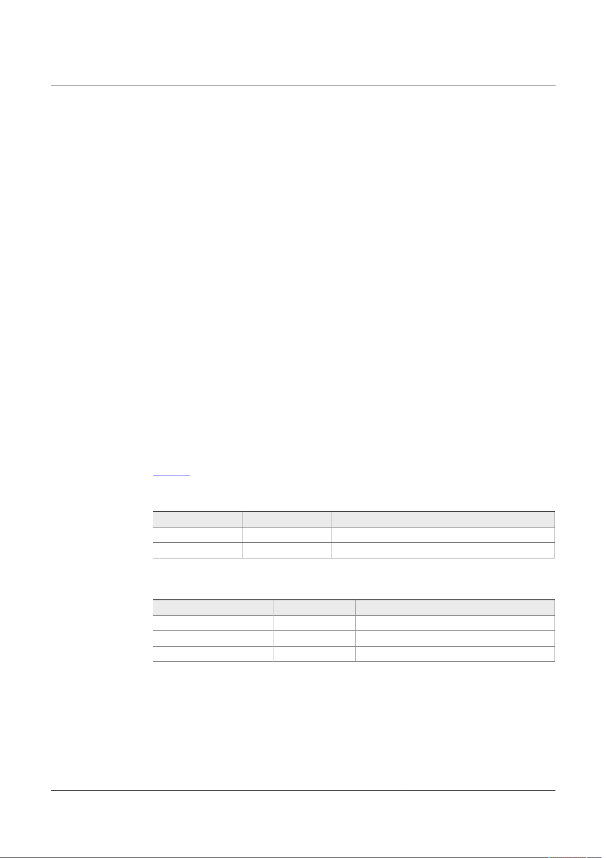
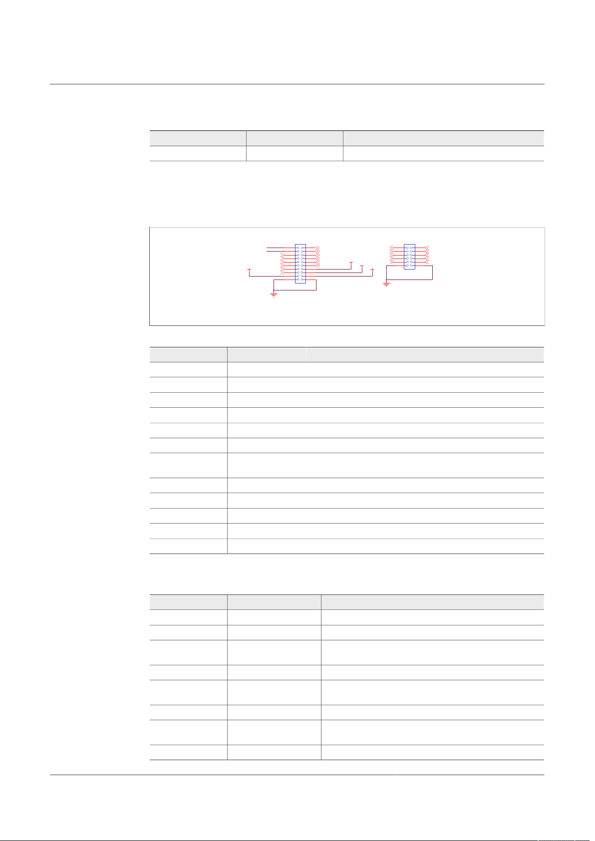
4.2.2 VBAT connectors
There are two ways of supplying the board: either by a Phoenix Connector (J2) or a Jack
connector (J2). The selection of the supplying connector is done using a three-position
switch (SW1).
Figure 3 shows related schematic. Nominal VBAT voltage is 12 V and can support up to
40 V.
Table 1. VBAT Phoenix connector (J1)
Schematic label Signal name Description
J1-1 VBAT Battery voltage supply input
J1-2 GND Ground
Table 2. VBAT three position connector (SW1)
Schematic label Signal name Description
SW1 pin 2-3 VBAT Phoenix Board supplied by Phoenix connector
SW1 pin 2 (middle position) VBAT Board not supplied
SW1 pin 2-1 VBAT jack Board supplied by Jack connector
UM11503 All information provided in this document is subject to legal disclaimers. © NXP B.V. 2021. All rights reserved.
User manual Rev. 1 — 29 January 2021
5 / 60
Page 6
NXP Semiconductors
aaa-039503
Vba
t
Vba
t
GND
GND
GND
GND
J21
1
2
3
SW1
1
2
3
S
1
S
2
J20
1
2
VBA
T
aaa-039505
For Boost
in
Back
En
d
For Boost
in Front
En
d (d
efa
ult)
VBST_PG_OUT
VBOOS
T
GND
GND
GND
GND
VBS
T
GND
GND
GND
VBST_BE_L
S
VBST_PG
VBST_FE_L
S
SJ7
Close
d
1
2
JP2
1
2
R11
1
0
C
1
10u
F
R
7
0.1
C12
22u
F
C
3
10u
F
Q18
NTR4101
DNP
1
3
2
SJ9
Close
d
1
2
D
1
PMEG045T100EP
D
1
2
3
L
6
4.7uH
LBST1
1
2
0.01u
F
DNPC103
R1080DN
P
Q19
BSS138LT1
G
DNP
1
2
3
R
2
0.0
2
JP5
1
2
C78
10u
F
C18
22u
F
R1090
R11
3
0
R10
2
510
K
DNP
0.01u
F
DNPC102
D
3
NRVTS245ESFT1
G
A
C
Q
1
NTD5C688N
L
1
3
4
C11
22u
F
G
S
D
Q
2
PMV30UN
2
C
2
10u
F
C
4
10u
F
C13
22u
F
R11
2
0
SJ8
Close
d
1
2
C94
10u
F
R10
1
510
K
DNP
SJ1
Close
d
1
2
R11
4
0
L
2
4.7uH
LBST2
1
2
VBST_BE_L
S
VBST_BE_I
N
VBST_G_BE
VBST_ISH_BE
VBST_ISL_BE
VBST_FE_I
N
VBST_OU
T
VBST_G_FE
VBST_ISH_FE
VBST_ISL_FE
VBOOST_SN
S
VBST_SN
S
Figure 3. VBAT connectors schematic
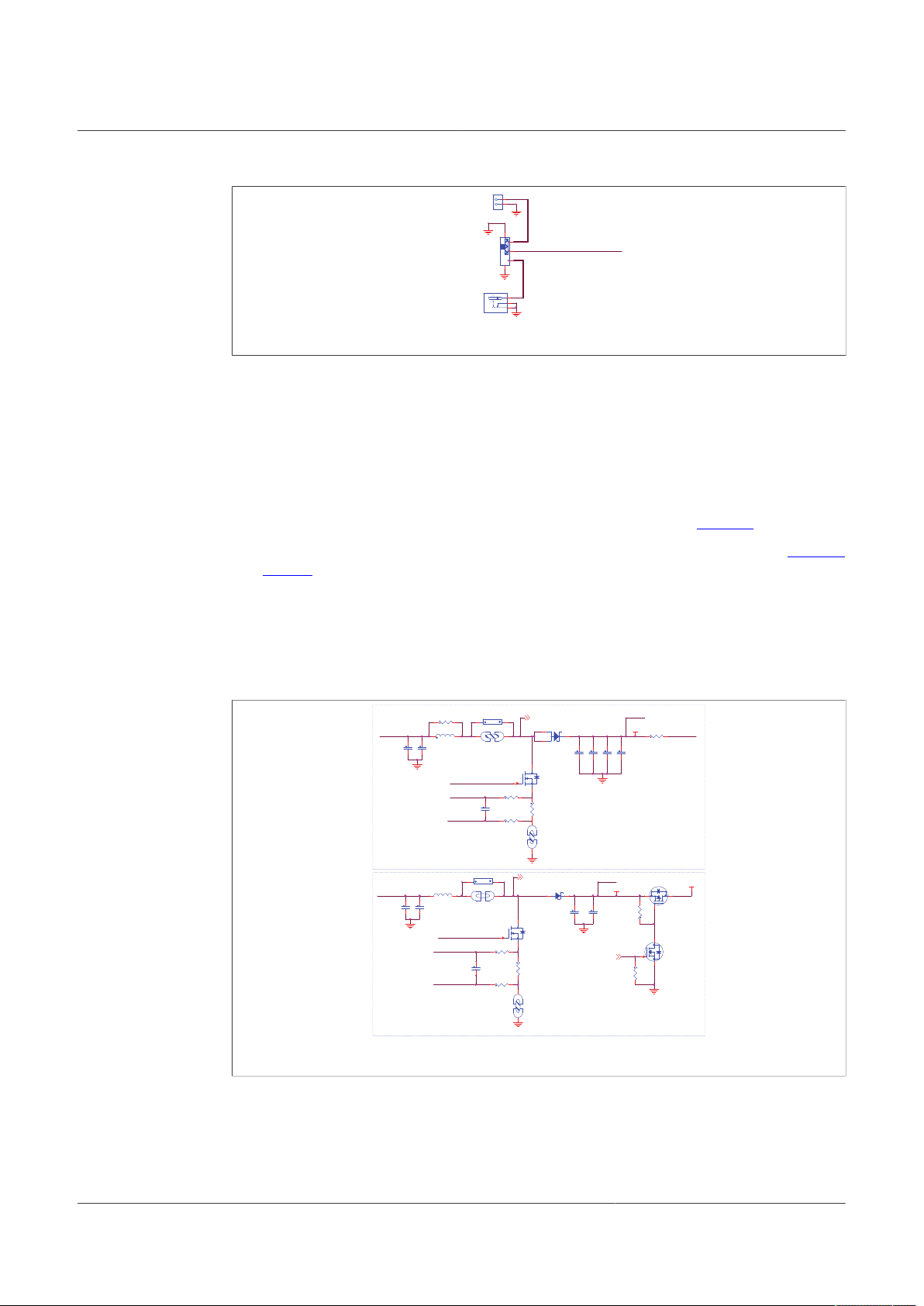
4.2.3 Power topology configuration
There are two power topologies available depending on the application and OTP
configuration. The device can be supplied directly by the battery after diode and pi filter;
on the other side, the boost regulator can be connected in front-end topology to support
cold cranking profiles.
It is possible to evaluate both power topologies with this board since external boost
components for each topology are soldered separately as shown in Figure 4.
A set of jumper configurations allows you to select between the two options. See Figure 5
and Table 3. Default jumper configuration is boost in front-end topology.
UM11503
KITFS26AEEVM evaluation board
In front-end topology boost is connected to the battery after reverse diode; the output
of the boost supplies the device during cold cranking profiles. Otherwise, boost stops
switching, and it is bypassed. See FS26 data sheet for more information.
In back-end topology or independent boost, the device is supplied by the battery, and the
boost is supplied by the buck regulator VPRE.
UM11503 All information provided in this document is subject to legal disclaimers. © NXP B.V. 2021. All rights reserved.
User manual Rev. 1 — 29 January 2021
Figure 4. Schematic of boost external components for front end and back-end topologies
6 / 60
Page 7
NXP Semiconductors
aaa-039511
ON:
BackEnd
OFF: FrontEnd
3-2: FrontEnd
1-2: BackEn
d
3-2: FrontEnd
1-2: BackEn
d
3-2: FrontEnd
1-2: BackEn
d
3-2: FrontEnd
1-2: BackEn
d
3-2: FrontEnd
1-2: BackEn
d
ON:
BackEnd
OFF: FrontEnd
3-2: FrontEnd
1-2: BackEn
d
J3VBST_BE_I
N
1
2
J5VSUP_PW
R
1
2
3
J6VBST_IS
H
1
2
3
J8VBST_IS
L
1
2
3
J7VSU
P
1
2
3
J26VBST_F
B
1
2
3
J25VBST_FE_IN
1
2
J4VBST_
G
1
2
3
VBST_
G
VBST_IS
H
VBST_IS
L
VSU
P
VBST_BE_I
N
VBST_G_FE
VBST_G_BE
VPR
E
VBST_OU
T
VBAT_
D
VSUP_PW
R
VPI
VBST_ISH_FE
VBST_ISH_BE
VBST_ISL_FE
VBST_ISL_BE
VBS
T
VPI
VBST_FE_I
N
VBST_SN
S
VBST_FB
VBOOST_SN
S
aaa-039512
VBA
T
Vsu
p
R
SNS_BST
C
OUT_BST
D
2
L
BST
1
D
1
C
IN_BS
T
FS26 SB
C
VBST_FE_I
N
VPI
Vsup_pw
r
Vpr
e
R
SNS_BST
C
OUT_BST
L
BST
2
D
3
C
IN_BS
T
R 0 Ohm
VBST_BE_I
N
VBS
T
VBST_OU
T
VBAT_
D
VBS
T
VPI
VBOOS
T
C
PRE_OUT
Vpre_SW
VBST_
G
VBST_IS
H
VBST_IS
L
VBST_G_BE
VBST_ISH_BE
VBST_ISL_BE
VBST_G_FE
VBST_ISH_FE
VBST_ISL_FE
VBST_G_FE
VBST_ISH_FE
VBST_ISL_FE
Cpi
1
Cpi
2
Lpi
J25
J
7
J
5
J
4
J
6
J
3
1
1
1
1
1
1
1
VBST_FB
VBS
T
1
VBOOS
T
Replace by
ferrite bead
if needed
Components for
BOOST in Front end
Components for
BOOST in Back end
Front end
topolog
y
Back end
topolog
y
L
1
VBAT_
D
J
8
J26
L
6
J
3
L
2
Q
2
Q
1
Figure 5. Boost configuration jumper section in the schematic
Table 3. Jumper configuration for front end and back-end power topologies
Schematic label Signal name BOOST front-end (default
J3 VBST_BE_IN OFF ON
J4 VBST_G 3-2 1-2
J5 VSUP_PWR 3-2 1-2
J6 VBST_ISH 3-2 1-2
J7 VSUP 3-2 1-2
J8 VBST_ISL 3-2 1-2
J25 VBST_FE_IN ON OFF
J26 VBST_FB 3-2 1-2
UM11503
KITFS26AEEVM evaluation board
BOOST back-end
positions)
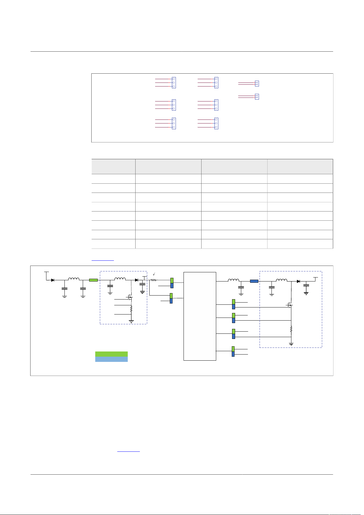
Figure 6 shows a simplified diagram of jumper configuration to associated device pins.
Figure 6. Simplified diagram of jumper configuration for front-end and back-end topologies
When testing the FS26 SBC with a front-end configuration at very low battery level and
loading product at its maximum rating, make sure that the power supply is capable of
providing at least 4.0 A.
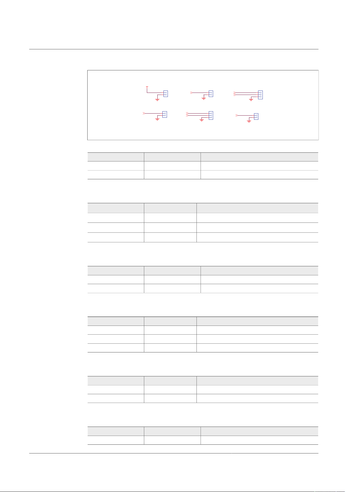
4.2.4 Output power supply connectors
UM11503 All information provided in this document is subject to legal disclaimers. © NXP B.V. 2021. All rights reserved.
User manual Rev. 1 — 29 January 2021
Output regulators are accessible through test points or Phoenix connectors in order to
make measurement or plug loads. Male connectors are included on this kit to plug or
unplug wires easily. All output regulators are located at the top edge of the board as
shown in Figure 2.
7 / 60
Page 8
NXP Semiconductors
aaa-039513
POWER OUTPUTS
VBOOS
T
GND
VCORE
GND
VTRK1
GND
VTRK2
VPRE
GND
VREF
GND
VLDO2
GND
VLDO1
GND
GND
GND
GND
GND
GND
VBOOS
T
VPR
E
VCORE
VLDO1
VLDO2
VTRK1
VTRK2
VRE
F
J15
1
2
3
J18
1
2
J19
1
2
J14
1
2
J17
1
2
3
J16
1
2
Figure 7. Power output Phoenix connectors
Table 4. VCORE connector (J14)
Schematic label Signal name Description
J16-1 VCORE VCORE power supply output
J16-2 GND Ground
Table 5. VTRK1/VTRK2 connector (J15)
Schematic label Signal name Description
J15-1 VTRK1 VTRK2 power supply output
J15-2 VTRK2 VTRK1 power supply output
J15-3 GND Ground
UM11503
KITFS26AEEVM evaluation board
Table 6. VPRE connector (J16)
Schematic label Signal name Description
J16-1 VPRE VPRE power supply output
J16-2 GND Ground
Table 7. VLDO1/VLDO2 connector (J17)
Schematic label Signal name Description
J17-1 LDO1 LDO1 power supply output
J17-2 LDO2 LDO2 power supply output
J17-3 GND Ground
Table 8. VREF connector (J18)
Schematic label Signal name Description
J18-1 VREF VREF reference output
J18-2 GND Ground
Table 9. VBOOST connector (J19)
Schematic label Signal name Description
UM11503 All information provided in this document is subject to legal disclaimers. © NXP B.V. 2021. All rights reserved.
User manual Rev. 1 — 29 January 2021
J19-1 VBOOST VBOOST power supply output
8 / 60
Page 9
NXP Semiconductors
aaa-039514
Signal connecto
r
Program connector
GND
GND
VSU
P
VDDIO
VBA
T
DBG_OTP
MOS
I
MIS
O
SCL
K
CSB
WAKE1_I
N
WAKE2_I
N
VDEBU
G
RST
B
INT
B
FS0
B
FS1
B
AMU
X
GPIO1
GPIO2
FCCU1
FCCU2
VMONEXT_0.8
V
GPIO1_I
N
GPIO2_I
N
VBAT_Ctrl
MCU_DBG8V
MCU_DBG5V
J11
HDR_2X6
1
2
3
4
6
5
7
8
910
111
2
J23
1
2
3
4
6
5
7
8
910
111
2
131
4
151
6
171
8
192
0
VMONEXT
VDDIO_EXT
Table 9. VBOOST connector (J19)...continued
Schematic label Signal name Description
J19-2 GND Ground
4.2.5 Signal and program connectors
Signal and program connectors allow access to most of the device signals in order to
program the device externally or to perform debug and diagnosis.
Figure 8. Signal and debug headers connectors
Table 10. Program connector (J11)
Schematic label Signal name Description
J11_1 WAKE1_IN WAKE1 input access
J11_2 MOSI MOSI signal access
J11_3 MISO MOSI signal access
J11_4 WAKE2_IN WAKE2 input access
J11_5 VDEBUG VDEBUG pin
J11_6 SCLK SCLK signal access
J11_7 VBAT_Ctrl VBAT_Ctrl KL25Z output access; to control VBAT power by MCU,
J11_8 CSB CSB signal access
J11_9 MCU_DBG8V MCU_DBG8V KL25Z output access
J11_10 MCU_DBG5V MCU_DBG5V KL25Z output access
J11_11 GND GND
J11_12 GND GND
UM11503
KITFS26AEEVM evaluation board
JP1 must be OFF
Table 11. Signal connector (J23)
Schematic label Signal name Description
J23_1 VMONEXT External monitoring, resistor bridge side
J23_2 RSTB RSTB IC safety output
J23_3 VDDIO_EXT Optional external supply for VDDIO, make sure that there is a
J23_4 INTB INTB interruption output
J23_5 GPIO1 GPIO1 IC side, for signal access; disconnect R87 before use
J23_6 FS0B FS0B IC safety output
J23_7 GPIO2 GPIO2 IC side, for signal access; disconnect R87 before use
J23_8 FS1B FS1B IC safety output
UM11503 All information provided in this document is subject to legal disclaimers. © NXP B.V. 2021. All rights reserved.
User manual Rev. 1 — 29 January 2021
jumper between J12 5-6 pins
as an output
as an output
9 / 60
Page 10
NXP Semiconductors
aaa-039515
LED SIGNALING
TRK
2
TRK
1
LDO
2
LDO
1
VRE
F
V
P
R
E
V
B
S
T
_
B
E
V
B
A
T
VCORE
GPIO1
GPIO2
V
B
S
T
_
F
E
VBA
T
GND
Vpr
e
Vpr
e
Vpr
e
Vpr
e
Vpr
e
VLDO1VLDO2VTRK1VTRK2VRE
F
GND
GND
GND
GND
GND
VBOOS
T
Vpr
e
GND
Vpr
e
GND
Vpr
e
GND
VBS
T
GPIO2
GPIO1
VPR
E
VCORE
R32510K
R23
1.3
K
R84
1.3
K
D14
A
C
D11
A
C
Q
3
1
2
3
R99510K
D24
A
C
R25
1.3
K
Q16
1
2
3
R31510K
D12
A
C
D23
A
C
R29
4.7
K
R27
4.7
K
R34510K
R95510K
D25
A
C
D13
A
C
R22
1.3
K
Q14
1
2
3
D10
A
C
R97510K
R30510K
Q15
1
2
3
R24
1.3
K
D22
A
C
D15
A
C
D
8
A
C
R85
1.3
K
R33510K
Q
4
1
2
3
R94
1.3
K
Q
5
1
2
3
SW4
SW_DIP-12/S
M
SWITCH(DEFAULT) = ALL O
N
12345109876
1516171819202122232
4
111
2
141
3
Q
6
1
2
3
R26
1.3
K
Q
7
1
2
3
R11
5
4.7
K
D
9
A
C
R28
1.3
K
V
B
A
T
_
L
E
D
VBST_FE
V
B
S
T
_
F
E
VBAT_LE
D
Table 11. Signal connector (J23)...continued
Schematic label Signal name Description
J23_9 FCCU1 FCCU1
J23_10 VMONEXT_0.8V VMONEXT IC side, for access or disconnect R39 to apply
J23_11 FCCU2 FCCU2
J23_12 AMUX AMUX pin read
J23_13 GPIO1_IN GPIO1 input side
J23_14 VDDIO VDDIO IC side access
J23_15 GPIO2_IN GPIO2 input side
J23_16 VSUP VSUP pin access
J23_17 DBG_OTP DBG_OTP power supply (8.0 V) access
J23_18 VBAT VBAT access
J23_19 GND GND
J23_20 GND GND
UM11503
KITFS26AEEVM evaluation board
0.8 V externally
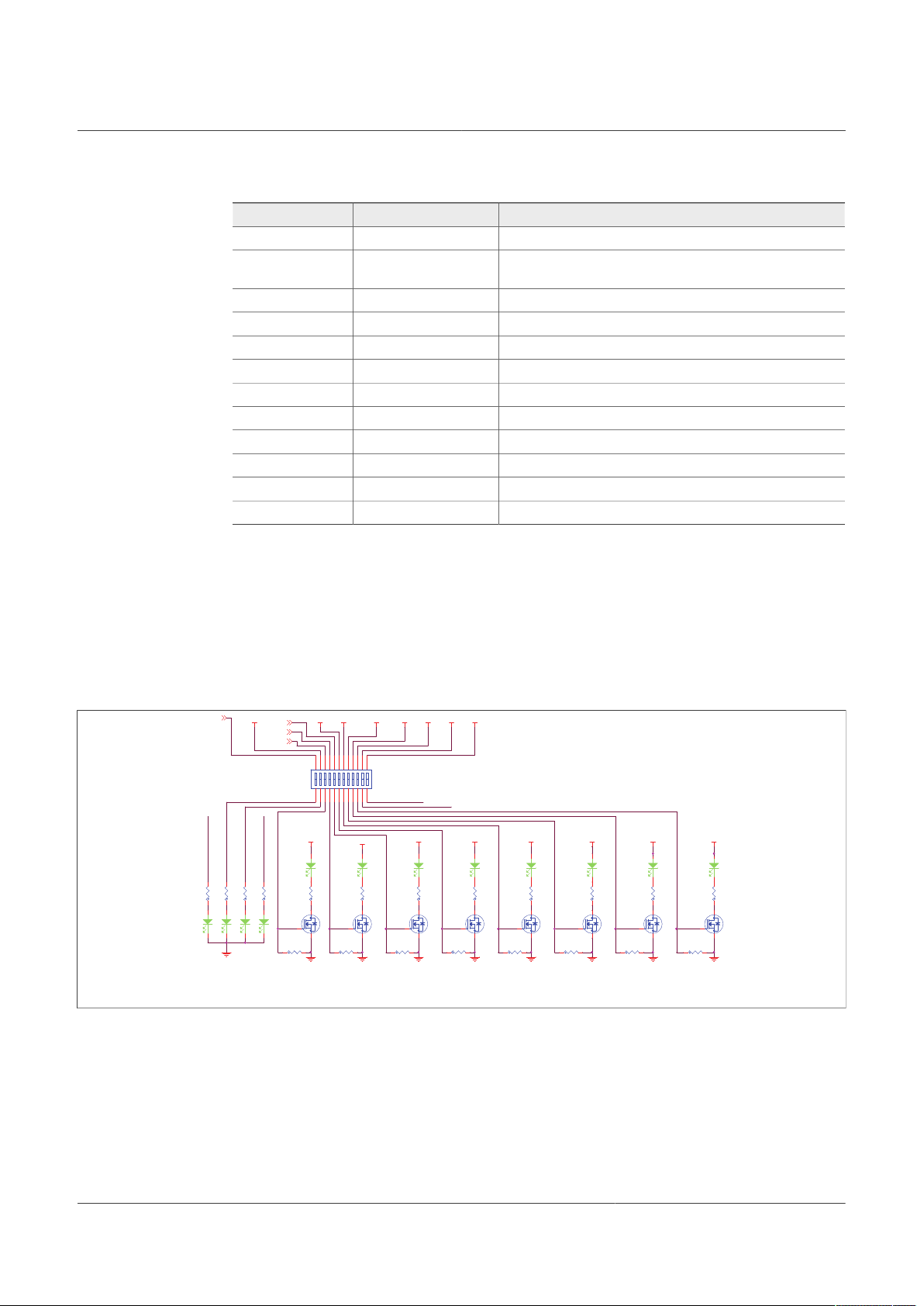
4.2.6 Indicators
The LED indicators on the board display VBAT regulators, safety outputs, and GPIO
status. For VBAT, regulators and GPIOs there are green LEDs indicating that the output
is powered on. The power supply of these indicators is usually VPRE, and it is controlled
by a low voltage MOSFET by the corresponding signal or regulator.
These regulators can be turned Off manually at any time with the switch SW4 in order to
avoid undesired losses and obtain more accurate current consumption measurements.
Figure 9. Power and regulator LED indicators
UM11503 All information provided in this document is subject to legal disclaimers. © NXP B.V. 2021. All rights reserved.
User manual Rev. 1 — 29 January 2021
10 / 60
LED indicators are turned On and Off when the safety output is released. LEDs can also
be disabled using switch SW5.
The color of the safety output LED indicators is red. When the safety output is asserted,
Page 11
NXP Semiconductors
aaa-039516
VDDIO
D
4
RED
A
C
R18
1.5
K
D
6
RED
A
C
R20
1.5
K
SW5
SW DIP-4/SM
123
4
876
5
R21
1.5
K
D
5
RED
A
C
R19
1.5
K
D
7
RED
A
C
RST
b
INT
B
FS0
b
FS1
b
aaa-039528
Debug
Through hole test point
s
TEST POINTS
Groun
d
Power
GND
GND
VBA
T
VSU
P
VPI
GND
GND
VDDIO
VBS
T
VBST_PG_OUT
VBOOS
T
GND
GND
VRE
F
VLDO1
FS0
B
VCORE
VLDO2
FS1
B
VPR
E
VTRK1
RST
B
VTRK2
INT
B
AMU
X
VBST_FE_L
S
VBST_BE_L
S
VPRE_SW
VCORE_S
W
VDEBU
G
VMONEXT_0.8
V
VBST_PG
VBO
S
TP7
BH1
MTG
1
TP4
4
TP1
1
TP3
4
TP2
5
TP3
2
BH3
MTG
1
TP3
5
TP3
0
TP2
8
TP2
0
TP1
5
TP4
1
TP1
6
TP3
6
TP2
7
TP4
2
TP1
9
BH2
MTG
1
TP2
2
TP1
8
TP5
TP1
4
TP2
6
TP1
0
BH4
MTG
1
TP4
3
TP1
2
TP2
1
TP8
TP1
7
TP6
TP1
3
TP2
4
TP9
TP2
3
Figure 10. Safety output LED indicators
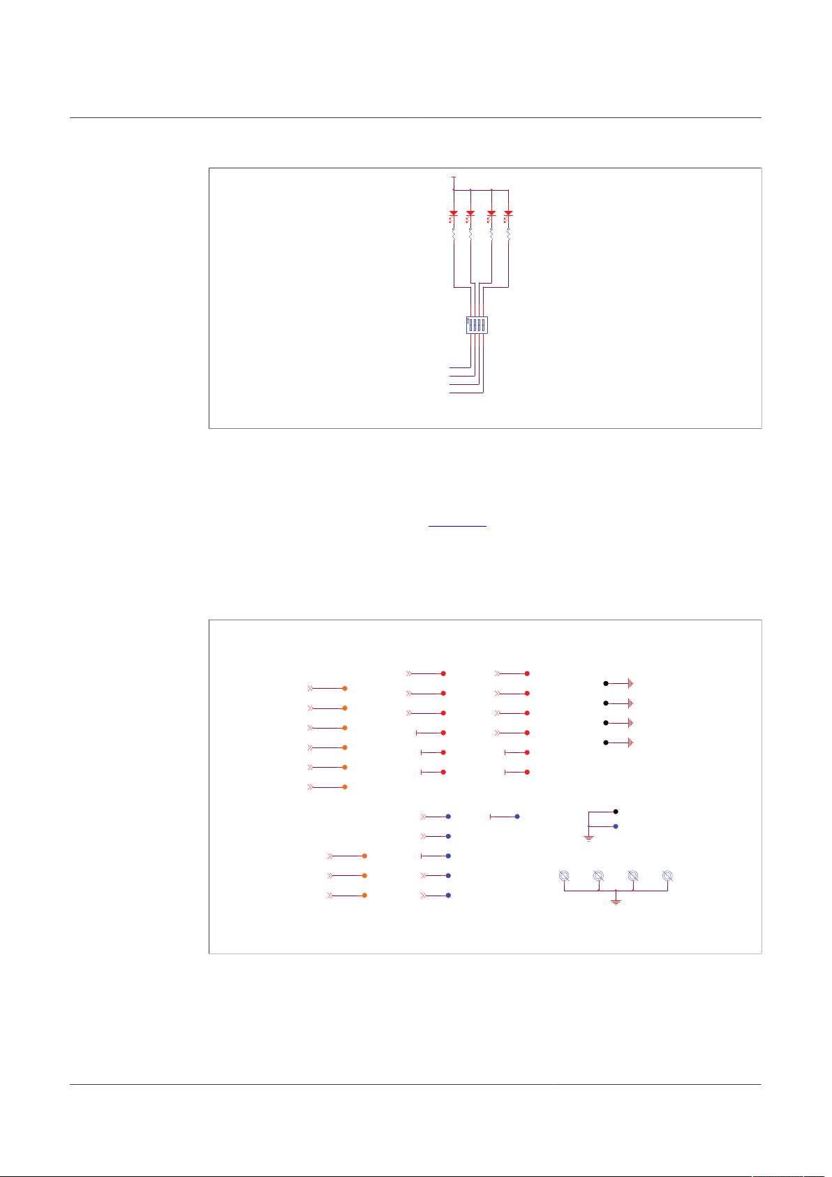
4.2.7 Test points
The KITFS26AEEVM evaluation board has several test points for easy access and
measurements. The test points are color coded, and can be different part numbers or
without a part number, as shown in Figure 11.
UM11503
KITFS26AEEVM evaluation board
• Orange: test loop access to safety outputs and analog signals
• Red: test loop access for power supplies
• Black: test loop access to GND
• Blue: not a part; through hole small test points on board close to the signal
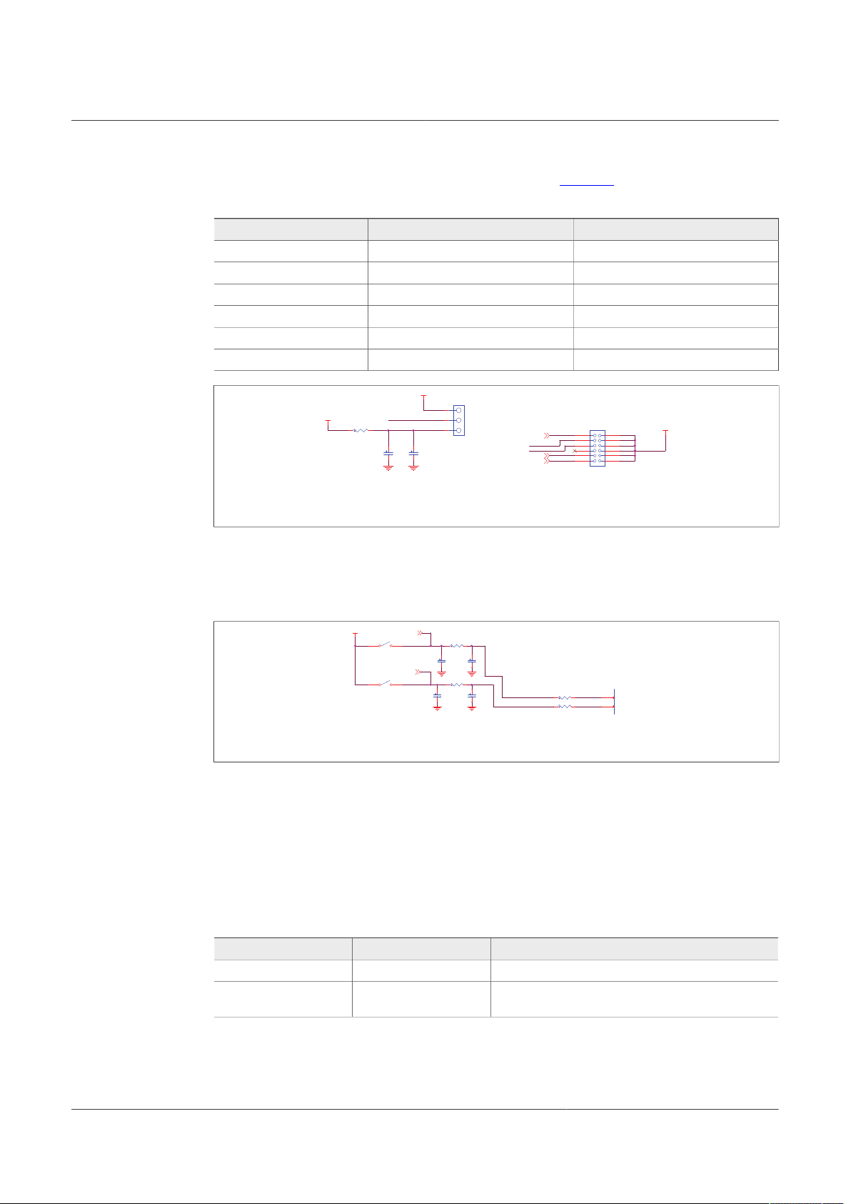
4.2.8 VDDIO selection
UM11503 All information provided in this document is subject to legal disclaimers. © NXP B.V. 2021. All rights reserved.
User manual Rev. 1 — 29 January 2021
Figure 11. KITFS26AEEVM test points
VDDIO reference can be supplied by 3.3 V or 5.0 V depending on the system. The
supply can be generated on the board, from a voltage regulator, or from an external
source.
11 / 60
Page 12
NXP Semiconductors
aaa-039529
GNDGN
D
VDDIO
P3V3_KL25
Z
P5V_KL25Z
VCORE
VLDO1
VLDO2
C30
1.0UF
DNP
R36
0
C31
1.0UF
DNP
J22
1
2
3
J12
HDR_2X6
1
2
3
4
6
5
7
8
910
111
2
VDDIO_USB
VDDIO_EXT
VDDIO_USB
aaa-039530
VBA
T
GNDGN
D
GND
GND
WAKE1_I
N
WAKE2_I
N
5.1
K
R
6
R55.1
K
0.01u
F
C15
DNP
0.01u
F
C17
SW2
1
2
SW3
1
2
WAKE2
2
WAKE1
4
7
0.022uF
C14
R86
0.022uF
C16
R35.1
K
5.1
K
R
4
WAKE1
WAKE2
WAKE1_I
N
WAKE2_I
N
J12 allows selection of the supply source, as shown in Table 12.
Table 12. VDDIO connector (J12)
Schematic label Signal name Description
J12_1-2 VCORE VDDIO supply is VCORE
J12_3-4 (default) VDDIO_USB VDDIO supply is VDDIO_USB (J22_2)
J12_5-6 VDDIO_EXT VDDIO supply is VDDIO_EXT (J23_3)
J12_7-8 NC VDDIO Not connected
J12_9-10 VLDO1 VDDIO supply is VLDO1
J12_11-12 VLDO2 VDDIO supply is VLDO2
UM11503
KITFS26AEEVM evaluation board
Figure 12. VDDIO source selector headers
4.2.9 Wake input switches
Wake inputs can be exercised by switches SW2 for WAKE1_IN and SW3 for WAKE2_IN.
These interrupts are supplied by the battery to VBAT signal.
Figure 13. WAKE pins control switches
4.2.10 VDEBUG pin voltage control
VDEBUG pin allows FS26 SBC to enter the different operating modes to perform debug
or programming by applying different voltage thresholds or sequences. These thresholds
can be generated on the board and debug pin can be controlled manually or fully
automated by KL25Z.
The selection for manual (default) or automatic is done by J13.
Table 13. Debug control selector (J13)
Schematic label Signal name Description
J13_1-2 Manual (default) Debug thresholds are control by SW6 and SW7
J13_2-3 Automatic (feature not
enabled)
Debug thresholds are controlled by KL25Z
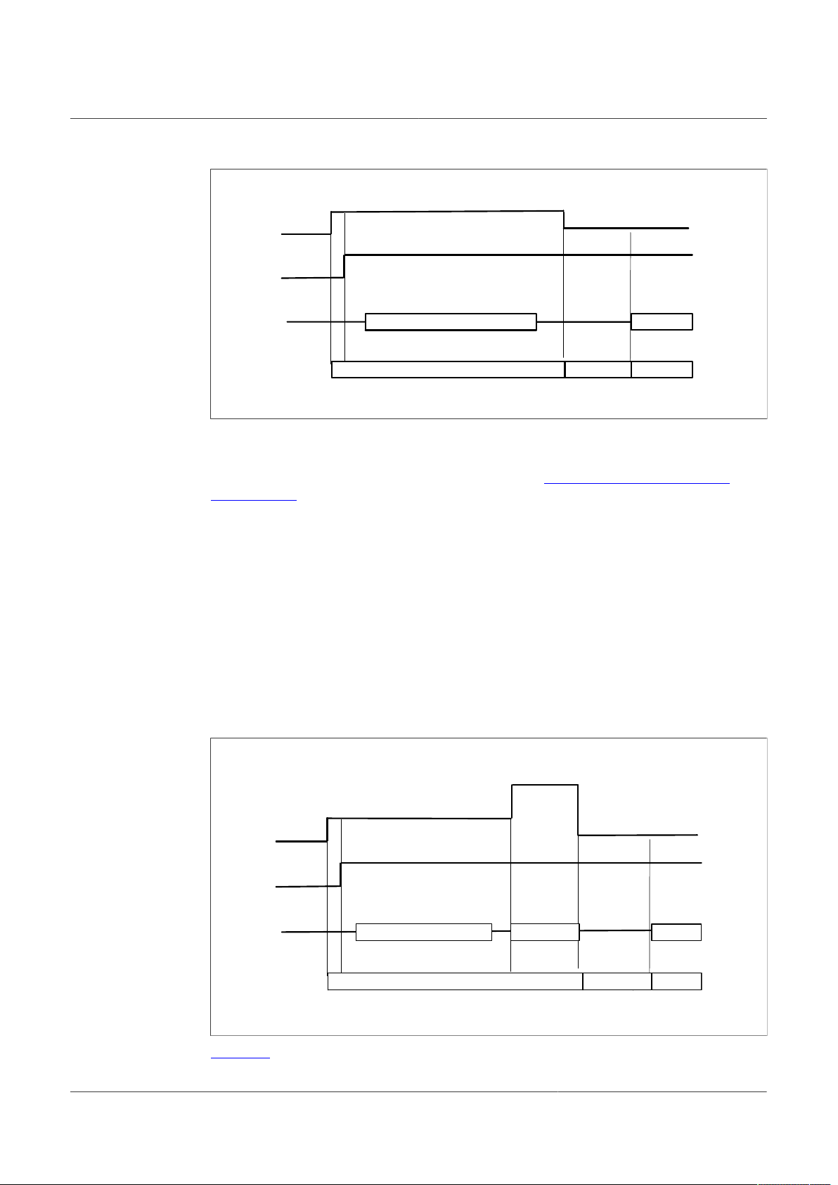
Different voltage levels and sequences can be used to enter Debug mode; emulate an
OTP configuration, or burn an OTP configuration to the fuses. The threshold levels are:
12 / 60
UM11503 All information provided in this document is subject to legal disclaimers. © NXP B.V. 2021. All rights reserved.
User manual Rev. 1 — 29 January 2021
Page 13
NXP Semiconductors
• VDEBUG < VDBG4TH (VDEBUG < 4.2 V): waive debug entry at power up or after low-
power modes exit.
• VDEBUG > VDBG4TH (VDEBUG > 4.2 V): enter debug mode at power up or after low
power modes exit.
• VDEBUG VDBG65TH (VDEBUG > 6.9 V): burning level for OTP programming.
The power supply to generate the debug entry voltage threshold comes from KL25Z
USB. This means that Freedom board and USB must be plugged in. Burning voltage for
OTP is generated by an onboard boost IC that is also powered by FRDM-KL25Z.
For manual mode, use SW6 to allow connection to 5.0 V power supply, and SW7 to
connect to 8.0 V power supply; when VDBG65TH is reached a blue LED (D19) turns On.
Table 14 shows the possible output voltage level to apply to VDebug pin depending on
SW6 and SW7 positions.
Table 14. SW6 and SW7 VDebug output configuration
SW6 SW7 VDebug (J13-2) voltage level
OFF OFF 0 V
OFF ON 7.8 V
ON OFF 4.5 V
ON ON 7.8 V
UM11503
KITFS26AEEVM evaluation board
When automatic mode is selected on connector J13 and KL25Z is plugged in and used,
5.0 V and 8.0 V thresholds can be controlled on the NXP GUI by KL25Z signals. It is also
possible to control VBAT by a MCU signal to generate automated sequences for program
and emulations; these signals are:
VBAT_Ctrl: Open or close VBAT power supply
MCU_DBG5V: 5.0 V on VDEBUG pin
MCU_DBG8V: 8.0 V on VDEBUG pin
Debug mode entry
To enter debug mode, follow the sequence:
1. VBAT Off (SW1)
2. VDebug (J13) > VDBG4TH
3. VBAT On (SW1)
4. At this step Debug mode is enabled and you can emulate an OTP configuration or
access the SPI register map. You can read FS_STATES register to verify you are in
Debug mode.
UM11503 All information provided in this document is subject to legal disclaimers. © NXP B.V. 2021. All rights reserved.
User manual Rev. 1 — 29 January 2021
13 / 60
Page 14
NXP Semiconductors
aaa-039531
VSU
P
>
V
SUP_UVH
DEBUG
V
Debug
= 5 V
SPI or OTP Emulatio
n
SPI
OFF
REG
x
O
N
PWR U
P
SPI
V
Debug
= 0
V
Debug entry/Emulation
V
Debug
= 5 V
V
Debug
= 0
V
V
Debug
= 8
V
VSU
P
>
V
SUP_UVH
DEBUG
SPI OTP program
SPI
OFF
REG
x
O
N
PWR U
P
SPI
OTP programming
Go CM
D
aaa-039532
Figure 14. Debug entry voltage sequence
OTP programming
To burn an OTP configuration on the fuses permanently, the following sequence must
be applied. More detailed instructions are provided in Section 8.5 "Program an OTP
configuration".
UM11503
KITFS26AEEVM evaluation board
1. VBAT OFF (SW1)
2. VDebug (J13) > VDBG4TH (SW6 On).
3. VBAT On (SW1)
4. At this step, Debug mode is enabled and you can emulate an OTP configuration or
access the SPI register map. You can read FS_STATES register to verify you are in
Debug mode.
5. VDebug (J13) > VDBG65TH (SW7 On). If the threshold is applied, D19 blue LED
turns On.
6. Load an OTP configuration file and wait until all commands are sent.
7. Put VDebug (J13) to 0 V (first SW7, and then SW6).
8. The device should power up with selected OTP configuration or you can restart the
device power supply to load the burned OTP configuration from fuses.
Figure 15. OTP programming voltage sequence
Figure 16 shows the VDebug voltage sources and its selection.
UM11503 All information provided in this document is subject to legal disclaimers. © NXP B.V. 2021. All rights reserved.
User manual Rev. 1 — 29 January 2021
14 / 60
Page 15
NXP Semiconductors
aaa-039533
DEBUG & PROG VOLTAG
E
Burning
Volt
age
(on DBG pin)
RH1
to be replaced by 53.6k for DBG_OTP = 8V or solution to be replace
d
J13
1-2: Manual
3-2: Auto
GND
P3V3_KL25
Z
GND
GND
GND
GND
P3V3_KL25
Z
P3V3_KL25
Z
GND
GND
GND
GND
DBG_OTP
GND
GND
P5V_KL25Z
MCU_DBG5V
VDEBU
G
MCU_DBG8V
VDEBU
G
LT1618EMS
U
2
F
B
1
I
S
N
2
ISP
3
I
A
D
J
4
G
N
D
5
N
C
6
S
W
7
VIN
8
SHD
N
9
V
C
1
0
D16
BAT46ZFIL
M
A
C
-
+
VDD
VSS
U
4
MCP6001T-E/OT
3
1
4
5
2
C34
4.7uF
R4710
K
R35
510
K
C37
1.0UF
Q10
FDN360P
1
3
2
R4480.6
K
C36
10n
F
R4810
K
Q11
BSS138LT1
G
1
2
3
C32
4.7uF
R410.
1
D19BLUE
A
C
J13
1
2
3
R45
3.3
K
R82
510
K
Q
8
BSS138LT1
G
1
2
3
R43
19.6K
R83
47K
D17PMEG2005AE
L
A
C
Q
9
FDN360P
1
3
2
R38
47K
R4622.1
K
R91
10K
RL1
D18
BAT46ZFIL
M
A
C
C38
0.1uF
SW6
1
2
R90
52.3K
1
%
RH1
L310u
H
1
2
SW7
1
2
P5V_KL25Z
DBG_OTP
P5V_KL25Z
DBG_OTP
aaa-039534
GND
VMONEXT_0.8
V
R37
100
K
1
3
2
R40
22.1K
R39
0
VMONEXT
UM11503
KITFS26AEEVM evaluation board
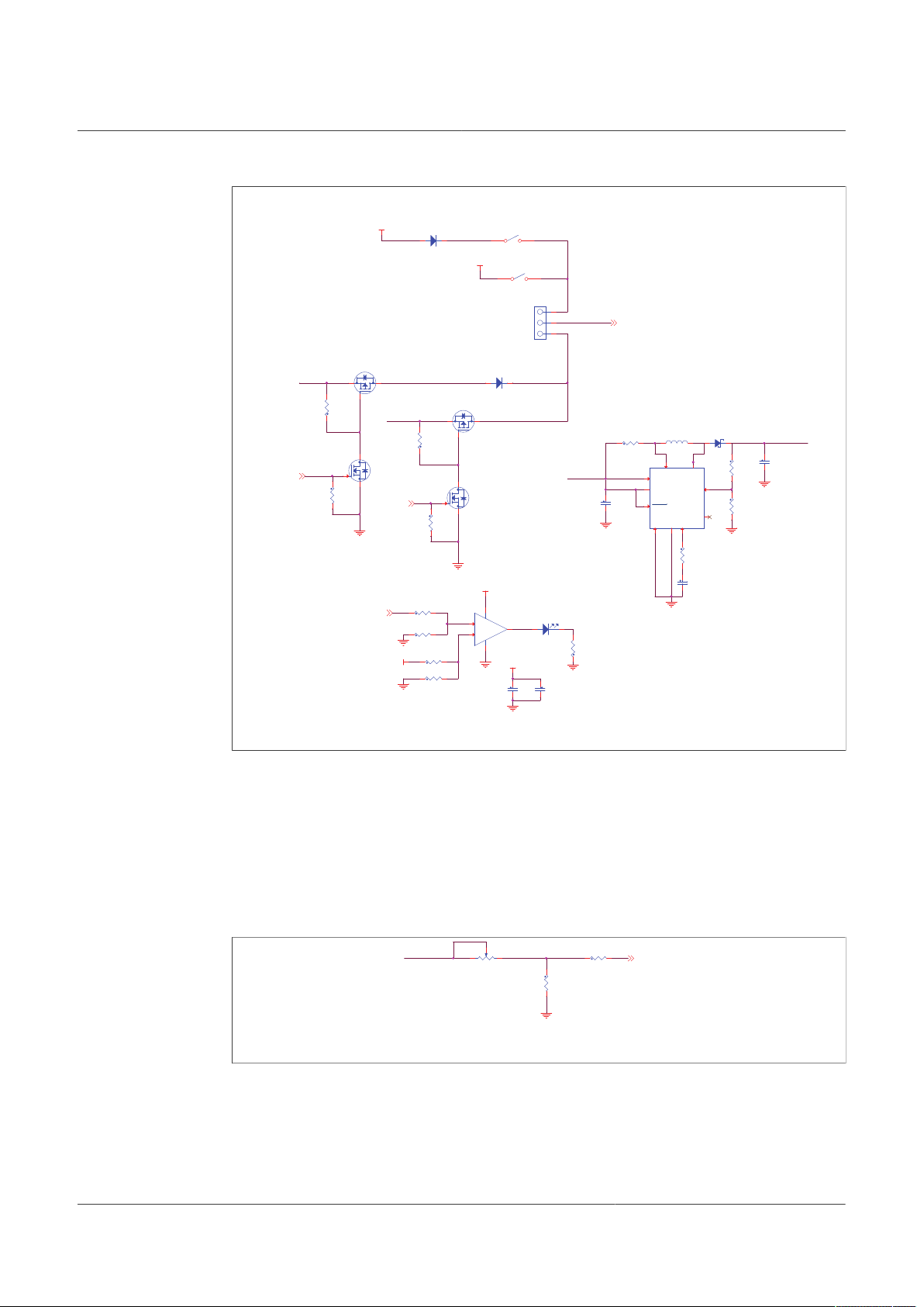
Figure 16. VDEBUG pin source selection schematic
4.2.11 VMONEXT monitoring
UM11503 All information provided in this document is subject to legal disclaimers. © NXP B.V. 2021. All rights reserved.
User manual Rev. 1 — 29 January 2021
4.2.12 GPIO1 and GPIO2
FS26 VMONEXT monitoring pin can be accessed in different ways. If used, VMONEXT
value should always be 0.8 V. VMONEXT signal can be supplied by any source or
regulator and VMONEXT_0.8V value can be adjusted by using a screwdriver on R37
potentiometer. Default bridge resistor is 22.2 kΩ.
To apply 0.8 V directly to VMONEXT_0.8V, remove R39 and apply 0.8 V to connector
J23_1.
Figure 17. VMONEXT voltage resistor bridge schematic
GPIO1 and GPIO2 FS26 pins are connected by default as outputs, and can be accessed
by J23 connector.
• J23_5 for GPIO1
15 / 60
Page 16

NXP Semiconductors
aaa-039535
GNDGN
D
GND
GND
GND
GND
GPIO1_I
N
GPIO2_I
N
0.01u
F
C80
0.01u
F
C82
5.1
K
R88
R875.1K
DNP
0.022uF
C79
0.022uF
C81
GPIO1
3
GPIO2
6
R89
5.1KDNP
5.1
K
R86
GPIO1
GPIO2
• J23_7 for GPIO2
To exercise GPIO pins as inputs, R87 and R89 must be populated in order to apply
voltage before RC filter. GPIO input supply can be applied through J23 header.
• GPIO1_IN can be accessed through J23_13; R87 must be populated.
• GPIO2_IN can be accessed through J23_15; R89 must be populated.
Figure 18. GPIO1 and GPIO2 schematics
Note: There are no external pull-ups or pull-downs for the GPIO. If the internal pull-ups
or pull-downs are not enabled by OTP, external PU/PD can be added through J23.
4.3 Schematic, board layout and bill of materials
The schematic, board layout and bill of materials for the KITFS26AEEVM evaluation
board are available at http://www.nxp.com/KITFS26AEEVM.
UM11503
KITFS26AEEVM evaluation board
5 Installing and configuring software and tools
5.1 Flashing or updating the GUI firmware
The KITFS26AEEVM is delivered with the GUI firmware flashed. If MCU firmware is
flashed, ignore this section. If it is specified to update the firmware or it is malfunctioning,
follow the instructions in Section 5.1.1 "Flashing Freedom board firmware for Windows 7"
and Section 5.1.2 "Flashing Freedom board firmware from Windows 10".
5.1.1 Flashing Freedom board firmware for Windows 7
Steps 1 and 2 are not required if BOOTLOADER is already loaded in the Freedom board.
1. Press the RST push-button and connect the USB cable into the SDA port on the
Freedom board.
• A new “BOOTLOADER” device should appear on the left pane of the File explorer.
2. Drag and drop the file “MSD-DEBUG-FRDM-KL25Z_Pemicro_v118.SDA” into the
BOOTLOADER drive.
Note: Make sure to allow enough time for the firmware to be saved in the Bootloader.
3. Disconnect and reconnect the USB cable into the SDA port.
• This time without pressing the RST push-button, FRDM_KL25Z device should
appear on the left pane of the File explorer.
UM11503 All information provided in this document is subject to legal disclaimers. © NXP B.V. 2021. All rights reserved.
User manual Rev. 1 — 29 January 2021
16 / 60
Page 17
NXP Semiconductors
4. Locate the file “nxp-gui-fw-frdmkl25z-usb_hid-fs2630_vX.Y.bin” from the package and
drag and drop the file into the FRDM_KL25Z device.
Note: Make sure to allow enough time for the firmware to be saved.
5. Freedom board firmware is successfully loaded. Disconnect and reconnect the USB
cable into the KL25Z USB port.
5.1.2 Flashing Freedom board firmware from Windows 10
1. Disable the storage services: run the services, double-click on the storage service
from the list and press STOP.
UM11503
KITFS26AEEVM evaluation board
Steps 2 and 3 are not required if BOOTLOADER is already loaded in the Freedom
board.
2. Press the RST push-button and connect the USB cable into the SDA port on the
Freedom board.
a. A new “BOOTLOADER” device should appear on the left pane of the File explorer.
3. Drag and drop the file “MSD-DEBUG-FRDM-KL25Z_Pemicro_v118.SDA” into the
BOOTLOADER drive.
Note: Make sure to allow enough time for the firmware to be saved in the
BOOTLOADER.
4. Disconnect and reconnect the USB cable into the SDA port.
• This time without pressing the RST push-button, FRDM_KL25Z device should
appear on the left pane of the File explorer.
5. Locate the file “nxp-gui-fw-frdmkl25z-usb_hid-fs2630_vX.Y.bin” from the package and
drag and drop the file into the FRDM_KL25Z device.
Note: Make sure to allow enough time for the firmware to be saved.
6. Freedom board Firmware is successfully loaded. Disconnect and reconnect the USB
cable into the KL25Z USB port.
UM11503 All information provided in this document is subject to legal disclaimers. © NXP B.V. 2021. All rights reserved.
User manual Rev. 1 — 29 January 2021
17 / 60
Page 18
NXP Semiconductors
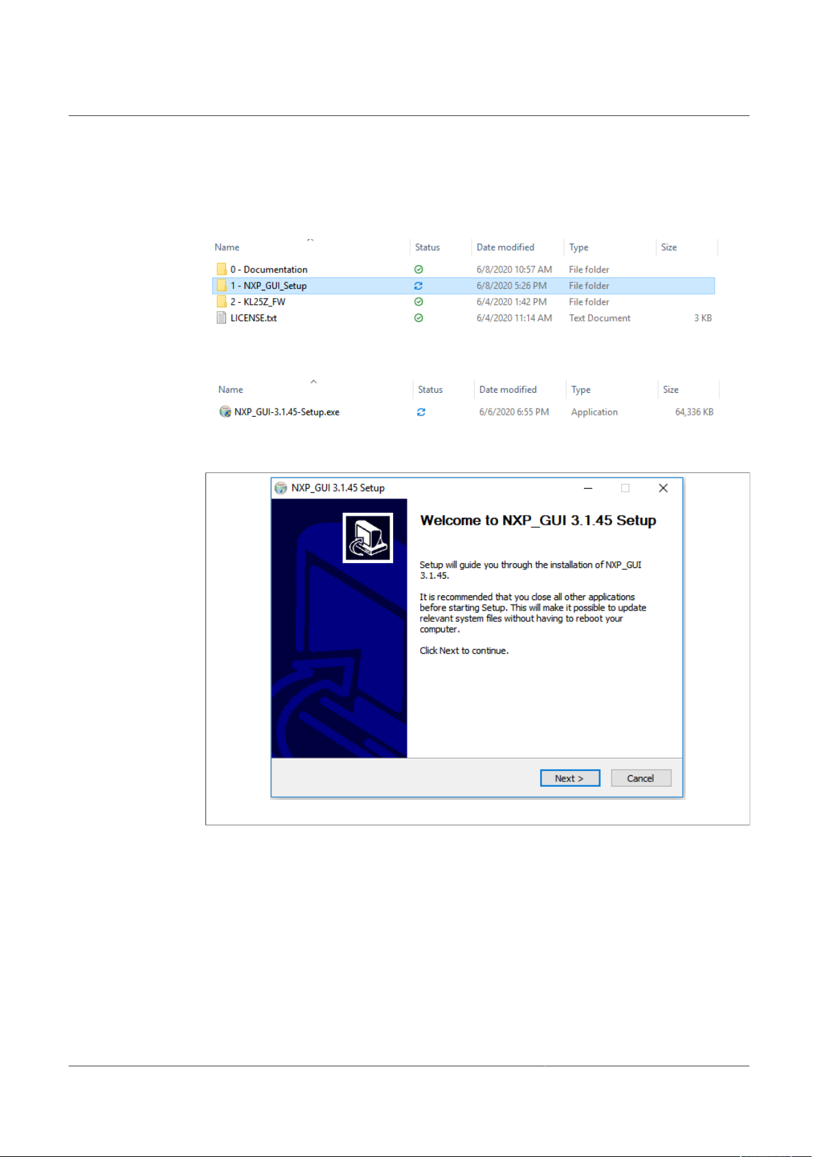
5.2 Installing GUI software package
To install the FS26 NXP GUI, download or obtain the NXP GUI package, unzip 1NXP_GUI_Setup folder:
Double-click NXP_GUI_version-Setup.exe and follow the instructions.
Proceed with the following pop-up windows to install the application on Windows PC:
UM11503
KITFS26AEEVM evaluation board
Figure 19. Application setup
UM11503 All information provided in this document is subject to legal disclaimers. © NXP B.V. 2021. All rights reserved.
User manual Rev. 1 — 29 January 2021
18 / 60
Page 19

NXP Semiconductors
UM11503
KITFS26AEEVM evaluation board
Figure 20. License agreement
Figure 21. Select FS2630_GUI feature
UM11503 All information provided in this document is subject to legal disclaimers. © NXP B.V. 2021. All rights reserved.
User manual Rev. 1 — 29 January 2021
19 / 60
Page 20

NXP Semiconductors
UM11503
KITFS26AEEVM evaluation board
Figure 22. Choose the folder to install
Select the following options before completing the installation of the setup:
• Run NXP_GUI
• Show Readme
Select Finish to complete the installation.
Figure 23. Run NXP_GUI
When installation is finished the application can be found in the windows search bar as
“NXPGUI”.
UM11503 All information provided in this document is subject to legal disclaimers. © NXP B.V. 2021. All rights reserved.
User manual Rev. 1 — 29 January 2021
20 / 60
Page 21

NXP Semiconductors
6 Configuring the hardware
UM11503
KITFS26AEEVM evaluation board
Figure 24. Typical initial configuration
To configure the hardware and workstation, complete the following procedure:
1. With SW1 in middle position, set DC power supply to 12 V and current limit to 1.0 A.
Attach the DC power supply positive and negative output to KITFS26AEEVM VBAT
Phoenix connector(J1). Or connect 12 V power supply to VBAT Jack (J2).
Table 15. VBAT Phoenix connector (J1)
Schematic label Signal name Description
J1-1 VBAT Battery voltage supply input
J1-2 GND Ground
Table 16. VBAT three position connector (SW1)
Schematic label Signal name Description
SW1 pin 2-3 VBAT Phoenix Board supplied by Phoenix connector
SW1 pin 2 (middle position) VBAT Board not supplied
SW1 pin 2-1 VBAT jack Board supplied by Jack connector
2. Connect the Windows PC USB port to the KL25Z USB side of the freedom board
included in the kit, using the provided USB 2.0 cable.
3. Turn On SW6 to apply 5.0 V to the VDebug pin.
4. Turn On the power supply.
5. Close SW1.
UM11503 All information provided in this document is subject to legal disclaimers. © NXP B.V. 2021. All rights reserved.
User manual Rev. 1 — 29 January 2021
21 / 60
Page 22

NXP Semiconductors
Note: At this step, the product is in debug mode and all regulators are turned Off. The
user can then power up with OTP configuration or configure the mirror registers before
power up. Power up is effective as soon as SW6 is turned Off.
7 FS26 NXP GUI
Once the kit is ready and the NXP GUI is installed, launch the kit from the Windows
search bar.
Launching FS26_GUI application
1. When the NXP GUI is launched, the Kit Selection window is displayed. Check for the
following settings and then select OK.
UM11503
KITFS26AEEVM evaluation board
2. To avoid the kit selection window on every launch, select the box “Use this
configuration and do not ask again”.
The following window is displayed.
UM11503 All information provided in this document is subject to legal disclaimers. © NXP B.V. 2021. All rights reserved.
User manual Rev. 1 — 29 January 2021
22 / 60
Page 23

NXP Semiconductors
7.1 Framework
UM11503
KITFS26AEEVM evaluation board
Device manager: Start communication with device. Enter or exit test mode. Quick
access to execute system scripts.
Framework settings: Import or export files, configure framework.
Window log: USB and Device communication events.
USB and device status: Displays if USB or Device is connected or disconnected.
Displays firmware and GUI version. Display current state of FS state machine; click
Display to refresh.
Tool access bar: Quick access to the FS26 evaluation tools and features.
UM11503 All information provided in this document is subject to legal disclaimers. © NXP B.V. 2021. All rights reserved.
User manual Rev. 1 — 29 January 2021
23 / 60
Page 24

NXP Semiconductors
Tab content: Content of each tool or tab; there can be more tabs, boxes, or windows
inside.
7.1.1 Framework settings
The NXP GUI main menu has five GUI elements: File, View, Export, NXP, and Help.
7.1.1.1 File
Load or save a configuration or exit the application. Load and save are only enabled
when OTP tool tab is active.
UM11503
KITFS26AEEVM evaluation board
• Load: Loads an existing configuration file previously exported from OTP tool to
continue to modify it on the OTP tool. This file has a .cfg extension. It is identified as:
FS26_ProgIDASILlevel_CONFIG.cfg.
Example: FS26_A0D_CONFIG.cfg.
• Save: Saves the current configuration of the OTP tool as a .cfg file.
• Use default configuration: Loads default values into the OTP tool.
• Exit: Exits NXP GUI application
7.1.1.2 View
This main menu has options related to GUI display.
• Display
• Show
• Naming Conventions
Display: It consists of Connection Tool Bar (enabled by default) option. To show or hide,
go to View → Display, and then select Connection Tool Bar.
Figure 25. Display options
Show: This option can be used to access various sections of the GUI.
UM11503 All information provided in this document is subject to legal disclaimers. © NXP B.V. 2021. All rights reserved.
User manual Rev. 1 — 29 January 2021
24 / 60
Page 25

NXP Semiconductors
Figure 26. Show options
Naming Conventions: Select Friendly or Register name display for OTP tool. Option
enabled only when OTP tool is active.
UM11503
KITFS26AEEVM evaluation board
Figure 27. Naming conventions options
Friendly: Go to View → Naming Conventions → Friendly. This mode helps to view the
registers names as user-friendly names throughout the OTP tool.
Figure 28. Friendly mode
UM11503 All information provided in this document is subject to legal disclaimers. © NXP B.V. 2021. All rights reserved.
User manual Rev. 1 — 29 January 2021
25 / 60
Page 26

NXP Semiconductors
Register: Go to View → Naming Conventions → Register. This mode helps to view the
register names as register's technical names throughout the OTP Tool.
Example: VSUP UV threshold → VSUP_UVTH_OTP
7.1.1.3 Export
This option allows user to export the current OTP from the OTP tool into different script
formats.
• OTP: Exports OTP configuration into OTP script file for programming.
• TBB: Exports OTP configuration into a TBB script file for emulation
• I-HEX: Exports to Intel Hex script file
• S-HEX: Exports to Simple Hex script file
UM11503
KITFS26AEEVM evaluation board
Figure 29. Export options
This option is enabled only in OTP Tool and remains disabled in other sections of the
GUI.
7.2 Device manager
The device manager allows start/stop of communication with device as well as enter/exit
of the test mode; it also allows quick access to execute useful system scripts.
Figure 30. Device manager
7.2.1 Device connection
If USB is detected from USB and device status bar, the USB status changes from NOT
DETECTED to DISCONNECTED. Start button is enabled.
Click Start to initiate communication with FS26 device.
UM11503 All information provided in this document is subject to legal disclaimers. © NXP B.V. 2021. All rights reserved.
User manual Rev. 1 — 29 January 2021
26 / 60
Page 27

NXP Semiconductors
When connected successfully, FS26 color changes to green and other buttons are
enabled. USB status changes to CONNECTED.
Apply test mode to send Main and Fail-safe Test mode entry keys. If test mode is entered
correctly, button changes to “Exit test mode”.
When test mode is entered, options requiring test mode are enabled, such as Mirrors and
device programming.
UM11503
KITFS26AEEVM evaluation board
Click Polling to do a continuous check of test mode entry.
If the device versioning bits are already programmed with an existing part number, the
NXP GUI decodes and displays the assigned Device ID. The following example displays
FS2633D.
7.2.2 Script shortcuts
To find a section with system script shortcuts, select the script and click execute. This
does not warrant the entry or acknowledge of the device. Device must be in INIT FS
state in most cases.
7.3 Access
7.3.1 Register map
The register access tab allows read/write to the FS26 Main and Fail-safe register maps
and is divided into following sections:
UM11503 All information provided in this document is subject to legal disclaimers. © NXP B.V. 2021. All rights reserved.
User manual Rev. 1 — 29 January 2021
27 / 60
Page 28

NXP Semiconductors
• Functional: Main functional SPI registers (diagnostics, configuration, and controls)
• Safety: Safety SPI registers (diagnostics and configuration)
• Write_INIT_Safety: Safety registers that can be configured during INIT FS state (for
example, WD configuration and WD window).
UM11503
KITFS26AEEVM evaluation board
There are three types of registers: read only (only read button), write only (only write
button) or read/write (read and write buttons).
7.3.1.1 Register read only
To read the values of a register, click READ; the value is read from the device and
displayed on label near READ button, and is displayed on the log window.
Figure 31. Read only register
To view the values of all the bits from a register after read operation, click Edit button.
Bits are read with their corresponding values displayed as a pop-up window.
UM11503 All information provided in this document is subject to legal disclaimers. © NXP B.V. 2021. All rights reserved.
User manual Rev. 1 — 29 January 2021
28 / 60
Page 29

NXP Semiconductors
Figure 32. Register read with values and description
7.3.1.2 Register read/write
To read or write the bit values individually, click each bit button; the value is read from the
bit or written to the bit based on its properties and displayed on the log window and in the
label near READ and text box near WRITE button correspondingly. The bit button color
changes accordingly.
7.3.1.3 Global read/write
UM11503
KITFS26AEEVM evaluation board
The global read/write and reset option is located at the bottom left section of the register
tab.
The SELECT ALL option selects all the registers on the tab.
Figure 33. Global read/write
WRITE: Writes data to all selected registers at once
READ: Reads data back from the selected register at once
RESET: Resets all the input textbox to 0x00. Write bits are set to 0 and change register
bit buttons to default setting
UM11503 All information provided in this document is subject to legal disclaimers. © NXP B.V. 2021. All rights reserved.
User manual Rev. 1 — 29 January 2021
29 / 60
Page 30

NXP Semiconductors
7.3.2 INIT Safety
Configure reaction of safety outputs for VMON, FCCU, ERRMON, and configure Fault
Monitor. It is required to be in INIT FS to configure registers. Click Read All to get current
configuration, then modify it.
Click the combo box controls to select configuration, then click Write.
Click Read or Read All to get configuration; read values appear to the right of controls.
UM11503
KITFS26AEEVM evaluation board
Figure 34. INIT Safety
To get current state, click FS_STATES display from USB and Device status bar on the
bottom.
7.3.3 FS Config
This tab helps to configure safety features such as Watchdog and fault error counter.
Click Read All to get current configuration.
UM11503 All information provided in this document is subject to legal disclaimers. © NXP B.V. 2021. All rights reserved.
User manual Rev. 1 — 29 January 2021
30 / 60
Page 31

NXP Semiconductors
Figure 35. FS Config
UM11503
KITFS26AEEVM evaluation board
7.3.4 Regulators
Enable or disable FS26 regulators. Check enable or disable box, then click Write button.
These registers do not provide regulator status; it writes ‘1’ to apply the command then
restart to 0. Write ‘0’ has no effect. VPRE can be only enabled or disabled in test mode.
UM11503 All information provided in this document is subject to legal disclaimers. © NXP B.V. 2021. All rights reserved.
User manual Rev. 1 — 29 January 2021
31 / 60
Page 32

NXP Semiconductors
UM11503
KITFS26AEEVM evaluation board
Figure 36. Regulators
7.3.5 AMUX
This tab can be accessed from Toolbar → REG ACCESS or View → Show → Registry
Map → AMUX Registers.
This tab allows selection of AMUX pin channel and gets its current value by using KL25Z
AMUX ADC pin. The voltage or temperature graph can do a single read or dynamically
display various channels.
The displayed values apply to the divider and temperature formulas.
UM11503 All information provided in this document is subject to legal disclaimers. © NXP B.V. 2021. All rights reserved.
User manual Rev. 1 — 29 January 2021
32 / 60
Page 33

NXP Semiconductors
UM11503
KITFS26AEEVM evaluation board
Figure 37. AMUX
To do a single read of all channels click Read.
To use the dynamic graph, select the channel then click + button to add to the graph and
then start polling with Poll button.
Click Poll again to stop measurements.
7.4 Script editor
The script editor allows you to create or send existing sequences to the device. You can
read/write individually to a register, to an I/O, or to an analog pin. You can emulate an
OTP configuration as well with this tab.
This tab can be accessed from Toolbar → SCRIPT or View → Show → Script Editor.
Figure 38. Script editor
The script can be written by selecting and configuring the pins and registers that are
available on the script commands section, or by loading a previously exported .txt file.
UM11503 All information provided in this document is subject to legal disclaimers. © NXP B.V. 2021. All rights reserved.
User manual Rev. 1 — 29 January 2021
33 / 60
Page 34

NXP Semiconductors
Click one type of command to access more options, until the command to build the
sequence is found.
• Digital pins: Select the pin name, then pin value (High or Low). Command is
automatically added to the script.
UM11503
KITFS26AEEVM evaluation board
• Analog pins: Select the pin name, and then write the pin value. If the pin is read only,
pin value is not enabled and it gets added to script editor automatically.
• Registers: Select the Operation (Read/Write).
– Read: Select the register group then the register name. Register is added to script
editor automatically.
UM11503 All information provided in this document is subject to legal disclaimers. © NXP B.V. 2021. All rights reserved.
User manual Rev. 1 — 29 January 2021
34 / 60
Page 35

NXP Semiconductors
• Write: Select the register group then the register name. Write value and click enter key.
Value must be written in HEX. Press Enter key to add to the editor.
• Mode: Write command to exit or enter different device modes.
– Test mode: Send Main and Fail-safe test mode entry keys
– User mode: Exit test mode if device is in test mode.
• Generator: Select an existing script to add to the script editor. Some options may
require to be in a specific mode or state.
UM11503
KITFS26AEEVM evaluation board
The script operations can be found at the bottom of the script editor window. This section
is responsible for:
• Execution of script
• Script management: Create, Open, Save, Run
• Logging feature: Load, Save, Clear
Figure 39. Script editor options
Run: Runs the script once
Loop: Runs the script continuously in loop
UM11503 All information provided in this document is subject to legal disclaimers. © NXP B.V. 2021. All rights reserved.
User manual Rev. 1 — 29 January 2021
35 / 60
Page 36

NXP Semiconductors
Save: Saves the script that is present in the script command window in a text file
Open: Opens a saved script from the desired location
ATE: Saves the script in ATE format
Clear: Clears the script command window
Script Editor Help Window: This section describes the commands available in Script
editor and their formats. This option can be accessed from Menu → SCRIPT → Help or
View → Show → Script Editor → Help.
7.5 OTP Mirror
To enable this option, test mode must be applied. This tab is divided in Main and Failsafe OTP registers.
Each bit group box can be read or written, or the whole page can be read. OTP
configuration can be imported or exported from this tab.
UM11503
KITFS26AEEVM evaluation board
Figure 40. OTP Mirror registers
7.5.1 Read/write operation
To read a bit group, click Read from a box. Read values are displayed to the right of each
register.
UM11503 All information provided in this document is subject to legal disclaimers. © NXP B.V. 2021. All rights reserved.
User manual Rev. 1 — 29 January 2021
36 / 60
Page 37

NXP Semiconductors
Figure 41. Read bit group
To write to a bit group, modify the controls of each register, then click Write.
UM11503
KITFS26AEEVM evaluation board
Figure 42. Write bit group
7.5.2 Read/write all and write all operation
Read All reads the bits of each block from all mirror registers.
Read values appear at the right of each register as well on the window log.
Figure 43. Read All
To write all OTP bit groups configuration, click Write All.
7.5.3 Mirror registers export option
This operation generates a configuration file and this file is saved as a text file in local
device which can be imported later into this tab. Figure 44 shows the generated .txt
configuration file.
UM11503 All information provided in this document is subject to legal disclaimers. © NXP B.V. 2021. All rights reserved.
User manual Rev. 1 — 29 January 2021
37 / 60
Page 38

NXP Semiconductors
UM11503
KITFS26AEEVM evaluation board
Figure 44. Export option for reference
7.5.4 OTP import to mirror registers
This option is used to import the configuration file previously saved. Click OTP Import
and select the the.txt configuration file previously saved from this tab.
Figure 45. OTP Import for reference
7.6 INT
This option allows access to monitor the regulators and safety events. To access the
Interrupt Editor window, click Menu → INT or View → Show → Interrupt Editor.
It is separated in two tabs: Interrupt Configuration and Safety Diagnostic.
UM11503 All information provided in this document is subject to legal disclaimers. © NXP B.V. 2021. All rights reserved.
User manual Rev. 1 — 29 January 2021
38 / 60
Page 39

NXP Semiconductors
UM11503
KITFS26AEEVM evaluation board
Figure 46. Interrupt Configuration tab
The below legend and functions apply to both tabs:
• Blue means Low or not activated
• Yellow means High or activated.
• To clear flags, click each check box from clear column or click Clear All.
• To mask the interruption, check the box of each interruption from mask column.
• Click Read on each box to read the current status or Read all to update the whole tab.
• Use Poll button to read each box periodically.
Sense status can be read only.
7.6.1 Interrupt Configuration
This tab allows the user to monitor the regulators, Wake inputs, I/O and communication
events or status. It allows read, write and poll over/under voltage, over temperature and
over current of device. You can read, clear or mask an interruption.
If an event occurs flag changes to red. When regulators are red or ‘1’ they are turned ON.
UM11503 All information provided in this document is subject to legal disclaimers. © NXP B.V. 2021. All rights reserved.
User manual Rev. 1 — 29 January 2021
39 / 60
Page 40

NXP Semiconductors
Figure 47. Interrupt Configuration
UM11503
KITFS26AEEVM evaluation board
7.6.2 Safety Diagnostics
Safety Diagnostics tab allows the monitoring of safety events such as VMON status, bad
WD, SPI communication errors, FCCU pins, safety outputs, ABIST1 and ABIST2 status.
Figure 48. Safety diagnostics tab
ABIST1_PASS Yellow means that it is done and PASS, since we can read ‘1’ from its
register. 0 or blue after execution means fail.
7.7 Device programming
This section is used to burn permanently an OTP configuration on the OTP fuses. To
enable this window device must be in test mode.
UM11503 All information provided in this document is subject to legal disclaimers. © NXP B.V. 2021. All rights reserved.
User manual Rev. 1 — 29 January 2021
40 / 60
Page 41

NXP Semiconductors
Figure 49. Device programming
To program an OTP configuration Vdebug pin must be higher than VDBG65TH. To apply
this voltage, turn on SW7 (Apply 8.0 V to Vdebug).
Click on Browse to select an OTP script file, then click on program button to run the
script. If Vdebug not set to 8.0 V, a pop-up appears asking to turn on SW7, or it turns On
automatically if jumper J13 is on Automatic mode J13 3-2.
UM11503
KITFS26AEEVM evaluation board
If the required conditions are met (sectors available), the programming starts. Otherwise
the execution is cancelled. To verify sectors are available, click Read from Fuse Box
Status.
OTP is programmed into SECTBE2 of Main and Fail-safe. SECTBE1 and SECTBE0 are
reserved for NXP users only.
Blue or ‘0’: Available
Yellow or ‘1’: Not available
When programming is complete, a pop-up appears to request to turn Off SW7 and SW6
(set Vdebug to 0 V).
If the device was programmed correctly the power-up sequence starts. Fuse box status
can be read to verify if sectors are burned. In some conditions a power up could be
required.
7.8 OTP tool
This option allows user to configure OTP registers, save configurations, and generate
scripts in different file formats which can be burnt (OTP script) or emulated (TBB script)
into the FS26 SBC. See Section 7.1.1.3 "Export".
To access the FS26 OTP tool, launch NXP GUI application and navigate to OTP. To
access OTP Tool from menu, go to View → Show/Hide → OTP Tool.
It is possible to save a configuration to visualize or modify it later. Click Save Config to
export or go to File and then select Save. To import, click Import or go to File and then
select Load.
7.8.1 OTP tool application
All blocks in the OTP tool use default values configured on launch. It consists of the
following configuration sections:
UM11503 All information provided in this document is subject to legal disclaimers. © NXP B.V. 2021. All rights reserved.
User manual Rev. 1 — 29 January 2021
41 / 60
Page 42

NXP Semiconductors
• System Configuration
• Switching Regulators
• Regulators
• Voltage Monitoring
• System Safety Configuration
UM11503
KITFS26AEEVM evaluation board
Figure 50. OTP tool configuration tabs for FS26
7.8.2 OTP configuration sections
7.8.2.1 System Configuration
This block consists of the parameter (bits) settings that are related to the system
configuration registers of FS26. It displays block diagram with the selected regulators
output values from Regulators section. It contains the power up sequence configuration
which is displayed in the sequence diagram. You can configure the I/O and wake inputs
as well.
UM11503 All information provided in this document is subject to legal disclaimers. © NXP B.V. 2021. All rights reserved.
User manual Rev. 1 — 29 January 2021
42 / 60
Page 43

NXP Semiconductors
UM11503
KITFS26AEEVM evaluation board
Figure 51. System Configuration
7.8.2.2 Regulators
The FS26 regulators are separated in two tabs: Switching regulators and Regulators
(LDOs).
UM11503 All information provided in this document is subject to legal disclaimers. © NXP B.V. 2021. All rights reserved.
User manual Rev. 1 — 29 January 2021
43 / 60
Page 44

NXP Semiconductors
UM11503
KITFS26AEEVM evaluation board
Figure 52. Regulators Tabs
The switching regulators can configure VPRE, VBST and VCORE output values and its
internal parameters. Select the Power topology by configuring the VBST_CFG_OTP bit
group.
Figure 53. VBST configuration
The Regulators tab consists of VLDO1, VLDO2, VTRK1, VTRK2, VREF output values
and its TSD behavior.
7.8.2.3 System Safety Configuration
This tab allows user to configure ABIST1 for each regulator, configure system reaction in
case of Fault or enable and disable Watchdog timer.
UM11503 All information provided in this document is subject to legal disclaimers. © NXP B.V. 2021. All rights reserved.
User manual Rev. 1 — 29 January 2021
44 / 60
Page 45

NXP Semiconductors
Figure 54. System Safety Configuration
7.8.2.4 Voltage Monitoring
This tab allows user to configure FS26 voltage monitoring and consists of the following:
UM11503
KITFS26AEEVM evaluation board
• VMONPRE configuration
• VMONLDO1 configuration
• VMONCORE configuration
• VMONLDO2 configuration
• VMONEXT configuration
• VMONREF configuration
Make sure that each VMON is assigned with the same voltage output value configured
on Regulators tab, then select its fault OV/UV threshold and filtering time.
Figure 55. Voltage Monitoring
7.8.2.5 OTP ID
Displays OTP ID. Only NXP users can create a new OTP ID.
UM11503 All information provided in this document is subject to legal disclaimers. © NXP B.V. 2021. All rights reserved.
User manual Rev. 1 — 29 January 2021
45 / 60
Page 46

NXP Semiconductors
Figure 56. OTP ID
7.9 I/O pins
This section can control some I/Os connected to the KL25Z plugged-in Freedom. It can
read the device safety outputs externally or control different voltage sources in order to
apply sequences to apply debug mode without moving any switches.
The input pins are the pins that can be read from the MCU; they are input pins from MCU
point of view. This section contains the safety outputs FS0B, FS1B and RSTB. It can be
read once with Read button, or you can select at which frequency you want to the read
the pins. Select the duration then start polling with Poll button.
UM11503
KITFS26AEEVM evaluation board
Figure 57. I/O pins
The output pins are thresholds that can be controlled with MCU. These pins are
described in Section 4.2.10 "VDEBUG pin voltage control"
VBAT_Ctrl: Open or close VBAT power supply
MCU_DBG5V: 5 V on VDebug pin
MCU_DBG8V: 8 V on VDebug pin
They can be used instead of the Manual switches SW6 and SW7. In order to use
MCU_DBG5V and MCU_DBG8V for debug pin control, J13 must be on ‘’Auto mode’’ J13
position 3-2. Select high or low to control the pins, default is low.
To use VBAT_Ctrl the red jumper JP1 next to the VBAT switch must be OFF. Once JP1 is
removed, use VBAT_Ctrl instead of SW1 to turn the power supply on or off.
UM11503 All information provided in this document is subject to legal disclaimers. © NXP B.V. 2021. All rights reserved.
User manual Rev. 1 — 29 January 2021
46 / 60
Page 47

NXP Semiconductors
These pins are also accessible from script editor and be used to create script sequences.
8 Using FS26 NXP GUI
UM11503
KITFS26AEEVM evaluation board
Once the NXP GUI (Section 5.2 "Installing GUI software package") is installed, follow
these instructions for a quick power up, debug, programming, or entering the different
operating modes of the FS26 SBC.
8.1 Power up
If the FS26 device contains an OTP configuration, connect a power supply to the VBAT
Phoenix connector or the VBAT jack connector. See Section 4.2.2 "VBAT connectors".
It is recommended to set the power supply to an initial value of 12 V and limit current to
1.0 A.
Make sure the board has the correct jumper configuration. Every kit is delivered with a
default configuration shown in the following figure. This configuration is enabled for a
boost in front-end topology.
UM11503 All information provided in this document is subject to legal disclaimers. © NXP B.V. 2021. All rights reserved.
User manual Rev. 1 — 29 January 2021
47 / 60
Page 48

NXP Semiconductors
UM11503
KITFS26AEEVM evaluation board
Verify that the KL25Z Freedom is plugged in, as well as the USB cable on KL25Z USB
connector side. It is important that the USB cable is connected since in addition to
enabling the communication with the NXP GUI, it provides voltages and references to
some circuits on board as well as generates the VDDIO reference for the IC.
Since all the previous statements are valid or considered, switch SW1 can be used to
power on the board.
If the OTP configuration has many safety features enabled, the device may restart or
power Off after a few seconds. To prevent this, enter debug mode to waive some of those
features.
UM11503 All information provided in this document is subject to legal disclaimers. © NXP B.V. 2021. All rights reserved.
User manual Rev. 1 — 29 January 2021
48 / 60
Page 49

NXP Semiconductors
8.2 Debug mode entry
To modify any parameters or to communicate with the IC, enter debug mode. Refer to the
power and connection statements from Section 8.1 "Power up".
Once the kit is ready, follow the next steps:
1. Make sure the device is powered Off (SW1 middle position).
2. Turn On SW6 to apply 5.0 V to the VDebug pin. Make sure the jumper of J13 has
the right configuration, default is Manual. See Section 4.2.10 "VDEBUG pin voltage
control" for more details.
UM11503
KITFS26AEEVM evaluation board
3. Power on VBAT, and the device enters debug mode, this allows access to the register
map, to emulate or to program an OTP configuration on the NXP GUI.
4. To verify debug mode, use the NXP GUI Register map window to Read
FS_STATES(0x17) or click on FS_STATES display from USB and device status bar.
It is possible to start power up sequence and stay in debug mode. In order to start power
up sequence, turn SW6 to put VDebug pin to 0 V.
8.3 Test mode entry
To enter test mode, the device must be in Debug mode. Test mode can be accessed by
writing the appropriate key sequences.
Access test mode from NXP GUI device manager or write the keys to the script editor.
From Device Manager: Click Apply test mode to send the Main and Failsafe test mode
entry keys.
From Script Editor:
Copy and paste the keys in the script editor:
// Main Test mode entry
SET_REG:FS26:M_TestMode:M_TM_ENTRY:0x0000
SET_REG:FS26:M_TestMode:M_TM_ENTRY:0xD5A7
UM11503 All information provided in this document is subject to legal disclaimers. © NXP B.V. 2021. All rights reserved.
User manual Rev. 1 — 29 January 2021
49 / 60
Page 50

NXP Semiconductors
SET_REG:FS26:M_TestMode:M_TM_ENTRY:0xB8EE
SET_REG:FS26:M_TestMode:M_TM_ENTRY:0x0F37
//Fail Safe Test mode entry
SET_REG:FS26:FS_TestMode:FS_TM_ENTRY:0x0000
SET_REG:FS26:FS_TestMode:FS_TM_ENTRY:0xD5A7
SET_REG:FS26:FS_TestMode:FS_TM_ENTRY:0xB8EE
SET_REG:FS26:FS_TestMode:FS_TM_ENTRY:0x0F37
GET_REG:FS26:FS_TestMode:FS_TM_STATUS1
UM11503
KITFS26AEEVM evaluation board
Click Run Script.
8.4 Emulate an OTP configuration
Before starting, make sure that the power conditions from Section 8.1 "Power up" are
valid.
If not in debug mode:
1. Ensure the device is powered Off (SW1 middle position).
UM11503 All information provided in this document is subject to legal disclaimers. © NXP B.V. 2021. All rights reserved.
User manual Rev. 1 — 29 January 2021
50 / 60
Page 51

NXP Semiconductors
2. Turn On the SW6 to apply ~4.5 V to the VDebug pin. Make sure that the jumper
of J13 has the right configuration; default is Manual. See Section 4.2.2 "VBAT
connectors" for more details.
3. Power On VBAT(SW1), and the device enters debug mode.
If already in debug entry:
UM11503
KITFS26AEEVM evaluation board
1. Open the NXP GUI, connect the device, and open the script editor.
2. Open the provided or created OTP configuration script (TBB) to load into the mirror
registers.
3. Click Run Script.
A TBB script contains usually Test mode entry keys; if it does not have it, see Section 8.3
"Test mode entry" to enter test mode.
After running the script, read the mirror registers to verify the loaded OTP configuration
in the OTP Mirrors tab. Turn the VDebug (SW6) switch to 0 V to start the power up
sequence.
8.5 Program an OTP configuration
This section is intended to burn an OTP configuration permanently into the fuses. The
device sectors can be programmed only one time. Make sure that sectors are available.
You can program an OTP configuration from Device Programming tab or from the script
editor. See Section 7.7 "Device programming".
1. If not in debug mode, see Section 8.2 "Debug mode entry".
UM11503 All information provided in this document is subject to legal disclaimers. © NXP B.V. 2021. All rights reserved.
User manual Rev. 1 — 29 January 2021
51 / 60
Page 52

NXP Semiconductors
2. Turn SW7 On to apply ~8 V to the VDebug pin in order to reach the OTP burning
threshold VDBG65TH. A blue LED (D19) indicates if this voltage is turned on
Burning voltage LED indicator (D19):
UM11503
KITFS26AEEVM evaluation board
3. Open the NXP GUI, connect the device, and go to the script editor.
4. Open the provided or created OTP configuration script to load on the mirror registers.
Then click Run to run the script.
UM11503 All information provided in this document is subject to legal disclaimers. © NXP B.V. 2021. All rights reserved.
User manual Rev. 1 — 29 January 2021
52 / 60
Page 53

NXP Semiconductors
5. Once the script has been sent, turn Off SW7, then SW6.
6. Device should power up with the burned OTP configuration or perform a POR on
VBAT to verify the fused OTP configuration.
8.6 Go to INIT FS
From power up:
UM11503
KITFS26AEEVM evaluation board
1. Put Debug pin to 5.0 V (SW6 On) to access debug entry.
2. Device powers up (SW1).
3. If the device does not have an OTP configuration emulate or program an OTP
configuration. See Section 8.4 "Emulate an OTP configuration" for emulation or
Section 8.5 "Program an OTP configuration" for programming.
4. Turn Off SW6 to continue the state machine and access INIT FS. You can verify
current state from USB and device status bar, then click display to refresh.
8.7 Go to INIT FS in debug mode
From power up:
1. Put Debug pin to 5.0 V (SW6 On) to access debug entry.
2. Device power up (SW1)
3. If the device does not have an OTP configuration emulate or program an OTP
configuration. See Section 8.4 "Emulate an OTP configuration" for emulation or
Section 8.5 "Program an OTP configuration" for programming.
4. Turn Off SW6 to continue the state machine and access INIT FS. Verify current state
from USB and device status bar, and click display to refresh.
8.8 Go to Normal mode
To enter Normal mode from GUI, you must be in debug mode and in INIT FS state. If
simple Watchdog, use a script to release safety outputs FS0B and FS1B. If Watchdog
challenger, sequence must be sent manually.
1. Once in INIT FS, Verify ABIST1 passes from Safety diagnostics tab.
2. Configure or verify Watchdog type from Mirrors tab.
UM11503 All information provided in this document is subject to legal disclaimers. © NXP B.V. 2021. All rights reserved.
User manual Rev. 1 — 29 January 2021
53 / 60
Page 54

NXP Semiconductors
3. Use a script to release safety outputs; use script A for watchdog simple or script B for
watchdog challenger. Script to release safety outputs is available in device manager
scripts section, rr from script editor → Generator → Safety outputs release script and
run.
a. Sequence to enter normal mode with a Watchdog simple
b. Sequence to enter normal mode with a Watchdog Challenger
UM11503
KITFS26AEEVM evaluation board
//INIT FS and simple WD enabled required
//Open WD window
SET_REG:FS26:Safety:FS_WDW_DURATION:0x008B
SET_REG:FS26:Safety:FS_NOT_WDW_DURATION:0xF144
//Send 1 good wd refresh to close INIT window
SET_REG:FS26:Safety:FS_WD_ANSWER:0x5AB2
//clean fault error counter
SET_REG:FS26:Safety:FS_WD_ANSWER:0x5AB2
SET_REG:FS26:Safety:FS_WD_ANSWER:0x5AB2
SET_REG:FS26:Safety:FS_WD_ANSWER:0x5AB2
SET_REG:FS26:Safety:FS_WD_ANSWER:0x5AB2
SET_REG:FS26:Safety:FS_WD_ANSWER:0x5AB2
SET_REG:FS26:Safety:FS_WD_ANSWER:0x5AB2
//Exit dbg mode
SET_REG:FS26:Safety:FS_STATES:0x4000
//release FS0B and FS1B
SET_REG:FS26:Safety:FS_RELEASE_FS0B_FS1B:0xB2A5
//INIT FS and WD Challenger required
//Open WD window
SET_REG:FS26:Safety:FS_WDW_DURATION:0x008B
SET_REG:FS26:Safety:FS_NOT_WDW_DURATION:0xF144
//Send 1 ZD refresh to close INIT window
SET_REG:FS26:Safety:FS_WD_ANSWER:0xa54d
//clean fault error counter
SET_REG:FS26:Safety:FS_WD_ANSWER:0x4a9a
SET_REG:FS26:Safety:FS_WD_ANSWER:0x9535
SET_REG:FS26:Safety:FS_WD_ANSWER:0x2a6a
SET_REG:FS26:Safety:FS_WD_ANSWER:0x54d4
SET_REG:FS26:Safety:FS_WD_ANSWER:0xa9a9
SET_REG:FS26:Safety:FS_WD_ANSWER:0x5353
//Exit dbg mode
SET_REG:FS26:Safety:FS_STATES:0x4000
//release FS0B and FS1B
SET_REG:FS26:Safety:FS_RELEASE_FS0B_FS1B:0xA565
Release safety outputs without script
To release safety outputs step by step, continue with these instructions:
UM11503 All information provided in this document is subject to legal disclaimers. © NXP B.V. 2021. All rights reserved.
User manual Rev. 1 — 29 January 2021
54 / 60
Page 55

NXP Semiconductors
1. Configure WD window. Since it is not possible to send a WD refresh periodically,
Open WD Window. From FS config tab, go to WD window box, select INFINITE
window, and then click Write.
Or from device manager select Open WD Window script, and then click execute.
2. Send one good WD refresh to move on the state machine. From FS Config tab, click
WD challenger or WD simple one time.
UM11503
KITFS26AEEVM evaluation board
Or execute it from script editor or device manager.
3. Send the number selected good WD refresh to clean the Fault error counter. Example:
default number is 6. Click six times on WD Challenger or WD simple button. Verify
that the Fault error count is now 0 (FLT_ERR_CNT) in FS config tab.
4. Exit debug mode. Write 1 to exit debug mode bit in FS_STATES. Go to register map,
then to safety tab.
5. Send “FS0b release” or “FS0b and FS1b release” command to move to normal mode.
You can find these buttons in FS config tab.
UM11503 All information provided in this document is subject to legal disclaimers. © NXP B.V. 2021. All rights reserved.
User manual Rev. 1 — 29 January 2021
55 / 60
Page 56

NXP Semiconductors
6. After these steps, device should move to Normal mode. To verify current state, click
FS states display from USB and device status bar.
8.9 Low power mode
Once in INIT FS or Normal mode, select a way to exit the low power modes. Write 1 to
the event or events that can wake the product from the low power modes.
8.9.1 Go to standby
Execute Go to Standby script from device manager.
UM11503
KITFS26AEEVM evaluation board
Or from Script editor → Generator, select Go to Standby script and run it.
Device should go to standby mode. Only VPRE stays turn On and LDOs as configured.
8.9.2 Go to LPOFF
Once in INIT FS or Normal mode, execute Go to LPOFF script from device manager. Or
from Script editor → Generator, select Go to LPOFF script and run it.
Device should go to LPOFF mode. Only VPRE stays turned On.
UM11503 All information provided in this document is subject to legal disclaimers. © NXP B.V. 2021. All rights reserved.
User manual Rev. 1 — 29 January 2021
56 / 60
Page 57

NXP Semiconductors
9 Revision history
Revision history
Rev Date Description
v.1 20210129 Initial version
UM11503
KITFS26AEEVM evaluation board
UM11503 All information provided in this document is subject to legal disclaimers. © NXP B.V. 2021. All rights reserved.
User manual Rev. 1 — 29 January 2021
57 / 60
Page 58

NXP Semiconductors
10 Legal information
10.1 Definitions
Draft — A draft status on a document indicates that the content is still
under internal review and subject to formal approval, which may result
in modifications or additions. NXP Semiconductors does not give any
representations or warranties as to the accuracy or completeness of
information included in a draft version of a document and shall have no
liability for the consequences of use of such information.
10.2 Disclaimers
Limited warranty and liability — Information in this document is believed
to be accurate and reliable. However, NXP Semiconductors does not
give any representations or warranties, expressed or implied, as to the
accuracy or completeness of such information and shall have no liability
for the consequences of use of such information. NXP Semiconductors
takes no responsibility for the content in this document if provided by an
information source outside of NXP Semiconductors. In no event shall NXP
Semiconductors be liable for any indirect, incidental, punitive, special or
consequential damages (including - without limitation - lost profits, lost
savings, business interruption, costs related to the removal or replacement
of any products or rework charges) whether or not such damages are based
on tort (including negligence), warranty, breach of contract or any other
legal theory. Notwithstanding any damages that customer might incur for
any reason whatsoever, NXP Semiconductors’ aggregate and cumulative
liability towards customer for the products described herein shall be limited
in accordance with the Terms and conditions of commercial sale of NXP
Semiconductors.
Right to make changes — NXP Semiconductors reserves the right to
make changes to information published in this document, including without
limitation specifications and product descriptions, at any time and without
notice. This document supersedes and replaces all information supplied prior
to the publication hereof.
Applications — Applications that are described herein for any of these
products are for illustrative purposes only. NXP Semiconductors makes
no representation or warranty that such applications will be suitable
for the specified use without further testing or modification. Customers
are responsible for the design and operation of their applications and
products using NXP Semiconductors products, and NXP Semiconductors
accepts no liability for any assistance with applications or customer product
design. It is customer’s sole responsibility to determine whether the NXP
Semiconductors product is suitable and fit for the customer’s applications
and products planned, as well as for the planned application and use of
customer’s third party customer(s). Customers should provide appropriate
design and operating safeguards to minimize the risks associated with
their applications and products. NXP Semiconductors does not accept any
liability related to any default, damage, costs or problem which is based
on any weakness or default in the customer’s applications or products, or
the application or use by customer’s third party customer(s). Customer is
responsible for doing all necessary testing for the customer’s applications
and products using NXP Semiconductors products in order to avoid a
default of the applications and the products or of the application or use by
customer’s third party customer(s). NXP does not accept any liability in this
respect.
Suitability for use in automotive applications — This NXP
Semiconductors product has been qualified for use in automotive
applications. Unless otherwise agreed in writing, the product is not designed,
authorized or warranted to be suitable for use in life support, life-critical or
UM11503
KITFS26AEEVM evaluation board
safety-critical systems or equipment, nor in applications where failure or
malfunction of an NXP Semiconductors product can reasonably be expected
to result in personal injury, death or severe property or environmental
damage. NXP Semiconductors and its suppliers accept no liability for
inclusion and/or use of NXP Semiconductors products in such equipment or
applications and therefore such inclusion and/or use is at the customer's own
risk.
Export control — This document as well as the item(s) described herein
may be subject to export control regulations. Export might require a prior
authorization from competent authorities.
Evaluation products — This product is provided on an “as is” and “with all
faults” basis for evaluation purposes only. NXP Semiconductors, its affiliates
and their suppliers expressly disclaim all warranties, whether express,
implied or statutory, including but not limited to the implied warranties of
non-infringement, merchantability and fitness for a particular purpose. The
entire risk as to the quality, or arising out of the use or performance, of this
product remains with customer. In no event shall NXP Semiconductors, its
affiliates or their suppliers be liable to customer for any special, indirect,
consequential, punitive or incidental damages (including without limitation
damages for loss of business, business interruption, loss of use, loss of
data or information, and the like) arising out the use of or inability to use
the product, whether or not based on tort (including negligence), strict
liability, breach of contract, breach of warranty or any other theory, even if
advised of the possibility of such damages. Notwithstanding any damages
that customer might incur for any reason whatsoever (including without
limitation, all damages referenced above and all direct or general damages),
the entire liability of NXP Semiconductors, its affiliates and their suppliers
and customer’s exclusive remedy for all of the foregoing shall be limited to
actual damages incurred by customer based on reasonable reliance up to
the greater of the amount actually paid by customer for the product or five
dollars (US$5.00). The foregoing limitations, exclusions and disclaimers shall
apply to the maximum extent permitted by applicable law, even if any remedy
fails of its essential purpose.
Translations — A non-English (translated) version of a document is for
reference only. The English version shall prevail in case of any discrepancy
between the translated and English versions.
Security — Customer understands that all NXP products may be subject
to unidentified or documented vulnerabilities. Customer is responsible
for the design and operation of its applications and products throughout
their lifecycles to reduce the effect of these vulnerabilities on customer’s
applications and products. Customer’s responsibility also extends to other
open and/or proprietary technologies supported by NXP products for use
in customer’s applications. NXP accepts no liability for any vulnerability.
Customer should regularly check security updates from NXP and follow up
appropriately. Customer shall select products with security features that best
meet rules, regulations, and standards of the intended application and make
the ultimate design decisions regarding its products and is solely responsible
for compliance with all legal, regulatory, and security related requirements
concerning its products, regardless of any information or support that may
be provided by NXP. NXP has a Product Security Incident Response Team
(PSIRT) (reachable at PSIRT@nxp.com) that manages the investigation,
reporting, and solution release to security vulnerabilities of NXP products.
10.3 Trademarks
Notice: All referenced brands, product names, service names and
trademarks are the property of their respective owners.
NXP — wordmark and logo are trademarks of NXP B.V.
UM11503 All information provided in this document is subject to legal disclaimers. © NXP B.V. 2021. All rights reserved.
User manual Rev. 1 — 29 January 2021
58 / 60
Page 59

NXP Semiconductors
Tables
UM11503
KITFS26AEEVM evaluation board
Tab. 1. VBAT Phoenix connector (J1) ........................... 5
Tab. 2. VBAT three position connector (SW1) ...............5
Tab. 3. Jumper configuration for front end and
back-end power topologies ............................... 7
Tab. 4. VCORE connector (J14) ................................... 8
Tab. 5. VTRK1/VTRK2 connector (J15) ........................ 8
Tab. 6. VPRE connector (J16) ...................................... 8
Tab. 7. VLDO1/VLDO2 connector (J17) ........................ 8
Tab. 8. VREF connector (J18) .......................................8
Figures
Fig. 1. KITFS26AEEVM ................................................1
Fig. 2. Evaluation board featured component
locations ............................................................ 4
Fig. 3. VBAT connectors schematic ............................. 6
Fig. 4. Schematic of boost external components
for front end and back-end topologies ...............6
Fig. 5. Boost configuration jumper section in the
schematic .......................................................... 7
Fig. 6. Simplified diagram of jumper configuration
for front-end and back-end topologies ...............7
Fig. 7. Power output Phoenix connectors .....................8
Fig. 8. Signal and debug headers connectors ..............9
Fig. 9. Power and regulator LED indicators ................10
Fig. 10. Safety output LED indicators ...........................11
Fig. 11. KITFS26AEEVM test points ............................ 11
Fig. 12. VDDIO source selector headers ......................12
Fig. 13. WAKE pins control switches ........................... 12
Fig. 14. Debug entry voltage sequence ....................... 14
Fig. 15. OTP programming voltage sequence ..............14
Fig. 16. VDEBUG pin source selection schematic ....... 15
Fig. 17. VMONEXT voltage resistor bridge
schematic ........................................................ 15
Fig. 18. GPIO1 and GPIO2 schematics ....................... 16
Fig. 19. Application setup .............................................18
Fig. 20. License agreement ..........................................19
Fig. 21. Select FS2630_GUI feature ............................ 19
Fig. 22. Choose the folder to install ............................. 20
Fig. 23. Run NXP_GUI .................................................20
Fig. 24. Typical initial configuration .............................. 21
Fig. 25. Display options ................................................24
Fig. 26. Show options ...................................................25
Tab. 9. VBOOST connector (J19) ................................. 8
Tab. 10. Program connector (J11) ...................................9
Tab. 11. Signal connector (J23) ...................................... 9
Tab. 12. VDDIO connector (J12) ...................................12
Tab. 13. Debug control selector (J13) ........................... 12
Tab. 14. SW6 and SW7 VDebug output
configuration .................................................... 13
Tab. 15. VBAT Phoenix connector (J1) ......................... 21
Tab. 16. VBAT three position connector (SW1) ............. 21
Fig. 27. Naming conventions options ........................... 25
Fig. 28. Friendly mode ................................................. 25
Fig. 29. Export options ................................................. 26
Fig. 30. Device manager .............................................. 26
Fig. 31. Read only register ...........................................28
Fig. 32. Register read with values and description ....... 29
Fig. 33. Global read/write ............................................. 29
Fig. 34. INIT Safety ...................................................... 30
Fig. 35. FS Config ........................................................ 31
Fig. 36. Regulators ....................................................... 32
Fig. 37. AMUX .............................................................. 33
Fig. 38. Script editor ..................................................... 33
Fig. 39. Script editor options ........................................ 35
Fig. 40. OTP Mirror registers ....................................... 36
Fig. 41. Read bit group ................................................ 37
Fig. 42. Write bit group .................................................37
Fig. 43. Read All ...........................................................37
Fig. 44. Export option for reference ............................. 38
Fig. 45. OTP Import for reference ................................ 38
Fig. 46. Interrupt Configuration tab .............................. 39
Fig. 47. Interrupt Configuration .....................................40
Fig. 48. Safety diagnostics tab ..................................... 40
Fig. 49. Device programming ....................................... 41
Fig. 50. OTP tool configuration tabs for FS26 .............. 42
Fig. 51. System Configuration ...................................... 43
Fig. 52. Regulators Tabs .............................................. 44
Fig. 53. VBST configuration ......................................... 44
Fig. 54. System Safety Configuration ........................... 45
Fig. 55. Voltage Monitoring ...........................................45
Fig. 56. OTP ID ............................................................ 46
Fig. 57. I/O pins ............................................................46
UM11503 All information provided in this document is subject to legal disclaimers. © NXP B.V. 2021. All rights reserved.
User manual Rev. 1 — 29 January 2021
59 / 60
Page 60

NXP Semiconductors
Contents
UM11503
KITFS26AEEVM evaluation board
1 Introduction ......................................................... 2
2 Finding kit resources and information on
the NXP web site ................................................ 2
2.1 Collaborate in the NXP community ....................2
3 Getting ready ....................................................... 2
3.1 Kit contents ........................................................2
3.2 Additional hardware ........................................... 2
3.3 Windows PC workstation ...................................3
3.4 Software .............................................................3
4 Getting to know the hardware ........................... 3
4.1 Kit overview ....................................................... 3
4.1.1 KITFS26AEEVM features .................................. 3
4.2 Kit featured components ....................................3
4.2.1 FS26: Safety system basis chip with low
power and fit for ASIL D ....................................4
4.2.2 VBAT connectors ............................................... 5
4.2.3 Power topology configuration ............................ 6
4.2.4 Output power supply connectors ....................... 7
4.2.5 Signal and program connectors .........................9
4.2.6 Indicators ......................................................... 10
4.2.7 Test points ....................................................... 11
4.2.8 VDDIO selection .............................................. 11
4.2.9 Wake input switches ........................................12
4.2.10 VDEBUG pin voltage control ........................... 12
4.2.11 VMONEXT monitoring ..................................... 15
4.2.12 GPIO1 and GPIO2 .......................................... 15
4.3 Schematic, board layout and bill of
materials .......................................................... 16
5 Installing and configuring software and
tools ....................................................................16
5.1 Flashing or updating the GUI firmware ............ 16
5.1.1 Flashing Freedom board firmware for
Windows 7 ....................................................... 16
5.1.2 Flashing Freedom board firmware from
Windows 10 ..................................................... 17
5.2 Installing GUI software package ...................... 18
6 Configuring the hardware ................................ 21
7 FS26 NXP GUI ................................................... 22
7.1 Framework .......................................................23
7.1.1 Framework settings ......................................... 24
7.1.1.1 File ................................................................... 24
7.1.1.2 View ................................................................. 24
7.1.1.3 Export ...............................................................26
7.2 Device manager .............................................. 26
7.2.1 Device connection ........................................... 26
7.2.2 Script shortcuts ................................................ 27
7.3 Access ............................................................. 27
7.3.1 Register map ................................................... 27
7.3.1.1 Register read only ........................................... 28
7.3.1.2 Register read/write ...........................................29
7.3.1.3 Global read/write ............................................. 29
7.3.2 INIT Safety .......................................................30
7.3.3 FS Config .........................................................30
7.3.4 Regulators ........................................................31
7.3.5 AMUX ...............................................................32
7.4 Script editor ..................................................... 33
7.5 OTP Mirror .......................................................36
7.5.1 Read/write operation ........................................36
7.5.2 Read/write all and write all operation ............... 37
7.5.3 Mirror registers export option ...........................37
7.5.4 OTP import to mirror registers ......................... 38
7.6 INT ................................................................... 38
7.6.1 Interrupt Configuration ..................................... 39
7.6.2 Safety Diagnostics ...........................................40
7.7 Device programming ........................................40
7.8 OTP tool .......................................................... 41
7.8.1 OTP tool application ........................................ 41
7.8.2 OTP configuration sections ..............................42
7.8.2.1 System Configuration ...................................... 42
7.8.2.2 Regulators ........................................................43
7.8.2.3 System Safety Configuration ........................... 44
7.8.2.4 Voltage Monitoring ........................................... 45
7.8.2.5 OTP ID .............................................................45
7.9 I/O pins ............................................................ 46
8 Using FS26 NXP GUI ........................................ 47
8.1 Power up ......................................................... 47
8.2 Debug mode entry ........................................... 49
8.3 Test mode entry ...............................................49
8.4 Emulate an OTP configuration ........................ 50
8.5 Program an OTP configuration ........................ 51
8.6 Go to INIT FS ..................................................53
8.7 Go to INIT FS in debug mode ......................... 53
8.8 Go to Normal mode ......................................... 53
8.9 Low power mode ............................................. 56
8.9.1 Go to standby .................................................. 56
8.9.2 Go to LPOFF ................................................... 56
9 Revision history ................................................ 57
10 Legal information .............................................. 58
Please be aware that important notices concerning this document and the product(s)
described herein, have been included in section 'Legal information'.
© NXP B.V. 2021. All rights reserved.
For more information, please visit: http://www.nxp.com
For sales office addresses, please send an email to: salesaddresses@nxp.com
Date of release: 29 January 2021
Document identifier: UM11503
 Loading...