

Page 1

NXP Semiconductors Document identifier: UM11368
User's Guide Rev. 2, 11/2020
UM11368
JN5189-DK006 Development Kit User Guide
Page 2

NXP Semiconductors
Contents
Chapter 1 Introduction........................................................................................... 3
Chapter 2 Carrier Main Board................................................................................4
Chapter 3 JN5189 Modules................................................................................. 11
Chapter 4 Generic expansion board.................................................................... 12
Chapter 5 Light expansion board.........................................................................14
Chapter 6 JN5189 USB Dongle........................................................................... 15
Chapter 7 JN5189 current measurement.............................................................16
Chapter 8 Revision history...................................................................................21
UM11368, Rev. 2, 11/2020
User's Guide 2 / 22
Page 3
NXP Semiconductors
Chapter 1
Introduction
JN5189 DK is designed for JN5189 IC evaluation and development. It is very convenient to evaluate JN5189’s functions and
performance. There are also some useful peripherals, like GPIOs, and Arduino interface. J-Link and J-Trace functions are all
supported for debugging JN5189. ISP download function is also contained and very easy to use.
1.1 Purpose
This document introduces all functions of JN5189 DK. Descripts all parts of JN5189 DK boards in detail.
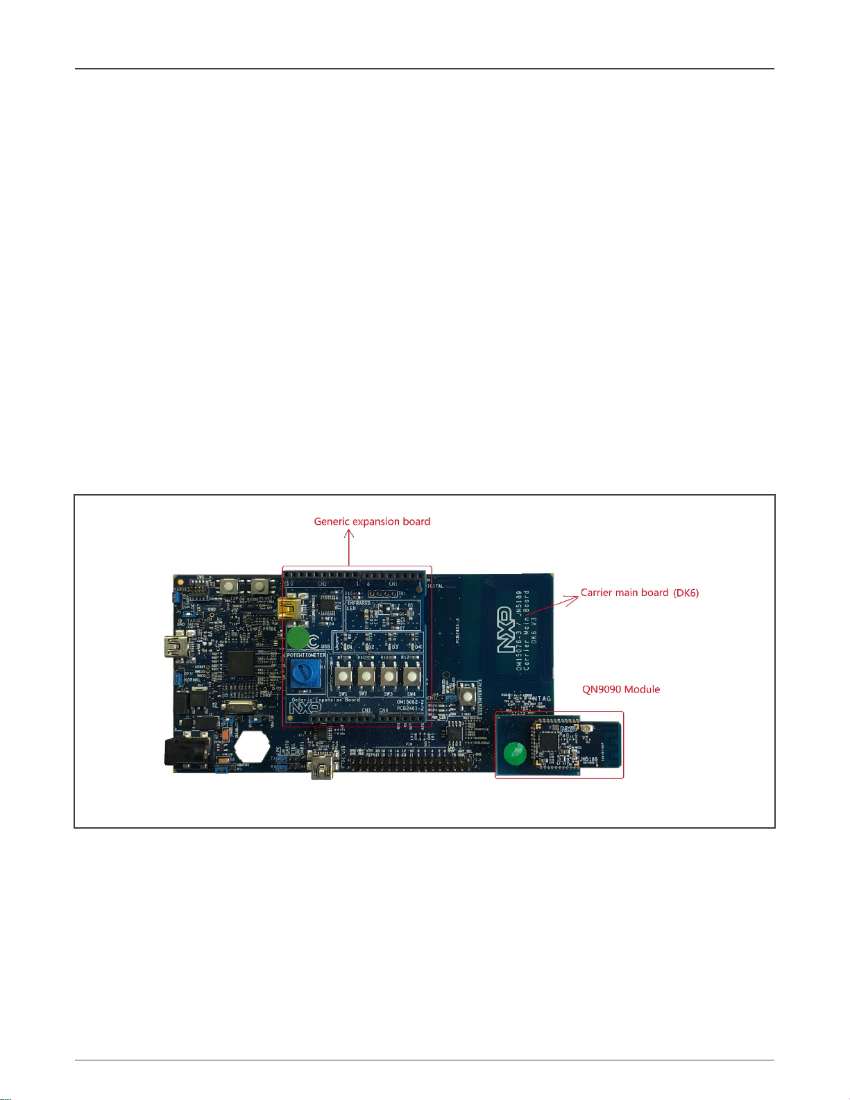
1.2 Kit contents
JN5189 DK includes the following boards:
• Carrier Main Board
• JN5189 Module board
• USB Dongle
• Generic expansion board
• Lighting Expansion board
Figure 1. Board overview
UM11368, Rev. 2, 11/2020
User's Guide 3 / 22
Page 4
NXP Semiconductors
Chapter 2
Carrier Main Board
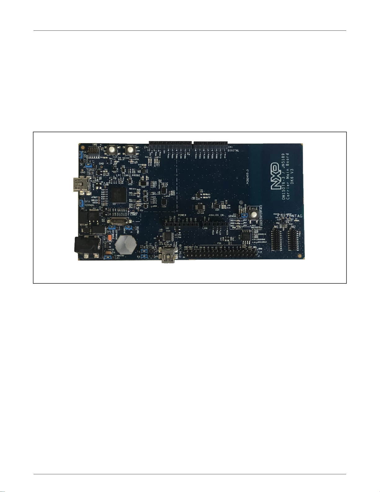
The OM15076 also called DK6 JN5189 carrier board provides a flexible development system for NXP’s JN5189 ultra-low
power, high performance wireless microcontroller. It can be used with a wide range of development tools, including NXP’s
MCUXpresso IDE. It has been developed by NXP to enable evaluation and prototyping with the JN5189_30_T Bluetooth Low
Energy wireless microcontroller.
The carrier boards (part number: OM15076) supplied in the development kit are physically identical. They are all pre-fitted with
an Arduino-compatible expansion board and a JN5189-based module with integrated antenna.
Figure 2. Carrier Main Board
2.1 Feature summary
The JN5189 Carrier board includes the following features:
• JN5189 module site
• NFC Tag with printed antenna
• On-board, high-speed USB based, Link2 debug probe with ARM’s CMSIS-DAP and SEGGER J-Link protocol options.
• Link2 probe can be used with on-board JN5189 or external target.
• Support for external debug probes.
• Power, Reset, ISP and UART Tx/Rx LEDs.
• Target Reset, and User buttons.
• Expansion options based on Arduino R3, plus additional expansion port pins.
• On-board 3.3V from USB port, 4xAAA batteries, 2xAAA batteries (low-power mode) or external power supply options.
• Built-in power consumption measurement.
• UART, I2C and SPI port bridging from LPC4233 target to USB via the on-board debug probe.
• 8Mb Macronix MX25R QSPI flash.
• FTDI USB connector.
UM11368, Rev. 2, 11/2020
User's Guide 4 / 22
Page 5
NXP Semiconductors
Carrier Main Board
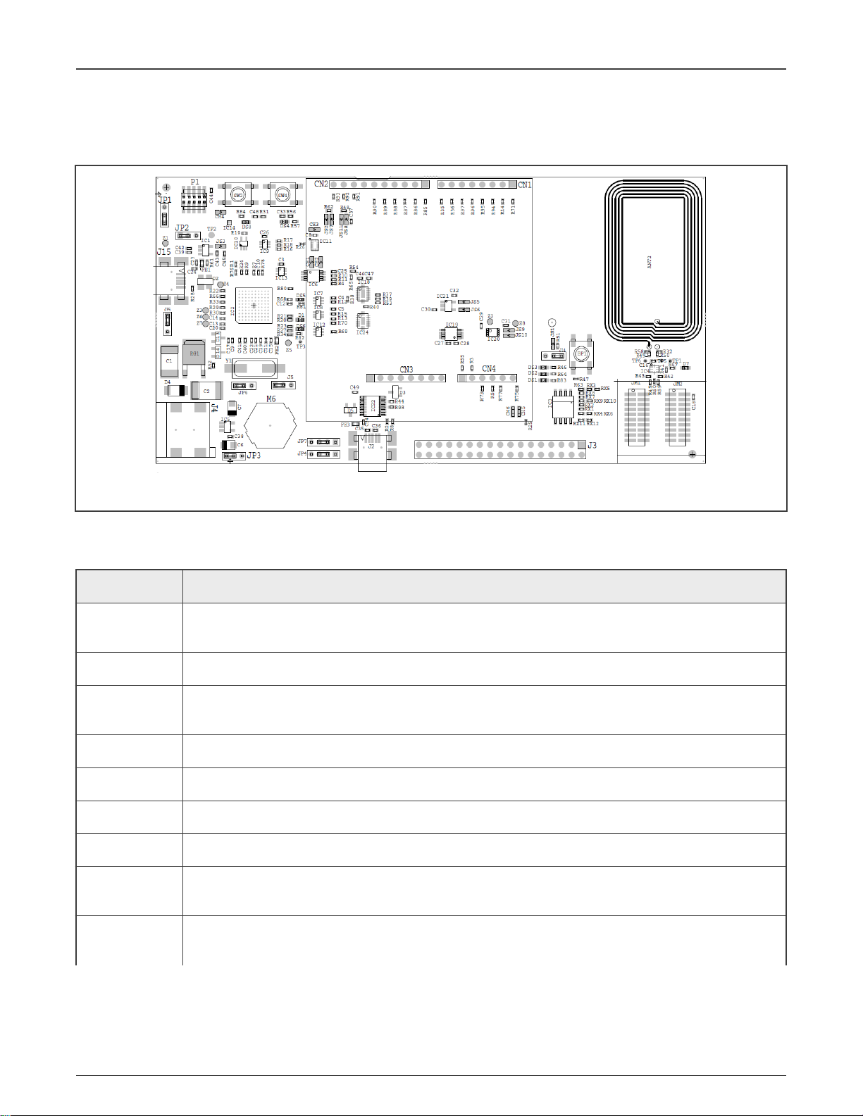
2.2 Board layout and settings
This section provides a quick reference guide to the main board components, configurable items, visual indicators and expansion
connectors. The layout of the components on the JN5189 Carrier board is shown in Figure 3.
Figure 3. Carrier board layout
The function of each identified component is listed in Table 1
Table 1. Table Board interface components
Circuit ref Description
D1 Link2 LPC4322 BOOT0_LED indicator. Reflects the state of LPC43xx Link2 MCU P1_1. When the boot
process fails, D1 will toggle at a 1 Hz rate for 60 seconds. After 60 seconds, the LPC4322 is reset.
DS1 JN5189 Power LED
DS2, DS3 2x Red debug LEDs connected respectively to JN5189 PIO_0 (DS2) and PIO_3 (DS3). LEDs are on anytime
the PIO is low.
DS4 JN5189 Reset LED – LED is on anytime the Target RESET is pulled low.
DS5, DS6 Green LEDs connected respectively to UART0_Tx (DS5) and UART0_Rx (DS6).
DS8 In System Programming (ISP) LED indicator. LED is ON when SW2 button is pressed.
IC2 Link2 MCU
J2 FTDI serial header. In addition to provide a serial output from JN5189, the Target side of the board can be
powered from the FTDI header. The JN5189 supports serial ISP boot from the FTDI header.
J3 32 pins Expansion header connector for debug. All the JN5189 IOs from modules and more are
available here.
Table continues on the next page...
UM11368, Rev. 2, 11/2020
User's Guide 5 / 22
Page 6
NXP Semiconductors
Carrier Main Board
Table 1. Table Board interface components (continued)
Circuit ref Description
J14 JN5189 VBAT current monitor V sense measurement. The V sense can be measured with a volt meter. Pin 1
(square pad) is positive and pin 2 is negative. JN5189 current is calculated by dividing the measured voltage
at J14 by the V sense resistance value of 3.3Ω.
J15 Link2 mini USB B-type connector. Powers both the Link2 side of the board and depending on the JP3, JP5
configuration, the JN5189 Target side of the board. Power the board from this connector when using the
on-board debug probe to debug the JN5189 Target MCU.
JP1 JN5189 Target SWD disable – 2-position jumper pins.
1. Jumper “ON” (default) the JN5189 Target SWD interface enabled. Normal operating mode where
the Target SWD is connected to either the on-board
2. Link2 debug probe or an external debug probe. Jumper “OFF”, the JN5189 Target SWD interface
is disabled. Use this setting only when the on-board Link2 debug probe is used to debug an
off-board Target JN5189.
JP2 SWD interface buffer power selection
JP3 JN5189 power source selection
1. Jumper fitted in position pin 1 - 2 (default -5V REG). Power source is either 5V from mini USB
connector or FTDI connector, or 4.5V from 3xAAA batteries or 5V from a 7-12V DC power supply
connected on J4.
2. Jumper fitted in position pin 2 - 3 (BAT 6V). Power source is 4xAAA batteries.
See details on Board power diagram Figure 5
JP4 Jumper to route LPC or FTDI to UART RX0 JN5189 (to change in pair with JP7)
JP5 Link2 (LPC4322) force DFU boot – 2 position jumper pins.
1. Jumper open (default) or shunted to boot mode for Link2 to follow the normal boot sequence. The
Link2 will boot from internal flash if image is found there. With the internal flash erased the Link2
normal boot sequence will fall through to DFU boot.
2. Jumper shunted to force the Link2 to DFU boot mode. Use this setting to reprogram the Link2
internal flash with a new image or to use the MCUXpresso IDE with CMSIS-DAP protocol.
JP6 JP6 is used to isolate the Link2 debug probe (SPI bridge function) from the JN5189 target to prevent leakage
current in power critical applications / current consumption analysis. JP6 needs to be fitted in position 1 - 2
to use the SPI bridging function between the JN5189 and Link2. This jumper is not fitted by default
JP7 Jumper to shunt LPC to JN5189 or FTDI to UART TX0 JN5189 (to change in pair with JP4)
CN1, CN2, CN3,
Expansion connectors, including Arduino Uno rev3 compatible connectivity.
CN4
JM1, JM2 JN5189 module headers
Table continues on the next page...
UM11368, Rev. 2, 11/2020
User's Guide 6 / 22
Page 7
NXP Semiconductors
Carrier Main Board
Table 1. Table Board interface components (continued)
Circuit ref Description
P1 10-pin SWD connector – The SWD connector is used to debug the JN5189 Target from an external debug
probe. The same SWD connector can also be used to connect the on-board Link2 debug probe to an
off-board target MCU (for this JP1 must be shunted).
BP1 User Interface button connected to IO1. Used in some Applications Notes.
SW2 In System Programming (ISP) button. JN5189 will enter ISP mode when SW2 is pressed during
hardware reset.
SW4 JN5189 Reset pushbutton.
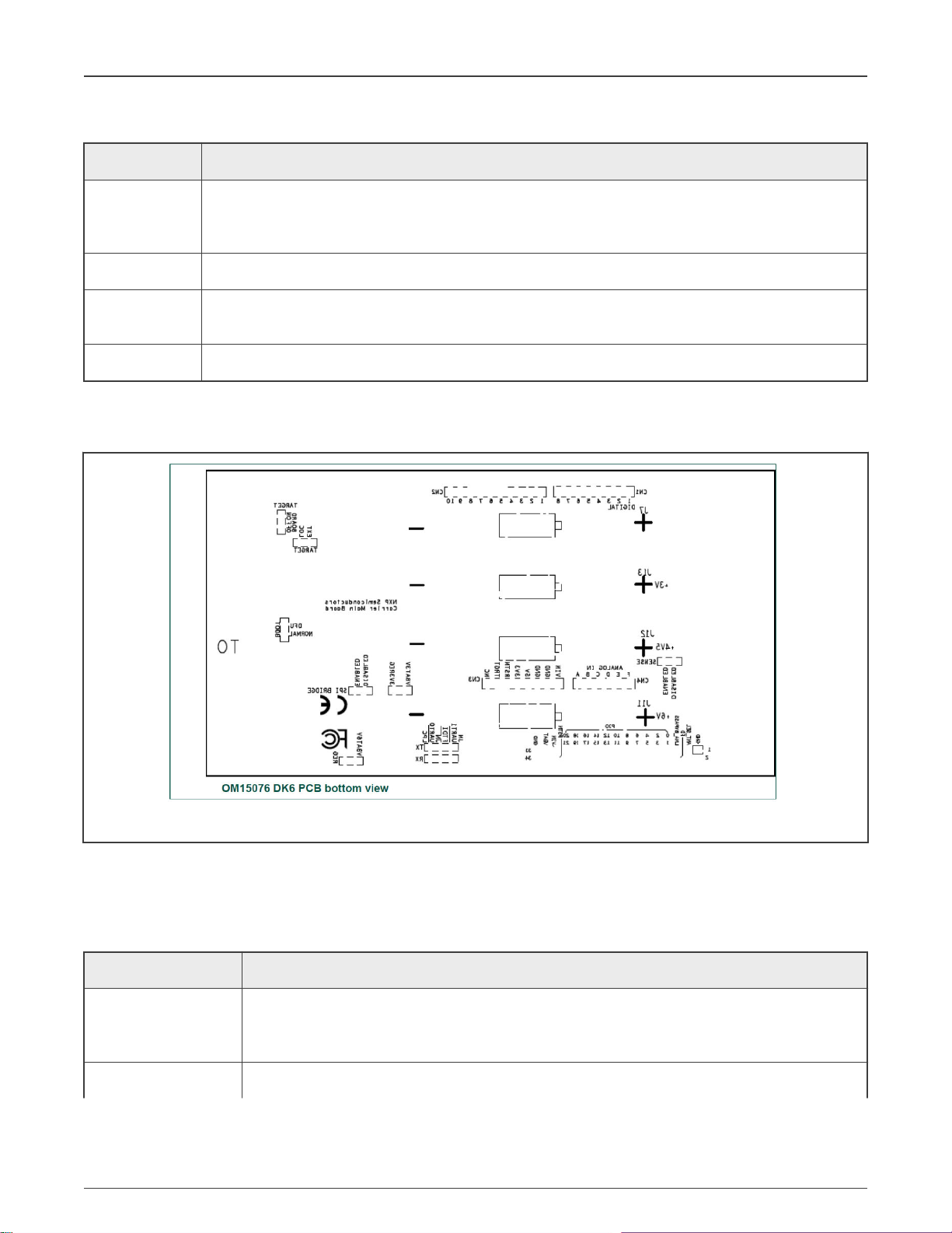
To ease the board usage and any debug the connectors serigraphy is also copied on PCB bottom.
J7, J13, J12 & J11 battery slots are also here.
Figure 4. OM15076 DK6 PCB bottom view
2.3 LED indicators
The DK6 board LED location are shown in Figure 3. A description of each on-board LED indicator is shown in next table
Table 2. LED indicator functions
LED reference Description
D1 Link2 MCU BOOT0_LED indicator. Reflects the state of Link2 MCU P1_1. When the boot process
fails, D1 will toggle at a 1 Hz rate for 60 seconds. After 60 seconds, the Link2 MCU is reset. It will be
ON when the Link2 MCU is Booting using DFU (See description for JP5).
DS1 JN5189 Power LED. This LED is on any time power is applied to the JN5189 wireless MCU.
Table continues on the next page...
UM11368, Rev. 2, 11/2020
User's Guide 7 / 22
Page 8

NXP Semiconductors
Carrier Main Board
Table 2. LED indicator functions (continued)
LED reference Description
DS2, DS3 2x Red debug LEDs connected respectively to JN5189 PIO_0 (DS2) and PIO_3 (DS3). LEDs are on
anytime the respective PIOs from the JN5189 are pulled low.
DS4 JN5189 Reset LED – LED is on anytime the Target RESET is pulled low.
DS5, DS6 2x Green LEDs connected respectively to UART0_Tx (DS5) and UART0_Rx (DS6). LEDs will flash
any time there is activity on the UART0.
DS8 In System Programming (ISP) LED indicator. LED is ON when IO5_ISP is pulled low and when SW2
button is pressed.
2.4 ARDUINO connectors
ARDUINO compatible connectors are based on Arduino R3.
References on the DK6 board are CN1, CN2, CN3, CN4.
The Generic expansion board OM15082 can be plugged into these connectors.
2.5 Buttons
2.5.1 Reset button
This button (SW4) is used to reset the JN5189 (note that the Link2 is NOT reset by this button)
2.5.2 ISP button
This button connects the JN5189_PIO5 (ISP_Entry) pin to ground. This should be used to set the JN5189 in ISP mode to program
a binary file into the chip memory.
To force entry into this ISP mode, hold down the ISP button (SW2), press and release the Reset button (SW4), then release the
ISP button (SW2). This is done automatically when using the DK6 Production Flash programmer with J2 (FTDI USB interface)
2.6 User Interface button
This button (BP1) is connected to JN5189_PIO_1 and should be used as an input
2.7 JN5189 Serial port
The JN5189 UART0 can also be connected through a virtual communication port (VCOM) UART bridge Link2 function either to
a host computer connected to the J2 USB FTDI or to J15 USB Link2. By default, the DK 6 is configured to use the FTDI USB.
For Link2 USB: The factory default CMSIS-DAP Link2 image includes UART bridge functionality (VCOM support), and
this firmware is also available with the LPCScrypt utility, available at https://www.nxp.com/design/microcontrollers-developer-
resources/lpc-microcontroller-utilities:LPC-UTILITIES power connections and measurements.
For the USB FTDI, the PC driver is available on FTDI website (the FTDI chip is already configured before the carrier board release).
2.8 Board power connections
A block diagram of the board power tree is shown in Figure 5. When the JN5189 Target is to be debugged from the on board Link2
probe, the USB mini B-type connector (J15) must connected to a Host computer. When the JN5189 Target is to be debugged from
an external debug probe, instead of the on-board debug probe, the Link USB connector (J15) must be disconnected.
UM11368, Rev. 2, 11/2020
User's Guide 8 / 22
Page 9

NXP Semiconductors
Figure 5. Board power diagram
The JN5189 Target VBAT selection is made at JP3, J5, with 3.3V from on-board LDO set as the default.
Carrier Main Board
2.9 Debug Configurations
The DK6 board has a built-in debug probe referred to as “Link2”. The JN5189 target wireless MCU can be debugged by the Link2
debugging probe, or from an external debug probe installed at P1. On-board jumpers JP1 and JP2 must be correctly positioned for
each mode. The on-board Link2 debug probe is capable of debugging target MCU’s with a VDDIO range of 1.6V to 3.6V. Check
the sections below for the appropriate jumper settings and how to properly power the board.
2.9.1 Debug using on-board debug probe
To use the on-board Link debug probe:
• The jumper JP2 must be fitted in position pin 1 - 2 (Local Target).
• Jumper JP1 must be open or fitted in position 2 – 3 to enable the target JN5189.
• Connecting the mini USB J15 to a host computer will power the Link and according JP3, JP5 position, the JN5189
sections of the board and provide the USB link to the debug tool software.
2.9.2 Debug using external debug probe
To use an external debug probe:
• connect the probe to the SWD (P1) connector
• power the JN5189 Target section of the board from the FTDI header (J1) or the Jack connector (J4)
• and fit a jumper to JP2 across pin 1 - 2 (Local Target).
• Jumper JP1 must be open or fitted across pin 2 – 3 to enable the target JN5189.
• The on-board Link2 debug probe must be unpowered, by leaving USB mini (J15) unconnected.
2.9.3 On-Board Link2 flash programming
To program the Link2 Flash the Link2 MCU must be in DFU mode. If the Link2 already has a valid image in the flash, you will
need to force it into DFU mode by placing a jumper shunt on JP5 across pin 1 - 2, then power the board by connecting the mini
USB J15 to a host computer. Link2 MCU programming is performed using the LPCScrypt utility (see https://www.nxp.com/design/
microcontrollers-developer-resources/lpc-microcontroller-utilities:LPC-UTILITIES). Instructions for using the tool are located at
the same web page.
UM11368, Rev. 2, 11/2020
User's Guide 9 / 22
Page 10

NXP Semiconductors
Carrier Main Board
2.9.4 Using the DK6 to debug an off-board target
The DK6 board’s Link2 debug probe may be used to debug an off-board target MCU. The on-board Link2 debug probe is capable
of debugging target MCU’s with a VDDIO range of 1.6V to 3.6V. To keep the on-board target JN5189 MCU from interfering with
the SWD interface:
• JP1 must be fitted across pin 1 - 2.
• The Link2 debug probe SWD is connected by a ribbon cable between the P1 connector to the off-board target MCU SWD
interface.
• Power the DK6 board from the Link USB connector J15,
• Fit jumper JP2 across pins 2 - 3 (External Target).
UM11368, Rev. 2, 11/2020
User's Guide 10 / 22
Page 11

NXP Semiconductors
Chapter 3
JN5189 Modules
JN5189 Module board is the JN5189 minimum system board. The module should be mounted to carrier board as the target. There
is a RF connector on this board, which can be used to RF signal testing.
Figure 6. JN5189 module board
UM11368, Rev. 2, 11/2020
User's Guide 11 / 22
Page 12

NXP Semiconductors
Chapter 4
Generic expansion board
This expansion board is available in the development kit and is compatible with Arduino shields. They are supplied pre-fitted with
Arduino-compatible header of Carrier Boards in the development kit.
The Generic Expansion Board has the following features:
• Arduino-compatible expansion header (in four parts, CN1-CN4)
• 4 user-input buttons (SW1, SW2, SW3, SW4) connected to DIOs on the JN5189 module on the Carrier Board:
— SW1 is connected to IO19
— SW2 is connected to IO15
— SW3 is connected to IO7
— SW4 is connected to IO4
• 4 LEDs (D1, D2, D3, D4) connected to DIOs on the JN5189 module on the Carrier Board:
— D1 is connected to IO16
— D2 is connected to IO6 (same as for the PWM output used on the Lighting/Sensor Expansion Board to drive the
three white LEDs)
— D3 is connected to IO3
— D4 is an optional LED which is not fitted on the supplied board and shares IO4 with button SW1
• Potentiometer connected to JN5189 ADC0, with a 0-1.8V DC voltage swing
• Infrared Emitting LED Vishay VSMB2948SL connected to JN5189 IO20_IR_Blaster
• USB Mini B port to provide access to JN5189 UART1 via IO11 and IO10 of JN5189 module (connected via FTDI FT230X
driver device)
• PCB pads for 4-way GPIO header (3V3, VCC, IO11, IO10), where IO11 and IO10 can be used to access JN5189 UART1
(in this case, the FTDI driver chip for the USB port must be isolated by removing resistors R9 and R16).
UM11368, Rev. 2, 11/2020
User's Guide 12 / 22
Page 13

NXP Semiconductors
Figure 7. Generic expansion board
Generic expansion board
UM11368, Rev. 2, 11/2020
User's Guide 13 / 22
Page 14

NXP Semiconductors
Chapter 5
Light expansion board
This expansion board is available in the development kit and is compatible with Arduino shields. They are supplied pre-fitted with
Arduino-compatible header of Carrier Boards in the development kit.
The Generic Expansion Board has the following features:
• Arduino-compatible expansion header (in four parts, CN1-CN4)
• 3 White LEDs (D1, D2, D3) connected to IO6 on the JN5189 module on the Carrier Board:
— D4 is an optional LED which is not fitted on the supplied board and shares IO4 with button SW1
• RGB LED controlled by I2C
• 2 Digital Microphones connected to DMIC interface in the JN5189
• 1 Temperature Sensor (IC8) connected by I2C
• 1 gyroscope (IC6) connected by I2C
• 1 Light Sensor (G1) connected by I2C
• 1 Accelerometer & Magnetometer (IC9) connected by I2C
Figure 8. Lighting expansion board
UM11368, Rev. 2, 11/2020
User's Guide 14 / 22
Page 15

NXP Semiconductors
Chapter 6
JN5189 USB Dongle
The OM15080-JN5189 can be used as a node in a Zigbee as a Zigbee Control Bridge, Zigbee Coordinator or packet sniffer. It can
also be used in Thread wireless network, typically dongle for Border Router, Network/Radio Co-Processor (NCP/RCP).
Figure 9. JN5189 USB Dongle
UM11368, Rev. 2, 11/2020
User's Guide 15 / 22
Page 16

NXP Semiconductors
Chapter 7
JN5189 current measurement
The JN5189 current can be measured:
1. Using the on-board current measurement circuit with MCUXpresso.
2. Measuring the voltage across a sense resistor (R51) in series with the supply,
3. A current meter on a modified DK6 board or a stand-alone module,
Each of these methods will be described in subsections below. When a board is attached, attempting to measure the lowest
possible power, the JN5189 IO pins must be configured by software configuration to avoid any extra current from the JN5189 IO
ports that have external pull-up or pull-down resistors enabled. JP6 should be opened to avoid leakage to the Link2 via the I2C
and SPI connections between it and the JN5189.
7.1 Current measurement with MCUXpresso
The DK6 board has an on-board current measurement circuit consisting of a MAX9634T (IC21) current monitor chip and a 12-bit
ADC (ADC122S021, IC19) with a 12-bit sample at 50k to 200ksps. The on-board MAX9634T current monitor measures the
voltage across the JN5189 VBAT Vsense resistor of 3.3Ω. The MAX9634 multiplies the sense voltage by 25 to provide a voltage
range suitable for the ADC to measure. The current measurement circuit is controlled by the debug processor and is not user
programmable. Power measurement utilities to use this feature are available in the MCUXpresso IDE installation.
Due to input offset voltage variations in the MAX9634, the current measurement circuit is not recommended for measuring current
below 150uA.
7.2 Vsense resistor measurement
The voltage across a series 3.3Ω resistor with the target JN5189 VBAT can be manually measured at J14 on the PCB. The
voltmeter positive probe is applied to J14 pin 1 (square pad) and negative probe to J14 pin 2. Use Ohm’s law to calculate the
current (JN5189 current = measured voltage / 3.3Ω). As an example, if the measured voltage is 10mV, then 10e-3 / 3.3Ω =
3.03mA. Note that the input current to the MAX9634 used in the on-board current measurement will be included in the voltage
measured across this resistor.
7.3 Current measurement with a multimeter
Figure 10 is the circuit for the power supply to the module. The signal VBAT is used to power the JN5189 module
UM11368, Rev. 2, 11/2020
User's Guide 16 / 22
Page 17

NXP Semiconductors
JN5189 current measurement
Figure 10. Power Sensing Circuit
This signal goes to the module (JM1.17) and the expansion connector (J3.31)
Figure 11. VBAT Connections
To measure the current using multimeter, remove R51 and place the multimeter across J14 pins 1 and 2.
UM11368, Rev. 2, 11/2020
User's Guide 17 / 22
Page 18

NXP Semiconductors
JN5189 current measurement
Figure 12. R51 Location
The multimeter will also measure the current take by the VSENSE line. This signal is used the measure the voltage drop across
the 3R3 resistor so that the current consumption results can be shown from with MCUXpresso. The current taken from this signal
is negligible but can be removed by cutting JS6.
Figure 13. Voltage Sense Circuit
7.4 IO Considerations
If an expansion board is not fitted then the following IO lines are connected on the DK6 board. Setting IOs incorrectly in the
software will cause current to be consumed and this should be taken into consideration when measurement current. The following
IOs are connected.
UM11368, Rev. 2, 11/2020
User's Guide 18 / 22
Page 19

NXP Semiconductors
Table 3. Connected IOs
JN5189 current measurement
Function PIOs Affected Schematic
Comment
Page number
NTAG 10, 11 4 Not connected by default. R45 and R59 are not fitted
by default
User Interface Button 1 4 Leave signal high and do not press switch
DS2 LED 0 4 Leave signal high
DS3 LED 3 4 Leave signal high
QSPI 16, 17, 18, 19,
20, 21
4 Negligible affect if QSPI is not used. To completely remove
any current consumption either remove IC3 or remove
RX1, 3, 4, 7, 9 and RX11 to disconnect all PIOs
Bridge SPI 0, 1, 2, 3, 7 7 Negligible effect. Remove IC18 and IC24
UART 8,9 (UART 0)
7 Remove jumpers on JP4 and JP7
0,1 (UART 1)
IC2 interface to LPC 10, 11 5 Disabled by default. No current draw if DIOS 10 and 11 are
high. Cut JS2 and JS11 to remove completely
Debug Interface 12, 13, 14 6 Negligible effect. Cut CH4 to disconnect
RESET and ISP buttons 5, RST 7 Negligible current drawn if not pressed. See Table for
Sleep current measurement
For sleep current measurements, the following additional changes are required to achieve the datasheet value otherwise the result
is typically 600nA high.
Table 4. Additional changes
Component Action Schematic Page Comment
R51 Remove 2 Allow connection of a Multimeter across J14
IC22 Remove
7 See Section 5.5 below
3V3OUT
D5 Remove 7 Disconnect ISPEN from FTDI device
C33 Remove 7 Remove capacitor from Reset Line
R64 Remove 7 Remove Pullup Resistor from ISPEN
IC21 or cut JS5-6 Remove 6 Disconnect current sense amplifier
IC11 Remove 6 Disconnect control lines from LPC debug interface
UM11368, Rev. 2, 11/2020
User's Guide 19 / 22
Page 20

NXP Semiconductors
JN5189 current measurement
7.5 Running the DK6 board at different voltages
In order to run the DK6 at different voltages, it is necessary to disconnect the FTDI 3V3OUT signal otherwise this will continue to
supply 3.3V to the board. The circuit is shown below in Figure 14
Figure 14. FTDI Interface
It is important to leave C49 connected to Pin10 of the FT230A. To achieve this modify the boards as shown in Figure 15.
Figure 15. 3V3OUT modification
UM11368, Rev. 2, 11/2020
User's Guide 20 / 22
Page 21

NXP Semiconductors
Chapter 8
Revision history
Table 5. Revision history
Rev Date Description
0 20200115 Initial release
1 20200428 Added Lighting Expansion and USB Dongle
2 20201102 Update
UM11368, Rev. 2, 11/2020
User's Guide 21 / 22
Page 22

How To Reach Us
Home Page:
nxp.com
Web Support:
nxp.com/support
Information in this document is provided solely to enable system and software implementers
to use NXP products. There are no express or implied copyright licenses granted hereunder
to design or fabricate any integrated circuits based on the information in this document. NXP
reserves the right to make changes without further notice to any products herein.
NXP makes no warranty, representation, or guarantee regarding the suitability of its products
for any particular purpose, nor does NXP assume any liability arising out of the application
or use of any product or circuit, and specifically disclaims any and all liability, including
without limitation consequential or incidental damages. “Typical” parameters that may be
provided in NXP data sheets and/or specifications can and do vary in different applications,
and actual performance may vary over time. All operating parameters, including “typicals,”
must be validated for each customer application by customer's technical experts. NXP does
not convey any license under its patent rights nor the rights of others. NXP sells products
pursuant to standard terms and conditions of sale, which can be found at the following address:
nxp.com/SalesTermsandConditions.
Security — Customer understands that all NXP products may be subject to unidentified
or documented vulnerabilities. Customer is responsible for the design and operation of its
applications and products throughout their lifecycles to reduce the effect of these vulnerabilities
on customer’s applications and products. Customer’s responsibility also extends to other open
and/or proprietary technologies supported by NXP products for use in customer’s applications.
NXP accepts no liability for any vulnerability. Customer should regularly check security updates
from NXP and follow up appropriately. Customer shall select products with security features
that best meet rules, regulations, and standards of the intended application and make the
ultimate design decisions regarding its products and is solely responsible for compliance with
all legal, regulatory, and security related requirements concerning its products, regardless of
any information or support that may be provided by NXP. NXP has a Product Security Incident
Response Team (PSIRT) (reachable at PSIRT@nxp.com) that manages the investigation,
reporting, and solution release to security vulnerabilities of NXP products.
NXP, the NXP logo, and NXP SECURE CONNECTIONS FOR A SMARTER WORLD are
trademarks of NXP B.V. All other product or service names are the property of their respective
owners. AMBA, Arm, Arm7, Arm7TDMI, Arm9, Arm11, Artisan, big.LITTLE, Cordio, CoreLink,
CoreSight, Cortex, DesignStart, DynamIQ, Jazelle, Keil, Mali, Mbed, Mbed Enabled, NEON,
POP, RealView, SecurCore, Socrates, Thumb, TrustZone, ULINK, ULINK2, ULINK-ME, ULINK-
PLUS, ULINKpro, µVision, Versatile are trademarks or registered trademarks of Arm Limited (or
its subsidiaries) in the US and/or elsewhere. The related technology may be protected by any
or all of patents, copyrights, designs and trade secrets. All rights reserved. Oracle and Java are
registered trademarks of Oracle and/or its affiliates. The Power Architecture and Power.org word
marks and the Power and Power.org logos and related marks are trademarks and service marks
licensed by Power.org.
©
NXP B.V. 2020. All rights reserved.
For more information, please visit: http://www.nxp.com
For sales office addresses, please send an email to: salesaddresses@nxp.com
Date of release: 11/2020
Document identifier: UM11368
 Loading...