

Page 1

UM11227
NTM88 family of tire pressure monitor sensors
Rev. 7 — 29 March 2021 User manual
Document information
Information Content
Keywords NTM88, features, architecture, programming model, 8-bit microcontroller
(MCU), pressure sensor, accelerometer, programmable RF transmitter and
flexible LF receiver
Abstract This user manual describes the features, architecture, and programming
model of the NTM88 family of devices.
Page 2

NXP Semiconductors
UM11227
NTM88 family of tire pressure monitor sensors
Revision history
Document ID Release
date
UM11227 v.7 20210329 • Global changes as follows:
UM11227 v.6 20200424 • Section 3, revised second bullet for "Optional accelerometer ranges" and added a footnote.
Description
– Performed minor grammatical, content and tyopgraphic revisions throughout.
– Revised "SRS" to "SIMRS" in six locations.
• Inserted new document information table on the first page of the data sheet.
• Section 1, relocated the revision history to the front of the document to comply with NXP
content guidelines for user manuals.
• Section 3, revised as follows:
– Revised "Pressure range: 90 kPa to 930 kPa" to "Optional pressure ranges".
– Removed "Optional accelerometer range: See Section 4."
– Revised "Slave SPI to support..." to "Client SPI to support..."
• Section 4, Table 1, revised the "Type number" from "NTM88Hxx5" to "NTM88Hxxx" and
"NTM88Jxxx".
• Section 4.5, revised "At address $FC00, 1024 bytes..." to "At address $FC00, 512 bytes..."
• Section 5.1 revised as follows:
– Step 1: revised the content.
– Table 3: revised the part number from "NTM88H05xT1" to "NTM88xxxxT1", the pressure
value from "H" to "y" and updated footnote 3.
• Section 9.1, revised the first paragraph adding a statement to visit the NXP website for
user guides, application notes and evaluation hardware collateral.
• Section 10.19.1.3, Figure 47, revised the title.
• Section 10.19.2.4, revised the note below Table 155.
• Section 11, Figure 60, revised the title.
• Section 5.1, revised as follows:
– Table 3, revised tables notes 1, 3, 4, and 5.
– Table 4, revised table note 1
• Section 10.1.1, deleted rows for register map addresses $E7E0 through $E7FF.
• Section 10.2.2, deleted the last paragraph starting with "The LF, SMI, and ADU user...."
• Section 10.3, Table 17, revised vector priority 8 removing "reserved" and providing values.
• Section 10.12.1, revised as follows:
– Moved the figure titled "KBI block diagram" to Section 10.12.2.1 prior to Table 36.
– Moved the figure titled "External interrupt logic" to Section 10.12.2.4 prior to Table 42.
– Figure 14, revised image.
– Table 23, in the "Pull enable" row, revised the "x" in the "KBI pin enable" column to "0".
• Section 10.12.1.1, revised as follows:
– Removed second paragraph starting with "PTA[4:0] pins are shared with on-chip
peripheral functions."
– Removed redundant Figures titled "General purpose I/O block diagram" and "General
purpose I/O logic".
– Removed redundant Table titled "Truth table for pullup and pulldown resistors".
– Table 37, revised the "Description" for "KBACK".
• Section 10.12.2.4, Table 43, revised the "Description" for "IRQACK".
• Section 10.14.1.1, Table 63, revised the "Description" for "WUFACK" and "PRFACK".
• Section 10.15.17.5, Table 84, revised the "Description" for "LFIAK".
• Section 10.16.11.8, Table 118, revised the "Description" for "RFIAK".
• Section 10.19.2.1, Table 147, revised the "Description" for "SMIFAK".
• Section 10.19.2.3, Table 151, revised the description for 1:0, FILT[1:0]
UM11227 All information provided in this document is subject to legal disclaimers. © NXP B.V. 2021. All rights reserved.
User manual Rev. 7 — 29 March 2021
2 / 207
Page 3
NXP Semiconductors
UM11227
NTM88 family of tire pressure monitor sensors
Revision history...continued
Document ID Release
date
UM11227 v.5 20200124 • Section 10.19, revised entire section.
UM11227 v.4 20191004 • Section 3: Revised third bullet under "Transducer measurement interfaces" from "12-bit
UM11227 v.3 20190822 • Section 2, revised the general description paragraph.
Description
UM11227 v.6 (Continued)
• Section 10.23.3.1, Table 175, revised and unmerged the Bit 6 cell for "R" and "W", inserting
"0" in Bit 6 for "R" and revised the "Description" for "RTIACK" in Table 176.
• Section 10.23.3.2, Table 177, revised and unmerged the Bit 6 cell for "R" and "W", inserting
"0" in Bit 6 for "R" and revised the "Description" for "LVDACK" in Table 178.
• Section 10.23.3.3, Table 179, revised and unmerged the Bit 2 cell for "R" and "W", inserting
"0" in Bit 2 for "R" and revised the "Description" for "PPDACK" in Table 180.
• Section 10.25, inserted a new first bullet, revised the second bullet, and inserted a new
bullet before the last bullet.
• Section 10.26, Added new first paragraph.
• Section 10.26.6, revised the first sentence and the figure title for Figure 59.
• Section 11, revised the paragaph starting with "A gel is used to provide media protection...",
adding two new sentences at the end of the paragraph.
compensated..." to "8-bit compensated...."
• Section 4.1: Revised the first bullet adding "For devices programmed by NXP with an
embedded firmware..." and added new paragraph beginning with "Prototype samples...."
• Section 4.4, revised the second paragraph.
• Section 7.3, Figure 4: Revised Figure 4.
• Section 10.1.1, Table 15, revised rows $1860, $1861 and $FD66:$FDFA.
• Section 10.8.5.2, Table 20: Removed "Normal Temperature Restart" row.
• Section 10.8.5.4: Removed section titled "Temperature restart" that followed
Section 10.8.5.4.14.
• Section 10.9.1, Table 21, revised as follows:
– Start Address $FC00, revised the "End Address" from "$FD65" to "$FD3F" and updated
the "Block description".
– Start Address $FD40, revised "Start Address "from $FD66" to "$FD40" and updated the
"Block description".
– Start Address $FFC0, revised "End address" from "$FFDB" to "$FFDF" and updated the
"Block description".
– Start Address $FFDC, removed entire row.
• Section 10.16.11.1, Table 104: Added new table.
• Section 10.16.11.3, Table 108: Revised the description for "4:0, PWR[4:0]".
• Section 10.16.11.9, Table 123: Revised the description for "15:3, AFREQ[12:0]".
• Section 10.16.11.11: Revised "RFCR8" to "EPR" in three locations.
• Section 10.16.11.12: Revised "RFCR9" to "RFPRECHARGE" in three locations.
• Section 10.19.2.3, Table 151, added "Recommend adjusting to 500 Hz or higher when
either or both ISD[3:0] / SP[3:0] are configured for times < 1024 ms." to the description for
FILT[1:0] for the case of "0 0 = 250 Hz".
• Section 11, Figure 60: revised the image.
• Section 3, revised as follows:
– Revised the supporting bulleted items of the bullet "Transducer measurement interfaces
with low-power AFE."
– Revised "16k bytes flash memory" to "16 kB flash memory" below "8-bit S08 compact
instruction set controller."
• Section 4, Table 1: revised the description.
UM11227 All information provided in this document is subject to legal disclaimers. © NXP B.V. 2021. All rights reserved.
User manual Rev. 7 — 29 March 2021
3 / 207
Page 4
NXP Semiconductors
UM11227
NTM88 family of tire pressure monitor sensors
Revision history...continued
Document ID Release
date
UM11227 v.2 20190516 • The format of this document has been redesigned to comply with the identity guidelines of
NTM88RM v.1 20181214 • Initial release
Description
UM11227 v.3 Modifications (Continued.)
• Section 4.1, replaced table titled "CodeF - tolerance and firmware configuration encoding"
with a paragraph and bullets.
• Section 4.2, replaced table titled "CodeH - hardware configuration encoding" with a
paragraph and bullets.
• Section 4.3: revised as follows:
– Table 2, bits 7 through 0, removed table 2 reference for CODEF, removed table 3
reference for CODEH and replaced references with "Consult the appropriate NTM88
product data sheet for a description."
– Revised "ID27 — 0 to identify NTM88 family" to "ID27 — 1 to identify NTM88 family."
• Section 5.1, Table 3: Revised footnote 5.
• Section 6: revised the first paragraph.
• Section 6, Figure 2, revised the figure caption.
• Section 7, added introductory paragraph.
• Section 7.1: Revised the image in Figure 3.
• Section 7.2, Table 5: Revised the symbols for pins 1 through 6 from "NC" to "n.c." to
support changes made to the image in Figure 3.
• Section 10.1.1, Table 15, revised as follows
– Address $0008, revised all entries to "reserved."
– Address $1809, revised Bit1 to "reserved."
– Address $180C, revised Bit3, Bit2, and Bit0 to "reserved."
– Address $FDFF, revised Bit7 to "ID31," Bit6 to "ID30," Bit5 to "ID29," and Bit4 to "ID28."
• Removed the section titled "Port input filter enable register (PORTIFE)" that followed
Section 10.12.1.7.
• Section 10.16.9, Figure 38: revised the figure.
• Section 10.16.11.12, revised as follows:
– Table 128, revised "Reset ($00)" to "Reset ($40) and the "TIMEOUT0" bit from "0" to "1".
– Table 129, revised the description for 7:6.
• Section 10.19, Figure 44: revised the figure.
• Section 10.19.1: revised as follows:
– Revised the last sentence before Table 145.
– Table 145: Added "Stop4 entry not recommended." to the "Comments" for "Direct"
• Section 10.19.1.2: Revised 5th paragraph, 2nd sentence.
• Section 10.23.3.2, Table 177, removed "BGBDS" from Bit1
• Section 10.23.3.2, Table 178, removed "BGBDS" row from table.
• Section 10.23.3.4, Table 181, removed "HVWF" from Bit3, "HVWACK" from Bit2, and
"HVWE" from Bit 0.
• Section 10.23.3.4, Table 182, removed rows for "HVWF", "HVWACK," and "HVWE."
• Section 11: Added new paragraph before Figure 60.
NXP Semiconductors.
• Legal texts have been adapted to the new company name where appropriate.
• Revised document number from "NTM88RM" to "UM11227".
• UM11227 v.2 supercedes NTM88RM v.1.
UM11227 All information provided in this document is subject to legal disclaimers. © NXP B.V. 2021. All rights reserved.
User manual Rev. 7 — 29 March 2021
4 / 207
Page 5

NXP Semiconductors
1 Introduction
1.1 Purpose
This user manual describes the features, architecture, and programming model of the
NTM88 family of devices.
1.2 Audience
This document is primarily for system architects and software application developers who
are using or considering the use of the NTM88 in a system.
2 General description
The NTM88 is a small (4 mm x 4 mm x 1.98 mm), fully integrated tire pressure monitoring
sensor (TPMS). It also provides low transmitting power consumption, large customer
memory size, and a choice of either dual- or single-axis accelerometer architecture.
The NTM88 TPMS solution integrates an 8-bit microcontroller (MCU), pressure sensor,
accelerometer, and RF transmitter.
UM11227
NTM88 family of tire pressure monitor sensors
3 Features and benefits
• Optional pressure ranges
• Optional single- or dual-axis accelerometer ranges
• Transducer measurement interfaces with low-power AFE:
– 10-bit compensated pressure sense element
– 10-bit compensated accelerometers
– 8-bit compensated internal device temperature measurement
– 8-bit compensated internal device voltage measurement
– Two I/O pins can be used for external signals
• 8-bit S08 compact instruction set controller:
– 64 bytes low-power “always on“ NVM parameter registers
– 512 bytes SRAM
– 16 kB flash memory (512 bytes reserved for NXP coefficients)
– Family of NXP firmware libraries available via royalty-free license
• Programmable RF transmitter
– Characterized for RF carrier typical of 315 MHz or 434 MHz
– Characterized for FSK in ~3 kHz increments or OOK modulation
– Characterized for baud rate examples of 9.6 kbp/s, 19.2 kbp/s, and 38.4 kbp/s
• Flexible 125 kHz LF receiver:
– Capability for ASK or OOK demodulation
– Automated Manchester decoding
• Two channel timer / pulse-width module
• Client SPI to support host access to internal peripherals, registers, and memory
• Seven GPIOs with programmable multiplexing to support software development,
external ADC input, timer, SPI, and wake-up
• Qualified in compliance with AEC-Q100, Rev. H
1
1
1 Consult NXP sales for details or specific requests.
UM11227 All information provided in this document is subject to legal disclaimers. © NXP B.V. 2021. All rights reserved.
User manual Rev. 7 — 29 March 2021
5 / 207
Page 6

NXP Semiconductors
• Long battery service life
• Temperature sensor
• Voltage reference measured by ADC10
• Six-channel, 10-bit analog-to-digital converter (ADC10) with two external I/O inputs
• Internal 315-/434-M Hz RF transmitter
– External crystal oscillator
– PLL-based output with fractional-n divider
– OOK and FSK modulation capability
– Programmable data rate generator
– Manchester, Bi-Phase, or NRZ data encoding
– 256-bit RF data buffer variable length interrupt
– Direct access to RF transmitter from MCU for unique formats
– Low-power consumption
• Differential input LF detector/decoder on independent signal pins
• Real-time Interrupt driven by LFO with intervals of 2, 4, 8, 16, 32, 64, or 128 ms
• Free-running counter, low-power, wake up timer and periodic reset driven by LFO
• Watchdog timeout with selectable times and clock sources
• Two-channel general-purpose timer/PWM module (TPM1)
• Internal oscillators
– MCU bus clock of 0.5, 1, 2, and 4 MHz (1, 2, 4, and 8 MHz HFO)
– Low frequency, low-power time clock (LFO) with 1 ms period
– Medium frequency, controller clock (MFO) of 8 μs period
• Low-voltage detection
UM11227
NTM88 family of tire pressure monitor sensors
4 Configuration options
Table 1. Ordering information
PackageType number
Name Description Version
NTM88Hxxx
NTM88Jxxx
HQFN24 Plastic thermal enhanced quad flat package; no leads, 0.1 dimple wettable
flank; 24 terminals; 0.5 mm pitch, 4 mm x 4 mm x 1.98 mm body
4.1 Electronic encoding - "CodeF"
Consult the appropriate NTM88 product data sheet for a description of the CodeF
traceability which allows the user to extract:
• For devices programmed by NXP with an embedded firmware, configuration values
holding the firmware library used for final test
• Accelerometer variant type
Prototype samples may be configured and delivered with the firmware remaining in
the flash memory upon special request. The series production process will erase the
firmware from flash memory to facilitate customers choice of the firmware routines, while
excluding specific firmware routines the application software does not require. Consult
the appropriate NTM88 firmware user guide for a description of the available firmware
routines, either as firmware in flash, or as library releases.
SOT1931-1(D)
UM11227 All information provided in this document is subject to legal disclaimers. © NXP B.V. 2021. All rights reserved.
User manual Rev. 7 — 29 March 2021
6 / 207
Page 7

NXP Semiconductors
UM11227
NTM88 family of tire pressure monitor sensors
4.2 Electronic encoding - "CodeH"
Consult the appropriate NTM88 product data sheet for a description of the CodeH
traceability which allows users to extract:
• configuration values holding the assembly revision
• final test pressure
• accelerometer calibrations
4.3 Device identification
The bytes assigned to identify the device and its options are described below. This data
can be read using the TPMS_READ_ID routine.
Table 2. Device ID coding summary
ID Address
00 CODEF Consult the appropriate NTM88 product data sheet for a description.
01 CODEH Consult the appropriate NTM88 product data sheet for a description.
02 CODE2 ID7 ID6 ID5 ID4 ID3 ID2 ID1 ID0
03 CODE3 ID15 ID14 ID13 ID12 ID11 ID10 ID9 ID8
04 CODE4 ID23 ID22 ID21 ID20 ID19 ID18 ID17 ID16
05 CODE5 ID31 ID30 ID29 ID28 ID27 ID26 ID25 ID24
Register
Name
7 6 5 4 3 2 1 0
BIT
ID13:0 — Device ID within each assembly lot - 16k devices in each lot
ID26:14 — Lower 13 bits of assembly lot ID - 32k lots
ID27 — 1 to identify NTM88 family
ID28:29 — Upper 2 bits of assembly lot ID
ID30 — 0x1 to identify sub-con B, 0x0 to identify sub-con A
ID31 — 0x1 to identify NXP as device supplier
Note: Prior to erasing the flash memory, users are advised to first copy the contents of
the CODEF through CODE5 data into a secure and retrievable database when using, for
example, a custom gang programmer in lieu of the CodeWarrior IDE tool. The contents
of CODEF through CODE5 are unique to each part number, configuration of pressure
and accelerometer ranges, and serial numbers, and must be replaced as part of the user
flash programming processes.
4.4 Definition of signal ranges
Each measured parameter (pressure, voltage, temperature, acceleration) results from
an ADC10 conversion of an analog signal. This ADC10 result may then be passed
by the firmware to the application software as either the raw ADC10 result or further
compensated and scaled for an output between one and the maximum digital value
minus one. The minimum digital value of zero and the maximum digital value are
reserved as error codes.
The signal ranges and their significant data points are shown in Figure 1. In this
definition, the signal source would normally output a signal between S
UM11227 All information provided in this document is subject to legal disclaimers. © NXP B.V. 2021. All rights reserved.
User manual Rev. 7 — 29 March 2021
INLO
and S
INHI
. Due
7 / 207
Page 8
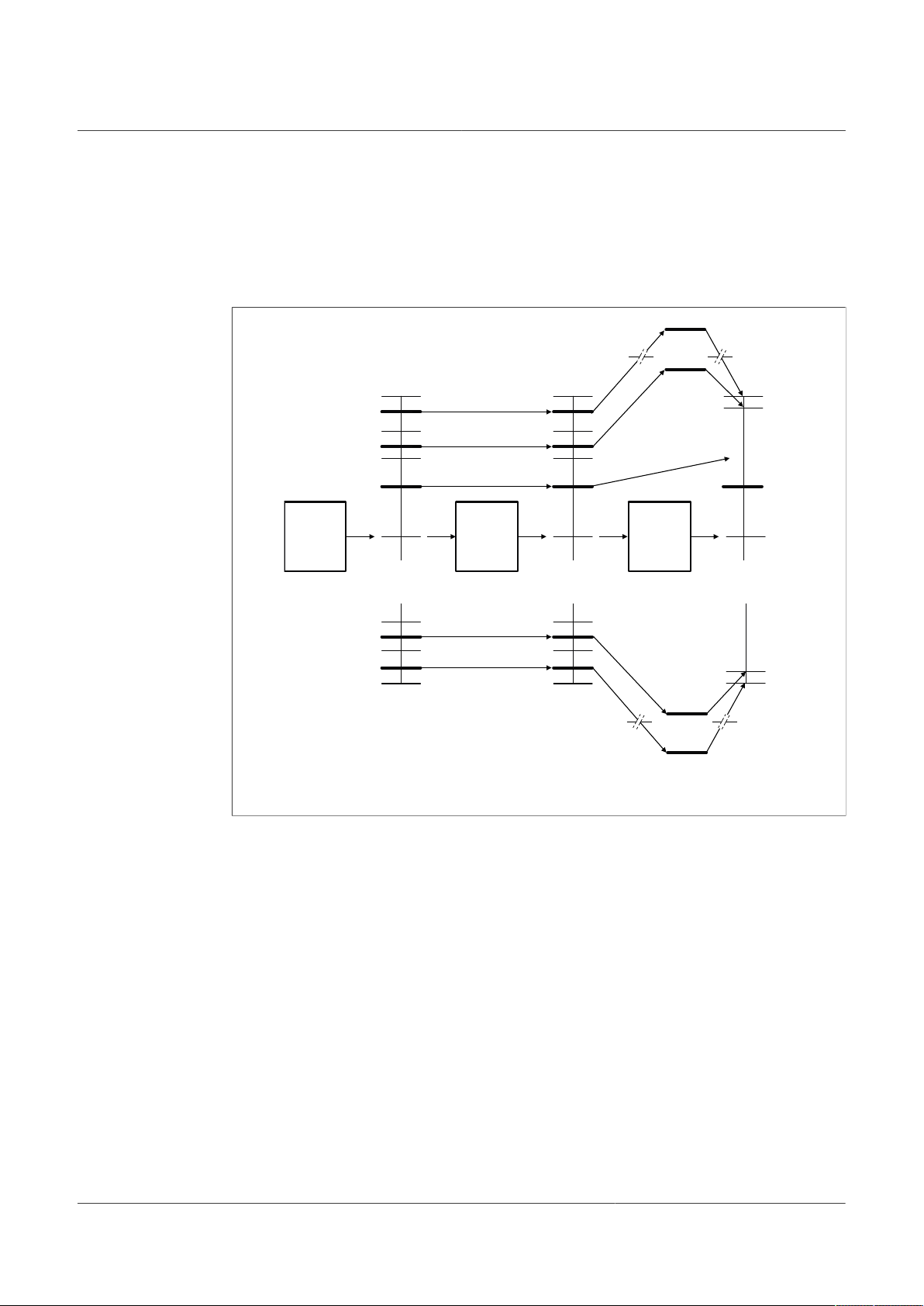
NXP Semiconductors
SENSOR
ANALOG
VOLTAGE
ADC10 RAW
DIGITAL
(10-BIT CONVERSION)
CALCULATED
DIGITAL
(9-BIT EXAMPLE)
SIGNAL
SOURCE
ADC10
FIRMWARE
ROUTINE
511
510
0
1
256
0
1023
512
VDD/2
VDD
VDD
SINMAX
SINHI
SINMIN
SINLO
DINMAX
DINHI
DINLO
DINMIN
NORMAL CASE
UNDERFLOW
LOWER ERROR CASE
CASE
OVERFLOW
CASE
FORCE
OUTPUT
TO 511
FORCE
OUTPUT
TO ZERO
UPPER ERROR CASE
aaa-028041
to process, temperature, and voltage variations, this signal may increase its range to
S
INMIN
the signal is between the supply rails, so that the ADC10 converts it to a range of digital
numbers between 0 and 1023. These digital numbers have corresponding D
D
INHI
and scaled to give the required output code range.
to S
, D
UM11227
NTM88 family of tire pressure monitor sensors
. In the example case of 10-bit raw conversions and 9-bit compensation,
INMAX
INMIN
values. The ADC10 digital value is taken by the firmware and compensated
INMAX
, D
INLO
,
Figure 1. Measurement signal range definitions
Digital input values below D
and above D
INMIN
are immediately flagged as being out
INMAX
of range and generate error bits and the output is forced to the 0 value.
and D
) or above D
INMIN
will normally produce an output between 1 to
INHI
(but not D
INHI
INMAX
) will most
Digital values below D
likely cause an output that would be less than 1 or greater than 510, respectively. These
cases are considered underflow or overflow, respectively. Underflow results will be forced
to a value of 1. Overflow results will be forced to a value of 510.
Digital values between D
510 (for a 9-bit result). In some isolated cases due to compensation calculations and
rounding, the result may be less than 1 or greater than 510, in which case the underflow
(but above D
INLO
INLO
and overflow rule mentioned above is used.
UM11227 All information provided in this document is subject to legal disclaimers. © NXP B.V. 2021. All rights reserved.
User manual Rev. 7 — 29 March 2021
4.5 Memory resource usage
At address $FC00, 512 bytes are protected from erasure, containing the sensitivity and
offset coefficients for the transducers and clocks.
The firmware uses no specific bytes of the RAM but will cause additional stacking of
temporary values.
8 / 207
Page 9

NXP Semiconductors
The firmware uses 2 bytes ($008E and $008F) of the Parameter Registers for global
flags for all routines.
5 Marking
5.1 Exterior markings
The marking2 on the NTM88 family contain three lines of text, described as follows:
1. Line 1 identifies the location of pin 1 and, when appropriate, shows the corporate logo
2. Line 2 identifies part marking information, see Table 3 for details on the NTM88
3. Line 3 is the trace code. See Table 4 for trace code definitions.
Table 3. Example Exterior Marking
Part Number Company
NTM88xxxxT1 N 8 y a a x
markings.
[1]
Family
UM11227
NTM88 family of tire pressure monitor sensors
Marking
[2]
Pressure
[3]
Accelerometer
[4]
Mechanical
[5]
[1] Company column: N = qualified.
[2] Family column: Always "8".
[3] Pressure column: Where "y" is a letter representing the pressure configuration.
[4] Accelerometer columns: Where "a a" are two letters representing the accelerometer configuration.
[5] Mechanical column: Where "x" is a letter representing the mechanical configuration.
Table 4. Trace code definitions
Trace code Definition
A Assembly site
[1]
L Wafer lot
YW Year and work week
Z Assembly lot split
[1] "X" for site #1; additional letters for other assembly sites as needed.
[2] “Z” can be up to two characters "ZZ" when the number of subassembly lots > 26
[2]
2 Subject to change by NXP without notice.
UM11227 All information provided in this document is subject to legal disclaimers. © NXP B.V. 2021. All rights reserved.
User manual Rev. 7 — 29 March 2021
9 / 207
Page 10
NXP Semiconductors
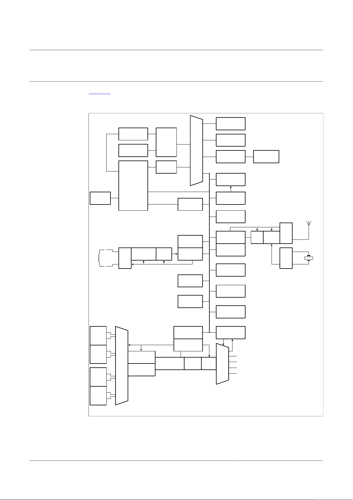
BDM
CONTROLLER
S08
8b CPU
M0
BUS
ARB.
MUX
A
TO D
MUX
C
TO V
MUX
S0
M1
INTERRUPT
CONTROLLER
SPIPADMUX
GPIO
IRQ
BKGD
SPI
TPM
ADC
ETC.
NV RAM
64 x 8
PWR. MODE
CONTROLLER
RESET
CNTL. MOD.
KEYBD
INTERRUPT
LF RX
REG. FILE
FREE
RUN CNTR .
peripheral bus
2chTPM
LF RX
SMI
LPFBUFFER
aaa- 031049
SYSTEM
INT. MOD.
RF TX
REG. FILE
TX PLL
DIGITAL
SUB
GHz
DE-
CODE
AZ, RECT.
GAIN, SLICE
TX
PA
125
kHz
AFE
P-CELL
SENSE
P-CELL
REF.
G-CELL
NORTH
G-CELL
SOUTH
off- chip 26 MHz
off-c hip LF coil
off-c hip antenna
SQ
OSC
RF TX
INT. CLKS
SYS
COP
TIMER
PWU/RTI
TIMER
GAIN, OFFSET
AND COEFF.
GAIN, OFFSET
AMPS
SAR
ADC
Offset
DAC
C TO V
CONVERTER
bandgap
temp sensor
ext. A2D V0
ext. A2D V1
S1
SYS RAM
512 x 8
S2
S3
FLASH
CONTROLLER
FLASH N VM
16 k x 8
PTA0 - 4
PTB0 - 1
6 Block diagram
Figure 2 presents the device's main blocks and their signal interactions. Power
management controls and bus control signals are not shown in this block diagram for
clarity.
UM11227
NTM88 family of tire pressure monitor sensors
Figure 2. Block diagram
10 / 207
UM11227 All information provided in this document is subject to legal disclaimers. © NXP B.V. 2021. All rights reserved.
User manual Rev. 7 — 29 March 2021
Page 11

NXP Semiconductors
aaa- 031048
RFOUT
Transparent top view
Pin 1
index area
RFGND
PTA1
PTA2
PTA3
PTB0
L
F
A2
4
L
F
B
2
3
P
T
B
1
2
2
X
0
2
1
X
1
2
0
P
T
A
0
1
9
n.c. 1
n.c.
2
n.c. 3
n.c.
4
n.c. 5
n.c. 6
PTA4 7
RSTB
8
VDDA 9
GND
10
VDD 11
VREG 12
18
17
16
15
14
13
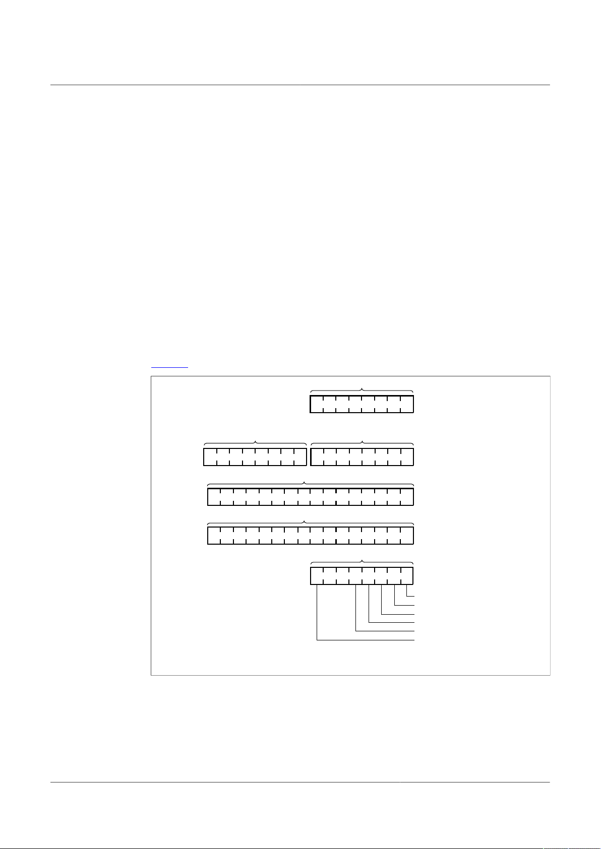
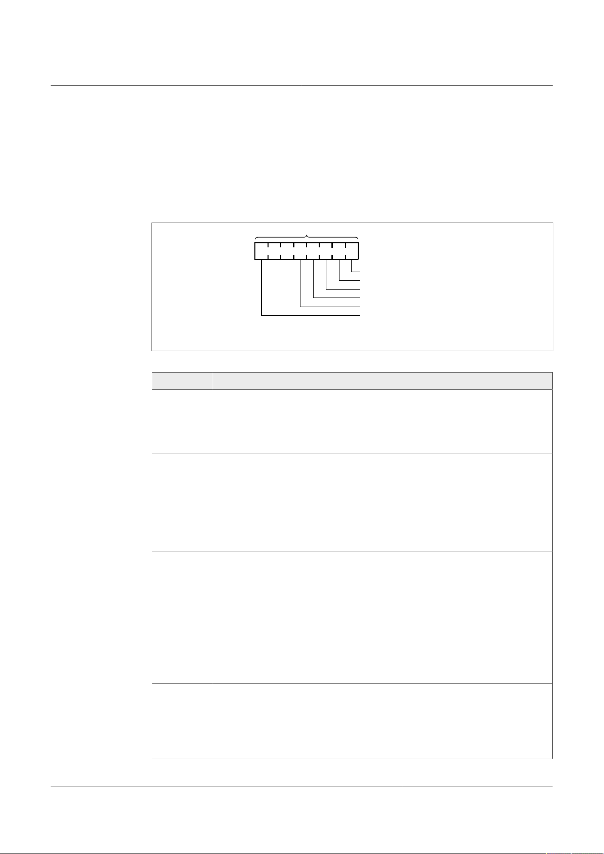
7 Pinning information
This section describes the pin layout and general function of each pin.
7.1 Pinout
UM11227
NTM88 family of tire pressure monitor sensors
Figure 3. NTM88 QFN package pinout
7.2 Pin description
Table 5. Pin description
Symbol Pin Function Description
n.c. 1 — Do not connect electrical signals to this pin; solder joint only.
n.c. 2 — Do not connect electrical signals to this pin; solder joint only.
n.c. 3 — Do not connect electrical signals to this pin; solder joint only.
n.c. 4 — Do not connect electrical signals to this pin; solder joint only.
n.c. 5 — Do not connect electrical signals to this pin; solder joint only.
n.c. 6 — Do not connect electrical signals to this pin; solder joint only.
PTA4 7 PTA4 / BKGD PTA4 Pin - The PTA4 pin places the device in the BACKGROUND DEBUG
mode (BDM) to evaluate MCU code and transfer data to/from the internal
memory. If the BKGD/PTA4 pin is held low when the device comes out of a
power-on-reset (POR), the device switches into the ACTIVE BACKGROUND
DEBUG mode (BDM).
The BKGD/PTA4 pin has an internal pullup device or can be connected to
UM11227 All information provided in this document is subject to legal disclaimers. © NXP B.V. 2021. All rights reserved.
User manual Rev. 7 — 29 March 2021
VDD in the application, unless there is a need to enter BDM operation after
the device as been soldered into the PWB. If in-circuit BDM is desired, the
BKGD/PTA4 pin should be connected to VDD through a resistor (~10 kΩ
or greater) which can be over-driven by an external signal. This resistor
reduces the possibility of inadvertently activating the debug mode in the
application due to an EMC event.
When the application programs port A to GPIOs, PTA4 becomes output-only.
11 / 207
Page 12

NXP Semiconductors
UM11227
NTM88 family of tire pressure monitor sensors
Table 5. Pin description...continued
Symbol Pin Function Description
RST_B 8 Reset / V
programming voltage
VDDA 9 Analog supply The analog circuits operate from a single power supply connected to the unit
GND 10 Digital and analog
ground
VDD 11 Digital supply The digital circuits operate from a single power supply connected to the unit
VREG 12 1.8 V regulation The internal regulator for the RF analog circuits requires an external
PTB0 13 PTB0 / TPMCH0 /
AD3
PTA3 14 PTA3 / KBI3 / MOSI The PTA[3] pin is a general-purpose I/O pin. The pulldown devices can only
PTA2 15 PTA2 / KBI2 / MISO The PTA[2] pin is a general-purpose I/O pin. The pulldown devices can only
PP
The RST_B pin is used for test and establishing the BDM condition and
providing the programming voltage source to the internal FLASH memory.
This pin can also be used to direct to the MCU to the reset vector.
The RST_B pin has an internal pullup device and can be connected to VDD
in the application unless there is a need to enter BDM operation after the
device as been soldered to the PWB. If in-circuit BDM is desired, the RST_B
pin can be left unconnected; but should be connected to VDD through a low
impedance resistor (<10 kΩ) which can be over-driven by an external signal.
This low impedance resistor reduces the possibility of getting into the debug
mode in the application due to an EMC event.
Activation of the external reset function occurs when the voltage on the
RST_B pin goes below 0.3 × VDD for at least 100 ns before rising above
0.7 × VDD.
through the VDDA pin. VDDA is the positive supply and GND is the ground.
The conductors to the power supply should be connected to the VDDA and
GND pins and locally decoupled.
Care should be taken to reduce measurement signal noise by separating
the VDD, GND, VDDA, and RFGND pins using a “star” connection such
that each metal trace does not share any load currents with other external
devices.
The digital circuits operate from a single power supply connected to the unit
through the VDD and GND pins. GND is the ground. Care should be taken to
reduce measurement signal noise by separating the GND and RFGND pins
using a “star” connection such that each metal trace does not share any load
currents with other external devices.
through the VDD and GND pins. VDD is the positive supply. The conductors
to the power supply should be connected to the VDD and GND pins and
locally decoupled.
stabilization capacitor to GND.
The PTB[0] pin is a general-purpose I/O pin. This pin can be configured
as a nominal bidirectional I/O pin with programmable pullup devices. User
software must configure the general-purpose I/O pin (PTB[1:0]) so that they
do not result in “floating” inputs. PTB0 can be mapped to TPM channel 0, or
to ADC channel 3.
be activated if the wake-up interrupt capability is enabled. User software
must configure the general-purpose I/O pins so that they do not result in
“floating” inputs. PTA[3] maps to keyboard interrupt function bit [3]. When SPI
is enabled, PTA[3] serves as MOSI.
be activated if the wake-up interrupt capability is enabled. User software
must configure the general-purpose I/O pins so that they do not result in
“floating” inputs. PTA[2] maps to keyboard interrupt function bit [2]. When SPI
is enabled, PTA[2] serves as MISO.
UM11227 All information provided in this document is subject to legal disclaimers. © NXP B.V. 2021. All rights reserved.
User manual Rev. 7 — 29 March 2021
12 / 207
Page 13

NXP Semiconductors
UM11227
NTM88 family of tire pressure monitor sensors
Table 5. Pin description...continued
Symbol Pin Function Description
PTA1 16 PTA1 / KBI1 / SCLK The PTA[1] pin is a general-purpose I/O pin. The pulldown devices can only
be activated if the wake-up interrupt capability is enabled. User software
must configure the general-purpose I/O pins so that they do not result in
“floating” inputs. PTA[1] maps to keyboard interrupt function bit [1]. When SPI
is enabled, PTA[1] serves as SCLK
RFGND 17 RF ground Power in the RF output amplifier is returned to the supply through the
RFGND pin. This conductor should be connected to the power supply using
a “star” connection such that each metal trace does not share any load
currents with other supply pins.
RFOUT 18 RF output The RFOUT pin is the RF energy data supplied by the unit to an external
antenna.
PTA0 19 PTA0 / KBI0 / SS_B /
IRQ
X1 20 RF crystal input The X1 pin is for an external 26 MHz crystal to be used by the internal PLL
X0 21 RF crystal output The X0 pin is for an external 26 MHz crystal to be used by the internal PLL
PTB1 22 PTB1 / TPMCH1 /
AD4
LFB 23 LF input '-' The LF[A:B] pins can be used by the LF receiver (LFR) as one differential
LFA 24 LF input '+' The LF[A:B] pins can be used by the LF receiver (LFR) as one differential
The PTA[0] pin is a general-purpose I/O pin. PTA[0] can be configured as a
normal bidirectional I/O pin with programmable pullup or pulldown devices
and/or wake-up interrupt capability. PTA[0] can be configured for external
interrupt (IRQ). The pulldown devices can only be activated if the wake-up
interrupt capability is enabled. User software must configure the generalpurpose I/O pins so that they do not result in “floating” inputs. PTA[0] maps
to keyboard interrupt function bit [0]. When SPI is enabled, PTA0 serves as
SS_B.
for creating the carrier frequencies and data rates for the RF pin.
for creating the carrier frequencies and data rates for the RF pin.
The PTB[1] pin is a general-purpose I/O pin. This pin can be configured
as a nominal bidirectional I/O pin with programmable pullup devices. User
software must configure the general-purpose I/O pins (PTB[1:0]) so that they
do not result in “floating” inputs. PTB1 can be mapped to TPM channel 1, or
to ADC channel 4.
input channel for sensing low-level signals from an external low frequency
(LF) coil. The external LF coil should be connected between the LF[A] and
the LF[B] pins.
Signaling into the LFR pins can place the unit into various diagnostic or
operational modes. The LFR is comprised of the detector and the decoder.
Each LF[A:B] pin always has an impedance of approximately 500 kΩ to GND
due to the LFR input circuitry.
The LFA/LFB pins are used by the LFR when the LFEN control bit is set and
are not functional when the LFEN control bit is clear.
UM11227 All information provided in this document is subject to legal disclaimers. © NXP B.V. 2021. All rights reserved.
User manual Rev. 7 — 29 March 2021
13 / 207
Page 14
NXP Semiconductors
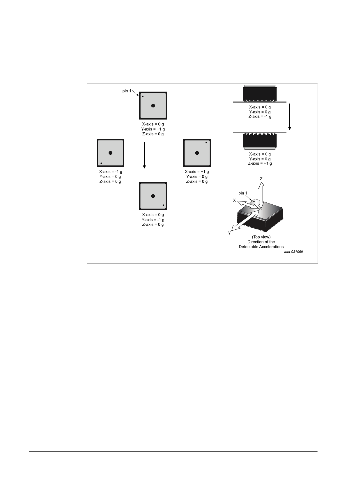
Gravity
Gravity
7.3 Orientation
UM11227
NTM88 family of tire pressure monitor sensors
Figure 4. NTM88 orientation at rest.
8 Central processing unit
8.1 Introduction
This section provides summary information about the registers, addressing modes, and
instruction set of the CPU of the HCS08 Family. For a more detailed discussion, refer to
the HCS08 Family Reference Manual, volume 1, NXP Semiconductor document order
number HCS08RMV1/D.
The HCS08 CPU is fully source- and object-code-compatible with the M68HC08 CPU.
Several instructions and enhanced addressing modes were added to improve C compiler
efficiency and to support a new BACKGROUND DEBUG system which replaces the
monitor mode of earlier M68HC08 microcontrollers (MCU).
8.2 Features
Features of the HCS08 CPU include:
• Object code fully upward compatible with M68HC05 and M68HC08 Families
• All registers and memory are mapped to a single 64 kB address space
• 16-bit stack pointer (any size stack anywhere in 64 kB address space)
• 16-bit index register (H:X) with powerful indexed addressing modes
• 8-bit accumulator (A)
• Many instructions treat X as a second general-purpose 8-bit register
UM11227 All information provided in this document is subject to legal disclaimers. © NXP B.V. 2021. All rights reserved.
User manual Rev. 7 — 29 March 2021
14 / 207
Page 15
NXP Semiconductors
aaa-028004
accumulator
A
index register (low)index register (high)
16-bit index register H:X
XH
stack pointer
condition code register
V 1 1 H I N Z C
SP
CCR
Carry
Zero
Interrupt mask
Two's complement overflow
Half-carry (from bit 3)
Negative
program counter pointer
PC
• Seven addressing modes:
– Inherent — Operands in internal registers
– Relative — 8-bit signed offset to branch destination
– Immediate — Operand in next object code byte(s)
– Direct — Operand in memory at 0x0000–0x00FF
– Extended — Operand anywhere in 64 kB address space
– Indexed relative to H:X — Five submodes including auto-increment
– Indexed relative to SP — Improves C efficiency dramatically
• Memory-to-memory data move instructions with four address mode combinations
• Overflow, half-carry, negative, zero, and carry condition codes support conditional
branching on the results of signed, unsigned, and binary-coded decimal (BCD)
operations
• Efficient bit manipulation instructions
• Fast 8-bit by 8-bit multiply and 16-bit by 8-bit divide instructions
• STOP and WAIT instructions to invoke low-power operating modes
8.3 Programmer’s model and CPU registers
UM11227
NTM88 family of tire pressure monitor sensors
Figure 5 shows the five CPU registers. CPU registers are not part of the memory map.
Figure 5. CPU registers
8.3.1 Accumulator (A)
The A accumulator is a general-purpose 8-bit register. One operand input to the
arithmetic logic unit (ALU) is connected to the accumulator and the ALU results are often
stored into the A accumulator after arithmetic and logical operations. The accumulator
can be loaded from memory using various addressing modes to specify the address
UM11227 All information provided in this document is subject to legal disclaimers. © NXP B.V. 2021. All rights reserved.
User manual Rev. 7 — 29 March 2021
15 / 207
Page 16

NXP Semiconductors
where the loaded data comes from, or the contents of A can be stored to memory using
various addressing modes to specify the address where data from A will be stored.
Reset has no effect on the contents of the A accumulator.
8.3.2 Index register (H:X)
This 16-bit register is actually two separate 8-bit registers (H and X), which often work
together as a 16-bit address pointer where H holds the upper byte of an address and X
holds the lower byte of the address. All indexed addressing mode instructions use the
full 16-bit value in H:X as an index reference pointer; however, for compatibility with the
earlier M68HC05 Family, some instructions operate only on the low-order 8-bit half (X).
Many instructions treat X as a second general-purpose 8-bit register that can be used
to hold 8-bit data values. X can be cleared, incremented, decremented, complemented,
negated, shifted, or rotated. Transfer instructions allow data to be transferred from A or
transferred to A where arithmetic and logical operations can then be performed.
For compatibility with the earlier M68HC05 Family, H is forced to 0x00 during reset.
Reset has no effect on the contents of X.
UM11227
NTM88 family of tire pressure monitor sensors
8.3.3 Stack pointer (SP)
This 16-bit address pointer register points at the next available location on the automatic
last-in-first-out (LIFO) stack. The stack may be located anywhere in the 64 kB address
space that has RAM and can be any size up to the amount of available RAM. The stack
is used to automatically save the return address for subroutine calls, the return address
and CPU registers during interrupts, and for local variables. The AIS (add immediate to
stack pointer) instruction adds an 8-bit signed immediate value to SP. This is most often
used to allocate or deallocate space for local variables on the stack.
SP is forced to 0x00FF at reset for compatibility with the earlier M68HC05 Family. HCS08
programs normally change the value in SP to the address of the last location (highest
address) in on-chip RAM during reset initialization to free up direct page RAM (from the
end of the on-chip registers to 0x00FF).
The RSP (reset stack pointer) instruction was included for compatibility with the
M68HC05 Family and is seldom used in new HCS08 programs because it only affects
the low-order half of the stack pointer.
8.3.4 Program counter (PC)
The program counter is a 16-bit register that contains the address of the next instruction
or operand to be fetched.
During normal program execution, the program counter automatically increments to the
next sequential memory location every time an instruction or operand is fetched. Jump,
branch, interrupt, and return operations load the program counter with an address other
than that of the next sequential location. This is called a change-of-flow.
During reset, the program counter is loaded with the reset vector that is located at
0xFFFE and 0xFFFF. The vector stored there is the address of the first instruction that
will be executed after exiting the reset state.
UM11227 All information provided in this document is subject to legal disclaimers. © NXP B.V. 2021. All rights reserved.
User manual Rev. 7 — 29 March 2021
16 / 207
Page 17
NXP Semiconductors
aaa-028005
condition code register
V 1 1 H I N Z C
CCR
Carry
Zero
Interrupt mask
Two's complement overflow
Half-carry (from bit 3)
Negative
8.3.5 Condition code register (CCR)
The 8-bit condition code register contains the interrupt mask (I) and five flags that
indicate the results of the instruction just executed. Bits 6 and 5 are set permanently to
1. The following paragraphs describe the functions of the condition code bits in general
terms. For a more detailed explanation of how each instruction sets the CCR bits, refer to
the HCS08 Family Reference Manual, volume 1, NXP Semiconductors document order
number HCS08RMv1.
Figure 6. Condition code register
UM11227
NTM88 family of tire pressure monitor sensors
Table 6. CCR register field descriptions
Field Description
Two’s Complement Overflow Flag — The CPU sets the overflow flag when a two’s
7
V
complement overflow occurs. The signed branch instructions BGT, BGE, BLE, and
BLT use the overflow flag.
0 No overflow
1 Overflow
Half-Carry Flag — The CPU sets the half-carry flag when a carry occurs between
accumulator bits 3 and 4 during an add-without-carry (ADD) or add-with-carry
(ADC) operation. The half-carry flag is required for binary-coded decimal (BCD)
4
H
arithmetic operations. The DAA instruction uses the states of the H and C
condition code bits to automatically add a correction value to the result from a
previous ADD or ADC on BCD operands to correct the result to a valid BCD value.
0 No carry between bits 3 and 4
1 Carry between bits 3 and 4
Interrupt Mask Bit — When the interrupt mask is set, all maskable CPU interrupts
are disabled. CPU interrupts are enabled when the interrupt mask is cleared.
When a CPU interrupt occurs, the interrupt mask is set automatically after the CPU
registers are saved on the stack, but before the first instruction of the interrupt
3
I
service routine is executed.
Interrupts are not recognized at the instruction boundary after any instruction that
clears I (CLI or TAP). This ensures that the next instruction after a CLI or TAP will
always be executed without the possibility of an intervening interrupt, provided I
was set.
0 Interrupts enabled
1 Interrupts disabled
Negative Flag — The CPU sets the negative flag when an arithmetic operation,
logic operation, or data manipulation produces a negative result, setting bit 7 of the
2
N
result. Simply loading or storing an 8-bit, or 16-bit value causes N to be set if the
most significant bit of the loaded or stored value was 1.
0 Non-negative result
1 Negative result
UM11227 All information provided in this document is subject to legal disclaimers. © NXP B.V. 2021. All rights reserved.
User manual Rev. 7 — 29 March 2021
17 / 207
Page 18

NXP Semiconductors
Table 6. CCR register field descriptions...continued
8.4 Addressing modes
Addressing modes define the way the CPU accesses operands and data. In the HCS08,
all memory, status and control registers, and input/output (I/O) ports share a single 64
kB linear address space so a 16-bit binary address can uniquely identify any memory
location. This arrangement means that the same instructions that access variables in
RAM can also be used to access I/O and control registers or nonvolatile program space.
Field Description
Zero Flag — The CPU sets the zero flag when an arithmetic operation, logic
operation, or data manipulation produces a result of 0x00 or 0x0000. Simply
1
Z
0
C
loading or storing an 8-bit, or 16-bit value causes Z to be set if the loaded or stored
value was all 0s.
0 Non-zero result
1 Zero result
Carry/Borrow Flag — The CPU sets the carry/borrow flag when an addition
operation produces a carry out of bit 7 of the accumulator or when a subtraction
operation requires a borrow. Some instructions — such as bit test and branch,
shift, and rotate — also clear or set the carry/borrow flag.
0 No carry out of bit 7
1 Carry out of bit 7
UM11227
NTM88 family of tire pressure monitor sensors
Some instructions use more than one addressing mode. For instance, move instructions
use one addressing mode to specify the source operand and a second addressing mode
to specify the destination address. Instructions such as BRCLR, BRSET, CBEQ, and
DBNZ use one addressing mode to specify the location of an operand for a test and then
use relative addressing mode to specify the branch destination address when the tested
condition is true. For BRCLR, BRSET, CBEQ, and DBNZ, the addressing mode listed in
the instruction set tables is the addressing mode needed to access the operand to be
tested, and relative addressing mode is implied for the branch destination.
8.4.1 Inherent addressing mode (INH)
In this addressing mode, operands needed to complete the instruction (if any) are located
within CPU registers so the CPU does not need to access memory to get any operands.
8.4.2 Relative addressing mode (REL)
Relative addressing mode is used to specify the destination location for branch
instructions. A signed 8-bit offset value is located in the memory location immediately
following the opcode. During execution, if the branch condition is true, the signed offset
is sign-extended to a 16-bit value and is added to the current contents of the program
counter, which causes program execution to continue at the branch destination address.
8.4.3 Immediate addressing mode (IMM)
In immediate addressing mode, the operand needed to complete the instruction is
included in the object code immediately following the instruction opcode in memory.
In the case of a 16-bit immediate operand, the high-order byte is located in the next
memory location after the opcode, and the low-order byte is located in the next memory
location after that.
UM11227 All information provided in this document is subject to legal disclaimers. © NXP B.V. 2021. All rights reserved.
User manual Rev. 7 — 29 March 2021
18 / 207
Page 19

NXP Semiconductors
8.4.4 Direct addressing mode (DIR)
In direct addressing mode, the instruction includes the low-order 8 bits of an address
in the direct page (0x0000–0x00FF). During execution, a 16-bit address is formed by
concatenating an implied 0x00 for the high-order half of the address and the direct
address from the instruction to get the 16-bit address where the desired operand is
located. DIR is faster and more memory efficient than specifying a complete 16-bit
address for the operand.
8.4.5 Extended addressing mode (EXT)
In extended addressing mode, the full 16-bit address of the operand is located in the next
2 bytes of program memory after the opcode (high byte first).
8.4.6 Indexed addressing mode
Indexed addressing mode has seven variations including five that use the 16-bit H:X
index register pair and two that use the stack pointer as the base reference.
8.4.6.1 Indexed, no offset (IX)
UM11227
NTM88 family of tire pressure monitor sensors
This variation of indexed addressing uses the 16-bit value in the H:X index register pair
as the address of the operand needed to complete the instruction.
8.4.6.2 Indexed, no offset with post increment (IX+)
This variation of indexed addressing uses the 16-bit value in the H:X index register pair
as the address of the operand needed to complete the instruction. The index register
pair is then incremented (H:X = H:X + 0x0001) after the operand has been fetched. This
addressing mode is only used for MOV and CBEQ instructions.
8.4.6.3 Indexed, 8-bit offset (IX1)
This variation of indexed addressing uses the 16-bit value in the H:X index register pair
plus an unsigned 8-bit offset included in the instruction as the address of the operand
needed to complete the instruction.
8.4.6.4 Indexed, 8-bit offset with post increment (IX1+)
This variation of indexed addressing uses the 16-bit value in the H:X index register pair
plus an unsigned 8-bit offset included in the instruction as the address of the operand
needed to complete the instruction. The index register pair is then incremented (H:X =
H:X + 0x0001) after the operand has been fetched. This addressing mode is used only
for the CBEQ instruction.
8.4.6.5 Indexed, 16-bit offset (IX2)
This variation of indexed addressing uses the 16-bit value in the H:X index register pair
plus a 16-bit offset included in the instruction as the address of the operand needed to
complete the instruction.
UM11227 All information provided in this document is subject to legal disclaimers. © NXP B.V. 2021. All rights reserved.
User manual Rev. 7 — 29 March 2021
19 / 207
Page 20

NXP Semiconductors
8.4.6.6 SP-Relative, 8-bit offset (SP1)
This variation of indexed addressing uses the 16-bit value in the stack pointer (SP) plus
an unsigned 8-bit offset included in the instruction as the address of the operand needed
to complete the instruction.
8.4.6.7 SP-Relative, 16-bit offset (SP2)
This variation of indexed addressing uses the 16-bit value in the stack pointer (SP) plus a
16-bit offset included in the instruction as the address of the operand needed to complete
the instruction.
8.5 Special operations
The CPU performs a few special operations that are similar to instructions but do not
have opcodes like other CPU instructions. In addition, a few instructions such as STOP
and WAIT directly affect other MCU circuitry. This section provides additional information
about these operations.
8.5.1 Reset sequence
UM11227
NTM88 family of tire pressure monitor sensors
Reset can be caused by a power-on-reset (POR) event, internal conditions such as the
COP (computer operating properly) watchdog, or by assertion of an external active-low
reset pin. When a reset event occurs, the CPU immediately stops whatever it is doing
(the MCU does not wait for an instruction boundary before responding to a reset event).
For a more detailed discussion about how the MCU recognizes resets and determines
the source, see Section 10.11 "Reset, interrupts and system configuration".
The reset event is considered concluded when the sequence to determine whether the
reset came from an internal source is done and when the reset pin is no longer asserted.
At the conclusion of a reset event, the CPU performs a 6-cycle sequence to fetch the
reset vector from 0xFFFE and 0xFFFF and to fill the instruction queue in preparation for
execution of the first program instruction.
8.5.2 Interrupt sequence
When an interrupt is requested, the CPU completes the current instruction before
responding to the interrupt. At this point, the program counter is pointing at the start of
the next instruction, which is where the CPU should return after servicing the interrupt.
The CPU responds to an interrupt by performing the same sequence of operations as
for a software interrupt (SWI) instruction, except the address used for the vector fetch is
determined by the highest priority interrupt that is pending when the interrupt sequence
started.
The CPU sequence for an interrupt is:
1. Store the contents of PCL, PCH, X, A, and CCR on the stack, in that order.
2. Set the I bit in the CCR.
3. Fetch the high-order half of the interrupt vector.
4. Fetch the low-order half of the interrupt vector.
5. Delay for one free bus cycle.
6. Fetch 3 bytes of program information, starting at the address indicated by the interrupt
vector, to fill the instruction queue in preparation for execution of the first instruction in
the interrupt service routine.
UM11227 All information provided in this document is subject to legal disclaimers. © NXP B.V. 2021. All rights reserved.
User manual Rev. 7 — 29 March 2021
20 / 207
Page 21

NXP Semiconductors
After the CCR contents are pushed onto the stack, the I bit in the CCR is set to prevent
other interrupts while in the interrupt service routine. Although it is possible to clear the I
bit with an instruction in the interrupt service routine, this would allow nesting of interrupts
(which is not recommended because it leads to programs that are difficult to debug and
maintain).
For compatibility with the earlier M68HC05 MCUs, the high-order half of the H:X index
register pair (H) is not saved on the stack as part of the interrupt sequence. The user
must use a PSHH instruction at the beginning of the service routine to save H and then
use a PULH instruction just before the RTI that ends the interrupt service routine. It is not
necessary to save H if you are certain that the interrupt service routine does not use any
instructions or auto-increment addressing modes that might change the value of H.
The software interrupt (SWI) instruction is like a hardware interrupt except that it is not
masked by the global I bit in the CCR and it is associated with an instruction opcode
within the program so it is not asynchronous to program execution.
8.5.3 WAIT mode operation
The WAIT instruction enables interrupts by clearing the I bit in the CCR. It then halts
the clocks to the CPU to reduce overall power consumption while the CPU is waiting for
the interrupt or reset event that will wake the CPU from WAIT mode. When an interrupt
or reset event occurs, the CPU clocks resume and the interrupt or reset event are
processed normally.
UM11227
NTM88 family of tire pressure monitor sensors
If a serial BACKGROUND command is issued to the MCU through the BACKGROUND
DEBUG interface while the CPU is in WAIT mode, CPU clocks resume and the CPU
enters ACTIVE BACKGROUND mode where other serial BACKGROUND commands
can be processed. This ensures that a host development system can still gain access to
a target MCU even if it is in WAIT mode.
8.5.4 STOP mode operation
Usually, all system clocks, including the crystal oscillator (when used), are halted during
STOP mode to minimize power consumption. In such systems, external circuitry is
needed to control the time spent in STOP mode and to issue a signal to wake up the
target MCU when it is time to resume processing. Unlike the earlier M68HC05 and
M68HC08 MCUs, the HCS08 can be configured to keep a minimum set of clocks running
in STOP mode. This optionally allows an internal periodic signal to wake the target MCU
from STOP mode.
When a host debug system is connected to the BACKGROUND DEBUG pin (BKGD) and
the ENBDM control bit has been set by a serial command through the BACKGROUND
interface (or because the MCU was reset into ACTIVE BACKGROUND mode), the
oscillator is forced to remain active when the MCU enters STOP mode. In this case, if
a serial BACKGROUND command is issued to the MCU through the BACKGROUND
DEBUG interface while the CPU is in STOP mode, CPU clocks resume and the CPU
enters ACTIVE BACKGROUND mode where other serial BACKGROUND commands
can be processed. This ensures that a host development system can still gain access to
a target MCU even if it is in STOP mode.
Recovery from STOP mode depends on the particular HCS08 and whether the oscillator
was stopped in STOP mode. See Section 10.8 "Modes of operation" for more details.
UM11227 All information provided in this document is subject to legal disclaimers. © NXP B.V. 2021. All rights reserved.
User manual Rev. 7 — 29 March 2021
21 / 207
Page 22

NXP Semiconductors
8.5.5 BGND instruction
The BGND instruction is new to the HCS08 compared to the M68HC08. BGND would
not be used in normal user programs because it forces the CPU to stop processing
user instructions and enter the ACTIVE BACKGROUND mode. The only way to resume
execution of the user program is through reset or by a host debug system issuing a GO,
TRACE1, or TAGGO serial command through the BACKGROUND DEBUG interface.
Software-based breakpoints can be set by replacing an opcode at the desired breakpoint
address with the BGND opcode. When the program reaches this breakpoint address, the
CPU is forced to ACTIVE BACKGROUND mode rather than continuing the user program.
8.6 HCS08 instruction set summary
8.6.1 Instruction set summary nomenclature
The nomenclature listed here is used in the instruction descriptions in Table 7.
8.6.2 Operators
UM11227
NTM88 family of tire pressure monitor sensors
( ) = Contents of register or memory location shown inside parentheses
← = Is loaded with (read: "gets")
& = Boolean AND
| = Boolean OR
= Boolean exclusive-OR
⊕
× = Multiply
÷ = Divide
: = Concatenate
+ = Add
– = Negate (two’s complement)
8.6.3 CPU registers
A = Accumulator
CCR = Condition code register
H = Index register, higher order (most significant) 8 bits
X = Index register, lower order (least significant) 8 bits
PC = Program counter
PCH = Program counter, higher order (most significant) 8 bits
PCL = Program counter, lower order (least significant) 8 bits
SP = Stack pointer
8.6.4 Memory and addressing
M = A memory location or absolute data, depending on addressing mode
UM11227 All information provided in this document is subject to legal disclaimers. © NXP B.V. 2021. All rights reserved.
User manual Rev. 7 — 29 March 2021
22 / 207
Page 23

NXP Semiconductors
M:M + 0x0001 = A 16-bit value in two consecutive memory locations. The higher order
(most significant) 8 bits are located at the address of M, and the lower order (least
significant) 8 bits are located at the next higher sequential address.
8.6.5 Condition code register (CCR) bits
V = Two’s complement overflow indicator, bit 7
H = Half carry, bit 4
I = Interrupt mask, bit 3
N = Negative indicator, bit 2
Z = Zero indicator, bit 1
C = Carry/borrow, bit 0 (carry out of bit 7)
8.6.6 CCR activity notation
– = Bit not affected
0 = Bit forced to 0
1 = Bit forced to 1
Þ = Bit set or cleared according to results of operation
U = Undefined after the operation
UM11227
NTM88 family of tire pressure monitor sensors
8.6.7 Machine coding notation
dd = Low-order 8 bits of a direct address 0x0000–0x00FF (high byte assumed to be 0x00)
ee = Upper 8 bits of 16-bit offset
ff = Lower 8 bits of 16-bit offset or 8-bit offset
ii = One byte of immediate data
jj = High-order byte of a 16-bit immediate data value
kk = Low-order byte of a 16-bit immediate data value
hh = High-order byte of 16-bit extended address
ll = Low-order byte of 16-bit extended address
rr = Relative offset
8.6.8 Source form
Everything in the source forms columns, except expressions in italic characters, is literal
information that must appear in the assembly source file exactly as shown. The initial
3- to 5-letter mnemonic is always a literal expression. All commas, pound signs (#),
parentheses, and plus signs (+) are literal characters.
n — Any label or expression that evaluates to a single integer in the range 0–7
opr8i — Any label or expression that evaluates to an 8-bit immediate value
opr16i — Any label or expression that evaluates to a 16-bit immediate value
UM11227 All information provided in this document is subject to legal disclaimers. © NXP B.V. 2021. All rights reserved.
User manual Rev. 7 — 29 March 2021
23 / 207
Page 24

NXP Semiconductors
opr8a — Any label or expression that evaluates to an 8-bit value. The instruction treats
this 8-bit value as the low order 8 bits of an address in the direct page of the 64 kB
address space (0x00xx).
opr16a — Any label or expression that evaluates to a 16-bit value. The instruction treats
this value as an address in the 64 kB address space.
oprx8 — Any label or expression that evaluates to an unsigned 8-bit value, used for
indexed addressing
oprx16 — Any label or expression that evaluates to a 16-bit value. Because the HCS08
has a 16-bit address bus, this can be either a signed or an unsigned value.
rel — Any label or expression that refers to an address that is within –128 to +127
locations from the next address after the last byte of object code for the current
instruction. The assembler calculates the 8-bit signed offset and include it in the object
code for this instruction.
8.6.9 Address modes
INH = Inherent (no operands)
IMM = 8-bit or 16-bit immediate
DIR = 8-bit direct
EXT = 16-bit extended
IX = 16-bit indexed no offset
IX+ = 16-bit indexed no offset, post increment (CBEQ and MOV only)
IX1 = 16-bit indexed with 8-bit offset from H:X
IX1+ = 16-bit indexed with 8-bit offset, post increment (CBEQ only)
IX2 = 16-bit indexed with 16-bit offset from H:X
rel = 8-bit relative offset
SP1 = Stack pointer with 8-bit offset
SP2 = Stack pointer with 16-bit offset
UM11227
NTM88 family of tire pressure monitor sensors
Table 7. HCS08 instruction set summary
Effect
Source Form Operation Description
ADC #opr8i
ADC opr8a
ADC opr16a
ADC oprx16,X
ADC oprx8,X
ADC,X
ADC oprx16,SP
ADC oprx8,SP
UM11227 All information provided in this document is subject to legal disclaimers. © NXP B.V. 2021. All rights reserved.
User manual Rev. 7 — 29 March 2021
Add with Carry A ← (A) + (M) + (C) Þ Þ – Þ Þ Þ
on CCR
V H I N Z C
Address
Mode
IMM
DIR
EXT
IX2
IX1
IX
SP2
SP1
Opcode Operand
A9
ii
B9
dd
C9
hh ll
D9
ee ff
E9
ff
F9
9ED9
ee ff
9EE9
ff
Bus
Cycles
[1]
2
3
4
4
3
3
5
4
24 / 207
Page 25

NXP Semiconductors
b0
b7
C
0
aaa-028006
b0
b7
C
aaa-028007
UM11227
NTM88 family of tire pressure monitor sensors
Table 7. HCS08 instruction set summary...continued
Effect
Source Form Operation Description
on CCR
V H I N Z C
ADD #opr8i
ADD opr8a
ADD opr16a
ADD oprx16,X
ADD oprx8,X
Add without Carry A ← (A) + (M) Þ Þ – Þ Þ Þ
ADD ,X
ADD oprx16,SP
ADD oprx8,SP
SP ← (SP) + (M)
M is sign extended to a
16-bit value
H:X ← (H:X) + (M)
M is sign extended to a
16-bit value
– – – – – – IMM A7 ii
– – – – – – IMM AF ii
AIS #opr8i
AIX #opr8i
Add Immediate
Value (Signed) to
Stack Pointer
Add Immediate
Value (Signed)
to Index Register
(H:X)
AND #opr8i
AND opr8a
AND opr16a
AND oprx16,X
AND oprx8,X
Logical AND A ← (A) & (M) 0 – – Þ Þ –
AND ,X
AND oprx16,SP
AND oprx8,SP
ASL opr8a
ASLA
ASLX
ASL oprx8,X
ASL ,X
ASL oprx8,SP
ASR opr8a
ASRA
ASRX
ASR oprx8,X
ASR ,X
ASR oprx8,SP
BCC rel
BCLR n,opr8a
BCS rel
Arithmetic Shift Left
(Same as LSL)
Arithmetic Shift
Right
Branch if Carry Bit
Clear
Clear Bit n in
Memory
Branch if Carry Bit
Set (Same as BLO)
Þ – – Þ Þ Þ
Þ – – Þ Þ Þ
Branch if (C) = 0 – – – – – – rel
Mn ← 0 – – – – – –
Branch if (C) = 1 – – – – – – rel
BEQ rel Branch if Equal Branch if (Z) = 1 – – – – – – rel 27 rr 3
Address
Mode
IMM
DIR
EXT
IX2
IX1
IX
SP2
SP1
IMM
DIR
EXT
IX2
IX1
IX
SP2
SP1
DIR
INH
INH
IX1
IX
SP1
DIR
INH
INH
IX1
IX
SP1
DIR (b0)
DIR (b1)
DIR (b2)
DIR (b3)
DIR (b4)
DIR (b5)
DIR (b6)
DIR (b7)
Opcode Operand
AB
ii
BB
dd
CB
hh ll
DB
ee ff
EB
ff
FB
9EDB
ee ff
9EEB
ff
A4
ii
B4
dd
C4
hh ll
D4
ee ff
E4
ff
F4
9ED4
ee ff
9EE4
ff
38
dd
48
58
68
ff
78
9E68
ff
37
dd
47
57
67
ff
77
9E67
ff
24 rr 3
11
dd
13
dd
15
dd
17
dd
19
dd
1B
dd
1D
dd
1F
dd
25 rr 3
Cycles
Bus
[1]
2
3
4
4
3
3
5
4
2
2
2
3
4
4
3
3
5
4
5
1
1
5
4
6
5
1
1
5
4
6
5
5
5
5
5
5
5
5
UM11227 All information provided in this document is subject to legal disclaimers. © NXP B.V. 2021. All rights reserved.
User manual Rev. 7 — 29 March 2021
25 / 207
Page 26

NXP Semiconductors
UM11227
NTM88 family of tire pressure monitor sensors
Table 7. HCS08 instruction set summary...continued
Effect
Source Form Operation Description
BGE rel
BGND
BGT rel
BHCC rel
BHCS rel
BHI rel Branch if Higher Branch if (C) | (Z) = 0 – – – – – – rel 22 rr 3
BHS rel
BIH rel
BIL rel
BIT #opr8i
BIT opr8a
BIT opr16a
BIT oprx16,X
BIT oprx8,X
BIT ,X
BIT oprx16,SP
BIT oprx8,SP
BLE rel
BLO rel
BLS rel
BLT rel
BMC rel
BMI rel Branch if Minus Branch if (N) = 1 – – – – – – rel 2B rr 3
BMS rel
BNE rel Branch if Not Equal Branch if (Z) = 0 – – – – – – rel 26 rr 3
BPL rel Branch if Plus Branch if (N) = 0 – – – – – – rel 2A rr 3
BRA rel Branch Always No Test – – – – – – rel 20 rr 3
Branch if Greater
Than or Equal To
(Signed Operands)
Enter ACTIVE
BACK-GROUND if
ENBDM = 1
Branch if Greater
Than (Signed
Operands)
Branch if Half Carry
Bit Clear
Branch if Half Carry
Bit Set
Branch if Higher or
Same (Same as
BCC)
Branch if IRQ Pin
High
Branch if IRQ Pin
Low
Bit Test
Branch if Less Than
or Equal To (Signed
Operands)
Branch if Lower
(Same as BCS)
Branch if Lower or
Same
Branch if Less Than
(Signed Operands)
Branch if Interrupt
Mask Clear
Branch if Interrupt
Mask Set
Branch if (N ⊕ V) = 0
Waits For and
Processes BDM
Commands Until GO,
TRACE1, or TAGGO
Branch if (Z) | (N ⊕ V)
= 0
Branch if (H) = 0 – – – – – – rel
Branch if (H) = 1 – – – – – – rel
Branch if (C) = 0 – – – – – – rel
Branch if IRQ pin = 1 – – – – – – rel
Branch if IRQ pin = 0 – – – – – – rel
(A) & (M)
(CCR Updated but
Operands
Not Changed)
Branch if (Z) | (N ⊕ V)
= 1
Branch if (C) = 1 – – – – – – rel
Branch if (C) | (Z) = 1 – – – – – – rel
Branch if (N ⊕ V ) = 1
Branch if (I) = 0 – – – – – – rel
Branch if (I) = 1 – – – – – – rel
on CCR
V H I N Z C
– – – – – – rel
– – – – – – INH
– – – – – – rel
0 – – Þ Þ –
– – – – – – rel
– – – – – – rel
Address
Mode
IMM
DIR
EXT
IX2
IX1
IX
SP2
SP1
Opcode Operand
90 rr 3
82 5+
92 rr 3
28 rr 3
29 rr 3
24 rr 3
2F rr 3
2E rr 3
A5
ii
B5
dd
C5
hh ll
D5
ee ff
E5
ff
F5
9ED5
ee ff
9EE5
ff
93 rr 3
25 rr 3
23 rr 3
91 rr 3
2C rr 3
2D rr 3
Cycles
Bus
[1]
2
3
4
4
3
3
5
4
UM11227 All information provided in this document is subject to legal disclaimers. © NXP B.V. 2021. All rights reserved.
User manual Rev. 7 — 29 March 2021
26 / 207
Page 27

NXP Semiconductors
UM11227
NTM88 family of tire pressure monitor sensors
Table 7. HCS08 instruction set summary...continued
Effect
Source Form Operation Description
BRCLR n,opr8a,rel
BRN rel Branch Never Uses 3 Bus Cycles – – – – – – rel 21 rr 3
BRSET n,opr8a,rel
BSET n,opr8a Set Bit n in Memory Mn ← 1 – – – – – –
BSR rel
CBEQ opr8a,rel
CBEQA #opr8i,rel
CBEQX #opr8i,rel
CBEQ oprx8,X+,rel
CBEQ ,X+,rel
CBEQ oprx8,SP,rel
CLC Clear Carry Bit C ← 0 – – – – – 0 INH 98 1
CLI
CLR opr8a
CLRA
CLRX
CLRH
CLR oprx8,X
CLR ,X
CLR oprx8,SP
Branch if Bit n in
Memory Clear
Branch if Bit n in
Memory Set
Branch to
Subroutine
Compare and
Branch if Equal
Clear Interrupt
Mask Bit
Clear
Branch if (Mn) = 0 – – – – – Þ
Branch if (Mn) = 1 – – – – – Þ
PC ← (PC) + 0x0002
push (PCL); SP ←
(SP) – 0x0001
push (PCH); SP ←
(SP) – 0x0001
PC ← (PC) + rel
Branch if (A) = (M)
Branch if (A) = (M)
Branch if (X) = (M)
Branch if (A) = (M)
Branch if (A) = (M)
Branch if (A) = (M)
I ← 0 – – 0 – – – INH
M ← 0x00
A ← 0x00
X ← 0x00
H ← 0x00
M ← 0x00
M ← 0x00
M ← 0x00
on CCR
V H I N Z C
– – – – – – rel
– – – – – –
0 – – 0 1 –
Address
Mode
DIR (b0)
DIR (b1)
DIR (b2)
DIR (b3)
DIR (b4)
DIR (b5)
DIR (b6)
DIR (b7)
DIR (b0)
DIR (b1)
DIR (b2)
DIR (b3)
DIR (b4)
DIR (b5)
DIR (b6)
DIR (b7)
DIR (b0)
DIR (b1)
DIR (b2)
DIR (b3)
DIR (b4)
DIR (b5)
DIR (b6)
DIR (b7)
DIR
IMM
IMM
IX1+
IX+
SP1
DIR
INH
INH
INH
IX1
IX
SP1
Opcode Operand
01
dd rr
03
dd rr
05
dd rr
07
dd rr
09
dd rr
0B
dd rr
0D
dd rr
0F
dd rr
00
dd rr
02
dd rr
04
dd rr
06
dd rr
08
dd rr
0A
dd rr
0C
dd rr
0E
dd rr
10
dd
12
dd
14
dd
16
dd
18
dd
1A
dd
1C
dd
1E
dd
AD rr 5
31
dd rr
41
ii rr
51
ii rr
61
ff rr
71
rr ff
9E61
rr
9A 1
3F
dd
4F
5F
8C
6F
ff
7F
9E6F
ff
Cycles
Bus
[1]
5
5
5
5
5
5
5
5
5
5
5
5
5
5
5
5
5
5
5
5
5
5
5
5
5
4
4
5
5
6
5
1
1
1
5
4
6
UM11227 All information provided in this document is subject to legal disclaimers. © NXP B.V. 2021. All rights reserved.
User manual Rev. 7 — 29 March 2021
27 / 207
Page 28

NXP Semiconductors
Table 7. HCS08 instruction set summary...continued
Source Form Operation Description
CMP #opr8i
CMP opr8a
CMP opr16a
CMP oprx16,X
CMP oprx8,X
CMP ,X
CMP oprx16,SP
CMP oprx8,SP
COM opr8a
COMA
COMX
COM oprx8,X
COM ,X
COM oprx8,SP
CPHX opr16a
CPHX #opr16i
CPHX opr8a
CPHX oprx8,SP
CPX #opr8i
CPX opr8a
CPX opr16a
CPX oprx16,X
CPX oprx8,X
CPX ,X
CPX oprx16,SP
CPX oprx8,SP
DAA
DBNZ opr8a,rel
DBNZA rel
DBNZX rel
DBNZ oprx8,X,rel
DBNZ ,X,rel
DBNZ oprx8,SP,rel
DEC opr8a
DECA
DECX
DEC oprx8,X
DEC ,X
DEC oprx8,SP
DIV Divide
Compare
Accumulator with
Memory
Complement (One’s
Complement)
Compare Index
Register (H:X) with
Memory
Compare X (Index
Register Low) with
Memory
Decimal Adjust
Accumulator After
ADD or ADC of
BCD Values
Decrement and
Branch if
Not Zero
Decrement
(A) – (M)
(CCR Updated
But Operands Not
Changed)
M ← (M)= 0xFF – (M)
A ← (A) = 0xFF – (A)
X ← (X) = 0xFF – (X)
M ← (M) = 0xFF – (M)
M ← (M) = 0xFF – (M)
M ← (M) = 0xFF – (M)
(H:X) – (M:M +
0x0001)
(CCR Updated
But Operands Not
Changed)
(X) – (M)
(CCR Updated
But Operands Not
Changed)
(A)
10
Decrement A, X, or M
Branch if (result) ≠ 0
DBNZX Affects X Not
H
M ← (M) – 0x01
A ← (A) – 0x01
X ← (X) – 0x01
M ← (M) – 0x01
M ← (M) – 0x01
M ← (M) – 0x01
A ← (H:A) ÷ (X)
H ← Remainder
UM11227
NTM88 family of tire pressure monitor sensors
Effect
on CCR
V H I N Z C
Þ – – Þ Þ Þ
0 – – Þ Þ 1
Þ – – Þ Þ Þ
Þ – – Þ Þ Þ
U – – Þ Þ Þ INH
– – – – – –
Þ – – Þ Þ –
– – – – Þ Þ INH
Address
Mode
IMM
DIR
EXT
IX2
IX1
IX
SP2
SP1
DIR
INH
INH
IX1
IX
SP1
EXT
IMM
DIR
SP1
IMM
DIR
EXT
IX2
IX1
IX
SP2
SP1
DIR
INH
INH
IX1
IX
SP1
DIR
INH
INH
IX1
IX
SP1
Opcode Operand
A1
ii
B1
dd
C1
hh ll
D1
ee ff
E1
ff
F1
9ED1
ee ff
9EE1
ff
33
dd
43
53
63
ff
73
9E63
ff
3E
hh ll
65
jj kk
75
dd
9EF3
ff
A3
ii
B3
dd
C3
hh ll
D3
ee ff
E3
ff
F3
9ED3
ee ff
9EE3
ff
72 1
3B
dd rr
4B
rr
5B
rr
6B
ff rr
7B
rr
9E6B
ff rr
3A
dd
4A
5A
6A
ff
7A
9E6A
ff
52 6
Bus
Cycles
[1]
2
3
4
4
3
3
5
4
5
1
1
5
4
6
6
3
5
6
2
3
4
4
3
3
5
4
7
4
4
7
6
8
5
1
1
5
4
6
UM11227 All information provided in this document is subject to legal disclaimers. © NXP B.V. 2021. All rights reserved.
User manual Rev. 7 — 29 March 2021
28 / 207
Page 29

NXP Semiconductors
Table 7. HCS08 instruction set summary...continued
Source Form Operation Description
EOR #opr8i
EOR opr8a
EOR opr16a
EOR oprx16,X
EOR oprx8,X
EOR ,X
EOR oprx16,SP
EOR oprx8,SP
INC opr8a
INCA
INCX
INC oprx8,X
INC ,X
INC oprx8,SP
JMP opr8a
JMP opr16a
JMP oprx16,X
JMP oprx8,X
JMP ,X
JSR opr8a
JSR opr16a
JSR oprx16,X
JSR oprx8,X
JSR ,X
LDA #opr8i
LDA opr8a
LDA opr16a
LDA oprx16,X
LDA oprx8,X
LDA ,X
LDA oprx16,SP
LDA oprx8,SP
LDHX #opr16i
LDHX opr8a
LDHX opr16a
LDHX ,X
LDHX oprx16,X
LDHX oprx8,X
LDHX oprx8,SP
LDX #opr8i
LDX opr8a
LDX opr16a
LDX oprx16,X
LDX oprx8,X
LDX ,X
LDX oprx16,SP
LDX oprx8,SP
Exclusive OR
Memory with
Accumulator
Increment
Jump PC ← Jump Address – – – – – –
Jump to Subroutine
Load Accumulator
from Memory
Load Index Register
(H:X) from Memory
Load X (Index
Register Low) from
Memory
A ← (A ⊕ M)
M ← (M) + 0x01
A ← (A) + 0x01
X ← (X) + 0x01
M ← (M) + 0x01
M ← (M) + 0x01
M ← (M) + 0x01
PC ← (PC) + n (n = 1,
2, or 3)
Push (PCL); SP ←
(SP) – 0x0001
Push (PCH); SP ←
(SP) – 0x0001
PC ← Unconditional
Address
A ← (M) 0 – – Þ Þ –
H:X ← (M:M + 0x0001) 0 – – Þ Þ –
X ← (M) 0 – – Þ Þ –
UM11227
NTM88 family of tire pressure monitor sensors
Effect
on CCR
V H I N Z C
0 – – Þ Þ –
Þ – – Þ Þ –
– – – – – –
Address
Mode
IMM
DIR
EXT
IX2
IX1
IX
SP2
SP1
DIR
INH
INH
IX1
IX
SP1
DIR
EXT
IX2
IX1
IX
DIR
EXT
IX2
IX1
IX
IMM
DIR
EXT
IX2
IX1
IX
SP2
SP1
IMM
DIR
EXT
IX
IX2
IX1
SP1
IMM
DIR
EXT
IX2
IX1
IX
SP2
SP1
Opcode Operand
A8
ii
B8
dd
C8
hh ll
D8
ee ff
E8
ff
F8
9ED8
ee ff
9EE8
ff
3C
dd
4C
5C
6C
ff
7C
9E6C
ff
BC
dd
CC
hh ll
DC
ee ff
EC
ff
FC
BD
dd
CD
hh ll
DD
ee ff
ED
ff
FD
A6
ii
B6
dd
C6
hh ll
D6
ee ff
E6
ff
F6
9ED6
ee ff
9EE6
ff
45
jj kk
55
dd
32
hh ll
9EAE
9EBE
ee ff
9ECE
ff
9EFE
ff
AE
ii
BE
dd
CE
hh ll
DE
ee ff
EE
ff
FE
9EDE
ee ff
9EEE
ff
Bus
Cycles
[1]
2
3
4
4
3
3
5
4
5
1
1
5
4
6
3
4
4
3
3
5
6
6
5
5
2
3
4
4
3
3
5
4
3
4
5
5
6
5
5
2
3
4
4
3
3
5
4
UM11227 All information provided in this document is subject to legal disclaimers. © NXP B.V. 2021. All rights reserved.
User manual Rev. 7 — 29 March 2021
29 / 207
Page 30

NXP Semiconductors
b0
0
b7
C
aaa-028008
b0
0
b7
C
aaa-028009
UM11227
NTM88 family of tire pressure monitor sensors
Table 7. HCS08 instruction set summary...continued
Effect
Source Form Operation Description
on CCR
V H I N Z C
LSL opr8a
LSLA
LSLX
LSL oprx8,X
LSL ,X
LSL oprx8,SP
LSR opr8a
LSRA
LSRX
LSR oprx8,X
LSR ,X
LSR oprx8,SP
MOV opr8a,opr8a
MOV opr8a,X+
MOV #opr8i,opr8a
MOV ,X+,opr8a
Logical Shift Left
(Same as ASL)
Logical Shift Right
Move
(M)
(M)
destination
source
←
H:X ← (H:X) + 0x0001
in
IX+/DIR and DIR/IX+
Þ – – Þ Þ Þ
Þ – – 0 Þ Þ
0 – – Þ Þ –
Modes
MUL Unsigned multiply X:A ← (X) × (A) – 0 – – – 0 INH 42 5
M ← – (M) = 0x00 –
(M)
NEG opr8a
NEGA
NEGX
NEG oprx8,X
NEG ,X
NEG oprx8,SP
Negate
(Two’s
Complement)
A ← – (A) = 0x00 – (A)
X ← – (X) = 0x00 – (X)
M ← – (M) = 0x00 –
(M)
M ← – (M) = 0x00 –
(M)
Þ – – Þ Þ Þ
M ← – (M) = 0x00 –
(M)
NOP No Operation Uses 1 Bus Cycle – – – – – – INH 9D 1
NSA
Nibble Swap
Accumulator
A ← (A[3:0]:A[7:4]) – – – – – – INH
ORA #opr8i
ORA opr8a
ORA opr16a
ORA oprx16,X
ORA oprx8,X
ORA ,X
Inclusive OR
Accumulator and
Memory
A ← (A) | (M) 0 – – Þ Þ –
ORA oprx16,SP
ORA oprx8,SP
PSHA
PSHH
PSHX
PULA
Push Accumulator
onto Stack
Push H (Index
Register High) onto
Stack
Push X (Index
Register Low) onto
Stack
Pull Accumulator
from Stack
Push (A); SP ← (SP) –
0x0001
Push (H); SP ← (SP) –
0x0001
Push (X); SP ← (SP) –
0x0001
SP ← (SP + 0x0001);
Pull (A)
– – – – – – INH
– – – – – – INH
– – – – – – INH
– – – – – – INH
Address
Mode
DIR
INH
INH
IX1
IX
SP1
DIR
INH
INH
IX1
IX
SP1
DIR/DIR
DIR/IX+
IMM/DIR
IX+/DIR
DIR
INH
INH
IX1
IX
SP1
IMM
DIR
EXT
IX2
IX1
IX
SP2
SP1
Opcode Operand
38
dd
48
58
68
ff
78
9E68
ff
34
dd
44
54
64
ff
74
9E64
ff
4E
dd dd
5E
dd
6E
ii dd
7E
dd
30
dd
40
50
60
ff
70
9E60
ff
62 1
AA
ii
BA
dd
CA
hh ll
DA
ee ff
EA
ff
FA
9EDA
ee ff
9EEA
ff
87 2
8B 2
89 2
86 3
Cycles
Bus
[1]
5
1
1
5
4
6
5
1
1
5
4
6
5
5
4
5
5
1
1
5
4
6
2
3
4
4
3
3
5
4
UM11227 All information provided in this document is subject to legal disclaimers. © NXP B.V. 2021. All rights reserved.
User manual Rev. 7 — 29 March 2021
30 / 207
Page 31

NXP Semiconductors
aaa-028011
b0
b7
C
aaa-028010
b0
b7
C
UM11227
NTM88 family of tire pressure monitor sensors
Table 7. HCS08 instruction set summary...continued
Effect
Source Form Operation Description
on CCR
V H I N Z C
PULH
PULX
ROL opr8a
ROLA
ROLX
ROL oprx8,X
ROL ,X
ROL oprx8,SP
ROR opr8a
RORA
RORX
ROR oprx8,X
ROR ,X
ROR oprx8,SP
Pull H (Index
Register High) from
Stack
Pull X (Index
Register Low) from
Stack
Rotate Left through
Carry
Rotate Right
through Carry
SP ← (SP + 0x0001);
Pull (H)
SP ← (SP + 0x0001);
Pull (X)
– – – – – – INH
– – – – – – INH
Þ – – Þ Þ Þ
Þ – – Þ Þ Þ
SP ← 0xFF
RSP Reset Stack Pointer
(High Byte Not
– – – – – – INH
Affected)
SP ← (SP) + 0x0001;
Pull (CCR)
SP ← (SP) + 0x0001;
Pull (A)
RTI
Return from
Interrupt
SP ← (SP) + 0x0001;
Pull (X)
Þ Þ Þ Þ Þ Þ INH
SP ← (SP) + 0x0001;
Pull (PCH)
SP ← (SP) + 0x0001;
Pull (PCL)
SP ← SP + 0x0001;
RTS
Return from
Subroutine
Pull (PCH)
SP ← SP + 0x0001;
– – – – – – INH
Pull (PCL)
SBC #opr8i
SBC opr8a
SBC opr16a
SBC oprx16,X
SBC oprx8,X
Subtract with Carry A ← (A) – (M) – (C) Þ – – Þ Þ Þ
SBC ,X
SBC oprx16,SP
SBC oprx8,SP
SEC Set Carry Bit C ← 1 – – – – – 1 INH 99 1
SEI
Set Interrupt Mask
Bit
I ← 1 – – 1 – – – INH
Address
Mode
DIR
INH
INH
IX1
IX
SP1
DIR
INH
INH
IX1
IX
SP1
IMM
DIR
EXT
IX2
IX1
IX
SP2
SP1
Opcode Operand
8A 3
88 3
39
dd
49
59
69
ff
79
9E69
ff
36
dd
46
56
66
ff
76
9E66
ff
9C 1
80 9
81 6
A2
ii
B2
dd
C2
hh ll
D2
ee ff
E2
ff
F2
9ED2
ee ff
9EE2
ff
9B 1
Cycles
Bus
[1]
5
1
1
5
4
6
5
1
1
5
4
6
2
3
4
4
3
3
5
4
UM11227 All information provided in this document is subject to legal disclaimers. © NXP B.V. 2021. All rights reserved.
User manual Rev. 7 — 29 March 2021
31 / 207
Page 32

NXP Semiconductors
Table 7. HCS08 instruction set summary...continued
Source Form Operation Description
STA opr8a
STA opr16a
STA oprx16,X
STA oprx8,X
STA ,X
STA oprx16,SP
STA oprx8,SP
STHX opr8a
STHX opr16a
STHX oprx8,SP
STOP
STX opr8a
STX opr16a
STX oprx16,X
STX oprx8,X
STX ,X
STX oprx16,SP
STX oprx8,SP
SUB #opr8i
SUB opr8a
SUB opr16a
SUB oprx16,X
SUB oprx8,X
SUB ,X
SUB oprx16,SP
SUB oprx8,SP
SWI Software Interrupt
TAP
Store Accumulator
in Memory
Store H:X (Index
Reg.)
Enable Interrupts:
Stop Processing
Refer to MCU
Documentation
Store X (Low 8 Bits
of Index Register)
in Memory
Subtract A ← (A) – (M) Þ – – Þ Þ Þ
Transfer
Accumulator to
CCR
M ← (A) 0 – – Þ Þ –
(M:M + 0x0001) ←
(H:X)
I bit ← 0; Stop
Processing
M ← (X) 0 – – Þ Þ –
PC ← (PC) + 0x0001
Push (PCL); SP ←
(SP) – 0x0001
Push (PCH); SP ←
(SP) – 0x0001
Push (X); SP ← (SP) –
0x0001
Push (A); SP ← (SP) –
0x0001
Push (CCR); SP ←
(SP) – 0x0001
I ← 1;
PCH ← Interrupt
Vector High Byte
PCL ← Interrupt Vector
Low Byte
CCR ← (A) Þ Þ Þ Þ Þ Þ INH
UM11227
NTM88 family of tire pressure monitor sensors
Effect
on CCR
V H I N Z C
0 – – Þ Þ –
– – 0 – – – INH
– – 1 – – – INH
Address
Mode
DIR
EXT
IX2
IX1
IX
SP2
SP1
DIR
EXT
SP1
DIR
EXT
IX2
IX1
IX
SP2
SP1
IMM
DIR
EXT
IX2
IX1
IX
SP2
SP1
Opcode Operand
B7
dd
C7
hh ll
D7
ee ff
E7
ff
F7
9ED7
ee ff
9EE7
ff
35
dd
96
hh ll
9EFF
ff
8E 2+
BF
dd
CF
hh ll
DF
ee ff
EF
ff
FF
9EDF
ee ff
9EEF
ff
A0
ii
B0
dd
C0
hh ll
D0
ee ff
E0
ff
F0
9ED0
ee ff
9EE0
ff
83 11
84 1
Bus
Cycles
[1]
3
4
4
3
2
5
4
4
5
5
3
4
4
3
2
5
4
2
3
4
4
3
3
5
4
UM11227 All information provided in this document is subject to legal disclaimers. © NXP B.V. 2021. All rights reserved.
User manual Rev. 7 — 29 March 2021
32 / 207
Page 33

NXP Semiconductors
Table 7. HCS08 instruction set summary...continued
Source Form Operation Description
Transfer
TAX
TPA
TST opr8a
TSTA
TSTX
TST oprx8,X
TST ,X
TST oprx8,SP
TSX
TXA
TXS
WAIT
Accumulator to X
(Index Register
Low)
Transfer CCR to
Accumulator
Test for Negative or
Zero
Transfer SP to
Index Reg.
Transfer X (Index
Reg. Low) to
Accumulator
Transfer Index Reg.
to SP
Enable Interrupts;
Wait for Interrupt
X ← (A) – – – – – – INH
A ← (CCR) – – – – – – INH
(M) – 0x00
(A) – 0x00
(X) – 0x00
(M) – 0x00
(M) – 0x00
(M) – 0x00
H:X ← (SP) + 0x0001 – – – – – – INH
A ← (X) – – – – – – INH
SP ← (H:X) – 0x0001 – – – – – – INH
I bit ← 0; Halt CPU – – 0 – – – INH
UM11227
NTM88 family of tire pressure monitor sensors
Effect
on CCR
V H I N Z C
0 – – Þ Þ –
Address
Mode
DIR
INH
INH
IX1
IX
SP1
Opcode Operand
97 1
85 1
3D
dd
4D
5D
6D
ff
7D
9E6D
ff
95 2
9F 1
94 2
8F 2+
Bus
Cycles
[1]
4
1
1
4
3
5
[1] Bus clock frequency is one-half of the CPU clock frequency.
Table 8. Opcode map (Sheet 1 of 2)
Bit-Manipulation Branch Read-Modify-Write Control Register/Memory
00 5
BRSET0
3 DIR
01 5
BRCLR0
3 DIR
02 5
BRSET1
3 DIR
03 5
BRCLR1
3 DIR
04 5
BRSET2
3 DIR
05 5
BRCLR2
3 DIR
06 5
BRSET3
3 DIR
07 5
BRCLR3
3 DIR
08 5
BRSET4
3 DIR
09 5
BRCLR4
3 DIR
0A 5
BRSET5
3 DIR
0B 5
BRCLR5
3 DIR
UM11227 All information provided in this document is subject to legal disclaimers. © NXP B.V. 2021. All rights reserved.
User manual Rev. 7 — 29 March 2021
10 5
BSET0
2 DIR
11 5
BCLR0
2 DIR
12 5
BSET1
2 DIR
13 5
BCLR1
2 DIR
14 5
BSET2
2 DIR
15 5
BCLR2
2 DIR
16 5
BSET3
2 DIR
17 5
BCLR3
2 DIR
18 5
BSET4
2 DIR
19 5
BCLR4
2 DIR
1A 5
BSET5
2 DIR
1B 5
BCLR5
2 DIR
20 3
BRA
2 rel
21 3
BRN
2 rel
22 3
BHI
2 rel
23 3
BLS
2 rel
24 3
BCC
2 rel
25 3
BCS
2 rel
26 3
BNE
2 rel
27 3
BEQ
2 rel
28 3
BHCC
2 rel
29 3
BHCS
2 rel
2A 3
BPL
2 rel
2B 3
BMI
2 rel
30 5
NEG
2 DIR
31 5
CBEQ
3 DIR
32 5
LDHX
3 EXT
33 5
COM
2 DIR
34 5
LSR
2 DIR
35 4
STHX
2 DIR
36 5
ROR
2 DIR
37 5
ASR
2 DIR
38 5
LSL
2 DIR
39 5
ROL
2 DIR
3A 5
DEC
2 DIR
3B 7
DBNZ
3 DIR
40 1
NEGA
1 INH
41 4
CBEQA
3 IMM
42 5
MUL
1 INH
43 1
COMA
1 INH
44 1
LSRA
1 INH
45 3
LDHX
3 IMM
46 1
RORA
1 INH
47 1
ASRA
1 INH
48 1
LSLA
1 INH
49 1
ROLA
1 INH
4A 1
DECA
1 INH
4B 4
DBNZA
2 INH
50 1
NEGX
1 INH
51 4
CBEQX
3 IMM
52 6
DIV
1 INH
53 1
COMX
1 INH
54 1
LSRX
1 INH
55 4
LDHX
2 DIR
56 1
RORX
1 INH
57 1
ASRX
1 INH
58 1
LSLX
1 INH
59 1
ROLX
1 INH
5A 1
DECX
1 INH
5B 4
DBNZX
2 INH
60 5
NEG
2 IX1
61 5
CBEQ
3 IX1+
62 1
NSA
1 INH
63 5
COM
2 IX1
64 5
LSR
2 IX1
65 3
CPHX
3 IMM
66 5
ROR
2 IX1
67 5
ASR
2 IX1
68 5
LSL
2 IX1
69 5
ROL
2 IX1
6A 5
DEC
2 IX1
6B 7
DBNZ
3 IX1
70 4
NEG
1 IX
71 5
CBEQ
2 IX+
72 1
DAA
1 INH
73 4
COM
1 IX
74 4
LSR
1 IX
75 5
CPHX
2 DIR
76 4
ROR
1 IX
77 4
ASR
1 IX
78 4
LSL
1 IX
79 4
ROL
1 IX
7A 4
DEC
1 IX
7B 6
DBNZ
2 IX
80 9
RTI
1 INH
81 6
RTS
1 INH
82 5+
BGND
1 INH
83 11
SWI
1 INH
84 1
TAP
1 INH
85 1
TPA
1 INH
86 3
PULA
1 INH
87 2
PSHA
1 INH
88 3
PULX
1 INH
89 2
PSHX
1 INH
8A 3
PULH
1 INH
8B 2
PSHH
1 INH
90 3
BGE
2 rel
91 3
BLT
2 rel
92 3
BGT
2 rel
93 3
BLE
2 rel
94 2
TXS
1 INH
95 2
TSX
1 INH
96 5
STHX
3 EXT
97 1
TAX
1 INH
98 1
CLC
1 INH
99 1
SEC
1 INH
9A 1
CLI
1 INH
9B 1
SEI
1 INH
A0 2
SUB
2 IMM
A1 2
CMP
2 IMM
A2 2
SBC
2 IMM
A3 2
CPX
2 IMM
A4 2
AND
2 IMM
A5 2
BIT
2 IMM
A6 2
LDA
2 IMM
A7 2
AIS
2 IMM
A8 2
EOR
2 IMM
A9 2
ADC
2 IMM
AA 2
ORA
2 IMM
AB 2
ADD
2 IMM
B0 3
SUB
2 DIR
B1 3
CMP
2 DIR
B2 3
SBC
2 DIR
B3 3
CPX
2 DIR
B4 3
AND
2 DIR
B5 3
BIT
2 DIR
B6 3
LDA
2 DIR
B7 3
STA
2 DIR
B8 3
EOR
2 DIR
B9 3
ADC
2 DIR
BA 3
ORA
2 DIR
BB 3
ADD
2 DIR
C0 4
SUB
3 EXT
C1 4
CMP
3 EXT
C2 4
SBC
3 EXT
C3 4
CPX
3 EXT
C4 4
AND
3 EXT
C5 4
BIT
3 EXT
C6 4
LDA
3 EXT
C7 4
STA
3 EXT
C8 4
EOR
3 EXT
C9 4
ADC
3 EXT
CA 4
ORA
3 EXT
CB 4
ADD
3 EXT
D0 4
SUB
3 IX2
D1 4
CMP
3 IX2
D2 4
SBC
3 IX2
D3 4
CPX
3 IX2
D4 4
AND
3 IX2
D5 4
BIT
3 IX2
D6 4
LDA
3 IX2
D7 4
STA
3 IX2
D8 4
EOR
3 IX2
D9 4
ADC
3 IX2
DA 4
ORA
3 IX2
DB 4
ADD
3 IX2
E0 3
SUB
2 IX1
E1 3
CMP
2 IX1
E2 3
SBC
2 IX1
E3 3
CPX
2 IX1
E4 3
AND
2 IX1
E5 3
BIT
2 IX1
E6 3
LDA
2 IX1
E7 3
STA
2 IX1
E8 3
EOR
2 IX1
E9 3
ADC
2 IX1
EA 3
ORA
2 IX1
EB 3
ADD
2 IX1
F0 3
SUB
1 IX
F1 3
CMP
1 IX
F2 3
SBC
1 IX
F3 3
CPX
1 IX
F4 3
AND
1 IX
F5 3
BIT
1 IX
F6 3
LDA
1 IX
F7 2
STA
1 IX
F8 3
EOR
1 IX
F9 3
ADC
1 IX
FA 3
ORA
1 IX
FB 3
ADD
1 IX
33 / 207
Page 34

NXP Semiconductors
NTM88 family of tire pressure monitor sensors
Table 8. Opcode map (Sheet 1 of 2)...continued
Bit-Manipulation Branch Read-Modify-Write Control Register/Memory
0C 5
BRSET6
3 DIR
0D 5
BRCLR6
3 DIR
0E 5
BRSET7
3 DIR
0F 5
BRCLR7
3 DIR
Table 8. Opcode map (Sheet 1 of 2)
INH Inherent rel relative SP1 Stack pointer, 8-bit offset
IMM Immediate IX Indexed, no offset SP2 Stack pointer, 16 bit offset
DIR Direct IX1 Indexed, 8-bit offset IX+ Indexed, No offset with post increment
EXT Extended IX2 Indexed, 16 bit offset IX1+ Indexed, 1 byte offset with post increment
DD DIR to DIR IMD IMM to DIR
IX+D IX+ to DIR DIX+ DIR to IX+
1C 5
BSET6
2 DIR
1D 5
BCLR6
2 DIR
1E 5
BSET7
2 DIR
1F 5
BCLR7
2 DIR
2C 3
BMC
2 rel
2D 3
BMS
2 rel
2E 3
BIL
2 rel
2F 3
BIH
2 rel
3C 5
INC
2 DIR
3D 4
TST
2 DIR
3E 6
CPHX
3 EXT
3F 5
CLR
2 DIR
4C 1
INCA
1 INH
4D 1
TSTA
1 INH
4E 5
MOV
3 DD
4F 1
CLRA
1 INH
5C 1
INCX
1 INH
5D 1
TSTX
1 INH
5E 5
MOV
2 DIX+
5F 1
CLRX
1 INH
6C 5
INC
2 IX1
6D 4
TST
2 IX1
6E 4
MOV
3 IMD
6F 5
CLR
2 IX1
7C 4
INC
1 IX
7D 3
TST
1 IX
7E 5
MOV
2 IX+D
7F 4
CLR
1 IX
8C 1
CLRH
1 INH
8E 2+
STOP
1 INH
8F 2+
WAIT
1 INH
9C 1
RSP
1 INH
9D 1
NOP
1 INH
9E
Page 2
9F 1
TXA
1 INH
AD 5
BSR
2 rel
AE 2
LDX
2 IMM
AF 2
AIX
2 IMM
BC 3
JMP
2 DIR
BD 5
JSR
2 DIR
BE 3
LDX
2 DIR
BF 3
STX
2 DIR
CC 4
JMP
3 EXT
CD 6
JSR
3 EXT
CE 4
LDX
3 EXT
CF 4
STX
3 EXT
UM11227
DC 4
3 IX2
DD 6
3 IX2
DE 4
3 IX2
DF 4
3 IX2
JMP
JSR
LDX
STX
EC 3
JMP
2 IX1
ED 5
JSR
2 IX1
EE 3
LDX
2 IX1
EF 3
STX
2 IX1
FC 3
JMP
1 IX
FD 5
JSR
1 IX
FE 3
LDX
1 IX
FF 2
STX
1 IX
Table 8. Opcode map (Sheet 1 of 2)
Opcode in Hexadecimal
Number of Bytes
F0 3
SUB
1 IX
HCS08 Cycles
Instruction Mnemonic
Addressing Mode
Table 9. Opcode map (Sheet 2 of 2)
Bit-Manipulation Branch Read-Modify-Write Control Register/Memory
9E60 6
NEG
3 SP1
9E61 6
CBEQ
4 SP1
9E63 6
COM
3 SP1
9E64 6
LSR
3 SP1
9E66 6
ROR
3 SP1
9E67 6
ASR
3 SP1
9E68 6
LSL
3 SP1
9E69 6
ROL
3 SP1
9E6A 6
DEC
3 SP1
9E6B 8
DBNZ
4 SP1
9E6C 6
INC
3 SP1
9E6D 5
TST
3 SP1
9ED0 5
SUB
4 SP2
9ED1 5
CMP
4 SP2
9ED2 5
SBC
4 SP2
9ED3 5
CPX
4 SP2
9ED4 5
AND
4 SP2
9ED5 5
BIT
4 SP2
9ED6 5
LDA
4 SP2
9ED7 5
STA
4 SP2
9ED8 5
EOR
4 SP2
9ED9 5
ADC
4 SP2
9EDA 5
ORA
4 SP2
9EDB 5
ADD
4 SP2
9EE0 4
SUB
3 SP1
9EE1 4
CMP
3 SP1
9EE2 4
SBC
3 SP1
9EE3 4
CPX
3 SP1
9EE4 4
AND
3 SP1
9EE5 4
BIT
3 SP1
9EE6 4
LDA
3 SP1
9EE7 4
STA
3 SP1
9EE8 4
EOR
3 SP1
9EE9 4
ADC
3 SP1
9EEA 4
ORA
3 SP1
9EEB 4
ADD
3 SP1
9EF3 6
CPHX
3 SP1
UM11227 All information provided in this document is subject to legal disclaimers. © NXP B.V. 2021. All rights reserved.
User manual Rev. 7 — 29 March 2021
34 / 207
Page 35

NXP Semiconductors
NTM88 family of tire pressure monitor sensors
Table 9. Opcode map (Sheet 2 of 2)...continued
Bit-Manipulation Branch Read-Modify-Write Control Register/Memory
9EAE 5
9E6F 6
CLR
3 SP1
Table 9. Opcode map (Sheet 2 of 2)
INH Inherent REL relative SP1 Stack Pointer, 8-bit offset
IMM Immediate IX Indexed, no offset SP2 Stack Pointer, 16 bit offset
DIR Direct IX1 Indexed, 8-bit offset IX+ Indexed, No offset with post increment
EXT Extended IX2 Indexed, 16 bit offset IX1+ Indexed, 1 byte offset with post increment
DD DIR to DIR IMD IMM to DIR
IX+D IX+ to DIR DIX+ DIR to IX+
Note: All Sheet 2 Opcodes are preceded by the Page 2 Prebyte (9E)
LDHX
2 IX
9EBE 6
LDHX
4 IX2
9ECE 5
LDHX
3 IX1
UM11227
9EDE 5
9EDF 5
LDX
4 SP2
STX
4 SP2
9EEE 4
LDX
3 SP1
9EEF 4
STX
3 SP1
9EFE 5
LDHX
3 SP1
9EFF 5
STHX
3 SP1
Table 9. Opcode map (Sheet 2 of 2)
9 Development support
9.1 Introduction
This chapter describes the single-wire BACKGROUND DEBUG mode (BDM), which uses
the on-chip BACKGROUND DEBUG controller (BDC) module. Visit https://www.nxp.com/
to obtain additional user guides, application notes, and evaluation hardware collateral
references.
9.1.1 Features
Features of the BDC module include:
• Single pin for mode selection and background communications
• BDC registers are not located in the memory map
• SYNC command to determine target communications rate
• Non-intrusive commands for memory access
• ACTIVE BACKGROUND mode commands for CPU register access
• GO and TRACE1 commands
• BACKGROUND command can wake CPU from STOP or WAIT modes
• One hardware address breakpoint built into BDC
• Oscillator runs in STOP mode, if BDC enabled
• COP watchdog disabled while in ACTIVE BACKGROUND mode
Prebyte (9E) and Opcode in Hexadecimal
Number of Bytes
9E60 6
SUB
3 SP1
HCS08 Cycles
Instruction Mnemonic
Addressing Mode
9.2 Background debug controller (BDC)
All MCUs in the HCS08 Family contain a single-wire BACKGROUND DEBUG interface
that supports in-circuit programming of on-chip nonvolatile memory and sophisticated
non-intrusive debug capabilities. Unlike debug interfaces on earlier 8-bit MCUs, this
system does not interfere with normal application resources. It does not use any user
memory or locations in the memory map and does not share any on-chip peripherals.
BDC commands are divided into two groups:
UM11227 All information provided in this document is subject to legal disclaimers. © NXP B.V. 2021. All rights reserved.
User manual Rev. 7 — 29 March 2021
35 / 207
Page 36

NXP Semiconductors
2
4
6
1
3
5
NO CONNECT
NO CONNECT RESET
BKGD GND
VDD
aaa-028042
• ACTIVE BACKGROUND mode commands require that the target MCU is in ACTIVE
BACKGROUND mode (the user program is not running). ACTIVE BACKGROUND
mode commands allow the CPU registers to be read or written, and allow the user
to trace one user instruction at a time, or GO to the user program from ACTIVE
BACKGROUND mode.
• Non-intrusive commands can be executed at any time even while the user’s program is
running. Non-intrusive commands allow a user to read or write MCU memory locations
or access status and control registers within the BACKGROUND DEBUG controller.
Typically, a relatively simple interface pod is used to translate commands from a
host computer into commands for the custom serial interface to the single-wire
BACKGROUND DEBUG system. Depending on the development tool vendor, this
interface pod may use a standard RS-232 serial port, a parallel printer port, or some
other type of communications such as a universal serial bus (USB) to communicate
between the host PC and the pod. The pod typically connects to the target system with
ground, the BKGD/PTA4 pin, RESET, and sometimes VDD. An open-drain connection to
reset allows the host to force a target system reset, which is useful to regain control of a
lost target system or to control startup of a target system before the on-chip nonvolatile
memory has been programmed. Sometimes VDD can be used to allow the pod to use
power from the target system to avoid the need for a separate power supply. However,
if the pod is powered separately, it can be connected to a running target system without
forcing a target system reset or otherwise disturbing the running application program.
UM11227
NTM88 family of tire pressure monitor sensors
Figure 7. BDM tool connector
9.2.1 BKGD/PTA4 pin description
BKGD/PTA4 is the single-wire BACKGROUND DEBUG interface pin. The primary
function of this pin is for bidirectional serial communication of ACTIVE BACKGROUND
mode commands and data. During reset, this pin is used to select between starting
in ACTIVE BACKGROUND mode or starting the user’s application program. This
pin is also used to request a timed sync response pulse to allow a host development
tool to determine the correct clock frequency for BACKGROUND DEBUG serial
communications.
BDC serial communications use a custom serial protocol first introduced on the
M68HC12 Family of microcontrollers. This protocol assumes the host knows the
communication clock rate that is determined by the target BDC clock rate. All
communication is initiated and controlled by the host that drives a high-to-low edge to
signal the beginning of each bit time. Commands and data are sent most significant
bit first (MSB first). For a detailed description of the communications protocol, see
Section 9.2.2 "Communication details".
If a host is attempting to communicate with a target MCU that has an unknown BDC
clock rate, a SYNC command may be sent to the target MCU to request a timed sync
response signal from which the host can determine the correct communication speed.
BKGD/PTA4 is a pseudo-open-drain pin and there is an on-chip pullup so no external
pullup resistor is required. Unlike typical open-drain pins, the external RC time constant
on this pin, which is influenced by external capacitance, plays almost no role in signal
UM11227 All information provided in this document is subject to legal disclaimers. © NXP B.V. 2021. All rights reserved.
User manual Rev. 7 — 29 March 2021
36 / 207
Page 37

NXP Semiconductors
rise time. The custom protocol provides for brief, actively driven speedup pulses to force
rapid rise times on this pin without risking harmful drive level conflicts. See Figure 1 for
more detail.
When no debugger pod is connected to the 6-pin BDM interface connector, the internal
pullup on BKGD/PTA4 chooses normal operating mode. When a debug pod is connected
to BKGD/PTA4, it is possible to force the MCU into ACTIVE BACKGROUND mode
after reset. The specific conditions for forcing ACTIVE BACKGROUND depend upon
the HCS08 derivative. See Section 9.1. It is not necessary to reset the target MCU to
communicate with it through the BACKGROUND DEBUG interface.
9.2.2 Communication details
The BDC serial interface requires the external controller to generate a falling edge on the
BKGD/PTA4 pin to indicate the start of each bit time. The external controller provides this
falling edge whether data is transmitted or received.
BKGD/PTA4 is a pseudo-open-drain pin that can be driven either by an external
controller or by the MCU. Data is transferred MSB first at 16 BDC clock cycles per bit
(nominal speed). The interface times out if 512 BDC clock cycles occur between falling
edges from the host. Any BDC command that was in progress when this timeout occurs
is aborted without affecting the memory or operating mode of the target MCU system.
UM11227
NTM88 family of tire pressure monitor sensors
The custom serial protocol requires the debug pod to know the target BDC
communication clock speed.
The clock switch (CLKSW) control bit in the BDC status and control register allows the
user to select the BDC clock source. The BDC clock source can either be the bus or the
alternate BDC clock source.
The BKGD/PTA4 pin can receive a high or low level or transmit a high or low level. The
following diagrams show timing for each of these cases. Interface timing is synchronous
to clocks in the target BDC, but asynchronous to the external host. The internal BDC
clock signal is shown for reference in counting cycles.
Figure 8 shows an external host transmitting a logic 1 or 0 to the BKGD/PTA4 pin of a
target HCS08 MCU. The host is asynchronous to the target so there is a 0-to-1 cycle
delay from the host-generated falling edge to where the target perceives the beginning
of the bit time. Ten target BDC clock cycles later, the target senses the bit level on the
BKGD/PTA4 pin. Typically, the host actively drives the pseudo-open-drain BKGD/PTA4
pin during host-to-target transmissions to speed up rising edges. Because the target
does not drive the BKGD/PTA4 pin during the host-to-target transmission period, there is
no need to treat the line as an open-drain signal during this period.
UM11227 All information provided in this document is subject to legal disclaimers. © NXP B.V. 2021. All rights reserved.
User manual Rev. 7 — 29 March 2021
37 / 207
Page 38

NXP Semiconductors
Earliest start of next bit
Target senses bit level
aaa-028043
10 cycles
Synchronization
uncertinity
BDC clock
(target MCU)
Host
transmit 1
Host
transmit 0
Perceived start
of bit time
Earliest start of next bit
aaa-028044
Host samples BKGD PTA4 pin
10 cycles
BDC clock
(target MCU)
Host drive to
BKGD/PTA4 pin
BKGD/PTA4 pin
Target MCU
speedup pulse
Perceived start
of bit time
10 cycles
High-impedance High-impedance
High-impedance
R-C rise
Figure 8. BDC host-to-target serial bit timing
Figure 9 shows the host receiving a logic 1 from the target HCS08 MCU. Because the
host is asynchronous to the target MCU, there is a 0-to-1 cycle delay from the hostgenerated falling edge on BKGD/PTA4 to the perceived start of the bit time in the target
MCU. The host holds the BKGD/PTA4 pin low long enough for the target to recognize it
(at least two target BDC cycles). The host must release the low drive before the target
MCU drives a brief active-high speedup pulse seven cycles after the perceived start of
the bit time. The host should sample the bit level about 10 cycles after it started the bit
time.
UM11227
NTM88 family of tire pressure monitor sensors
Figure 9. BDC target-to-host serial bit timing (Logic 1)
Figure 10 shows the host receiving a logic 0 from the target HCS08 MCU. Because the
host is asynchronous to the target MCU, there is a 0-to-1 cycle delay from the hostgenerated falling edge on BKGD/PTA4 to the start of the bit time as perceived by the
target MCU. The host initiates the bit time but the target HCS08 finishes it. Because the
target wants the host to receive a logic 0, it drives the BKGD/PTA4 pin low for 13 BDC
clock cycles, then briefly drives it high to speed up the rising edge. The host samples the
bit level about 10 cycles after starting the bit time.
UM11227 All information provided in this document is subject to legal disclaimers. © NXP B.V. 2021. All rights reserved.
User manual Rev. 7 — 29 March 2021
38 / 207
Page 39

NXP Semiconductors
Earliest start of next bit
aaa-028045
Host samples BKGD PTA4 pin
10 cycles
BDC clock
(target MCU)
Host drive to
BKGD/PTA4 pin
BKGD/PTA4 pin
Target MCU
drive and
speedup pulse
Perceived start
of bit time
10 cycles
High-impedance
Speedup
pulse
Figure 10. BDM target-to-host serial bit timing (Logic 0)
9.2.3 BDC commands
UM11227
NTM88 family of tire pressure monitor sensors
BDC commands are sent serially from a host computer to the BKGD/PTA4 pin of
the target HCS08 MCU. All commands and data are sent MSB-first using a custom
BDC communications protocol. ACTIVE BACKGROUND mode commands require
that the target MCU is currently in the ACTIVE BACKGROUND mode while nonintrusive commands may be issued at any time whether the target MCU is in ACTIVE
BACKGROUND mode or running a user application program. Table 10 shows all HCS08
BDC commands, a shorthand description of their coding structure, and the meaning of
each command.
9.2.3.1 Coding structure nomenclature
This nomenclature is used in Table 10 to describe the coding structure of the BDC
commands. Commands begin with an 8-bit hexadecimal command code in the host-totarget direction (most significant bit first).
/ = separates parts of the command
d = delay 16 target BDC clock cycles
AAAA = a 16-bit address in the host-to-target direction
RD = 8 bits of read data in the target-to-host direction
WD = 8 bits of write data in the host-to-target direction
RD!6 = 16 bits of read data in the target-to-host direction
WD16 = 16 bits of write data in the host-to-target direction
SS = the contents of BDCSCR in the target-to-host direction (STATUS)
CC = 8 bits of write data for BDCSCR in the host-to-target direction (CONTROL)
RBKP = 16 bits of read data in the target-to-host direction (from BDCBKPT breakpoint register)
WBKP = 16 bits of write data in the host-to-target direction (for BDCBKPT breakpoint register)
UM11227 All information provided in this document is subject to legal disclaimers. © NXP B.V. 2021. All rights reserved.
User manual Rev. 7 — 29 March 2021
39 / 207
Page 40

NXP Semiconductors
UM11227
NTM88 family of tire pressure monitor sensors
Table 10. BDC command summary
Command
Mnemonic
SYNC Non-intrusive n/a
ACK_ENABLE Non-intrusive D5/d
ACK_DISABLE Non-intrusive D6/d
BACKGROUND Non-intrusive 90/d
READ_STATUS Non-intrusive E4/SS Read BDC status from BDCSCR
WRITE_CONTROL Non-intrusive C4/CC Write BDC controls in BDCSCR
READ_BYTE Non-intrusive E0/AAAA/d/RD Read a byte from target memory
READ_BYTE_WS Non-intrusive
READ_LAST Non-intrusive E8/SS/RD Re-read byte from address just read and report status
WRITE_BYTE Non-intrusive C0/AAAA/WD/d Write a byte to target memory
WRITE_BYTE_WS Non-intrusive
READ_BKPT Non-intrusive E2/RBKP Read BDCBKPT breakpoint register
WRITE_BKPT Non-intrusive C2/WBKP Write BDCBKPT breakpoint register
GO Active BDM 08/d
TRACE1 Active BDM 10/d
TAGGO Active BDM 18/d
READ_A Active BDM 68/d/RD Read accumulator (A)
READ_CCR Active BDM 69/d/RD Read condition code register (CCR)
READ_PC Active BDM 6B/d/RD16 Read program counter (PC)
READ_HX Active BDM 6C/d/RD16 Read H and X register pair (H:X)
READ_SP Active BDM 6F/d/RD16 Read stack pointer (SP)
READ_NEXT Active BDM 70/d/RD Increment H:X by one then read memory byte located at H:X
READ_NEXT_WS Active BDM 71/d/SS/RD
WRITE_A Active BDM 48/WD/d Write accumulator (A)
WRITE_CCR Active BDM 49/WD/d Write condition code register (CCR)
WRITE_PC Active BDM 4B/WD16/d Write program counter (PC)
WRITE_HX Active BDM 4C/WD16/d Write H and X register pair (H:X)
WRITE_SP Active BDM 4F/WD16/d Write stack pointer (SP)
Active BDM/
Non-intrusive
Coding
Structure
[1]
E1/AAAA
/d/SS/RD
C1/AAAA
/WD/d/SS
Description
Request a timed reference pulse to determine target BDC
communication speed
Enable acknowledge protocol. Refer to NXP document order no.
HCS08RMv1/D.
Disable acknowledge protocol. Refer to NXP document order no.
HCS08RMv1/D.
Enter ACTIVE BACKGROUND mode if enabled (ignore if
ENBDM bit equals 0)
Read a byte and report status
Write a byte and report status
Go to execute the user application program starting at the
address currently in the PC
Trace 1 user instruction at the address in the PC, then return to
ACTIVE BACKGROUND mode
Same as GO but enable external tagging (HCS08 devices have
no external tagging pin)
Increment H:X by one then read memory byte located at H:X.
Report status and data.
UM11227 All information provided in this document is subject to legal disclaimers. © NXP B.V. 2021. All rights reserved.
User manual Rev. 7 — 29 March 2021
40 / 207
Page 41

NXP Semiconductors
UM11227
NTM88 family of tire pressure monitor sensors
Table 10. BDC command summary...continued
Command
Mnemonic
WRITE_NEXT Active BDM 50/WD/d Increment H:X by one, then write memory byte located at H:X
WRITE_NEXT_WS Active BDM 51/WD/d/SS
[1] The SYNC command is a special operation that does not have a command code.
Active BDM/
Non-intrusive
Coding
Structure
Description
Increment H:X by one, then write memory byte located at H:X.
Also report status.
The SYNC command is unlike other BDC commands because the host does not
necessarily know the correct communications speed to use for BDC communications
until after it has analyzed the response to the SYNC command.
To issue a SYNC command, the host:
• Drives the BKGD/PTA4 pin low for at least 128 cycles of the slowest possible BDC
clock (The slowest clock is normally the reference oscillator/64 or the self-clocked
rate/64.)
• Drives BKGD/PTA4 high for a brief speedup pulse to get a fast rise time (This speedup
pulse is typically one cycle of the fastest clock in the system.)
• Removes all drive to the BKGD/PTA4 pin so it reverts to high impedance
• Monitors the BKGD/PTA4 pin for the sync response pulse
The target, upon detecting the SYNC request from the host (which is a much longer low
time than would ever occur during normal BDC communications):
• Waits for BKGD/PTA4 to return to a logic high
• Delays 16 cycles to allow the host to STOP driving the high speedup pulse
• Drives BKGD/PTA4 low for 128 BDC clock cycles
• Drives a 1-cycle high speedup pulse to force a fast rise time on BKGD/PTA4
• Removes all drive to the BKGD/PTA4 pin so it reverts to high impedance
The host measures the low time of this 128-cycle sync response pulse and determines
the correct speed for subsequent BDC communications. Typically, the host can
determine the correct communication speed within a few percent of the actual target
speed and the communication protocol can easily tolerate speed errors of several
percent.
9.2.4 BDC hardware breakpoint
The BDC includes one relatively simple hardware breakpoint that compares the CPU
address bus to a 16-bit match value in the BDCBKPT register. This breakpoint can
generate a forced breakpoint or a tagged breakpoint. A forced breakpoint causes the
CPU to enter ACTIVE BACKGROUND mode at the first instruction boundary following
any access to the breakpoint address. The tagged breakpoint causes the instruction
opcode at the breakpoint address to be tagged so that the CPU enters ACTIVE
BACKGROUND mode rather than executing that instruction if and when it reaches the
end of the instruction queue. This implies that tagged breakpoints can only be placed at
the address of an instruction opcode while forced breakpoints can be set at any address.
The breakpoint enable (BKPTEN) control bit in the BDC status and control register
(BDCSCR) is used to enable the breakpoint logic (BKPTEN = 1). When BKPTEN = 0,
its default value after reset, the breakpoint logic is disabled and no BDC breakpoints are
requested regardless of the values in other BDC breakpoint registers and control bits.
UM11227 All information provided in this document is subject to legal disclaimers. © NXP B.V. 2021. All rights reserved.
User manual Rev. 7 — 29 March 2021
41 / 207
Page 42

NXP Semiconductors
The force/tag select (FTS) control bit in BDCSCR is used to select forced (FTS = 1) or
tagged (FTS = 0) type breakpoints.
9.3 Register definition
This section contains the descriptions of the BDC registers and control bits.
This section refers to registers and control bits only by their names. A NXP-provided
equate or header file is used to translate these names into the appropriate absolute
addresses.
9.3.1 BDC registers and control bits
The BDC has two registers:
• The BDC status and control register (BDCSCR) is an 8-bit register containing control
and status bits for the BACKGROUND DEBUG controller.
• The BDC breakpoint match register (BDCBKPT) holds a 16-bit breakpoint match
address.
These registers are accessed with dedicated serial BDC commands and are not located
in the memory space of the target MCU (so they do not have addresses and cannot be
accessed by user programs).
UM11227
NTM88 family of tire pressure monitor sensors
Some of the bits in the BDCSCR have write limitations; otherwise, these registers may be
read or written at any time. For example, the ENBDM control bit may not be written while
the MCU is in ACTIVE BACKGROUND mode. (This prevents the ambiguous condition
of the control bit forbidding ACTIVE BACKGROUND mode while the MCU is already
in ACTIVE BACKGROUND mode.) Also, the four status bits (BDMACT, WS, WSF, and
DVF) are read-only status indicators and can never be written by the WRITE_CONTROL
serial BDC command. The clock switch (CLKSW) control bit may be read or written at
any time.
9.3.2 BDC status and control register (BDCSCR)
This register can be read or written by serial BDC commands (READ_STATUS and
WRITE_CONTROL) but is not accessible to user programs because it is not located in
the normal memory map of the MCU.
Table 11. BDC status and control register (BDCSCR)
Bit 7 6 5 4 3 2 1 0
R BDMACT WS WSF DVF
W
Normal Reset 0 0 0 0 0 0 0 0
Reset in Active BDM 1 1 0 0 1 0 0 0
ENBDM
reserved
BKPTEN FTS CLKSW
reserved reserved reserved
UM11227 All information provided in this document is subject to legal disclaimers. © NXP B.V. 2021. All rights reserved.
User manual Rev. 7 — 29 March 2021
42 / 207
Page 43

NXP Semiconductors
Table 12. BDCSCR register field descriptions
Field Description
Enable BDM (Permit ACTIVE BACKGROUND Mode) — Typically, this bit is written to 1 by the debug host
7
ENBDM
6
BDMACT
5
BKPTEN
4
FTS
3
CLKSW
2
WS
1
WSF
0
DVF
shortly after the beginning of a debug session or whenever the debug host resets the target and remains 1
until a normal reset clears it.
0 BDM cannot be made active (non-intrusive commands still allowed)
1 BDM can be made active to allow ACTIVE BACKGROUND mode commands
BACKGROUND Mode Active Status — This is a read-only status bit.
0 BDM not active (user application program running)
1 BDM active and waiting for serial commands
BDC Breakpoint Enable — If this bit is clear, the BDC breakpoint is disabled and the FTS (force tag select)
control bit and BDCBKPT match register are ignored.
0 BDC breakpoint disabled
1 BDC breakpoint enabled
Force/Tag Select — When FTS = 1, a breakpoint is requested whenever the CPU address bus matches
the BDCBKPT match register. When FTS = 0, a match between the CPU address bus and the BDCBKPT
register causes the fetched opcode to be tagged. If this tagged opcode ever reaches the end of the
instruction queue, the CPU enters ACTIVE BACKGROUND mode rather than executing the tagged opcode.
0 Tag opcode at breakpoint address and enter ACTIVE BACKGROUND mode if CPU attempts to execute
that instruction
1 Breakpoint match forces ACTIVE BACKGROUND mode at next instruction boundary (address need not
be an opcode)
Select Source for BDC Communications Clock — CLKSW defaults to 0, which selects the alternate BDC
clock source.
0 Alternate BDC clock source
1 MCU bus clock
WAIT or STOP Status — When the target CPU is in WAIT or STOP mode, most BDC commands cannot
function. However, the BACKGROUND command can be used to force the target CPU out of WAIT or STOP
and into ACTIVE BACKGROUND mode where all BDC commands work. Whenever the host forces the
target MCU into ACTIVE BACKGROUND mode, the host should issue a READ_STATUS command to check
that BDMACT = 1 before attempting other BDC commands.
0 Target CPU is running user application code or in ACTIVE BACKGROUND mode (was not in WAIT or
STOP mode when BACKGROUND became active)
1 Target CPU is in WAIT or STOP mode, or a BACKGROUND command was used to change from WAIT or
STOP to ACTIVE BACKGROUND mode
WAIT or STOP Failure Status — This status bit is set if a memory access command failed due to the target
CPU executing a WAIT or STOP instruction at or about the same time. The usual recovery strategy is to
issue a BACKGROUND command to get out of WAIT or STOP mode into ACTIVE BACKGROUND mode,
repeat the command that failed, then return to the user program. (Typically, the host would restore CPU
registers and stack values and re-execute the WAIT or STOP instruction.)
0 Memory access did not conflict with a WAIT or STOP instruction
1 Memory access command failed because the CPU entered WAIT or STOP mode
Data Valid Failure Status — This status bit is not used in the MC9S08RA16 because it does not have any
slow access memory.
0 Memory access did not conflict with a slow memory access
1 Memory access command failed because CPU was not finished with a slow memory access
UM11227
NTM88 family of tire pressure monitor sensors
9.3.3 BDC breakpoint match register (BDCBKPT)
This 16-bit register holds the address for the hardware breakpoint in the BDC. The
BKPTEN and FTS control bits in BDCSCR are used to enable and configure the
UM11227 All information provided in this document is subject to legal disclaimers. © NXP B.V. 2021. All rights reserved.
User manual Rev. 7 — 29 March 2021
43 / 207
Page 44

NXP Semiconductors
UM11227
NTM88 family of tire pressure monitor sensors
breakpoint logic. Dedicated serial BDC commands (READ_BKPT and WRITE_BKPT)
are used to read and write the BDCBKPT register but is not accessible to user programs
because it is not located in the normal memory map of the MCU. Breakpoints are
normally set while the target MCU is in ACTIVE BACKGROUND mode before running
the user application program. For additional information about setup and use of the
hardware breakpoint logic in the BDC, see Section 9.2.4 "BDC hardware breakpoint".
9.3.4 System background debug force reset register (SBDFR)
This register contains a single write-only control bit. A serial BACKGROUND mode
command such as WRITE_BYTE must be used to write to SBDFR. Attempts to write this
register from a user program are ignored. Reads always return 0x00.
Table 13. System background debug force reset register (SBDFR)
Bit 7 6 5 4 3 2 1 0
R 0 0 0 0 0 0 0 0
W reserved reserved reserved reserved reserved reserved reserved BDFR
Reset 0 0 0 0 0 0 0 0
[1]
[1] BDFR is writable only through serial BACKGROUND mode debug commands, not from user programs.
Table 14. SBDFR register field description
Field Description
0
BDFR
Background Debug Force Reset — A serial ACTIVE BACKGROUND mode command such as WRITE_
BYTE allows an external debug host to force a target system reset. Writing 1 to this bit forces an MCU
reset. This bit cannot be written from a user program.
10 Functional description
10.1 Register information
10.1.1 Register map
Table 15. Register map description
Address Name Bit7 Bit6 Bit5 Bit4 Bit3 Bit2 Bit1 Bit0
$0000 PTAD reserved reserved reserved PTAD4 PTAD3 PTAD2 PTAD1 PTAD0
$0001 PTAPE — — — — PTAPE3 PTAPE2 PTAPE1 PTAPE0
$0002 reserved — — — — — — — —
$0003 PTADD — — — — PTADD3 PTADD2 PTADD1 PTADD0
$0004 PTBD — — — — — — PTBD1 PTBD0
$0005 PTBPE — — — — — — PTBPE1 PTBPE0
$0006 SPARE06 reserved reserved reserved reserved reserved reserved reserved reserved
$0007 PTBDD — — — — — — PTBDD1 PTBDD0
$0008 reserved reserved reserved reserved reserved reserved reserved reserved reserved
$0009 SPARE09 reserved reserved reserved reserved reserved reserved reserved reserved
$000A:B reserved — — — — — — — —
$000C KBISC — — — — KBF KBACK KBIE KBIMOD
UM11227 All information provided in this document is subject to legal disclaimers. © NXP B.V. 2021. All rights reserved.
User manual Rev. 7 — 29 March 2021
44 / 207
Page 45

NXP Semiconductors
UM11227
NTM88 family of tire pressure monitor sensors
Table 15. Register map description...continued
Address Name Bit7 Bit6 Bit5 Bit4 Bit3 Bit2 Bit1 Bit0
$000D KBIPE — — — — KBIPE3 KBIPE2 KBIPE1 KBIPE0
$000E KBIES — — — — KBEDG3 KBEDG2 KBEDG1 KBEDG0
$000F IRQSC — IRQPDD IRQEDG IRQPE IRQF IRQACK IRQIE IRQMOD
$0010 TPMSC TOF TOIE CPWMS CLKSB CLKSA PS2 PS1 PS0
$0011 TPMCNTH bit15 bit14 bit13 bit12 bit11 bit10 bit9 bit8
$0012 TPMCNTL bit7 bit6 bit5 bit4 bit3 bit2 bit1 bit0
$0013 TPMMODH bit15 bit14 bit13 bit12 bit11 bit10 bit9 bit8
$0014 TPMMODL bit7 bit6 bit5 bit4 bit3 bit2 bit1 bit0
$0015 TPMC0SC CH0F CH0IE MS0B MS0A ELS0B ELS0A — —
$0016 TPMC0VH bit15 bit14 bit13 bit12 bit11 bit10 bit9 bit8
$0017 TPMC0VL bit7 bit6 bit5 bit4 bit3 bit2 bit1 bit0
$0018 TPMC1SC CH1F CH1IE MS1B MS1A ELS1B ELS1A — —
$0019 TPMC1VH bit15 bit14 bit13 bit12 bit11 bit10 bit9 bit8
$001A TPMC1VL bit7 bit6 bit5 bit4 bit3 bit2 bit1 bit0
$001B PWUSR WUF WUFACK PSEL PRF PRFACK — — —
$001C PWUDIV WDIV7 WDIV6 WDIV5 WDIV4 WDIV3 WDIV2 WDIV1 WDIV0
$001D PWUCS0 WUT7 WUT6 WUT5 WUT4 WUT3 WUT2 WUT1 WUT0
$001E PWUCS1 PRST7 PRST6 PRST5 PRST4 PRST3 PRST2 PRST1 PRST0
$001F PWUS CSTAT7 CSTAT6 CSTAT5 CSTAT4 CSTAT3 CSTAT2 CSTAT1 CSTAT0
$0020 LFCTL1 LFEN SRES CARMOD — IDSEL1 IDSEL0 SENS1 SENS0
$0021 LFCTL2 LFSTM3 LFSTM2 LFSTM1 LFSTM0 LFONTM3 LFONTM2 LFONTM1 LFONTM0
$0022 LFCTL3 LFDO TOGMOD SYNC1 SYNC0 LFCDTM3 LFCDTM2 LFCDTM1 LFCDTM0
$0023 LFCTL4 LFDRIE LFERIE LFCDIE LFIDIE DCEN VALEN TIMOUT1 TIMOUT0
$0024 LFS LFDRF LFERF LFCDF LFIDF LFOVF LFEOMF LPSM LFIAK
$0025 LFDATA LFRXD7 LFRXD6 LFRXD5 LFRXD4 LFRXD3 LFRXD2 LFRXD1 LFRXD0
$0026 LFIDL ID7 ID6 ID5 ID4 ID3 ID2 ID1 ID0
$0027 LFIDH ID15 ID14 ID13 ID12 ID11 ID10 ID9 ID8
$0028 LFCTRLE reserved reserved reserved reserved TRIMEE AZSC2 AZSC1 AZSC0
$0029 LFCTRLD AVFOF1 AVFOF0 DEQS AZDC1 AZDC0 ONMODE CH125K1 CH125K0
$002A LFCTRLC AMPGAIN1 AMPGAIN0 FINSEL1 FINSEL0 AZEN LOWQ1 LOWQ0 DEQEN
$002B LFCTRLB HYST1 HYST0 LFFAF LFCAF LFPOL LFCPTAZ2 LFCPTAZ1 LFCPTAZ0
$002C LFCTRLA reserved reserved reserved reserved LFCC3 LFCC2 LFCC1 LFCC0
$002D TRIM1 TRIMLFRO3TRIMLFRO2TRIMLFRO1TRIMLFRO0TRIMDET3 TRIMDET2 TRIMDET1 TRIMDET0
$002E TRIM2 reserved reserved reserved reserved reserved reserved reserved reserved
$002F LFRMCUAS
CANDATA
$0030 ADSC1 COCO AIEN ADCO ADCH4 ADCH3 ADCH2 ADCH1 ADCH0
$0031 ADSC2 ADACT ADTRG ACFE ACFGT — — REFSEL1 REFSEL0
$0032 ADRH — — — — ADR11 ADR910 ADR9 ADR8
$0033 ADRL ADR7 ADR6 ADR5 ADR4 ADR3 ADR2 ADR1 ADR0
UM11227 All information provided in this document is subject to legal disclaimers. © NXP B.V. 2021. All rights reserved.
User manual Rev. 7 — 29 March 2021
reserved reserved reserved reserved reserved reserved reserved reserved
45 / 207
Page 46

NXP Semiconductors
UM11227
NTM88 family of tire pressure monitor sensors
Table 15. Register map description...continued
Address Name Bit7 Bit6 Bit5 Bit4 Bit3 Bit2 Bit1 Bit0
$0034 ADCVH — — — — ADCV11 ADCV10 ADCV9 ADCV8
$0035 ADCVL ADCV7 ADCV6 ADCV5 ADCV4 ADCV3 ADCV2 ADCV1 ADCV0
$0036 ADCFG ADLPC ADIV1 ADIV0 ADLSMP MODE1 MODE0 ADICLK1 ADICLK0
$0037 ADPCTL1 — — — ADPC4 ADPC3 — — —
$0038 SPIOPS reserved reserved reserved reserved reserved reserved reserved reserved
$0039 SPITESTENreserved reserved reserved reserved reserved reserved reserved reserved
$003A PADCONFIGreserved reserved reserved reserved reserved reserved reserved reserved
$003B DTBOUTS
EL0
$003C DTBOUTS
EL1
$003D DTBSEL0 reserved reserved reserved reserved reserved reserved reserved reserved
$003E DTBSEL1 reserved reserved reserved reserved reserved reserved reserved reserved
$003F SPIDFTCTRLreserved reserved reserved reserved reserved reserved reserved reserved
$0040 SMICS reserved reserved reserved reserved reserved reserved reserved reserved
$0041 SMIC reserved reserved reserved reserved reserved reserved reserved reserved
$0042 SMICFG reserved reserved reserved reserved reserved reserved reserved reserved
$0043 SMIST reserved reserved reserved reserved reserved reserved reserved reserved
$0044 SMITM reserved reserved reserved reserved reserved reserved reserved reserved
$0045 SMITRIM0 reserved reserved reserved reserved reserved reserved reserved reserved
$0046 SMITRIM1 reserved reserved reserved reserved reserved reserved reserved reserved
$0047 SMITRIM2 reserved reserved reserved reserved reserved reserved reserved reserved
$0048 SMITRIM3 reserved reserved reserved reserved reserved reserved reserved reserved
$0049 SMITRIM4 reserved reserved reserved reserved reserved reserved reserved reserved
$004A SMITRIM5 reserved reserved reserved reserved reserved reserved reserved reserved
$004B SMITRIM6 reserved reserved reserved reserved reserved reserved reserved reserved
$004C SMITRIM7 reserved reserved reserved reserved reserved reserved reserved reserved
$004D:$004Freserved — — — — — — — —
reserved reserved reserved reserved reserved reserved reserved reserved
reserved reserved reserved reserved reserved reserved reserved reserved
$0050:$006FPARAM0:P
ARAM31
$0070:$008FPARAM32:
PARAM63
$0090:$028FRAM0:RAM
511
$0800:$17FFFLS_
ADDR0:FLS_
ADDR4095
$1800 SIMRS POR PIN COP ILOP ILAD PWU LVR SOFT
$1801 SIMC — — — — — — — BDFR
$1802 SIMOPT1 COPE COPCLKS STOPE RFEN — SPIEN BKGDPE —
UM11227 All information provided in this document is subject to legal disclaimers. © NXP B.V. 2021. All rights reserved.
User manual Rev. 7 — 29 March 2021
bit7 bit6 bit5 bit4 bit3 bit2 bit1 bit0
bit7 bit6 bit5 bit4 bit3 bit2 bit1 bit0
bit7 bit6 bit5 bit4 bit3 bit2 bit1 bit0
reserved reserved reserved reserved reserved reserved reserved reserved
46 / 207
Page 47

NXP Semiconductors
UM11227
NTM88 family of tire pressure monitor sensors
Table 15. Register map description...continued
Address Name Bit7 Bit6 Bit5 Bit4 Bit3 Bit2 Bit1 Bit0
$1803 SIMOPT2 — COPT2 COPT1 COPT0 LFOSEL TCLKDIV BUSCLKS1 BUSCLKS0
$1804 SIMTCSC reserved reserved reserved reserved reserved reserved reserved reserved
$1805 SIMCO reserved reserved reserved reserved reserved reserved reserved reserved
$1806 SIMPID1 REV3 REV2 REV1 REV0 0 0 0 0
$1807 SIMPID2 0 0 1 0 1 1 0 0
$1808 SRTISC
(PMCRSC)
$1809 SPMSC1
(PMCSC1)
$180A SPMSC2
(PMCSC2)
$180B PMCT(1) reserved reserved reserved reserved reserved reserved reserved reserved
$180C PMCSC3 LVWF LVWACK LVDV LVWV reserved reserved — reserved
$180D SIMSES — — KBF IRQF FRCF PWUF LFF RFF
$180E SIMOTRM SOTRM7 SOTRM6 SOTRM5 SOTRM4 SOTRM3 SOTRM2 SOTRM1 SOTRM0
$180F SIMTEST reserved reserved reserved reserved reserved reserved reserved reserved
$1810:$181Freserved — — — — — — — —
RTIF RTIACK RTICLKS RTIE — RTIS2 RTIS1 RTIS0
LVDF LVDACK LVDIE LVDRE LVDSE LVDE reserved BGBE
— — — PDF — PPDACK PDC —
$1820 FCDIV DIVLD PRDIV8 DIV5 DIV4 DIV3 DIV2 DIV1 DIV0
$1821 FOPT KEYEN FNORED — — — — SEC1 SEC0
$1822 FTSTMOD reserved reserved reserved reserved reserved reserved reserved reserved
$1823 FCNFG — — KEYACC — — — — —
$1824 FPROT FPS7 FPS6 FPS5 FPS4 FPS3 FPS2 FPS1 FPDIS
$1825 FSTAT FCBEF FCCF FPVIOL FACCERR — FBLANK FFAIL FDONE
$1826 FCMD FTMR FCMDB6 FCMDB5 FCMDB4 FCMDB3 FCMDB2 FCMDB1 FCMDB0
$1827 FCTL(1) FERASE FPROG FIFREN FNVSTR FXE FYE FSE FMAS1
$1828 FADDRHI(1)reserved reserved reserved reserved reserved reserved reserved reserved
$1829 FADDRLO
(1)
$182A reserved — — — — — — — —
$182B FDATA(1) bit7 bit6 bit5 bit4 bit3 bit2 bit1 bit0
$182C:$182Freserved — — — — — — — —
$1830 RFCR0 BPS7 BPS6 BPS5 BPS4 BPS3 BPS2 BPS1 BPS0
$1831 RFCR1 FRM7 FRM6 FRM5 FRM4 FRM3 FRM2 FRM1 FRM0
$1832 RFCR2 SEND reserved reserved PWR4 PWR3 PWR2 PWR1 PWR0
$1833 RFCR3 DATA IFPD ISPC IFID FNUM3 FNUM2 FNUM1 FNUM0
$1834 RFCR4 RFBT7 RFBT6 RFBT5 RFBT4 RFBT3 RFBT2 RFBT1 RFBT0
$1835 RFCR5 BOOST LFSR6 LFSR5 LFSR4 LFSR3 LFSR2 LFSR1 LFSR0
$1836 RFCR6 VCO_
$1837 RFCR7 RFIF RFEF RFVF RFIAK RFIEN RFLVDEN RCTS RFMRST
reserved reserved reserved reserved reserved reserved reserved reserved
GAIN1
VCO_
GAIN0
RFFT5 RFFT4 RFFT3 RFFT2 RFFT1 RFFT0
UM11227 All information provided in this document is subject to legal disclaimers. © NXP B.V. 2021. All rights reserved.
User manual Rev. 7 — 29 March 2021
47 / 207
Page 48

NXP Semiconductors
UM11227
NTM88 family of tire pressure monitor sensors
Table 15. Register map description...continued
Address Name Bit7 Bit6 Bit5 Bit4 Bit3 Bit2 Bit1 Bit0
$1838 PLLCR0 AFREQ12 AFREQ11 AFREQ10 AFREQ9 AFREQ8 AFREQ7 AFREQ6 AFREQ5
$1839 PLLCR1 AFREQ4 AFREQ3 AFREQ2 AFREQ1 AFREQ0 POL CODE1 CODE0
$183A PLLCR2 BFREQ12 BFREQ11 BFREQ10 BFREQ9 BFREQ8 BFREQ7 BFREQ6 BFREQ5
$183B PLLCR3 BFREQ4 BFREQ3 BFREQ2 BFREQ1 BFREQ0 CF MOD CKREF
$183C RFTX0 RFTXD7 RFTXD6 RFTXD5 RFTXD4 RFTXD3 RFTXD2 RFTXD1 RFTXD0
$183D RFTX1 RFTXD15 RFTXD14 RFTXD13 RFTXD12 RFTXD11 RFTXD10 RFTXD9 RFTXD8
$183E RFTX2 RFTXD23 RFTXD22 RFTXD21 RFTXD20 RFTXD19 RFTXD18 RFTXD17 RFTXD16
$183F RFTX3 RFTXD31 RFTXD30 RFTXD29 RFTXD28 RFTXD27 RFTXD26 RFTXD25 RFTXD24
$1840 RFTX4 RFTXD39 RFTXD38 RFTXD37 RFTXD36 RFTXD35 RFTXD34 RFTXD33 RFTXD32
$1841 RFTX5 RFTXD47 RFTXD46 RFTXD45 RFTXD44 RFTXD43 RFTXD42 RFTXD41 RFTXD40
$1842 RFTX6 RFTXD55 RFTXD54 RFTXD53 RFTXD52 RFTXD51 RFTXD50 RFTXD49 RFTXD48
$1843 RFTX7 RFTXD63 RFTXD62 RFTXD61 RFTXD60 RFTXD59 RFTXD58 RFTXD57 RFTXD56
$1844 RFTX8 RFTXD71 RFTXD70 RFTXD69 RFTXD68 RFTXD67 RFTXD66 RFTXD65 RFTXD64
$1845 RFTX9 RFTXD79 RFTXD78 RFTXD77 RFTXD76 RFTXD75 RFTXD74 RFTXD73 RFTXD72
$1846 RFTX10 RFTXD87 RFTXD86 RFTXD85 RFTXD84 RFTXD83 RFTXD82 RFTXD81 RFTXD80
$1847 RFTX11 RFTXD95 RFTXD94 RFTXD93 RFTXD92 RFTXD91 RFTXD90 RFTXD89 RFTXD88
$1848 RFTX12 RFTXD103 RFTXD102 RFTXD101 RFTXD100 RFTXD99 RFTXD98 RFTXD97 RFTXD96
$1849 RFTX13 RFTXD111 RFTXD110 RFTXD109 RFTXD108 RFTXD107 RFTXD106 RFTXD105 RFTXD104
$184A RFTX14 RFTXD119 RFTXD118 RFTXD117 RFTXD116 RFTXD115 RFTXD114 RFTXD113 RFTXD112
$184B RFTX15 RFTXD127 RFTXD126 RFTXD125 RFTXD124 RFTXD123 RFTXD122 RFTXD121 RFTXD120
$184C RFTX16 RFTXD135 RFTXD134 RFTXD133 RFTXD132 RFTXD131 RFTXD130 RFTXD129 RFTXD128
$184D RFTX17 RFTXD143 RFTXD142 RFTXD141 RFTXD140 RFTXD139 RFTXD138 RFTXD137 RFTXD136
$184E RFTX18 RFTXD151 RFTXD150 RFTXD149 RFTXD148 RFTXD147 RFTXD146 RFTXD145 RFTXD144
$184F RFTX19 RFTXD159 RFTXD158 RFTXD157 RFTXD156 RFTXD155 RFTXD154 RFTXD153 RFTXD152
$1850 RFTX20 RFTXD167 RFTXD166 RFTXD165 RFTXD164 RFTXD163 RFTXD162 RFTXD161 RFTXD160
$1851 RFTX21 RFTXD175 RFTXD174 RFTXD173 RFTXD172 RFTXD171 RFTXD170 RFTXD169 RFTXD168
$1852 RFTX22 RFTXD183 RFTXD182 RFTXD181 RFTXD180 RFTXD179 RFTXD178 RFTXD177 RFTXD176
$1853 RFTX23 RFTXD191 RFTXD190 RFTXD189 RFTXD188 RFTXD187 RFTXD186 RFTXD185 RFTXD184
$1854 RFTX24 RFTXD199 RFTXD198 RFTXD197 RFTXD196 RFTXD195 RFTXD194 RFTXD193 RFTXD192
$1855 RFTX25 RFTXD207 RFTXD206 RFTXD205 RFTXD204 RFTXD203 RFTXD202 RFTXD201 RFTXD200
$1856 RFTX26 RFTXD215 RFTXD214 RFTXD213 RFTXD212 RFTXD211 RFTXD210 RFTXD209 RFTXD208
$1857 RFTX27 RFTXD223 RFTXD222 RFTXD221 RFTXD220 RFTXD219 RFTXD218 RFTXD217 RFTXD216
$1858 RFTX28 RFTXD231 RFTXD230 RFTXD229 RFTXD228 RFTXD227 RFTXD226 RFTXD225 RFTXD224
$1859 RFTX29 RFTXD239 RFTXD238 RFTXD237 RFTXD236 RFTXD235 RFTXD234 RFTXD233 RFTXD232
$185A RFTX30 RFTXD247 RFTXD246 RFTXD245 RFTXD244 RFTXD243 RFTXD242 RFTXD241 RFTXD240
$185B RFTX31 RFTXD255 RFTXD254 RFTXD253 RFTXD252 RFTXD251 RFTXD250 RFTXD249 RFTXD248
$185C IBEN reserved reserved reserved reserved reserved reserved reserved reserved
$185D VCAL reserved reserved reserved reserved reserved reserved reserved reserved
$185E RFTEST reserved reserved reserved reserved reserved reserved reserved reserved
$185F ASCANSHI
FTINOUT
UM11227 All information provided in this document is subject to legal disclaimers. © NXP B.V. 2021. All rights reserved.
User manual Rev. 7 — 29 March 2021
reserved reserved reserved reserved reserved reserved reserved reserved
48 / 207
Page 49

NXP Semiconductors
UM11227
NTM88 family of tire pressure monitor sensors
Table 15. Register map description...continued
Address Name Bit7 Bit6 Bit5 Bit4 Bit3 Bit2 Bit1 Bit0
$1860 EPR EOM PLL_LPF_2 PLL_LPF_1 PLL_LPF_0 EPR DRBP PA_
$1861 RFPRECH
ARGE
$1862 RFRW1 reserved reserved reserved reserved reserved reserved reserved reserved
$1863 reserved reserved reserved reserved reserved reserved reserved reserved reserved
$1864 RFATRIM1 reserved reserved reserved reserved reserved reserved reserved reserved
$1865 RFATRIM2 reserved reserved reserved reserved reserved reserved reserved reserved
$1866 RFATRIM3 reserved reserved reserved reserved reserved reserved reserved reserved
$1867 RFMMCUA
SCAN
$1868 MCUASCA
NDATA
$1869:$186Freserved reserved reserved reserved reserved reserved reserved reserved reserved
$1870 PMCTMCR1reserved reserved reserved reserved reserved reserved reserved reserved
TIMEOUT1 TIMEOUT0 reserved reserved ENAREGC
OMP
reserved reserved reserved reserved reserved reserved reserved reserved
reserved reserved reserved reserved reserved reserved reserved reserved
AREGPC AREGOK reserved
SLOPE1
PA_
SLOPE0
$1871 PMCTRIM1 reserved reserved reserved reserved reserved reserved reserved reserved
$1872 PMCTRIM2 reserved reserved reserved reserved reserved reserved reserved reserved
$1873 PMCTMCR2reserved reserved reserved reserved reserved reserved reserved reserved
$1874 PMCSR reserved reserved reserved reserved reserved reserved reserved reserved
$1875 PMCATB1 reserved reserved reserved reserved reserved reserved reserved reserved
$1876 PMCATB0 reserved reserved reserved reserved reserved reserved reserved reserved
$1877:$187Freserved — — — — — — — —
$1880 FRCCR FRC_CLR — FRC_EN_
$1881 FRCTIMERHbit15 bit14 bit13 bit12 bit11 bit10 bit9 bit8
$1882 FRCTIMERLbit7 bit6 bit5 bit4 bit3 bit2 bit1 bit0
$1883 FRCCOMP2bit15 bit14 bit13 bit12 bit11 bit10 bit9 bit8
$1884 FRCCOMP1bit7 bit6 bit5 bit4 bit3 bit2 bit1 bit0
$1885:$188Freserved — — — — — — — —
$FD40:$FDFACOEFFICIE
NTS
$FDFB CODEH MCU1 MCU0 PRESS1 PRESS0 ACCEL3 ACCEL2 ACCEL2 ACCEL0
$FDFC CODE2 ID7 ID6 ID5 ID4 ID3 ID2 ID1 ID0
$FDFD CODE3 ID15 ID14 ID13 ID12 ID11 ID10 ID9 ID8
$FDFE CODE4 ID23 ID22 ID21 ID20 ID19 ID18 ID17 ID16
$FDFF CODE5 ID31 ID30 ID29 ID28 ID27 ID26 ID25 ID24
bit7 bit6 bit5 bit4 bit3 bit2 bit1 bit0
HALT
FRC_
COMP_EN
FRC_
COMP_
IACK
FRC_IF — —
UM11227 All information provided in this document is subject to legal disclaimers. © NXP B.V. 2021. All rights reserved.
User manual Rev. 7 — 29 March 2021
49 / 207
Page 50

NXP Semiconductors
UM11227
NTM88 family of tire pressure monitor sensors
Table 15. Register map description...continued
Address Name Bit7 Bit6 Bit5 Bit4 Bit3 Bit2 Bit1 Bit0
$FFAC CODEF FWID7 FWID6 FWID5 FWID4 FWID3 FWID2 FWID1 FWID0
$FFAD TargetID0
$FFAE TargetID1
$FFAF spare
$FFB0 NVBACKK
EY0
$FFB1 NVBACKK
EY1
$FFB2 NVBACKK
EY2
$FFB3 NVBACKK
EY3
$FFB4 NVBACKK
EY4
$FFB5 NVBACKK
EY5
$FFB6 NVBACKK
EY6
$FFB7 NVBACKK
EY7
$FFB8:$FFBCreserved — — — — — — — —
KEY7 KEY6 KEY5 KEY4 KEY3 KEY2 KEY1 KEY0
KEY15 KEY14 KEY13 KEY12 KEY11 KEY10 KEY9 KEY8
KEY23 KEY22 KEY21 KEY20 KEY19 KEY18 KEY17 KEY16
KEY31 KEY30 KEY29 KEY28 KEY27 KEY26 KEY25 KEY24
KEY39 KEY38 KEY37 KEY36 KEY35 KEY34 KEY33 KEY32
KEY47 KEY46 KEY45 KEY44 KEY43 KEY42 KEY41 KEY40
KEY55 KEY54 KEY53 KEY52 KEY51 KEY50 KEY49 KEY48
KEY63 KEY62 KEY61 KEY60 KEY59 KEY58 KEY57 KEY56
$FFBD NVPROT FPS7 FPS6 FPS5 FPS4 FPS3 FPS2 FPS1 FPDIS
$FFBE reserved — — — — — — — —
$FFBF NVOPT KEYEN FNORED — — — — SEC01 SEC00
$FFC0:$FFDFreserved — — — — — — — —
$FFE0 Keyboard
Int. High
$FFE1 Keyboard
Int. Low
$FFE2 FRC Int.
High
$FFE3 FRC Int.
Low
$FFE4 reserved — — — — — — — —
$FFE5 reserved — — — — — — — —
$FFE6 RTI High addr15 addr14 addr13 addr12 addr11 addr10 addr9 addr8
$FFE7 RTI Low addr7 addr6 addr5 addr4 addr3 addr2 addr1 addr0
$FFE8 LF RX Int.
High
$FFE9 LF RX Int.
Low
$FFEA ADC Int.
High
$FFEB ADC Int.
Low
addr15 addr14 addr13 addr12 addr11 addr10 addr9 addr8
addr7 addr6 addr5 addr4 addr3 addr2 addr1 addr0
addr15 addr14 addr13 addr12 addr11 addr10 addr9 addr8
addr7 addr6 addr5 addr4 addr3 addr2 addr1 addr0
addr15 addr14 addr13 addr12 addr11 addr10 addr9 addr8
addr7 addr6 addr5 addr4 addr3 addr2 addr1 addr0
addr15 addr14 addr13 addr12 addr11 addr10 addr9 addr8
addr7 addr6 addr5 addr4 addr3 addr2 addr1 addr0
UM11227 All information provided in this document is subject to legal disclaimers. © NXP B.V. 2021. All rights reserved.
User manual Rev. 7 — 29 March 2021
50 / 207
Page 51

NXP Semiconductors
UM11227
NTM88 family of tire pressure monitor sensors
Table 15. Register map description...continued
Address Name Bit7 Bit6 Bit5 Bit4 Bit3 Bit2 Bit1 Bit0
$FFEC RF TX Int.
High
$FFED RF TX Int.
Low
$FFEE SMI Int.
High
$FFEF SMI Int.
Low
$FFF0 TPM OVF
Int. High
$FFF1 TPM OVF
Int. Low
$FFF2 TPM Ch1
Int. High
$FFF3 TPM Ch1
Int. Low
$FFF4 TPM Ch0
Int. High
$FFF5 TPM Ch0
Int. Low
$FFF6 WU Int.
High
$FFF7 WU Int. Low addr7 addr6 addr5 addr4 addr3 addr2 addr1 addr0
$FFF8 LVD Int.
High
$FFF9 LVD Int.
Low
$FFFA IRQ Int.
High
$FFFB IRQ Int.
Low
$FFFC SWI High addr15 addr14 addr13 addr12 addr11 addr10 addr9 addr8
$FFFD SWI Low addr7 addr6 addr5 addr4 addr3 addr2 addr1 addr0
$FFFE POR et al
High
$FFFF POR et al
Low
addr15 addr14 addr13 addr12 addr11 addr10 addr9 addr8
addr7 addr6 addr5 addr4 addr3 addr2 addr1 addr0
addr15 addr14 addr13 addr12 addr11 addr10 addr9 addr8
addr7 addr6 addr5 addr4 addr3 addr2 addr1 addr0
addr15 addr14 addr13 addr12 addr11 addr10 addr9 addr8
addr7 addr6 addr5 addr4 addr3 addr2 addr1 addr0
addr15 addr14 addr13 addr12 addr11 addr10 addr9 addr8
addr7 addr6 addr5 addr4 addr3 addr2 addr1 addr0
addr15 addr14 addr13 addr12 addr11 addr10 addr9 addr8
addr7 addr6 addr5 addr4 addr3 addr2 addr1 addr0
addr15 addr14 addr13 addr12 addr11 addr10 addr9 addr8
addr15 addr14 addr13 addr12 addr11 addr10 addr9 addr8
addr7 addr6 addr5 addr4 addr3 addr2 addr1 addr0
addr15 addr14 addr13 addr12 addr11 addr10 addr9 addr8
addr7 addr6 addr5 addr4 addr3 addr2 addr1 addr0
addr15 addr14 addr13 addr12 addr11 addr10 addr9 addr8
addr7 addr6 addr5 addr4 addr3 addr2 addr1 addr0
10.1.2 Register description format
Table 16 depicts an example of the encoding used throughout this document to describe
the registers within each functional block.
UM11227 All information provided in this document is subject to legal disclaimers. © NXP B.V. 2021. All rights reserved.
User manual Rev. 7 — 29 March 2021
51 / 207
Page 52

NXP Semiconductors
NTM88 family of tire pressure monitor sensors
Table 16. Register description format
Address Bit 7 Bit 6 Bit 5 Bit 4 Bit 3 Bit 2 Bit 1 Bit 0
UM11227
$xxxx R
W
POR $00 0 0 0 0 0 0 0 0
Other
resets
Read
function
Write
function
U
Where:
$xxxx = 16-bit address of the register
POR = true power-on reset result, after the power has been applied.
Other resets = the result of resets that occur while power remains applied, such
U = the state of the bit remains unaffected by the type of reset mentioned
Read function = the functional name of a readable bit within the register, appearing in
RW
functionRfunction
—
as low-power-mode exits, low-voltage detection, illegal operations,
enabling a function block, etc.
in the leftmost column.
the columns to the right
0
Write
function
rwm slfclr 0
w1c
Write function = the functional name of a writable bit within the register, appearing in
RW function = the functional name of a bit that is both readable and writable
— = a readable bit that is not writable, meaning writes to the bit will have
rwm = a read/write bit modified by hardware in some fashion other than by a
slfclr = a self-clearing bit; writing a one has an effect, but the bit always reads
w1c = a write-once-to-clear bit; a status bit that can be read, and is cleared
0 or 1 = the result of a read, write, or reset; 0 meaning clear(ed) / de-
10.2 Interrupts
Interrupts provide a way to save the current CPU status and registers, execute an
interrupt service routine (ISR), and then restore the CPU status so processing resumes
where it left off before the interrupt. Other than the software interrupt (SWI), which is a
program instruction, interrupts are caused by hardware events. The debug module can
also generate an SWI under certain circumstances.
the columns to the right
no reaction.
reset.
as a zero.
by a writing a one.
asserted / de-activated; 1 meaning set / asserted / activated.
UM11227 All information provided in this document is subject to legal disclaimers. © NXP B.V. 2021. All rights reserved.
User manual Rev. 7 — 29 March 2021
52 / 207
Page 53

NXP Semiconductors
If an event occurs in an enabled interrupt source, an associated read-only status flag
will become set. The CPU will not respond until and unless the local interrupt enable is a
logic 1 to enable the interrupt. The I bit in the CCR must be a logic 0 to allow interrupts.
The global interrupt mask (I bit) in the CCR is initially set after reset which masks
(prevents) all maskable interrupt sources. The user program initializes the stack pointer
and performs other system setup before clearing the I bit to allow the CPU to respond to
interrupts. When the CPU receives a qualified interrupt request, it completes the current
instruction before responding to the interrupt. The interrupt sequence follows the same
cycle-by-cycle sequence as the SWI instruction and consists of:
• Saving the CPU registers on the stack
• Setting the I bit in the CCR to mask further interrupts
• Fetching the interrupt vector for the highest-priority interrupt that is currently pending
• Filling the instruction queue with the first three bytes of program information starting
from the address fetched from the interrupt vector locations
While the CPU is responding to the interrupt, the I bit is automatically set to avoid
the possibility of another interrupt interrupting the ISR itself (this is called nesting of
interrupts). Normally, the I bit is restored to 0 when the CCR is restored from the value
stacked on entry to the ISR. In rare cases, the I bit may be cleared inside an ISR
(after clearing the status flag that generated the interrupt) so that other interrupts can
be serviced without waiting for the first service routine to finish. This practice is not
recommended for anyone other than the most experienced programmers because it can
lead to subtle program errors that are difficult to debug.
UM11227
NTM88 family of tire pressure monitor sensors
The interrupt service routine ends with a return-from-interrupt (RTI) instruction which
restores the CCR, A, X, and PC registers to their pre interrupt values by reading the
previously saved information off the stack.
When two or more interrupts are pending when the I bit is cleared, the highest priority
source is serviced first.
For compatibility with the M68HC08, the H register is not automatically saved and
restored. It is good programming practice to push H onto the stack at the start of the
interrupt service routine (ISR) and restore it just before the RTI that is used to return from
the ISR.
10.2.1 Interrupt stack frame
Figure 11 shows the contents and organization of a stack frame. Before the interrupt,
the stack pointer (SP) points at the next available byte location on the stack. The current
values of CPU registers are stored on the stack starting with the low-order byte of the
program counter (PCL) and ending with the CCR. After stacking, the SP points at the
next available location on the stack which is the address that is one less than the address
where the CCR was saved. The PC value that is stacked is the address of the instruction
in the main program that would have executed next if the interrupt had not occurred.
When an RTI instruction is executed, these values are recovered from the stack in
reverse order. As part of the RTI sequence, the CPU fills the instruction pipeline by
reading three bytes of program information, starting from the PC address just recovered
from the stack.
The status flag causing the interrupt must be acknowledged (cleared) before returning
from the ISR. Typically, the flag should be cleared at the beginning of the ISR so that
if another interrupt is generated by this same source, it will be registered so it can be
serviced after completion of the current ISR.
UM11227 All information provided in this document is subject to legal disclaimers. © NXP B.V. 2021. All rights reserved.
User manual Rev. 7 — 29 March 2021
53 / 207
Page 54

NXP Semiconductors
aaa-028000
Condition code register (CCR)
Accumulator
Index register* (low byte x)
Program counter high
Program counter low
Unstacking
order
Stacking
order
SP after
interrupt stacking
SP before
the interrupt
Towards HIGHER addresses
Towards LOWER addresses
7 0
1
2
3
4
5
5
4
3
2
1
* High byte (H) of index register is not automatically stacked.
Figure 11. Interrupt stack frame
10.2.2 Vector summary
Table 17 provides a summary of all interrupt sources. Higher-priority sources are located
toward the bottom of the table (at the higher vector addresses). All of these vectors are
a 2-byte address that the firmware uses as the destination address. This allows the
firmware to intercept all vectors and add additional processing as needed. The additional
process latency for each interrupt is described in the corresponding firmware user guide.
UM11227
NTM88 family of tire pressure monitor sensors
Therefore, the high-order byte of the address for the user’s interrupt service routine is
located at the lower address in the vector address column, and the low-order byte of
the address for the interrupt service routine is located at the higher address. When an
interrupt condition occurs, an associated flag bit becomes set. If the associated local
interrupt enable is set, an interrupt request is sent to the CPU. Within the CPU, if the
global interrupt mask (I bit in the CCR) is 0, the CPU will finish the current instruction,
stack the PCL, PCH, X, A, and CCR CPU registers, set the I bit, and then fetch the
interrupt vector for the highest priority pending interrupt. Processing then continues in the
interrupt service routine.
The triggering of any of these vector fetches wakes the MCU from any of the STOP
modes.
10.3 Interrupt service routines
Interrupt service routines are managed by NXP firmware unless erased and overwritten
by customer applications. This section describes the management of hardware vectors to
user application vectors.
Each hardware vector is accessed when the prioritized interrupt is recognized. An
interrupt service routine (ISR) clears the interrupt and sets appropriate flags for the
user to poll, and, when appropriate, jumps to the assigned user vector as described in
Table 17.
UM11227 All information provided in this document is subject to legal disclaimers. © NXP B.V. 2021. All rights reserved.
User manual Rev. 7 — 29 March 2021
54 / 207
Page 55

NXP Semiconductors
UM11227
NTM88 family of tire pressure monitor sensors
Table 17. Interrupt service routines
Vector
priority
15 $FFE0 - $FFE1 vkbi KBI KBF KBIE Keyboard pin edge / level applied
14 $FFE2 - $FFE3 Vfrc FRC FRCF_IF FRC_
13 $FFE4 - $FFE5 — — — — not assigned
12 $FFE6 - $FFE7 Vrti PMC RTIF RTIE Real-time interrupt timer expiration if not in Stop
11 $FFE8 - $FFE9 Vlfrcvr LFR LFIDF
10 $FFEA - $FFEB Vadc ADC COCO AIEN ADC conversion completed
9 $FFEC - $FFED Vrf RFM RFIF
8 $FFEE - $FFEF Vsmi SMI SMIF SMIIE Sensor Measurement Interface sequence
7 $FFF0 - $FFF1 Vtpm1ovf TPM TOF TOIE TPM timer overflow
6 $FFF2 - $FFF3 Vtpm1ch1 TPM CH1F CH1IE TPM channel 1 event occurrence
5 $FFF4 - $FFF5 Vtpm1ch0 TPM CH0F CH0IE TPM channel 0 event occurrence
4 $FFF6 - $FFF7 Vwuktmr PWU WUF WUT[7:0] PWU wake-up timer interval elapsed
3 $FFF8 - $FFF9 Vlvd PMC LVDF LVDIE PMC supply below LVD warning threshold
2 $FFFA - $FFFB Virq IRQ IRQF IRQE External PTA0 pin edge / level applied
1 $FFFC - $FFFD Vswi CPU — — SWI instruction executed
0 $FFF E- $FFFF Vreset SIM
Hardware
address
Vector
name
Module
source
SIM
SIM
SIM
SIM
SIM
SIM
PMC
PWU
Flag
name
LFCDF
LFERF
LFDRF
RFEF
RFVF
POR
PIN
COP
ILOP
ILAD
PWU
SOFT
LVR
PRF
Enable
name
COMP_
EN
LFIDE
LFCDIE
LFERIE
LFDRIE
RFIEN RF transmitter x-bits data transmitted
—
—
COPE
—
—
—
—
LVDRE
PRST[7:
0]
Description
Free running counter timer and comparison
matched.
1
LF receiver valid ID reception in data mode
LF receiver carrier detection in carrier mode
LF receiver error detection in Manchester
decode mode
LF receiver 8-bits data received in Manchester
decode mode
RF transmitter error detection
RF transmitter low voltage detection
completed
detection
Power-On Reset (POR) initialization sequence
completed
External RST _B pin falling edge applied
COP watchdog timer expired without service
Illegal opcode detected
Illegal address detected
PWU reset initialization sequence completed
Soft reset detected
PMC supply below LVR reset threshold
detection
PWU reset interval timer expired
10.4 Low-Voltage Detect (LVD) System
The NTM88 includes a system to detect low voltage conditions in order to protect
memory contents and control MCU system states during supply voltage variations. The
system is comprised of a power-on reset (POR) circuit and an LVD circuit with a user
UM11227 All information provided in this document is subject to legal disclaimers. © NXP B.V. 2021. All rights reserved.
User manual Rev. 7 — 29 March 2021
55 / 207
Page 56

NXP Semiconductors
UM11227
NTM88 family of tire pressure monitor sensors
selectable trip voltage, either high (V
when LVDE in SPMSC1 is high and the trip voltage is selected by LVDV in SPMSC3. The
LVD is disabled upon entering any of the STOP modes unless the LVDSE bit is set. If
LVDSE and LVDE are both set, then the MCU cannot enter STOP1.
10.4.1 Power-on reset operation
When power is initially applied to the NTM88, or when the supply voltage drops below
the V
level, the POR circuit causes a reset condition. As the supply voltage rises, the
POR
LVD circuit holds the chip in reset until the supply has risen above the level determined
by LVDV bit. Both the POR bit and the LVD bit in SIMRS are set following a POR.
10.4.2 LVD reset operation
The LVD can be configured to generate a reset upon detection of a low voltage condition
has occurred by setting LVDRE to 1 when the supply voltage has fallen below the level
determined by LVDV bit. After an LVD reset has occurred, the LVD system will hold the
NTM88 in reset until the supply voltage has risen above the level determined by LVDV
bit. The threshold for falling and rising differ by a small amount of hysteresis. The LVD bit
in the SIMRS register is set following either an LVD reset or POR.
10.4.3 LVD interrupt operation
When a low voltage condition is detected and the LVD circuit is configured for interrupt
operation (LVDE set, LVDIE set, and LVDRE clear), then LVDF is set and an LVD
interrupt occurs.
LVDH
) or low (V
). The LVD circuit is enabled
LVDL
10.4.4 Low-Voltage Warning (LVW)
The LVD system has a low voltage warning flag, LVWF, to indicate to the user that the
supply voltage is approaching, but is still above, the LVD reset voltage. The LVWF can
be reset by writing a logical one to the LVWACK bit. The LVW does not have an interrupt
associated with it. There are two user selectable trip voltages for the LVW as selected
by LVWV in SPMSC3. The LVWF is set when the supply voltage falls below the selected
level and cannot be reset until the supply voltage has risen above the selected level. The
threshold for falling and rising differ by a small amount of hysteresis.
10.5 System clock control
Several clock rate selections are possible with the NTM88 using the BUSCLKS[1:0]
control bits to select the clock frequency division of the HFO as given in Table 18. These
bits are cleared by any MCU reset.
Table 18. HFO frequency selections
BUSCLKS1 BUSCLKS0
0 0 8 4
0 1 4 2
1 0 2 1
1 1 1 0.5
HFO Frequency
(MHz)
CPU Bus
Frequency (MHz)
UM11227 All information provided in this document is subject to legal disclaimers. © NXP B.V. 2021. All rights reserved.
User manual Rev. 7 — 29 March 2021
56 / 207
Page 57

NXP Semiconductors
10.6 Keyboard interrupts
The keyboard interrupts can be used to wake the MCU. These are assigned to specific
general I/O pins as given in Table 19.
Note: Regarding wake-up from Stop1, the reset vector is accessed, taking precedence
over the interrupt vector.
Table 19. Keyboard interrupt assignments
10.7 Real-time interrupt
The RTI uses the internal low frequency oscillator (LFO) as its clock source. The RTI can
be used as a periodic interrupt in MCU RUN mode, or can be used as a periodic wake-up
from all low-power modes. The LFO is always active and cannot be powered off by any
software control. The control bits for the RTI are shown in Table 175.
UM11227
NTM88 family of tire pressure monitor sensors
KBI Pin Pin Function
0 PTA0 General I/O
1 PTA1 General I/O
2 PTA2 General I/O
3 PTA3 General I/O
Note: Regarding wake-up from Stop1, the reset vector is accessed, taking precedence
over the interrupt vector.
10.8 Modes of operation
The operating modes of the NTM88 are described in this section. Entry into each mode,
exit from each mode, and functionality while in each of the modes is described.
10.8.1 Features
• ACTIVE BACKGROUND DEBUG mode for code development
• STOP modes:
– System clocks stopped
– STOP1: Power down of most internal circuits, including RAM, for maximum power
savings; voltage regulator in standby
– STOP4: All internal circuits powered and full voltage regulation maintained for fastest
recovery
10.8.2 RUN mode
This is the normal operating mode for the NTM88. This mode is selected when the
BKGD/PTA4 pin is high at the rising edge of reset. In this mode, the CPU executes code
from internal memory following a reset with execution beginning at address specified by
the reset pseudo-vector ($DFFE and $DFFF).
10.8.3 WAIT mode
The WAIT mode is also present like other members of the NXP S08 family members; but
is not normally used by the NTM88 firmware or typical TPMS applications.
UM11227 All information provided in this document is subject to legal disclaimers. © NXP B.V. 2021. All rights reserved.
User manual Rev. 7 — 29 March 2021
57 / 207
Page 58

NXP Semiconductors
10.8.4 ACTIVE BACKGROUND mode
The ACTIVE BACKGROUND mode functions are managed through the BACKGROUND
DEBUG controller (BDC) in the HCS08 core. The BDC provides the means for analyzing
MCU operation during software development.
ACTIVE BACKGROUND mode is entered in any of four ways:
• When the BKGD/PTA4 pin is low at the rising edge of a power-up reset
• When a BACKGROUND command is received through the BKGD/PTA4 pin
• When a BGND instruction is executed by the CPU
• When encountering a BDC breakpoint
Once in ACTIVE BACKGROUND mode, the CPU is held in a suspended state waiting
for serial BACKGROUND commands rather than executing instructions from the user’s
application program. Background commands are of two types:
• Non-intrusive commands, defined as commands that can be issued while the user
program is running. Non-intrusive commands can be issued through the BKGD/PTA4
pin while the MCU is in RUN mode; non-intrusive commands can also be executed
when the MCU is in the ACTIVE BACKGROUND mode. Non-intrusive commands
include:
– Memory access commands
– Memory-access-with-status commands
– BDC register access commands
– The BACKGROUND command
• ACTIVE BACKGROUND commands, which can only be executed while the MCU
is in ACTIVE BACKGROUND mode. ACTIVE BACKGROUND commands include
commands to:
– Read or write CPU registers
– Trace one user program instruction at a time
– Leave ACTIVE BACKGROUND mode to return to the user’s application program
UM11227
NTM88 family of tire pressure monitor sensors
(GO)
The ACTIVE BACKGROUND mode is used to program a boot loader or user application
program into the FLASH program memory before the MCU is operated in RUN mode for
the first time. When the NTM88 is shipped from the NXP factory, the FLASH program
memory is erased by default (unless specifically requested otherwise) so there is no
program that could be executed in RUN mode until the FLASH memory is initially
programmed.
The ACTIVE BACKGROUND mode can also be used to erase and reprogram the
FLASH memory after it has been previously programmed.
10.8.5 STOP Modes
One of two stop modes are entered upon execution of a STOP instruction when the
STOPE bit in the system option register is set. In all STOP modes, all internal clocks
are halted except for the low frequency 1 kHz oscillator (LFO) which runs continuously
whenever power is applied to the VDD and VSS pins. If the STOPE bit is not set when
the CPU executes a STOP instruction, the MCU will not enter any of the STOP modes
and an illegal opcode reset is forced. The STOP modes are selected by setting the
appropriate bits in SPMSC2. Table 20 summarizes the behavior of the MCU in each of
the STOP1 and STOP4 modes.
UM11227 All information provided in this document is subject to legal disclaimers. © NXP B.V. 2021. All rights reserved.
User manual Rev. 7 — 29 March 2021
58 / 207
Page 59

NXP Semiconductors
10.8.5.1 STOP1 Mode
The STOP1 mode provides the lowest possible standby power consumption by causing
the internal circuitry of the MCU to be powered down.
When the MCU is in STOP1 mode, all internal circuits that are powered from the voltage
regulator are turned off. The voltage regulator is in a low-power standby state. STOP1 is
exited by asserting either a reset or an interrupt function to the MCU.
UM11227
NTM88 family of tire pressure monitor sensors
Entering STOP1 mode automatically asserts LVD. STOP1 cannot be exited until the V
is greater than V
LVDH
or V
rising (VDD must rise above the LVI re-arm voltage).
LV/DL
Upon wake-up from STOP1 mode, the MCU will start up as from a power-on reset (POR)
by taking the reset vector.
Note: If there are any pending interrupts that have yet to be serviced, then the device
will not go into the STOP1 mode. Be certain that all interrupt flags have been cleared
before entry to STOP1 mode.
10.8.5.2 STOP4 LVD enabled in STOP mode
The LVD system is capable of generating either an interrupt or a reset when the supply
voltage drops below the LVD voltage. If the LVD is enabled by setting the LVDE and the
LVDSE bits in SPMSC1 when the CPU executes a STOP instruction, then the voltage
regulator remains active during STOP mode. If the user attempts to enter the STOP1 with
the LVD enabled in STOP (LVDSE = 1), the MCU enters STOP4 instead.
Table 20. STOP mode behavior
Mode STOP1 STOP4
LFO Oscillator, PWU Always On and Clocking
Free-Running Counter (FRC) Always On and Optionally Counting
Real-Time Interrupt (RTI)
MFO Oscillator
HFO Oscillator Off Off
CPU Off Standby
RAM Off Standby
Parameter Registers On On
FLASH Off Standby
TPM1 2-Chan Timer/PWM Off Off
Digital I/O Disabled Standby
Sensor Measurement Interface (SMI) Off Optionally On
Pressure P-cell Off Optionally On
Optional Acceleration g-cell Off Optionally On
Temperature Sensor (in ADC10) Off Optionally On
Voltage Reference (in ADC10) Off Optionally On
LFR Detector
LFR Decoder Optionally On Optionally On
RF Controller, Data Buffer, Encoder Optionally On Optionally On
[2]
[4]
[1]
DD
Always On if using LFO as Clock
Optionally On Optionally On
[3]
(3)
Periodically On Periodically On
UM11227 All information provided in this document is subject to legal disclaimers. © NXP B.V. 2021. All rights reserved.
User manual Rev. 7 — 29 March 2021
59 / 207
Page 60

NXP Semiconductors
Table 20. STOP mode behavior...continued
RF Transmitter
ADC10 Off Optionally On
Regulator Off On
I/O Pins Hi-Z States Held
Wake-up Methods Interrupts, resets Interrupts, resets
Computer Operating Properly (COP) watchdog Off Off
[1] The interrupt from RTI operates from all power modes, however the RTIF flag will not be set and the interrupt service
[2] MFO oscillator started if the LFR detectors are periodically sampled, the LFR detectors detect an input signal; a pressure
[3] Requires internal ADC10 clock to be enabled.
[4] Period of sampling set by MCU.
[5] RF data buffer may be set up to run while the CPU is in the STOP modes.
Specific to the tire pressure monitoring application the parameter registers and the LFO
with wake-up timer are powered up at all times whenever voltage is applied to the supply
pins. The LFR detector and MFO may be periodically powered up by the LFR decoder.
UM11227
NTM88 family of tire pressure monitor sensors
Mode STOP1 STOP4
[5]
routine will not execute if the RTI is configured and STOP1 mode entered. RTIF flag and the interrupt service routine
execute if in Run mode or if STOP4 is entered.
or acceleration reading is in progress or the RF state machine is sending data.
Optionally On Optionally On
(3)
10.8.5.3 Active BDM enabled in STOP mode
If the ENBDM bit in BDCSCR is set, entry into the ACTIVE BACKGROUND DEBUG
mode from RUN mode is enabled. The BDCSCR register is not memory mapped so
it can only be accessed through the BDM interface by use of the BDM commands
READ_STATUS and WRITE_CONTROL. If ENBDM is set when the CPU executes a
STOP instruction, the system clocks to the BACKGROUND DEBUG logic remain active
when the MCU enters STOP mode so BACKGROUND DEBUG communication is still
possible. In addition, the voltage regulator does not enter its low-power standby state but
maintains full internal regulation. If the user attempts to enter the STOP1 with ENBDM
set, the MCU will instead enter this mode which is STOP4 with system clocks running.
Most BACKGROUND commands are not available in STOP mode. The memory-accesswith-status commands do not allow memory access, but they report an error indicating
that the MCU is in STOP mode. The BACKGROUND command can be used to wake the
MCU from stop and enter ACTIVE BACKGROUND mode if the ENBDM bit is set. Once
in BACKGROUND DEBUG mode, all BACKGROUND commands are available.
10.8.5.4 MCU on-chip peripheral modules in STOP modes
When the MCU enters any STOP mode, system clocks to the internal peripheral modules
except the wake-up timer and LFR detectors/decoder are stopped. Even in the exception
case (ENBDM = 1), where clocks are kept alive to the BACKGROUND debug logic,
clocks to the peripheral systems are halted to reduce power consumption.
10.8.5.4.1 I/O pins
If the MCU is configured to go into STOP1 mode, the I/O pins are forced to their default
reset state (Hi-Z) upon entry into stop. This means that the I/O input and output buffers
are turned off and the pullup is disconnected.
UM11227 All information provided in this document is subject to legal disclaimers. © NXP B.V. 2021. All rights reserved.
User manual Rev. 7 — 29 March 2021
60 / 207
Page 61

NXP Semiconductors
10.8.5.4.2 Memory
All module interface registers are reset upon wake-up from STOP1 and the contents of
RAM are not preserved. The MCU must be initialized as upon reset. The contents of the
FLASH memory are non-volatile and are preserved in any of the STOP modes.
10.8.5.4.3 Parameter registers
The 64 bytes of parameter registers are kept active in all modes of operation as long as
power is applied to the supply pins. The contents of the parameter registers behave like
RAM and are unaffected by any reset.
10.8.5.4.4 LFO
The LFO remains active regardless of any mode of operation.
10.8.5.4.5 FRC
The Free-Running Counter can be enabled or halted. Once enabled and not halted, the
FRC remains active regardless of any mode of operation.
UM11227
NTM88 family of tire pressure monitor sensors
10.8.5.4.6 MFO
The medium frequency oscillator (MFO) remains powered up when the MCU enters the
STOP mode only when the SMI has been initiated to make a pressure or acceleration
measurement; or when the RF transmitter’s state machine is processing data.
10.8.5.4.7 HFO
The HFO is halted in all STOP modes.
10.8.5.4.8 PWU
The PWU remains active regardless of any mode of operation.
10.8.5.4.9 ADC10
The internal asynchronous ADC10 clock is always used as the conversion clock. The
ADC10 can continue operation during STOP4 mode. Conversions can be initiated while
the MCU is the STOP4 mode. All ADC10 module registers contain their reset values
following exit from STOP1 mode. See Section 10.17.
10.8.5.4.10 LFR
When the LFR is enabled and the MCU enters STOP mode, the detectors in the LFR
remain powered up depending on the states of the bits selecting the periodic sampling.
See Section 10.15 for more details.
10.8.5.4.11 Band gap reference
The band gap reference should be enabled whenever the sensor measurement interface
requires sensor or voltage measurements.
UM11227 All information provided in this document is subject to legal disclaimers. © NXP B.V. 2021. All rights reserved.
User manual Rev. 7 — 29 March 2021
61 / 207
Page 62

NXP Semiconductors
10.8.5.4.12 TPM1
When the MCU enters STOP mode, the clock to the TPM1 module stops and the module
halts operation. If the MCU is configured to go into STOP1 mode, the TPM1 module is
reset upon wake-up from STOP and must be re-initialized.
10.8.5.4.13 Voltage regulator
The voltage regulator enters a low-power standby state when the MCU enters any of the
STOP modes except STOP4 (LVDSE = 1 or ENBDM = 1).
10.8.5.4.14 Temperature sensor
The temperature sensor is powered up on command from the MCU.
10.8.5.5 RFM module in STOP modes
The RFM’s external crystal oscillator (XCO), bit rate generator, PLL, VCO, RF data buffer,
data encoder, and RF output stage will remain powered up in STOP modes during a
transmission, or if the SEND bit has been set and DIRECT mode has been enabled.
UM11227
NTM88 family of tire pressure monitor sensors
10.8.5.5.1 RF output
When the RFM finishes a transmission sequence the external crystal oscillator (XCO), bit
rate generator, PLL, VCO, RF data buffer, data encoder, and RF output stage will remain
powered up if the SEND bit is set.
10.8.5.6 P-cell in STOP modes
The P-cell is powered up only during a measurement if scheduled by the sensor
measurement interface. Otherwise it is powered down.
10.8.5.7 Optional g-cell in STOP modes
The g-cell is powered up only during a measurement if scheduled by the sensor
measurement interface. Otherwise it is powered down.
10.9 Memory
The overall memory map of the NTM88 resides on the MCU.
10.9.1 Memory map - parts delivered without firmware in flash
Table 21. Memory map for parts delivered without firmware in flash
Start
Address
$0000 $004F Register 80 bytes direct page peripheral control registers for GPIO, KBI, IRQ, TPM, PWU, LF,
$0050 $008F Parameter 64 bytes Always-On parameter registers
$0090 $028F RAM 512 bytes RAM
$0290 $07FF Not mapped 1392 bytes not mapped
$0800 $17FF SPI / Flash
End
Address
Type Block description
ADC, SPI, SMI
4096 bytes Virtual addresses for SPI access to 4096 byte blocks of flash memory
test access
UM11227 All information provided in this document is subject to legal disclaimers. © NXP B.V. 2021. All rights reserved.
User manual Rev. 7 — 29 March 2021
62 / 207
Page 63

NXP Semiconductors
UM11227
NTM88 family of tire pressure monitor sensors
Table 21. Memory map for parts delivered without firmware in flash...continued
Start
Address
$1800 $188F Register 144 bytes high page peripheral control registers for interrupt, SIM, RTI, PMC, Flash,
$1890 $BFFF Not mapped 42864 bytes not mapped
$C000 $FBFF Flash 15,360 bytes user program - erase and re-program with library IDE patches
$FC00 $FD3F Protected
$FD40 $FD7D Protected
$FD7E $FDA9 Protected
$FDAA $FDAA Protected
$FDAB $FDFA Protected
$FDFB $FDFF Protected
$FE00 $FFAB Flash 428 bytes user program - erase and re-program with library IDE patch
$FFAC $FFAF Flash 4 bytes CodeF + target ID - erase and re-program with library IDE patch
$FFB0 $FFBF Flash 16 bytes flash key, protection and security coefficients; one-time programmable with
$FFCO $FFDF Flash 32 bytes user program - erase and re-program with library IDE patch
$FFE0 $FFFF Flash 32 bytes ISR hardware vectors; erase and re-program with library IDE patch
End
Address
Type Block description
RF, FRC
Start of erase and re-program addresses supported by library IDE patches
Intermediate end of erase and re-program addresses supported by library IDE patch;
beginning of library protected sector
320 bytes user program - program one-time with library IDE patches; not erasable
Flash
Flash
Flash
Flash
Flash
Flash
and not re-programmable after 1st use.
62 bytes coefficients and limits for manf./test - not erasable with library IDE patch
44 bytes SMI coefficients for manf./test - not erasable with library IDE patch
1 byte CodeF - not erasable with library IDE patch
80 bytes trim coefficients; not erasable with library IDE patch
5 bytes CodeH + unique ID - not erasable with library IDE patch
Resumption of erase and re-program addresses supported by library IDE patch; end
of library protected sector
library IDE patch
End of erase and re-program addresses supported by library IDE patch
10.10 Clock distribution
The various clock sources and their distribution are shown in Figure 12. All clock sources
except the low frequency oscillator, LFO, can be turned off by software control in order to
conserve power.
UM11227 All information provided in this document is subject to legal disclaimers. © NXP B.V. 2021. All rights reserved.
User manual Rev. 7 — 29 March 2021
63 / 207
Page 64

NXP Semiconductors
aaa-027990
BIT
RATE
GEN
RF STATE
MACHINE
DATA
BUFFER
PRESSURE
SENSOR
X-AXIS
SENSOR
Z-AXIS
SENSOR
MFO
OSC
8 s
XTL
OSC
26 MHz
LFO
OSC
1 ms
PERIOD
HFO OSC
1, 2, 4,
and 8 MHz
RTI ADC10
ADC10
PAR
REG
RAM FLASH
ACD10
CLOCK
÷2
÷8
f
BUS
f
MFO
f
MFO
f
LFO
(1 kHz)
f
LFO
(1 kHz)
f
OSC
SYSTEM
CONTROL
LOGIC
XI XO
TRANSDUCERS
MCU
RTICLKS
WATCH
DOG
COPCLKS
TPMI LFR
PTA3
PTA2
LFRO
OSCILL
CLSA, CLKSB
TCLKDIV
ADCCLK
LFOSEL
DX (500 kHz)
SENSOR MEASUREMENT
INTERFACE
LF
4 kbps
(125 kHz)
CH0 CH1
RANDOM
(0 to 1 MHz)
RANDOM
(0 to 1 MHz)
41.67 kHz
sampling
41.67 kHz
sampling
41.67 kHz
sampling
f
XCO
BUSCLKS[1:0]
CPU
BDC
PWU
FRC
VCOPLL
RF
OUT
UM11227
NTM88 family of tire pressure monitor sensors
Figure 12. Clock distribution
This section discusses basic reset and interrupt mechanisms and the various sources of
reset and interrupts in the NTM88. Some interrupt sources from peripheral modules are
discussed in greater detail within other sections of this document. This section gathers
basic information about all reset and interrupt sources in one place for easy reference.
A few reset and interrupt sources, including the computer operating properly (COP)
watchdog and real-time interrupt (RTI), are not part of on-chip peripheral systems, but are
part of the system control logic.
10.11 Reset, interrupts and system configuration
10.11.1 Features
Reset and interrupt features include:
UM11227 All information provided in this document is subject to legal disclaimers. © NXP B.V. 2021. All rights reserved.
User manual Rev. 7 — 29 March 2021
• Multiple sources of reset for flexible system configuration and reliable operation
• Reset status register (SIMRS) to indicate source of most recent reset
• Separate interrupt vectors for each module (reduces polling overhead)
64 / 207
Page 65

NXP Semiconductors
10.11.2 MCU reset
Resetting the MCU provides a way to start processing from a known set of initial
conditions. During reset, most control and status registers are forced to initial values and
the program counter is loaded from the reset vector ($DFFE:$DFFF). On-chip peripheral
modules are disabled and any I/O pins are initially configured as general-purpose highimpedance inputs with any pullup devices disabled. The I bit in the condition code
register (CCR) is set to block maskable interrupts so the user program has a chance to
initialize the stack pointer (SP) and system control settings. The SP is forced to $00FF at
reset. The NTM88 has seven sources for reset:
• Power-on reset (POR)
• Low-voltage detect (LVD)
• Computer operating properly (COP) timer
• Periodic hardware reset (PRST)
• Illegal opcode detect
• Illegal address detect
• BACKGROUND DEBUG forced reset
Each of these sources has an associated bit in the system reset status register with the
exception of the BACKGROUND DEBUG forced reset and the periodic hardware reset,
PRST, that is indicated by the PRF bit in the PWUCS1 register.
UM11227
NTM88 family of tire pressure monitor sensors
10.11.3 Computer Operating Properly (COP) Watchdog
The COP watchdog is intended to force a system reset when the application software
fails to execute as expected. To prevent a system reset from the COP timer (when it is
enabled), application software must reset the COP timer periodically. If the application
program gets lost and fails to reset the COP before it times out, a system reset is
generated to force the system back to a known starting point. The COP watchdog is
enabled by the COPE bit in SIMOPT1 register. The COP timer is reset by writing any
value to the address of SIMRS. This write does not affect the data in the read-only
SIMRS. Instead, the act of writing to this address is decoded and sends a reset signal to
the COP timer.
The timeout period can be selected by the COPCLKS and the COPT[2:0] bits as shown
in Table 22. The COPCLKS bit selects either the LFO or the CPU bus clock as the
clocking source and the COPT[2:0] bits select the clock count required for a timeout. The
tolerance of these timeout periods is dependent on the selected clock source (LFO or
HFO).
Table 22. COP watchdog timeout period
COPT
COPCLKS
2 1 0
0 0 0 0 LFO 2
0 0 0 1 LFO 2
0 0 1 0 LFO 2
0 0 1 1 LFO 2
0 1 0 0 LFO 2
0 1 0 1 LFO 2
Clock
Source
COP
Overflow
Count
5
6
7
8
9
10
COP Overflow Time
(ms, nominal)
32
64
128
256
512
1024
UM11227 All information provided in this document is subject to legal disclaimers. © NXP B.V. 2021. All rights reserved.
User manual Rev. 7 — 29 March 2021
65 / 207
Page 66

NXP Semiconductors
Table 22. COP watchdog timeout period...continued
COPCLKS
NTM88 family of tire pressure monitor sensors
COPT
2 1 0
0 1 1 0 LFO 2
0 1 1 1 LFO 2
1 0 0 0 Bus Clock 2
1 0 0 1 Bus Clock 2
1 0 1 0 Bus Clock 2
1 0 1 1 Bus Clock 2
1 1 0 0 Bus Clock 2
1 1 0 1 Bus Clock 2
1 1 1 0 Bus Clock 2
1 1 1 1 Bus Clock 2
Clock
Source
COP
Overflow
Count
11
11
13
14
15
16
17
18
19
19
UM11227
COP Overflow Time
(ms, nominal)
2048
2048
BUSCLKS[1:0]
1:1
(0.5 MHz)
16.384 8.192 4.096 2.048
32.768 16.384 8.192 4.096
65.536 32.768 16.384 8.192
131.072 65.536 32.768 16.384
262.144 131.072 65.536 32.768
524.288 262.144 131.072 65.536
1048.576 524.288 262.144 131.072
1048.576 524.288 262.144 131.072
1:0
(1 MHz)
0:1
(2 MHz)
0:0
(4 MHz)
After any reset, the COP timer is enabled. This provides a reliable way to detect code
that is not executing as intended. If the COP watchdog is not used in an application, it
can be disabled by clearing the COPE bit in the write-once SIMOPT1 register. Even if
the application will use the reset default settings in COPE, COPCLKS and COPT[2:0],
the user should still write to write- once SIMOPT1 during reset initialization to lock in the
settings. That way, they cannot be changed accidentally if the application program gets
lost.
The write to SIMRS that services (clears) the COP timer should not be placed in
an interrupt service routine (ISR) because the ISR could continue to be executed
periodically even if the main application program fails. When the MCU is in ACTIVE
BACKGROUND DEBUG mode, or either Stop1 or Stop4 modes, the COP timer is
temporarily disabled. If enabled, the COP timer is reset at the time entering Stop1 and
Stop4 modes, and will restart after 3 cycles of the selected clock source upon exiting; RTI
may be used as a substitute.
10.12 General purpose I/O port pins
10.12.1 GPIO register descriptions
PTA[4:0] and PTB[1:0] pins are shared with on-chip peripheral functions. The peripheral
modules have priority over the general purpose I/O so that when a peripheral is enabled,
the general purpose I/O functions associated with the shared pins are disabled. After
reset, the shared peripheral functions are disabled so that the pins are controlled as
general purpose I/O.
UM11227 All information provided in this document is subject to legal disclaimers. © NXP B.V. 2021. All rights reserved.
User manual Rev. 7 — 29 March 2021
66 / 207
Page 67

NXP Semiconductors
QD
1
0
Port read
data
PTxDn
QD
PTxDDn
Output enable
Output data
Input data
aaa-028001
SYNCHRONIZER
BUSCLKS
aaa-037306
Port pin
VDD
KBEDGy
KBIPEy
PTxPEn
KBEDGy
KBIPEy
KBACK KBMOD
KBI interrupt
PTxPEn
PTxDDn
PTxDn
Write
Read
PTxDn
RPU
RPD
PTA[3:0]
only
PTA[3:0]
only
Figure 13. General purpose I/O block diagram
Reading and writing of general purpose I/O is performed through the port data registers
PTxDn. The direction, either read of input or write of output, is controlled through the port
data direction registers PTxDDn. When configured as input, the pull-up or pull-downs are
controlled through a combination of port pull enable registers PTxPEn and the PTxDDn
registers. Where x refers to the port A or B, and n refers to the port pin 0, 1, etc.
UM11227
NTM88 family of tire pressure monitor sensors
Figure 14. General purpose I/O logic
UM11227 All information provided in this document is subject to legal disclaimers. © NXP B.V. 2021. All rights reserved.
Port A [3:0] GPIOs support a keyboard interrupt peripheral function. Each keyboard
interrupt pin can be programmed for edge or level or both sensitivity. The sensitivities can
be programmed for falling edge / low level or rising edge / high level while in run mode,
and falling edge / low level while in stop modes.
User manual Rev. 7 — 29 March 2021
67 / 207
Page 68

NXP Semiconductors
Table 23. Truth table for pullup and pulldown resistors
PTAPE[3:0]
pull enable
0 0 x x disabled disabled
1 0 0 x enabled disabled
x 1 0 x disabled disabled
1 0 1 0 enabled disabled
1 0 1 1 disabled enabled
Table 23. Truth table for pullup and pulldown resistors
PTBPE[1:0]
pull enable
0 0 disabled x
1 0 enabled x
x 1 disabled x
PTADD[3:0]
data direction
PTBADD[1:0]
data direction
UM11227
NTM88 family of tire pressure monitor sensors
KBIPE[3:0]
KBI pin enable
KBEDG[3:0]
KBI edge select
Pullup Pulldown
Port A 0 supports an external interrupt as a peripheral function. The PTA0 GPIO can be
configured as an external Interrupt Request (IRQ), which when activated will force the
CPU to exit a stop mode.
Port A 4 supports a background developer interface as a peripheral function. The PTA4
GPIO can be configured as the BDM serial data interface (BKGD) by an external host
holding the PTA4 pin low prior to POR release.
10.12.1.1 General Purpose I/O
This section explains software controls related to general purpose input/output (I/O) and
pin control. The NTM88 has seven general-purpose I/O pins which are comprised of a
general use 5-bit port A and a 2-bit port B.
To avoid extra current drain from floating input pins, the user’s application software
must configure these pins so that they do not float (see Section 10.12.1.1.1 "Unused pin
configuration").
Reading and writing of general purpose I/O is performed through the port data registers.
The direction, either input or output, is controlled through the port data direction registers.
The general purpose I/O port function for an individual pin is illustrated in the block
diagram in Figure 13.
The data direction control bit (PTxDDn) determines whether the output buffer for the
associated pin is enabled, and also controls the source for port data register reads. The
input buffer for the associated pin is always enabled unless the pin is enabled as an
analog function.
When a shared digital function is enabled for a pin, the output buffer is controlled by the
shared function. However, the data direction register bit still controls the source for reads
of the port data register.
When a shared analog function is enabled for a pin, both the input and output buffers
are disabled. A value of 0 is read for any port data bit where the bit is an input (PTxDDn
= 0) and the input buffer is disabled. In general, whenever a pin is shared with both an
alternate digital function and an analog function, the analog function has priority such that
if both the digital and analog functions are enabled, the analog function controls the pin.
UM11227 All information provided in this document is subject to legal disclaimers. © NXP B.V. 2021. All rights reserved.
User manual Rev. 7 — 29 March 2021
68 / 207
Page 69

NXP Semiconductors
It is a good programming practice to write to the port data register before changing the
direction of a port pin to become an output. This ensures that the pin will not be driven
momentarily with an old data value that happened to be in the port data register.
An internal pullup device can be enabled for each port pin by setting the corresponding
bit in one of the pullup enable registers (PTxPEn). The pullup device is disabled if the
pin is configured as an output by the general purpose I/O control logic or any shared
peripheral function regardless of the state of the corresponding pullup enable register bit.
The pullup device is also disabled if the pin is controlled by an analog function.
10.12.1.1.1 Unused pin configuration
Any general purpose I/O pins which are not used in the application must be properly
configured to avoid a floating input that could cause excessive supply current, IDD.
When the device comes out of the reset state the NXP supplied firmware will not
configure any of the general purpose I/O pins.
Recommended configuration methods are:
1. Configure the general purpose I/O pin as an input (PTxDDn = 0) with the pin
2. Configure the general purpose I/O pin as an input (PTxDDn = 0) with the internal
3. Configure the general purpose I/O pin as an output (PTxDDn = 1) and drive the pin
UM11227
NTM88 family of tire pressure monitor sensors
connected to the VDD source; use a pullup resistor of 10-51 kΩ to assure sufficient
noise immunity.
pullup activated (PTxPEn = 1) and leave the pin disconnected.
low (PTxDn = 0) and leave the pin disconnected.
In cases where GPIOs are directly connected to AVDD, VDD, AVSS, VSS or RVSS, user
application should configure the GPIO as an input with the internal pull-up disabled,
in order to prevent software code faults from causing excessive supply current states
should these pins become outputs.
10.12.1.1.2 Pin behavior in STOP modes
Pin behavior following execution of a STOP instruction depends on the STOP mode that
is entered. An explanation of pin behavior for the various STOP modes follows:
• In STOP1 mode, all internal registers including general purpose I/O control and data
registers are powered off. Each of the pins assumes its default reset state (input buffer,
output buffer and internal pullup disabled). Upon exit from STOP1, all pins must be
reconfigured the same as if the MCU had been reset.
• In STOP4 mode, all pin states are maintained because internal logic stays powered up.
Upon recovery, all pin functions are the same as before entering STOP4.
10.12.1.2 Port A data register (PTAD)
Table 24. Port A data register (PTAD) (address $0000)
Bit 7 6 5 4 3 2 1 0
R
W
Reset ($00) 0 0 0 0 0 0 0 0
reserved reserved reserved PTAD4 PTAD3 PTAD2 PTAD1 PTAD0
UM11227 All information provided in this document is subject to legal disclaimers. © NXP B.V. 2021. All rights reserved.
User manual Rev. 7 — 29 March 2021
69 / 207
Page 70

NXP Semiconductors
UM11227
NTM88 family of tire pressure monitor sensors
Table 25. PTAD register field descriptions
Field Description
4
PTAD[4:0]
PTAD[4:0] – For port A pins that are inputs, reads return the logic level on the pin. For port A pins that are
configured as outputs, reads return the last value written to this register. Writes are latched into all bits of
this register. For port A pins that are configured as outputs, the logic level is driven out the corresponding
MCU pin. Reset forces PTAD to all 0s, but these 0s are not driven out the corresponding pins because reset
also configures all port pins as high-impedance inputs with pullups disabled.
Each bit 0 = pin inactive or connected to ground; Result of Reset
Each bit 1 = pin active or connected to V
0 0 0 0 0 = Result of Reset
DD(A)
10.12.1.3 Port A pin pull enable register (PTAPE)
Table 26. Port A pin pull enable register (PTAPE) (address $0001)
Bit 7 6 5 4 3 2 1 0
R 0 0 0 0
W — — — —
Reset ($00) 0 0 0 0 0 0 0 0
PTAPE3 PTAPE2 PTAPE1 PTAPE0
Table 27. PTAPE register field descriptions
Field Description
3:0
PTAPE
PTAPE[3:0] – Each bit selects the internal pullup device is enabled for the associated PTA pin. For port A
pins that are configured or default as output, these bits have no effect and the internal pullup devices are
disabled.
Each bit 0 = Internal pullup device disabled for port A bit n; Result of Reset
Each bit 1 = Internal pullup device enabled for port A bit n.
0 0 0 0 = Result of Reset
10.12.1.4 Port A data direction register (PTADD)
Table 28. Port A data direction register (PTADD) (address $0003)
Bit 7 6 5 4 3 2 1 0
R 0 0 0 1
W — — — —
Reset ($00) 0 0 0 0 0 0 0 0
Table 29. PTADD register field descriptions
Field Description
3:0
PTADD[3:0]
PTADD[3:0] - Each bit selects the direction of port A pins and what is read for PTADD reads.
Each bit 0 = Input (output driver disabled) and reads return the pin value; Result of Reset
Each bit 1 = Output driver enabled for port A bit n and PTADD reads return the contents of PTADDn.
0 0 0 0 = Result of Reset
Note: In GPIO mode, PTA4 operates as output-only.
PTADD3 PTADD2 PTADD1 PTADD0
UM11227 All information provided in this document is subject to legal disclaimers. © NXP B.V. 2021. All rights reserved.
User manual Rev. 7 — 29 March 2021
70 / 207
Page 71

NXP Semiconductors
UM11227
NTM88 family of tire pressure monitor sensors
10.12.1.5 Port B data register (PTBD)
Table 30. Port B data register (PTBD) (address $0004)
Bit 7 6 5 4 3 2 1 0
R 0 0 0 0 0 0
W — — — — — —
Reset ($00) 0 0 0 0 0 0 0 0
Table 31. PTBD register field descriptions
Field Description
1:0
PTBD[1:0]
PTBD[1:0] – For port B pins that are inputs, reads return the logic level on the pin. For port B pins that are
configured as outputs, reads return the last value written to this register. Writes are latched into all bits of
this register.
For port B pins that are configured as outputs, the logic level is driven out the corresponding MCU pin.
Reset forces PTBD to all 0s, but these 0s are not driven out the corresponding pins because reset also
configures all port pins as high-impedance inputs with pullups disabled.
Each bit 0 = pin inactive or connected to ground; Result of Reset
Each bit 1 = pin active or connected to V
0 0 = Result of Reset
DD(A)
PTBD1 PTBD0
10.12.1.6 Port B pin pull enable register (PTBE)
Table 32. Port B pin pull enable register (PTBE) (address $0005)
Bit 7 6 5 4 3 2 1 0
R 0 0 0 0 0 0
W — — — — — —
Reset ($00) 0 0 0 0 0 0 0 0
Table 33. PTBE register field descriptions
Field Description
1:0
PTBPE[1:0]
PTBPE[1:0] – Each bit selects the internal pullup device is enabled for the associated PTB pin. For port B
pins that are configured as outputs, these bits have no effect and the internal pullup devices are disabled.
Each bit 0 = Internal pullup device disabled for port B bit n; Result of Reset
Each bit 1 = Internal pullup device enabled for port B bit n.
0 0 = Result of Reset
PTBPE1 PTBPE0
10.12.1.7 Port B data direction register (PTBDD)
Table 34. Port B data direction (PTBDD) (address $0007)
Bit 7 6 5 4 3 2 1 0
R 0 0 0 0 0 0
W — — — — — —
Reset ($00) 0 0 0 0 0 0 0 0
PTBDD1 PTBDD0
UM11227 All information provided in this document is subject to legal disclaimers. © NXP B.V. 2021. All rights reserved.
User manual Rev. 7 — 29 March 2021
71 / 207
Page 72

NXP Semiconductors
QD
CK
CLR
SYNCHRONIZER
STOP BYPASS
STOP
KBACK
RESET KBF
KBF
aaa-02
8003
KBMOD
VDD
BUSCLK
KBIPE0
1
0
S
KBEDG0
KBIPEn
1
0
S
KBEDGn
Table 35. PTBDD register field descriptions
Field Description
1:0
PTBDD[1:0]
PTBDD[1:0] - Each bit selects the direction of port B pins and what is read for PTBDD reads.
Each bit 0 = Input (output driver disabled) and reads return the pin value; Result of Reset
Each bit 1 = Output driver enabled for port B bit n and PTBDD reads return the contents of PTBDDn.
0 0 = Result of Reset
10.12.2 External wake-up functions
10.12.2.1 KBI status and control register (KBISC)
Note:
Prior to enabling the keyboard by setting the KBIE to 1, this status byte, as a first step,
must be read to avoid an immediate assertion of the interrupt.
In addition, the keyboard interrupt KBF results immediately:
•
if a port pin PTA[3:0] is at a logic 1 state and
•
the user subsequently enables the keyboard by setting the corresponding KBIE[3:0] to
1 and
•
the user sets the edge to rising/high by setting to 1 the corresponding KBIES[3:0]
UM11227
NTM88 family of tire pressure monitor sensors
Figure 15. KBI block diagram
Table 36. KBI status and control register (KBISC) (address $000C)
Bit 7 6 5 4 3 2 1 0
R 0 0 0 0 KBF 0
KBIE KBIMOD
W — — — — — KBACK
Reset 0 0 0 0 0 0 0 0
POR ($00) 0 0 0 0 0 0 0 0
UM11227 All information provided in this document is subject to legal disclaimers. © NXP B.V. 2021. All rights reserved.
User manual Rev. 7 — 29 March 2021
72 / 207
Page 73

NXP Semiconductors
Table 37. KBISC register field descriptions
Field Description
3
KBF
2
KBACK
1
KBIE
0
KBIMOD
KBF - The read-only KBF bit indicates when a keyboard interrupt is detected. Writes have no effect on KBF.
0 = No keyboard interrupt detected; Result of power-on reset. Existing state will remain after all other types
of reset.
1 = Keyboard interrupt detected.
KBACK - The write-only KBACK bit is part of the flag clearing mechanism. KBACK always reads as 0.
0 = Read result; Write no effect; Result of Reset
1 = Write 1 to clear KBF for Keyboard interrupt acknowledge.
KBIE - Keyboard Interrupt Enable — KBIE determines whether a keyboard interrupt is requested.
0 = Keyboard interrupt request not enabled; Result of Reset
1 = Keyboard interrupt request enabled.
KBIMOD - Keyboard Detection Mode — KBMOD (along with the KBEDG bits) controls the detection mode
of the keyboard interrupt pins.
0 = Keyboard detects edges only; Result of Reset
1 = Keyboard detects both edges and levels.
10.12.2.2 Keyboard interrupt pin enable register (KBIPE)
UM11227
NTM88 family of tire pressure monitor sensors
Table 38. Keyboard interrupt pin enable register (KBIPE) (address $000D)
Bit 7 6 5 4 3 2 1 0
R 0 0 0 0
W — — — —
Reset ($00) 0 0 0 0 0 0 0 0
Table 39. KBIPE register field descriptions
Field Description
3:0
KBIPE[3:0]
KBIPE[3:0] – The 4 bits KBIPE[3:0] selects corresponding keyboard interrupt pin from Port A GPIOs.
0 = Pin not enabled as keyboard interrupt; Result of Reset
1 = Pin enabled as keyboard interrupt.
KBIPE3 KBIPE2 KBIPE1 KBIPE0
10.12.2.3 Keyboard interrupt edge select register (KBIES)
Table 40. Keyboard interrupt edge select register (KBIES) (address $000E)
Bit 7 6 5 4 3 2 1 0
R 0 0 0 0
W — — — —
Reset ($00) 0 0 0 0 0 0 0 0
KBEDG3 KBEDG2 KBEDG1 KBEDG0
UM11227 All information provided in this document is subject to legal disclaimers. © NXP B.V. 2021. All rights reserved.
User manual Rev. 7 — 29 March 2021
73 / 207
Page 74

NXP Semiconductors
aaa- 031054
SYNCHRONIZER
SYNCHRONIZER
IPG_CLK
STOP BYPASS
STOP
IRQEDG
IRQACK
IRQPE
RESET
V
DD
D Q
1
0
S
IRQ
IRQMO DIRQPDD
to pullup/pulldown
enable logic for IRQ
IRQF
IRQIE
IRQ
interrupt
request
to CPU for
BIL/ BIH
instru ctions
CK
CLR
Table 41. KBIES register field descriptions
Field Description
3:0
KBED
GE[3:0]
KBEDGE[3:0] – The 4 bits KBEDGE[3:0] selects the edge/low level or rising edge/high level function of the
corresponding pin.
0 = Falling edge/low level, available in all modes; Result of Reset
1 = Rising edge/high level, only available while in Run mode.
10.12.2.4 Ext. interrupt status and control register (IRQSC)
Note: Prior to enable of the IRQ by setting to 1 the IRQIE, this status byte must be read
as a first step to avoid an immediate assertion of the interrupt. Also, the Interrupt IRQF
will immediately result:
•
if the port pin PTA0 is at a logic 1 state and
•
the user subsequently enables the Interrupt by setting to 1 the IRQPE and
the user sets the edge to rising/high by setting to 1 the IRQEDG
UM11227
NTM88 family of tire pressure monitor sensors
Figure 16. External interrupt logic
Table 42. Ext. interrupt status and control register (IRQSC) (address $000F)
Bit 7 6 5 4 3 2 1 0
R 0 IRQF 0
W —
IRQPDD IRQEDG IRQPE
— IRQACK
IRQIE IRQMOD
Reset 0 0 0 0 U 0 0 0
POR ($00) 0 0 0 0 0 0 0 0
Table 43. IRQSC register field descriptions
Field Description
6
IRQPDD
UM11227 All information provided in this document is subject to legal disclaimers. © NXP B.V. 2021. All rights reserved.
User manual Rev. 7 — 29 March 2021
IRQPDD — IRQ Pull Device Disable Bit
The IRQPDD bit is used to disable the on-chip pullup/pulldown device on the IRQ pin. This allows users to
have an external device if required for their application.
0 = On-chip pullup/pulldown device is enabled; Result of Reset
1 = On-chip pullup/pulldown device is disabled
74 / 207
Page 75

NXP Semiconductors
Table 43. IRQSC register field descriptions...continued
Field Description
5
IRQEDG
4
IRQPE
3
IRQF
2
IRQACK
1
IRQIE
0
IRQMOD
IRQEDG – The IRQEDG bit selects the edge/low level or rising edge/high level function of the PTA0 pin.
0 = Falling edge/low level, available in all modes; Result of Reset
1 = Rising edge/high level, only available while in Run mode.
IRQPE – The IRQPE bit enables the external PTA0 pin to function as the IRQ source.
0 = PTA0 not selected as the IRQ source; Result of Reset
1 = PTA0 selected as the IRQ source.
IRQF – IRQ pending Flag
The read-only IRQF bit indicates when a wake-up interrupt has been generated by the external IRQ. This bit
is cleared by writing a one to the IRQACK bit. Writing a zero to this bit has no effect.
0 = external interrupt not generated or was previously acknowledged; Result of power-on reset. Existing
state will remain after all other types of reset.
1 = external interrupt generated.
IRQACK – IRQ Acknowledge
The write-only IRQACK bit clears the IRQF bit if written with a one. Writing a zero to the IRQACK bit has no
effect on the IRQF bit. Reading the IRQACK bit returns a zero. Reset has no effect on this bit.
0 = Read result; Write no effect; Result of Reset
1 = Write 1 to clear IRQF for IRQ interrupt acknowledge
IRQIE – IRQ Interrupt Enable
The IRQIE bit enables or disables the external IRQ interrupt function
0 = IRQ interrupt disabled; Result of Reset
1 = IRQ interrupt enabled
IRQMOD – Keyboard Detection Mode
IRQMOD (along with the IRQEDG bits) controls the detection mode of the keyboard interrupt pins.
0 = IRQ detects on falling or rising edges only; Result of Reset
1 = IRQ detects both edges and levels.
UM11227
NTM88 family of tire pressure monitor sensors
10.13 Timer pulse-width module
The timer pulse-width module (TPM1) is a two channel timer system that supports
traditional input capture, output compare, or edge-aligned PWM on each channel. All
the features and functions of the TPM1 are as described in the MC9S08RC16 product
specification. The user has the option to connect the two timer channels to the PTB[1:0]
pins for interface to external circuits.
The TPM1 has the following features:
• May be configured for buffered, center-aligned pulse-width modulation (CPWM) on all
channels
• Clock sources independently selectable
• Selectable clock sources (device dependent): bus clock, fixed system clock
• Clock prescaler taps for divide by 1, 2, 4, 8, 16, 32, 64, or 128
• 16-bit free-running or up/down (CPWM) count operation
• 16-bit modulus register to control counter range
• Timer system enable
• One interrupt per channel plus a terminal count interrupt
UM11227 All information provided in this document is subject to legal disclaimers. © NXP B.V. 2021. All rights reserved.
User manual Rev. 7 — 29 March 2021
75 / 207
Page 76

NXP Semiconductors
16-BIT COMPARATOR
TPMMODH:TPMMO
TPMC0VH:TPMC0VL
MAIN 16-BIT COUNTER
16-BIT COMPARATOR
16-BIT LATCH
16-BIT COMPARATOR
TPMC1VH:TPMC1VL
16-BIT LATCH
CHANNEL 0
CHANNEL 1
aaa-032654
INTERNAL BUS
PORT
LOGIC
PORT
LOGIC
COUNTER RESET
PRESCALE AND SELECT
DIVIDE BY
1, 2, 4, 8, 16, 32, 64, or 128
CLOCK SOURCE
SELECT
OFF, BUS, XCLK, EXT
BUSCLK
SYNC
CLKSB
CPWMS
CLKSA PS2 PS1
TOF
TOIE
ELS0B ELS0A
MS0B MS0A
ELS1B ELS1A
MS1B MS1A
CH0F
CH1F
TPMCH0
TPMCH1
CH0IE
CH1IE
PS0
INTERRUPT
LOGIC
INTERRUPT
LOGIC
INTERRUPT
LOGIC
DX
• Channel features:
– Each channel may be input capture, output compare, or buffered edge-aligned PWM
– Rising-edge, falling-edge, or any-edge input capture trigger
– Set, clear, or toggle output compare action
– Selectable polarity on PWM outputs
UM11227
NTM88 family of tire pressure monitor sensors
UM11227 All information provided in this document is subject to legal disclaimers. © NXP B.V. 2021. All rights reserved.
User manual Rev. 7 — 29 March 2021
Figure 17. Timer pulse-width block diagram
10.13.1 TPM1 configuration information
The device provides one two-channel timer/pulse-width modulator (TPM1).
An easy way to measure the low frequency oscillator (LFO) is to connect the LFO directly
to TPM1 channel 0. The LFOSEL bit in the SOPTZ determines whether TPM1CH0 is
connected to PTAZ or the LFO.
TPM1 clock source selection for the TPM1 is shown in the following table.
Table 44. TPM1 clock source selection
CLKSB CLKSA Clock Source
0 0 No source; TPM1 disabled
0 1 BUSCLK
1 0 unused
1 1 Internal DX pin
76 / 207
Page 77

NXP Semiconductors
10.13.1.1 Block diagram
Figure 17 shows the structure of a TPM1.
The central component of the TPM1 is the 16-bit counter that can operate as a freerunning counter, a modulo counter, or an up- /down-counter when the TPM1 is configured
for center-aligned PWM. The TPM1 counter (when operating in normal up-counting
mode) provides the timing reference for the input capture, output compare, and edgealigned PWM functions. The timer counter modulo registers, TPMMODH:TPMMODL,
control the modulo value of the counter. (The values 0x0000 or 0xFFFF effectively
make the counter free running.) Software can read the counter value at any time without
affecting the counting sequence. Any write to either byte of the TPMCNT counter resets
the counter regardless of the data value written.
All TPM1 channels are programmable independently as input capture, output compare,
or buffered edge-aligned PWM channels.
10.13.2 External signal description
When any pin associated with the timer is configured as a timer input, a passive pullup
can be enabled. After reset, the TPM1 modules are disabled and all pins default to
general-purpose inputs with the passive pullups disabled.
UM11227
NTM88 family of tire pressure monitor sensors
Each TPM1 channel is associated with an I/O pin on the MCU. The function of this pin
depends on the configuration of the channel. In some cases, no pin function is needed
so the pin reverts to being controlled by general-purpose I/O controls. When a timer has
control of a port pin, the port data and data direction registers do not affect the related
pin(s). See Section 7 "Pinning information" for additional information about shared pin
functions.
10.13.3 TPM register descriptions
10.13.3.1 Timer status and control register (TPMSC)
Table 45. Timer status and control register (TPMSC) (address $0010)
Bit 7 6 5 4 3 2 1 0
R TOF
W —
Reset ($00) 0 0 0 0 0 0 0 0
TOIE CPWMS CLKSB CLKSA PS2 PS1 PS0
UM11227 All information provided in this document is subject to legal disclaimers. © NXP B.V. 2021. All rights reserved.
User manual Rev. 7 — 29 March 2021
77 / 207
Page 78

NXP Semiconductors
Table 46. TPMSC register field descriptions
Field Description
7
TOF
6
TOIE
5
CPWMS
4:3
CLKS[B:A]
[2:0]
PS[2:0]
TOF – Timer Overflow Flag
This read-only TOF bit is set when the TPM1 counter changes to 0000 after reaching the modulo value
programmed in the TPM1 counter modulo registers. When the TPM1 is configured for CPWM, TOF is set
after the counter has reached the value in the modulo register, at the transition to the next lower count
value. Clear TOF by reading the TPM1 status and control register when TOF is set and then writing a 0 to
TOF. If another TPM1 overflow occurs before the clearing sequence is complete, the sequence is reset so
TOF would remain set after the clear sequence was completed for the earlier TOF. Writing a 1 to TOF has
no effect.
0 = TPM1 counter has not reached modulo value or overflow; Result of power-on reset. Existing state will
remain after all other types of reset.
1 = TPM1 counter has overflowed
TOIE – Timer Overflow Interrupt Enable
This read/write bit enables TPM1 overflow interrupts. If TOIE is set, an interrupt is generated when TOF
equals 1.
0 = TOF interrupts inhibited (use software polling); Result of Reset
1 = TOF interrupts enabled
CPWMS – Center-aligned PWM Select
This read/write bit selects CPWM operating mode. Reset clears this bit so the TPM1 operates in up-
counting mode for input capture, output compare, and edge-aligned PWM functions. Setting CPWMS
reconfigures the TPM1 to operate in up-/down-counting mode for CPWM functions.
0 = All TPM channels operate as input capture, output compare, or edge-aligned PWM mode as selected by
the MSnB:MSnA control bits in each channel’s status and control register; Result of Reset
1 = All TPM channels operate in center-aligned PWM mode
CLKS[B:A] – Clock Source Select
The 2-bits CLKS[B:A] are used to disable the TPM1 system or select one of three clock sources to drive the
counter prescaler. The internal DX source is synchronized to the bus clock by an on-chip synchronization
circuit.
0 0 = No source selected, TPM disabled; Result of Reset
0 1 = Bus clock selected
1 0 = undefined, TPM enabled but not clocking
1 1 = Internal Dx clock from RF module selected, approx. 500 kHz
PS[2:0] – Prescale Divisor Selection
The 3-bits PS[2:0] selects one of eight divisors for the TPM1 clock input. This prescaler is located after any
clock source synchronization or clock source selection, so it affects whatever clock source is selected to
drive the TPM1 system.
0 0 0 = divide by 1; Result of Reset
0 0 1 = divide by 2
0 1 0 = divide by 4
0 1 1 = divide by 8
1 0 0 = divide by 16
1 0 1 = divide by 32
1 1 0 = divide by 64
1 1 1 = divide by 128
UM11227
NTM88 family of tire pressure monitor sensors
UM11227 All information provided in this document is subject to legal disclaimers. © NXP B.V. 2021. All rights reserved.
User manual Rev. 7 — 29 March 2021
78 / 207
Page 79

NXP Semiconductors
UM11227
NTM88 family of tire pressure monitor sensors
10.13.3.2 Timer counter high and low registers (TPMCNTH/L)
Table 47. Timer counter high register (TPMCNTH) (address $0011)
Bit 7 6 5 4 3 2 1 0
R
W
Reset ($00) 0 0 0 0 0 0 0 0
Table 48. Timer counter low register (TPMCNTL) (address $0012)
Bit 7 6 5 4 3 2 1 0
R
W
Reset ($00) 0 0 0 0 0 0 0 0
bit 15 bit 14 bit 13 bit 12 bit 11 bit 10 bit 9 bit 8
bit 7 bit 6 bit 5 bit 4 bit 3 bit 2 bit 1 bit 0
Table 49. TPMCNTH/L register field descriptions
Field Description
15:0 The two read-only TPMCNT[15:0] counter registers contain the high and low bytes of the value in the TPM1
counter. Reading either byte (TPM1CNTH or TPM1CNTL) latches the contents of both bytes into a buffer
where they remain latched until the other byte is read. This allows coherent 16-bit reads in either order. The
coherency mechanism is automatically restarted by an MCU reset, a write of any value to TPM1CNTH or
TPM1CNTL, or any write to the timer status/control register (TPM1SC). Reset clears the TPM1 counter
registers.
10.13.3.3 Timer modulo high and low registers (TPMMODH/L)
Table 50. Timer modulo high register (TPMMODH) (address $0013)
Bit 7 6 5 4 3 2 1 0
R
W
Reset ($00) 0 0 0 0 0 0 0 0
Table 51. Timer modulo low register (TPMMODL) (address $0014)
Bit 7 6 5 4 3 2 1 0
R
W
Reset ($00) 0 0 0 0 0 0 0 0
bit 15 bit 14 bit 13 bit 12 bit 11 bit 10 bit 9 bit 8
bit 7 bit 6 bit 5 bit 4 bit 3 bit 2 bit 1 bit 0
UM11227 All information provided in this document is subject to legal disclaimers. © NXP B.V. 2021. All rights reserved.
User manual Rev. 7 — 29 March 2021
79 / 207
Page 80

NXP Semiconductors
UM11227
NTM88 family of tire pressure monitor sensors
Table 52. TPMMODH/L register field descriptions
Field Description
15:0 The read/write TPMMOD[15:0] modulo registers contain the modulo value for the TPM1 counter. After the
TPM1 counter reaches the modulo value, the TPM1 counter resumes counting from 0000 at the next clock
(CPWMS = 0) or starts counting down (CPWMS = 1), and the overflow flag (TOF) becomes set. Writing
to TPM1MODH or TPM1MODL inhibits TOF and overflow interrupts until the other byte is written. Reset
results in a free-running timer counter (i.e. modulo disabled).
$0000 = Result of Reset
10.13.3.4 Timer channel 0/1 status and control registers (TPMCySC)
Where y = Channel 0 or Channel 1.
Table 53. Timer channel 0 status and control register (TPMC0SC) (address $0015)
Bit 7 6 5 4 3 2 1 0
R CH0F 0 0
W —
Reset ($00) 0 0 0 0 0 0 0 0
CH0IE MS0B MS0A ELS0B ELS0A
— —
Table 54. Timer channel 1 status and control register (TPMC1SC) (address $0018)
Bit 7 6 5 4 3 2 1 0
R CH1F 0 0
W —
Reset ($00) 0 0 0 0 0 0 0 0
Table 55. TPMCySC register field descriptions
Field Description
7
CH0/1F
6
CH0/1IE
CHyF – Channel 0/1 Flag
When channel n is configured for input capture, this read-only CHyF bit is set when an active edge occurs
on the channel 0/1 pin. When channel 0/1 is an output compare or edge-aligned PWM channel, CHyF is set
when the value in the TPM1 counter registers matches the value in the TPM1 channel 0/1 value registers.
This flag is seldom used with center-aligned PWMs because it is set every time the counter matches the
channel value register, which corresponds to both edges of the active duty cycle period.
A corresponding interrupt is requested when CHyF is set and interrupts are enabled (CHyIE = 1). Clear
CHyF by reading TPM1CySC while CHyF is set and then writing a 0 to CHyF. If another interrupt request
occurs before the clearing sequence is complete, the sequence is reset so CHyF would remain set after the
clear sequence was completed for the earlier CHyF. This is done so a CHyF interrupt request cannot be lost
by clearing a previous CHyF. Writing a 1 to CHyF has no effect.
0 = No input capture or output compare event occurred on channel 0; Result of power-on reset.
1 = Input capture or output compare event occurred on channel 0; Result of other reset types.
CHyiE – Channel 0/1 Interrupt Enable
This read/write bit enables interrupts from channel 0/1.
0 = Channel 0/1 interrupt requests disabled (use software polling); Result of Reset
1 = Channel 0/1 interrupt requests enabled
CH1IE MS1 MS1A ELS1B ELS1A
— —
UM11227 All information provided in this document is subject to legal disclaimers. © NXP B.V. 2021. All rights reserved.
User manual Rev. 7 — 29 March 2021
80 / 207
Page 81

NXP Semiconductors
UM11227
NTM88 family of tire pressure monitor sensors
Table 55. TPMCySC register field descriptions...continued
Field Description
5:4
MS0.1[B;a]
3:2
ELS0/1[B:A]
Table 56. Timer channel operating mode settings
CPWMS MSy[B:A] ELSy[B:A] Mode
x x 0 0 Pin not used for TPM1 channel; use as an external clock for the TPM1 or revert to
0 0 0 0 1 Input capture rising edge
0 0 0 1 0 Input capture falling edge
0 0 0 1 1 Input capture rising or falling edges
0 0 1 0 0 Output compare software monitor
0 0 1 0 1 Output compare toggle output on compare match
0 0 1 1 0 Output compare clear output on compare match
0 0 1 1 1 Output compare set output on compare match
0 1 x 1 0 Edge-aligned PWM clear output on compare match
0 1 x x 1 Edge-aligned PWM set output on compare match
1 x x 1 0 Center-aligned PWM clear output on compare match
1 x x x 1 Center-aligned PWM set output on compare match
MSy[B:A] – Channel 0/1 Mode Select
When CPWMS = 0, MSyB = 1 configures TPM1 channel 0/1 for edge-aligned PWM mode. When CPWMS =
0 and MSyB = 0, MSyA configures TPM1 channel 0/1 for input capture mode or output compare mode.
ELSy[B:A] – Channel 0/1 Edge/Level Select
Depending on the operating mode for the timer channel as set by CPWMS:MSyB:MSyA and shown below,
these bits select the polarity of the input edge that triggers an input capture event, select the level that
will be driven in response to an output compare match, or select the polarity of the PWM output. Setting
ELSyB:ELSyA to 0:0 configures the related timer pin as a general-purpose I/O pin unrelated to any timer
channel functions. This function is typically used to temporarily disable an input capture channel or to
make the timer pin available as a general-purpose I/O pin when the associated timer channel is set up as a
software timer that does not require the use of a pin.
general-purpose I/O; Result of Reset
10.13.3.5 Timer channel 0/1 value registers (TPMCyVH/L)
Where y = Channel 0 or Channel 1.
Table 57. Timer channel 0 value register (TPMC0VH) (addresses $0016)
Bit 7 6 5 4 3 2 1 0
R
W
Reset ($00) 0 0 0 0 0 0 0 0
UM11227 All information provided in this document is subject to legal disclaimers. © NXP B.V. 2021. All rights reserved.
User manual Rev. 7 — 29 March 2021
bit 15 bit 14 bit 13 bit 12 bit 11 bit 10 bit 9 bit 8
81 / 207
Page 82

NXP Semiconductors
UM11227
NTM88 family of tire pressure monitor sensors
Table 58. Timer channel 0 value register (TPMC0VL) (addresses $0017)
Bit 7 6 5 4 3 2 1 0
R
W
Reset ($00) 0 0 0 0 0 0 0 0
Table 59. Timer channel 1 value register (TPMC1VH) (addresses $0019)
Bit 15 14 13 12 11 10 9 8
R
W
Reset ($00) 0 0 0 0 0 0 0 0
Table 60. Timer channel 1 value register (TPMC1VL) (addresses $001A)
Bit 7 6 5 4 3 2 1 0
R
W
Reset ($00) 0 0 0 0 0 0 0 0
bit 7 bit 6 bit 5 bit 4 bit 3 bit 2 bit 1 bit 0
bit 15 bit 14 bit 13 bit 12 bit 11 bit 10 bit 9 bit 8
bit 7 bit 6 bit 5 bit 4 bit 3 bit 2 bit 1 bit 0
Table 61. TPMCyVH/L register field descriptions
Field Description
15:0
TPMCy
V[15:0]
The TPMCyV[15:0] read/write registers contain the captured TPM1 counter value of the input capture
function or the output compare value for the output compare or PWM functions. The channel value registers
are cleared by reset.
In input capture mode, reading either byte (TPM1CyVH or TPM1CyVL) latches the contents of both bytes
into a buffer where they remain latched until the other byte is read. This latching mechanism also resets
(becomes unlatched) when the TPM1CySC register is written.
In output compare or PWM modes, writing to either byte (TPM1CyVH or TPM1CyVL) latches the value into
a buffer. When both bytes have been written, they are transferred as a coherent 16-bit value into the timer
channel value registers.
This latching mechanism may be manually reset by writing to the TPM1CySC register. This latching
mechanism allows coherent 16-bit writes in either order, which is friendly to various compiler
implementations.
$0000 = Result of Reset
10.14 Periodic wake-up timer module
The periodic wake-up timer (PWU) generates a periodic interrupt to wake up the MCU
from any of the STOP modes. It also has an optional periodic reset to restart the MCU.
It is driven by the LFO oscillator in the RTI module which generates a clock at a nominal
one millisecond interval. The LFO and the wake-up timer are always active and cannot
be powered off by any software control. The control bits are set so that there is either
a periodic wake-up, a periodic reset, or both a wake-up interrupt and a periodic reset.
No combination of control bits will disable both the wake-up interrupt and the periodic
UM11227 All information provided in this document is subject to legal disclaimers. © NXP B.V. 2021. All rights reserved.
User manual Rev. 7 — 29 March 2021
82 / 207
Page 83

NXP Semiconductors
aaa- 031056
PROGRAMMABLE
PRESCALER
CONTROL
LOGIC
WAKEUP
DIVIDER
8-bit
LFO
WCLK
TRE
TRO
PRFAK
WUFAK
PRST
PRF
WUKI
WUF
PERIODIC
RESET
DIVIDER
8-bit
WUT[7:0]WDIV[7:0] PRST[7:0]
RCLK
reset. In addition, there is no hardware control that can mask a wake-up interrupt once it
is generated by the PWU.
Figure 18. Periodic wake-up timer block diagram
10.14.1 PWU timer register descriptions
UM11227
NTM88 family of tire pressure monitor sensors
10.14.1.1 Periodic wake-up status and control register (PWUSR)
Table 62. Periodic wake-up status and control register (PWUSR) (address $001B)
Bit 7 6 5 4 3 2 1 0
R WUF 0 PRF 0 0 0 0
W — WUFACK
Reset U 0 0 U 0 0 0 0
POR ($00) 0 0 0 0 0 0 0 0
Table 63. PWUSR register field descriptions
Field Description
7
WUF
WUF – Wake-up Interrupt Flag
The read-only WUF bit indicates when a wake-up interrupt has been generated by the PWU. This bit is
cleared by writing a one to the WUFAK bit. Writing a zero to this bit has no effect.
0 = Wake-up interrupt not generated or was previously acknowledged; Result of power-on reset. Existing
state remains after periodic reset.
1 = Wake-up interrupt generated.
6
WUFACK
WUFACK – Wake-up Interrupt Acknowledge
The write-only WUFAK bit clears the WUF bit if written with a one. Writing a zero to the WUFAK bit has no
effect on the WUF bit. Reading the WUFAK bit returns a zero. Reset has no effect on this bit.
0 = Read result; Write no effect; Result of Reset
1 = Write 1 to clear WUF for Wake-up interrupt acknowledge.
5
PSEL
PSEL – Page Select
The PSEL read/write bit selects whether the CSTAT[7:0] register represents the RCLK or PRT counters.
This bit is cleared by a power-on reset that is not created by an exit from the STOP mode, but is unaffected
by other resets.
0 = CSTAT[7:0] represent the RCLK counter status; Result of Reset
1 = CSTAT[7:0] represent the PRT counter status
PSEL
— PRFACK — — —
UM11227 All information provided in this document is subject to legal disclaimers. © NXP B.V. 2021. All rights reserved.
User manual Rev. 7 — 29 March 2021
83 / 207
Page 84

NXP Semiconductors
UM11227
NTM88 family of tire pressure monitor sensors
Table 63. PWUSR register field descriptions...continued
Field Description
4
PRF
3
PRFACK
PRF – Periodic Reset Flag
The read-only PRF bit indicates when a periodic reset has been generated by the PWU. MCU writes to this
bit have no effect. This bit is cleared by writing a one to the PRFAK bit.
0 = Periodic reset not generated or previously acknowledged; Result of power-on reset. Existing state
remains after periodic reset.
1 = Periodic reset generated.
PRFACK – PRF Interrupt Acknowledge
The PRFAK bit clears the PRF bit if written with a one. Writing a zero to the PRFAK bit has no effect on the
PRF bit. Reading the PRFAK bit returns a zero.
0 = Read result; Write no effect; Result of Reset
1 = Write 1 to clear PRF for Periodic Reset interrupt acknowledge.
10.14.1.2 Periodic wake-up divider register (PWUDIV)
Table 64. Periodic wake-up divider register (PWUDIV) (address $001C)
Bit 7 6 5 4 3 2 1 0
R
W
Reset ($1F) 0 0 0 1 1 1 1 1
WDIV7 WDIV6 WDIV5 WDIV4 WDIV3 WDIV2 WDIV1 WDIV0
Table 65. PWUDIV register field descriptions
Field Description
[7:0]
WDIV
The WDIV[7:0] bits select a divider for the incoming LFO clock to generate the wake-up clock. The operating
range of WDIV[7:0] is $00 up to $FF. Reading WDIV[7:0] provides the value written. This results in a wakeup clock with periods from 0.504 seconds up to 4.584 seconds, when the LFO is 1 kHz. The user can use
this divider to fine-tune the wake-up time based on the variation in the LFO frequency.
The conversion from the decimal value of the WDIV[7:0] bits to the wake-up clock time is given as described
in the following equation. Power-on-reset forces WDIV[7:0] to a value of $1F (decimal 31), and results in
WCLK of 1 second, assuming LFO is typical 1 kHz.
Where:
f
= LFO frequency in Hz, ~1 kHz typical
LFO
10.14.1.3 Periodic wake-up interrupt register (PWUCS0)
Table 66. Periodic wake-up interrupt register (PWUCS0) (address $001D)
Bit 7 6 5 4 3 2 1 0
R
W
Reset ($FF) 1 1 1 1 1 1 1 1
WUT7 WUT6 WUT5 WUT4 WUT3 WUT2 WUT1 WUT0
UM11227 All information provided in this document is subject to legal disclaimers. © NXP B.V. 2021. All rights reserved.
User manual Rev. 7 — 29 March 2021
84 / 207
Page 85

NXP Semiconductors
UM11227
NTM88 family of tire pressure monitor sensors
Table 67. PWUCS0 register field descriptions
Field Description
[7:0]
WUT
The WUT[7:0] bits select the number of wake-up clocks until the next wake-up interrupt is generated.
Wake-up interrupt time RCLK = Wake-up clock time WCLK x WUT[7:0]
The WUT[7:0] gives a range of wake-up interrupt times from 1 to 255 x wake-up clocks. Depending on the
value of the bits for the WDIV[7:0] this time interval can nominally be from 0.504 s to 1168.92 s in 0.504 s
steps.
Whenever the WUT[7:0] bits are changed, the timeout period is restarted. Writing the same data to the
WUT[7:0] bits has no effect. Writing zeros to all of the WUT[7:0] bits forces the wake-up divider to a value
of $FF and disables the wake-up interrupt. However, writing all zeros to the WUT[7:0] bits is inhibited if all
of the PRST[7:0] bits are already cleared to zero. This prevents disabling both the periodic wake-up and the
periodic reset at the same time. The WUT[7:0] bits are preset to a value of $FF (decimal 255) by any resets.
$FF = Result of power on or periodic wake-up unit reset.
10.14.1.4 Periodic wake-up reset register (PWUCS1)
Table 68. Periodic wake-up reset register (PWUCS1) (address $001E)
Bit 7 6 5 4 3 2 1 0
R
W
Reset ($FF) 1 1 1 1 1 1 1 1
PRST7 PRST6 PRST5 PRST4 PRST3 PRT2 PRST1 PRST0
Table 69. PWUCS1 register field descriptions
Field Description
[7:0]
PRST
The PRST[7:0] bits select the number of wake-up interrupts until the next periodic reset is generated.
Periodic reset time PRT = Wake-up interrupt time RCLK x PRST[7:0]
The PRST[7:0] gives a range of periodic reset times from 1 to 255 x wake-up interrupts. Depending on the
value of the bits for the WDIV[7:0] and WUT[7:0] this time interval can nominally be from 0.504 s to 4967.91
minutes with steps from 0.504 s to 1168.92 s.
Whenever the PRST[7:0] bits are changed the timeout period is restarted. Writing the same data to the
PRST[7:0] bits has no effect. Writing zeros to all of the PRST[7:0] bits forces the periodic reset to be
disabled if at least one of the WUT[7:0] bits is set to a one. This assures that there will be at least a wake-up
interrupt. However, writing all zeros to the PRST[7:0] bits is inhibited if all of the WUT[7:0] bits are already
cleared to zero. This prevents disabling both the periodic wake-up and the periodic reset at the same time.
The PRST[7:0] bits are preset to a value of $FF (decimal 255) by any resets.
$FF = Result of power on or periodic wake-up unit reset.
10.14.1.5 Periodic wake-up counter register (PWUS)
Table 70. Periodic wake-up counter register (PWUS) (address $001F)
Bit 7 6 5 4 3 2 1 0
R CSTAT7 CSTAT6 CSTAT5 CSTAT4 CSTAT3 CSTAT2 CSTAT1 CSTAT0
W — — — — — — — —
Reset ($00) 1 1 1 1 1 1 1 1
UM11227 All information provided in this document is subject to legal disclaimers. © NXP B.V. 2021. All rights reserved.
User manual Rev. 7 — 29 March 2021
85 / 207
Page 86

NXP Semiconductors
Table 71. PWUS register field descriptions
Field Description
[7:0]
CSTAT
The CSTAT[7:0] read-only bits show the status of the counter selected by the PSEL bit. The effect of
any reset on these bits depends on how the reset affects the selected counter. Reading these counters
immediately after a WUF or PRF generated flag will return zero contents.
$00 = Result of power on or periodic wake-up unit reset.
Note: Due to a coincident alignment of the LFO clock source for the PWU and the PWUS register, an
inadvertent read of the PWUS may result in corruption of the PWUDIV, PWUCS0, and PWUCS1 registers.
Users are advised to write the PWUDIV, PWUCS0, and PWUCS1 registers just prior to entering a Stop
mode, and avoid reading the PWUS register at that time. If a corruption might be detected during a Run
mode cycle, users should re-write the desired settings for the PWUDIC, PWUCS0, and WPUCS1 registers
prior to entering a Stop mode.
10.15 Low frequency (LF) receiver module
The low-frequency receiver (LFR) is a very low-power, low-frequency, receiver system for
short-range communication in TPMS. The module allows an external coil to be connected
to two dedicated differential input pins. In TPMS systems a single coil may be oriented
for optimal coupling between the receiver in the tire or wheel and a transmitter coil on the
vehicle body or chassis.
UM11227
NTM88 family of tire pressure monitor sensors
This LFR system minimizes power consumption by allowing flexibility in choosing the
ratio of on to off times and by turning off power to blocks of circuitry until they are needed
during signal reception and protocol recognition. In addition, this LFR system can
autonomously listen for valid LF signals, check for protocol and ID information so the
main MCU can remain in a very low power standby mode until valid message data has
been received.
The LFR can be configured for various message protocols and telegrams to allow it to
be used in a broad range of applications. The message preamble must be a series of
Manchester coded bits at the nominal 3.906 kbit/s data rate. A synchronization pattern
is used to mark the boundary between the preamble and the beginning of Manchester
encoded information in the message body. The synchronization pattern is a nonManchester specific TPMS pattern. Messages can optionally include none, an 8-bit or
a 16- bit ID value. Messages may contain any number of data bytes with the end-ofmessage indicated by detecting an illegal Manchester bit at a data byte boundary.
It is not intended that LFR may be actively receiving/decoding LF signals while physical
parameter measurements are being made; or during the time that the RFM may be
actively powered up and/or transmitting RF data. The resulting interactions will degrade
the accuracy of the LF detection.
UM11227 All information provided in this document is subject to legal disclaimers. © NXP B.V. 2021. All rights reserved.
User manual Rev. 7 — 29 March 2021
86 / 207
Page 87

NXP Semiconductors
AMP1
LFA
LFB
BUFF1 AMP2
DATA SLICER
BUFF2 AMP3 BUFF3
Vref_sensitivity
aaa-028019
SENSITIVITY
CARRIER
DETECTOR
CLAMP
R
V
RECTIFIER0 RECTIFIER1 RECTIFIER2
SUMMATOR AVERAGE
FILTER
RECTIFIER3
LOGIC BLOCK 2
· DATA DECODING
129 kHz
typ
1 kHz_clock typ
LOGIC BLOCK 1
· ON/OFF CYCLING
· CARRIER DETECTION
UM11227
NTM88 family of tire pressure monitor sensors
Figure 19. Block diagram
10.15.1 Features
Major features of the LFR module include:
• Differential input LF detector (two dedicated pins):
– Selectable sensitivity (two levels: Low Sens (LS) and High Sens (HS)).
– Thresholds trimmed at the factory with trim setting saved in nonvolatile memory.
– LFR has a reference oscillator (LFRO) trimmed at the factory with trim setting saved
in nonvolatile memory.
– Selectable signal sampling time interval and on-time.
– Sample interval and on times controlled by LFR state machine or directly by the
MCU.
• Configurable receive mode:
– Simple LF carrier detection/Telegram decode. (CARMOD)
• Configurable message protocol (telegram structure):
– Various SYNC decoding (SYNC[1:0])
6-bit time SYNC requirements
7.5-bit time SYNC requirements
9-bit time SYNC requirements
– Optional ID (ID[1:0])
8-bit or 16-bit ID
On or off
– 0-n bytes of message data. End-of-data marked by loss of Manchester at a byte
boundary.
• Optional continuous monitoring and decode of the LF detector.
UM11227 All information provided in this document is subject to legal disclaimers. © NXP B.V. 2021. All rights reserved.
User manual Rev. 7 — 29 March 2021
87 / 207
Page 88

NXP Semiconductors
• Selectable MCU interrupt when a received data byte is ready in an LFR buffer, when
a Manchester error is detected in the frame, when an ID is received or when a valid
carrier has been detected.
10.15.2 Modes of operation
The LFR is a peripheral module on an MCU. After being configured by application
software, the LFR can operate autonomously to detect and verify incoming LF messages.
When a valid message or carrier pulse is received and verified the LFR can wake the
MCU from standby modes to read received data or act upon a carrier detection.
The primary modes of operation for the LFR are:
• Disabled. Everything off and drawing minimal leakage current. LFR register contents
will be retained.
• Carrier detect/listen. Minimum circuitry enabled to detect any incoming LF signal, check
it for the appropriate signal level, frequency, and duration.
• TPMS protocol verification.
• Data reception.
UM11227
NTM88 family of tire pressure monitor sensors
10.15.3 Power management
In addition to using low power circuit design techniques, the LFR module provides
system-level features to minimize system energy requirements. In an MCU that includes
the LFR module, all MCU circuitry except a very low current 1 kHz oscillator (LFO) and
minimum regulator circuitry can be disabled. After a reset, the MCU would initialize the
LFR module and then enter a very low power standby mode (depending upon the MCU,
this could be lower than 1 μA for the MCU portion). The LFR module includes everything
it needs to periodically listen for LF messages, perform Manchester decoding, verify the
message telegram, and assemble incoming data into 8-bit bytes. The LFR does not wake
the MCU unless a valid message is being received and a data byte is ready to be read.
The LFR cycles between an off state, where everything is disabled, and an on state,
where it listens for a carrier signal. The on time is controlled by LFONTM[3:0] control bits
in the LFCTL2 register. The time between the start of each sample on time is controlled
by LFSTM[3:0] control bits in the LFCTL2 register. Even lower duty cycles can be
achieved by using the MCU to wake once per second and maintain a software counter
to delay for an arbitrarily long time before enabling the LFR to perform a series of carrier
detect cycles.
Within the LFR, circuits remain disabled until they are needed. When the LFR is listening
for a carrier signal, only a 1 kHz clock source, a portion of the input amplifier and a
periodic auto-zero are running. After a carrier signal is detected, with high enough
amplitude, frequency, and duration the LFRO oscillator is enabled so the LFR can begin
to decode the incoming information.
The LFR module has a power up settling time of 2-LFO period before any active
operations. In the ON/OFF cycle, those 2 ms are hidden in the sampling time during the
off time.
10.15.4 Input amplifier
The LFR module receives LF modulated signals through a dedicated differential pair of
inputs which is connected to an external coil. The enable control (LFEN) allows the user
to enable the LF input depending on the application requirements. The SENS[1:0] bits
UM11227 All information provided in this document is subject to legal disclaimers. © NXP B.V. 2021. All rights reserved.
User manual Rev. 7 — 29 March 2021
88 / 207
Page 89

NXP Semiconductors
in the LFCTL1 register allows the user to select one of two input sensitivity thresholds
which determines the signal level required before the input carrier will be detected. The
sensitivity setting is used during carrier detection but does not affect reception after the
carrier has been detected. When the CARMOD bit is cleared, after a carrier with sufficient
amplitude, frequency, and duration has been detected the output stage of the amplifier is
turned on to allow data reception.
10.15.5 LFR data mode states
The modes of operation the LFR state machine will sequence as shown in Figure 20.
10.15.6 Carrier detect
Carrier detection includes a check for a certain number of edges on a signal that is
greater than the input sensitivity threshold. During the check for carrier edges, only the
1 kHz low frequency oscillator (LFO) clock source is running so power consumption
remains very low.
During carrier detection the incoming signal is amplified and passed through a sensitivity
threshold comparator. The SENS[1:0] bits in the LFCTL1 register selects two levels
of sensitivity and determines the signal amplitude that is needed to allow edges to be
seen at the output of the sensitivity threshold comparator. When a carrier is above this
threshold, a block is powered on and validates the carrier. This frequency, and duration
check function can be disabled by clearing the VALEN bit. If VALEN is set, the block
checks for the carrier duration and the carrier frequency. The time needed to validate
a carrier is programmed by the LFCDTM register. The carrier frequency should be
125 kHz. If the signal above the threshold is not within the frequency range or not present
during enough time, then the carrier will not be validated and the validation block will turn
off.
UM11227
NTM88 family of tire pressure monitor sensors
If no carrier signal is validated within the on time of the LFR, the state machine returns
to the off state and the alternating cycle of on time and off time continues. Carrier edge
counts start at zero when a new on time begins.
In the data mode (CARMOD = 0), if the required number of carrier edges are detected
before the end of the ON time, the LFR will remain ON to complete the reception of a
message telegram.
In the carrier detect mode (CARMOD = 1) there is no need to enable other LFR circuitry
to evaluate any other message components after the required number of carrier edges
are detected. One or several consecutive carriers can be validated by this process
before the LFCDF flag is set. The LFCC control bits are used to program the number of
consecutive ON times where a complete carrier validation is needed before interrupting
the MCU. In this case, the LFCDF flag is set and, provided the LFCDIE interrupt enable
is also set, an interrupt is issued to wake the MCU. In carrier detect mode, the LFCDIE
control bit should always be set because the intended purpose of the carrier detect mode
is to wake the MCU when a carrier is detected. When LFCDF is set, the LFR waits until it
is cleared before it continues the alternating cycle of on time and off time, starting with an
off time.
In data mode, when a carrier is detected the averaging filter is powered on and the
LFR continues to the next state to look for the rest of a message telegram; and the LFR
module will search for valid SYNC word (with length programmed through the SYNC
bits in the LFCTL3 register depending on preamble type). If the external LF field is not
a TPMS frame, a timeout will turn off the LFR module. This timeout can be program
through TIMOUT bit the LFCTL4 register.
UM11227 All information provided in this document is subject to legal disclaimers. © NXP B.V. 2021. All rights reserved.
User manual Rev. 7 — 29 March 2021
89 / 207
Page 90

NXP Semiconductors
3
1
1
2
1
2
aaa-028020
Disabled
Analog powerup
Data ready flag
Continously ON
LFCDF
LFEN = 0 or SRES
(at any state)
LFEN = 1
Frequency error
Sniff for carrier
Increment carrier counter
Carrier counter = LFCC +1
Rise carrier detect flag
Carrier counter ?LFSCC +1
Carrier validated
yes
TOGMOD
TOGMOD
no
No signal above
sensitivity threshold
LFCDTM
not reached
Signal above threshold
AND VALEN = 1
Signal above threshold
AND VALEN = 0
Frequency and
duration check
Rise carrier detect flag
Start analog demode chain
Start timeout
Start analog demod chain
Wait OFF time
(= Tsamplin g - Ton)
TPU = 2 LFO cycles
T
DEC
CARMOD = 1
No SYNC detected
ON time completed
ON time completed
Continously ON
Search for SYNC
Decode ID
Rise ID flag
Rise ID flag
Rise error and EOM flag
Rise data, ready flag
Rise error flag
Rise OVF flags
Decode data
ON time completed
Frequency and
LFCDTM duration check
CARMOD = 0
AND DECEN = 1
CARMOD = 0
AND DECEN = 0
Invert CARMOD
Invert CARMOD
yes
no no
yes
yes
no
no
ONMODE
y
es
ON time completed
yes
Tsampling com plet ed
Switch off
no
yes
no
5 LFO cycles
yes
SYNC detected
Correct ID
Error in first bit
Error Error
Error in first bit
Wrong ID
ID not complete
Timeout
no
UM11227
NTM88 family of tire pressure monitor sensors
Figure 20. NTM88 LFR state machine diagram
UM11227 All information provided in this document is subject to legal disclaimers. © NXP B.V. 2021. All rights reserved.
User manual Rev. 7 — 29 March 2021
90 / 207
Page 91

NXP Semiconductors
10.15.7 Auto-zero sequence
An auto-zero sequence is performed periodically on the input amplifier to cancel offset
errors. During reception of the SYNC pattern and body of the message, auto-zero
operations are synchronized to data edges of the incoming signal to avoid interfering
with normal reception. During the auto-zero sequence, the input amplifier is temporarily
disconnected from the external coil and connected to ground. The auto-zero sequence
takes roughly 64 μs. It is performed at each LFO period in carrier mode and on one over
four decoded data edges in data mode.
When the DECEN bit is cleared, the auto-zero sequence is performed at each LFO
period. During the 64 μs of the auto-zero sequence, the receiver is holding the state
"0" or "1" previously decoded. Since the LFR receiver is not active during this time, the
possible data-rate that the analog can detect is at least limited by this duration.
10.15.8 Data recovery
Rectified signals from the amplifier output are connected to the input of an averaging filter
and data slicer. The slicer therefore compares the rectified signal with its own average
value to decode the data. When a carrier is present, the slicer output voltage rises and
when the carrier stops the slicer output voltage falls. The output of this comparator
provides a binary digital signal that indicates whether the carrier is present or not. This
digital signal is connected to the data clock recovery circuit, the SYNC detect circuit, and
the Manchester decoder circuit.
UM11227
NTM88 family of tire pressure monitor sensors
The Manchester decoder uses the digital output of the data slicer to detect the logic level
of each incoming data bit and to synchronize the decoder state machine. The LFPOL
polarity bit in the LFCTRLA register selects the expected encoding of the Manchester
data bit.
If a strong signal (above roughly 100 mV p-p differential) is entered into the LFR,
the input impedance will switch instantaneously to a lower programmed value (the
LOWQ[1:0] bits in the LFCTRLC) and be maintained during the current data packet if the
DEQEN bit is set. At the next ON time, the default high input impedance will be set again.
The strong signal detection and the automatic impedance change can be disabled by
clearing the DEQEN bit.
10.15.9 Data clock recovery and synchronization
Data clock recovery and synchronization takes place during the SYNC portion of an
incoming message. The preamble must be modulated Manchester data. The type
of required SYNC pattern determines the allowed preamble type depending on the
SYNC[1:0] control bits.
The design data rate is 3.906 kbit/s which gives a bit time equivalent to about 32 cycles
of the LF carrier frequency. In a Manchester encoded bit time, the carrier should be
present for either the first half or the second half of the bit time depending on whether the
bit is a logic zero or a logic one.
The LFRO clock source is 32 times the target data rate. The LFRO is used for decoding
data and also sequencing auto-zero operations.
10.15.10 Manchester decode
When the LFPOL bit is clear, a logic one bit is defined as no LF carrier present for the
first half of the bit time; and a logic zero bit is defined as LF carrier present for the first
UM11227 All information provided in this document is subject to legal disclaimers. © NXP B.V. 2021. All rights reserved.
User manual Rev. 7 — 29 March 2021
91 / 207
Page 92

NXP Semiconductors
T
logic 1
T
logic 0
0.5 T 0.5 T
aaa-028021
LF input
(shaded area
is LF carrier)
Data bit
(data slicer
output)
Data slicer threshold
T = 1 bit time at the data rate (ex. 256 s at data rate of 3.906 kbps)
T
logic 0
T
logic 1
0.5 T 0.5 T
aaa-028022
LF input
(shaded area
is LF carrier)
Data bit
(data slicer
output)
Data slicer threshold
T = 1 bit time at the data rate (ex. 256 s at data rate of 3.906 kbps)
606040
40
1 0
aaa-028023
half of the bit time as shown in Figure 21. Another way to say this from the point of view
of the data slicer output is that a logic zero bit has a falling edge at the middle of the bit
time and a logic one bit has a rising edge at the middle of the bit time. The data slicer
threshold is dynamically adjusted to the midpoint between the carrier-present and nocarrier levels at the summing node for the rectified output of the LF input amplifier.
Figure 21. Manchester encoded datagram for LFPOL = 0
UM11227
NTM88 family of tire pressure monitor sensors
When the LFPOL bit is set, a logic one bit is defined as LF carrier present for the first half
of the bit time; and a logic zero bit is defined as no LF carrier present for the first half of
the bit time as shown in Figure 21.
Figure 22. Manchester encoded datagram for LFPOL = 1
10.15.11 Duty cycle for data mode
The definition of the duty cycle for the Manchester encoded data depends on the relative
rise and fall times of the incoming LF carrier as shown in Figure 23.
Figure 23. Definition of duty cycle of 40 %
Regarding the SYNC pattern which is non-Manchester coded, the duty cycle is applied
on all falling edges with the same proportion as a 1T Manchester symbol, as shown in
UM11227 All information provided in this document is subject to legal disclaimers. © NXP B.V. 2021. All rights reserved.
User manual Rev. 7 — 29 March 2021
Figure 24.
92 / 207
Page 93

NXP Semiconductors
aaa-028024
NTM88
· Antenna Q-factor acts as a 1st order
low-pass filter on the LF envelope
· Filter time constant: t = R.C.
· Recommended τ < 15 s
LFA
LFB
Antenna model
aaa-032036
C R
· Recommended τ < 15 s
· Ideal case: τ = 0 (Q-factor = 0)
· Use case: τ > 0 (Q-factor > 0)
τ
aaa-028026
High state part of
Manchester symbol
Low state part of
Manchester symbol
V
pp
0.63 × V
pp
Figure 24. Impact of duty cycle on SYNC pattern
10.15.12 Input signal envelope
The combination of the external LF antenna and any external components as shown
in Figure 25 should not significantly filter the envelope of the LF carrier as shown in
Figure 26. Excessive filtering will cause the received message error rate (MER) to
increase.
UM11227
NTM88 family of tire pressure monitor sensors
Figure 25. Antenna Q-factor equivalent model for the LF envelope
UM11227 All information provided in this document is subject to legal disclaimers. © NXP B.V. 2021. All rights reserved.
User manual Rev. 7 — 29 March 2021
10.15.13 Telegram verification
Figure 26. LF envelope filtering
The LFR has control bits to allow flexibility in the telegram format and protocol to allow
the LFR to adapt to various systems. The LFR can operate in a normal data receive
mode where it receives complete telegrams, or in a carrier detect mode where it only
93 / 207
Page 94

NXP Semiconductors
aaa-028027
6-bit
(6 T)
pattern
SYNC[1:0] = 01
7.5-bit
(7.5 T)
pattern
SYNC[1:0] = 10
9-bit
(9 T)
pattern
SYNC[1:0] = 11
T
T T
T
2 T 2 T
T1.5 T
T T
T2 T 2 T
T3 T
1.5 T T T
T2 T 2 T
checks for a carrier. In the carrier detect mode, as soon as a carrier is detected, the
LFCDF flag is set. If LFCDIE is also set, an interrupt request is sent to wake the MCU
The format of the complete Manchester encoded datagram is comprised of a Manchester
data preamble (series of Manchester 1s or 0s), a synchronization period, an optional ID,
and zero to n data bytes.
The synchronization period can be used for synchronizing the beginning of the data
packet. The SYNC pattern that follows the preamble can be either a 6-, 7.5- or 9 bit-time
non-Manchester pattern as shown in Figure 27.
UM11227
NTM88 family of tire pressure monitor sensors
Figure 27. SYNC patterns
These patterns would normally not appear anywhere in the Manchester encoded portion
of a message so there is no possibility that the LFR could accidentally synchronize
to a message that was already in progress when the LFR started listening for a
message. These patterns are also complex enough so that it is very unlikely that noise
or interference could be mistaken for these SYNC patterns. In the data mode and after
the detection of a valid carrier, the LFR will decode the data stream waiting for the SYNC
word. Should this carrier not be an accepted TPMS type, no SYNC will be received and
the LFR module will stay in data receive mode forever. A timeout counter is therefore
started after a carrier detection and will stop the receiver if reaching the programmed
value selected by the TIMOUT[1:0] bits in the LFCTL4 register. This timeout counter is
clocked by the internal LFRO clock.
The LFR can be configured to have an optional 0, 8-bit, or 16-bit ID after the SYNC
pattern. If the ID value matches the received ID, the message is accepted. The ID value
can be used to identify a specific receiver, a message type, or some other identifier as
defined by application software.
Any number of data bytes can be included after the ID. The LFR begins to assemble
data bytes from the incoming signal as soon as the ID check is complete. If the first bittime after the last bit of the ID does not conform to Manchester coding requirements, the
LFR considers the message complete and terminates the LFR operation without setting
the data ready flag (LFDRF). If data follows the ID, it is serially received and when 8
bits have been received the LFR copies this byte into the LFDATA register and sets the
LFDRF flag. If the LFDRIE interrupt enable is also set (and it should be), an interrupt
request is sent to wake the MCU so it can read the data and process it according to the
UM11227 All information provided in this document is subject to legal disclaimers. © NXP B.V. 2021. All rights reserved.
User manual Rev. 7 — 29 March 2021
94 / 207
Page 95

NXP Semiconductors
aaa-028028
PREAMBLE SYNC HIGH ID DATA DATA
6, 7.5 or 9 T
0, 8 T or 16 T
IDSEL[1:0]
8 T
t
LFPRE
Repeat for 0-n bytes
LOW ID
instructions in the application program. Additional bytes are received until a bit time that
is not Manchester encoded is found. If a non-Manchester bit time is found, the LFERF bit
will be set and indicates a Manchester coding error. If this happens on the first bit of the
next byte of the message the LFEOMF bit will also be set.
The preamble is a period of Manchester bits before the SYNC pattern as shown in
Figure 28. The SYNC pattern will only be matched for the bit times specified by the
SYNC[1:0] control bits. Depending on the expected SYNC pattern the allowed preambles
is as described for the SYNC[1:0] bits in the LFCTL3 register.
Figure 28. Telegram format (carrier preamble)
10.15.14 Error detection and handling
When the DECEN bit is set, LFR messages are monitored for data rate or SYNC errors,
incorrect message ID, and Manchester coding errors. When an error is detected the LFR
goes back to sniff mode until the end of ON time completion, if ONMODE is set; or turns
off until the start of the next scheduled sampling interval, if ONMODE is cleared. Because
the MCU uses more power than the LFR module, it is desirable to keep the MCU in low
power standby modes as much as possible. Therefore, the handling of these errors will
be performed by the LFR and not require additional software processing by the MCU.
UM11227
NTM88 family of tire pressure monitor sensors
When the DECEN bit is clear, there is no monitoring on data. The MCU needs to poll
the state of the LFDO bit and create its own decoding scheme within software on the
detected signal. To be able to start the polling only when data are received, the carrier
detection flag is enabled in data mode when DECEN = 0. During data reception, the
auto-zero sequence is performed at each LFO period. The MCU needs also to determine
the end of the telegram and turn off the LFR (LFEN = 0) during two LFO cycles before
any other operations.
10.15.15 Continuous ON mode
In the Continuously ON mode, the LFR module will remain on continuously while the
LFEN bit is set. The Continuously ON mode is controlled by setting the LFSTM[3:0] bits.
In the Continuously ON mode, if a signal is successfully processed by the digital, the LFR
module will stop and restart automatically. The gap is 2-3 LFO periods. Also if TOGMOD
bit is set, the LFR module will stop after the ON time cycle and re- start automatically,
after having changed the CARMOD bit.
10.15.16 Initialization information
When power is applied to the MCU, the LFR must be initialized and configured before it
can begin to receive LF messages. Several systems in the LFR require factory trimming
to ensure operation within specified limits. After these trim values are written, they remain
constant until the next MCU reset.
The application program must set up control bits and registers to configure the LFR to
determine the structure of the message telegram, the input sensitivity, and other LFR
UM11227 All information provided in this document is subject to legal disclaimers. © NXP B.V. 2021. All rights reserved.
User manual Rev. 7 — 29 March 2021
95 / 207
Page 96

NXP Semiconductors
UM11227
NTM88 family of tire pressure monitor sensors
options. It is good practice to clear the flags in the LFS register before enabling interrupt
sources in order to avoid any immediate interrupt requests.
10.15.17 LF receiver module register descriptions
10.15.17.1 LF control 1 register (LFCTL1)
Table 72. LF control 1 register (LFCTL1) (address $0020)
Bit 7 6 5 4 3 2 1 0
R 0 0
W
Reset U U U U U U U U
POR ($) 0 0 0 0 0 0 0 0
LFR Soft
reset
LFEN
SRES
0 U 0 0 0 0 0 0
CARMOD
—
IDSEL1 IDSEL2 SENS1 SENS0
Table 73. LFCTL1 register field descriptions
Field Description
7
LFEN
6
SRES
5
CARMOD
3:2
IDSEL[1:0]
LFEN – LF Block Enable
This read-write control bit is used to enable or disable the LF receiver. Once this bit is set the LFR will go
through a power-up sequence that starts on the next rising edge of the LFO clock. The first complete cycle
of the LFO is used to power up the LFR circuits. Following this startup time the auto-zero sequence is
performed for 64 µs and then the LFR is ready to receive signals.
0 = LF receiver in standby; Result of power on or LFR reset. Existing state remains after all other reset
types.
1 = LF receiver active
SRES- Soft Reset of LF Block This read/write bit controls the soft reset of the LFR. The bit is self-reset and
always reads as a logical zero.
0 = Reset completed
1 = Start a soft reset.
CARMOD – Carrier Mode This read/write control bit selects the basic operating mode for the LFR.
0 = Data receive mode; Result of power on or LFR reset. Existing state remains after all other reset types.
1 = Carrier detect mode - wake the MCU when a carrier signal is detected if LFCDIE is set.
IDSEL[1:0] – Wake-up ID Selection
The two bits IDSEL[1:0] selects the existence and length of the wake-up ID. Reset clears these bits.
0 0 = No ID expected; Result of power on or LFR reset. Existing state remains after all other reset types.
0 1 = 8-bit ID based on the contents of the LFIDL register
1 0 = 16-bit ID based on the contents of the LFIDH and LFIDL registers
1 1 = 8-bit ID matches the contents of either the LFIDH or LFIDL registers
UM11227 All information provided in this document is subject to legal disclaimers. © NXP B.V. 2021. All rights reserved.
User manual Rev. 7 — 29 March 2021
96 / 207
Page 97

NXP Semiconductors
UM11227
NTM88 family of tire pressure monitor sensors
Table 73. LFCTL1 register field descriptions...continued
Field Description
1:0
SENS[1:0]
SENS[1:0] – Sensitivity Selection
The two bits SENS[1:0] select the sensitivity thresholds for the LFR input. These thresholds apply to the
detection portion of a message. If the input level is below the SNODET_x level, no signal will be detected. If
the level is above SDET_x, the signal will be detected. Sensitivity settings are only used in the carrier detect
path and do not affect reception of the message body.
0 0 = Very Low sensitivity (S
DET_VL
; S
NODET_VL
); Result of power on or LFR reset. Existing state remains
after all other reset types.
0 1 = Low sensitivity (S
1 0 = High sensitivity (S
1 1 = Very High sensitivity (S
DET_L
DET_H
; S
NODET_L
; S
NODET_H
DET_VH
)
; S
NODET_VH
)
)
10.15.17.2 LF control 2 register (LFCTL2)
Table 74. LF control 2 register (LFCTL2) (address $0021)
Bit 7 6 5 4 3 2 1 0
R
W
Reset U U U U U U U U
POR ($60) 0 1 1 0 0 0 0 0
LFR Soft
Reset ($60)
LFSTM3 LFSTM2 LFSTM1 LFSTM0 LFONTM3 LFONTM2 LFONTM1 LFONTM0
0 1 1 0 0 0 0 0
Table 75. LFCTL2 register field descriptions
Field Description
7:4
LFSTM[3:0]
LFSTM[3:0] – LF Sampling Time Interval Selection
The four bits LFSTM[3:0] select the length of time between when the LFR input detector is turned on as set
by the LFONTM bits in LFCTL2 register. The initial sampling interval starts with the LFO clock following a
write to these bits.
0 1 1 0 = Result of power on or LFR reset. Existing state remains after all other reset types.
See Table 76 for all states.
3:0
LFONT
M[3:0]
LFONTM[3:0] – LF Sampling On Time Selection The four bits LFONTM[3:0] select the length of time that
the LFR input detector is turned on at the beginning of each sampling interval set by the LFSTM bits. This
ON time is the net sampling time with any initialization time (maximum of 2 ms) included in the OFF time
prior to the sample ON time. If a signal is successfully detected, the length of time the detector remains ON
depends on the operating mode.
In carrier detect mode (CARMOD = 1) the detector will be turned off early if the evaluation of the carrier
signal is completed before the end of the scheduled ON time.
In data receive mode (CARMOD = 0) the detector will remain ON until the end of the message, an error is
detected or timeout occurrence.
The LFONTM selected time must be less than the LFSTM selected time, otherwise the Continuously ON
mode is present.
0 0 0 0 = Result of power on or LFR reset. Existing state remains after all other reset types.
See Table 77 for all states.
UM11227 All information provided in this document is subject to legal disclaimers. © NXP B.V. 2021. All rights reserved.
User manual Rev. 7 — 29 March 2021
97 / 207
Page 98

NXP Semiconductors
Table 76. LF sampling time interval selection
LFSTM[3:0] Clock Cycles ~ Time ms
0 0 0 0 Continuous ON
0 0 0 1 16 16
0 0 1 0 32 32
0 0 1 1 64 64
0 1 0 0 128 128
0 1 0 1 256 256
0 1 1 0 512 512
0 1 1 1 1024 1024
1 0 0 0 2048 2048
1 0 0 1 4096 4096
1 0 1 0 — 1 1 1 1 Continuous ON
UM11227
NTM88 family of tire pressure monitor sensors
Table 77. LF sampling on time selection
LFONTM[3:0] Clock Cycles ~ Time ms
0 0 0 0 1 1
0 0 0 1 2 2
0 0 1 0 4 4
0 0 1 1 8 8
0 1 0 0 16 16
0 1 0 1 32 32
0 1 1 0 64 64
0 1 1 1 128 128
1 0 0 0 256 256
1 0 0 1 512 512
1 0 1 0 — 1 1 1 1 1024 1024
10.15.17.3 LF control 3 register (LFCTL3)
Table 78. LF control 3 register (LFCTL3) (address $0022)
Bit 7 6 5 4 3 2 1 0
R LFDO
W —
Reset U U U U U U U U
POR ($32) 0 0 1 1 0 0 1 0
LFR Soft
Reset
U 0 1 1 0 0 1 0
TOGMOD SYNC1 SYNC0 LFCDTM3 LFCDTM2 LFCDTM1 LFCDTM0
UM11227 All information provided in this document is subject to legal disclaimers. © NXP B.V. 2021. All rights reserved.
User manual Rev. 7 — 29 March 2021
98 / 207
Page 99

NXP Semiconductors
Table 79. LFCTL3 register field descriptions
Field Description
7
LFDO
6
TOGMOD
5:4
SYNC[1:0]
3:0
LFCDTM[3:0]
LFDO – LF Detector Output
This read-only bit follows the bit slicer output signal that goes high during the presence of a carrier. It may
change at any time.
0 = LF detector output low (no signal above threshold); Result of power-on reset. Existing state remains
after all other types of reset.
1 = LF detector output high (received signal above threshold)
TOGMOD – LFR Mode Toggle
This read/write bit enables the toggling of the CARMOD bit at each new LFON sequence. Reset clears this
bit. Therefore the reception chain will alternately look for a carrier frame or for a data frame.
0 = CARMOD bit does not change and determines detector mode; Result of power on or LFR reset. Existing
state remains after all other reset types.
1 = CARMOD bit will be toggled every LFON detection sequence, starting by CARMOD selection.
SYNC[1:0] – LF Synchronization Patter Selection
The two bits SYNC[1:0] selects the type of SYNC pattern. Reset presets these bits to the 11 (9T SYNC)
option. Compatible with preamble consisting of minimum 2 ms Manchester data to allow for proper
averaging filter operation.
0 0 = For factory test purposes, not intended for use in any application.
0 1 = 6T SYNC pattern
1 0 = 7.5T SYNC pattern
1 1 = 9T SYNC pattern; Result of power on or LFR reset. Existing state remains after all other reset types.
LFCDTM[3:0] – LF Carrier Detect Time
The 4 bits LFCDTM[3:0] select the length of time which the LFR input detector must detect a carrier before
validating it. In carrier mode (CARMOD = 1), if the carrier is active for at least the time selected by the
LFCDTM[3:0] bits and the LFCC counter value is reached, the LFCDF flag in the LFS register will be set;
and if the LFCDIE control bit is also set, the MCU will be interrupted (wake-up).
In the data receive mode (CARMOD = 0) the LFCDTM[3:0] bits select the length of time which the LFR input
detector must detect a carrier before the effective receive chain is powered on. Once the carrier has been
validated the LFCDTM[3:0] bits ignored during the decode of the rest of the data.
0 0 1 0 = Result of power on or LFR reset. Existing state remains after all other reset types.
See Table 80 for additional states.
UM11227
NTM88 family of tire pressure monitor sensors
Table 80. LF carrier and data detect states
Carrier detect Data detect
LFCDTM[3:0] Clock Cycles ~ Time µs Clock Cycles ~ Time µs
0 0 0 0 8 64 8 64
0 0 0 1 16 128 8 64
0 0 1 0 32 256 8 64
0 0 1 1 64 512 8 64
0 1 0 0 128 1024 8 64
0 1 0 1 256 2048 8 64
0 1 1 0 512 4096 8 64
0 1 1 1 1024 8192 8 64
1 0 0 0 8 64 8 64
UM11227 All information provided in this document is subject to legal disclaimers. © NXP B.V. 2021. All rights reserved.
User manual Rev. 7 — 29 March 2021
99 / 207
Page 100

NXP Semiconductors
UM11227
NTM88 family of tire pressure monitor sensors
Table 80. LF carrier and data detect states...continued
Carrier detect Data detect
LFCDTM[3:0] Clock Cycles ~ Time µs Clock Cycles ~ Time µs
1 0 0 1 16 128 16 128
1 0 1 0 32 256 32 256
1 0 1 1 64 512 64 512
1 1 0 0 128 1024 128 1024
1 1 0 1 256 2048 256 2048
1 1 1 0 512 4096 512 4096
1 1 1 1 1024 8192 1024 8192
10.15.17.4 LF control 4 register (LFCTL4)
Table 81. LF control 4 register (LFCTL4) (address $0023)
Bit 7 6 5 4 3 2 1 0
R
W
Reset U U U U U U U U
POR ($0F) 0 0 0 0 1 1 1 1
LFR Soft
Reset ($0F)
LFDRIE LFERIE LFCDIE LFIDIE DCEN VALEN TIMOUT1 TIMOUT0
0 0 0 0 1 1 1 1
Table 82. LFCTL4 register field descriptions
Field Description
7
LFDRIE
6
LFERIE
5
LFCDIE
LFDRIE – LFR Data Register Full Interrupt Enable
This read/write bit enables interrupts to be requested when the LFR data register is full.
0 = LFDRF interrupts disabled. Use software polling; Result of power on or LFR reset. Existing state
remains after all other reset types.
1 = LFR Data Register Full interrupts enabled. If LFDRIE = 1, then interrupt is requested when LFDRF = 1.
LFERIE – LFR Error Interrupt Enable
This read/write bit enables interrupts to be requested when the LFR detects an error in reception of a non-
Manchester encoded bit time following the SYNC time, or if when a sampling error is detected, or when the
ID is not matched.
0 = LFERF interrupts disabled. Use software polling; Result of power on or LFR reset. Existing state
remains after all other reset types.
1 = LFERF interrupts are enabled. If LFERIE is set, then an interrupt is requested when LFERF = 1.
LFCDIE - LFR Carrier Detect Interrupt Enable
This read/write bit enables interrupts to be requested when the LFCD flag rises.
0 = LFCDF interrupts disabled. Use software polling; Result of power on or LFR reset. Existing state
remains after all other reset types.
1 = LFCDF interrupts are enabled. If LFCDIE is set, then an interrupt is requested when LFCDF = 1.
UM11227 All information provided in this document is subject to legal disclaimers. © NXP B.V. 2021. All rights reserved.
User manual Rev. 7 — 29 March 2021
100 / 207
 Loading...