

Page 1

UM10360
LPC17xx User manual
Rev. 2 — 19 August 2010 User manual
Document information
Info Content
Keywords LPC1769, LPC1768, LPC1767, LPC1766, LPC1765, LPC1764, LPC1763,
LPC1759, LPC1758, LPC1756, LPC1754, LPC1752, LPC1751, ARM, ARM
Cortex-M3, 32-bit, USB, Ethernet, CAN, I2S, Microcontroller
Abstract LPC17xx user manual
Page 2

NXP Semiconductors
UM10360
LPC17xx user manual
Revision history
Rev Date Description
2 20100819 LPC17xx user manual revision.
Modifications:
• UART0/1/2/3: FIFOLVL register removed.
• ADC: reset value of the ADCTRM register changed to 0xF00 (Table 536).
• Timer0/1/2/3: Description of DMA operation updated.
• USB Device: Corrected error in the USBCmdCode register (0x01 = write, 0x02 = read)
(Table 220
).
• Clocking and power control: add bit 15 (PCGPIO) to PCONP register (Table 46).
• Part LPC1763 added.
• Update register bit description of USBIntStat register in Host and Device mode (Table 191 and
Table 257).
• Motor control PWM: update description of match and limit registers.
• GPIO: update register bit description of the FIOPIN register (Table 109).
• Numerous editorial updates throughout the user manual.
1 20100104 LPC17xx user manual revision.
Contact information
For more information, please visit: http://www.nxp.com
For sales office addresses, please send an email to: salesaddresses@nxp.com
UM10360 All information provided in this document is subject to legal disclaimers. © NXP B.V. 2010. All rights reserved.
User manual Rev. 2 — 19 August 2010 2 of 840
Page 3

1.1 Introduction
UM10360
Chapter 1: LPC17xx Introductory information
Rev. 2 — 19 August 2010 User manual
The LPC17xx is an ARM Cortex-M3 based microcontroller for embedded applications
requiring a high level of integration and low power dissipation. The ARM Cortex-M3 is a
next generation core that offers system enhancements such as modernized debug
features and a higher level of support block integration.
High speed versions (LPC1769 and LPC1759) operate at up to a 120 MHz CPU
frequency. Other versions operate at up to an 100 MHz CPU frequency. The ARM
Cortex-M3 CPU incorporates a 3-stage pipeline and uses a Ha rvard architecture with
separate local instruction and data buses as well as a third bus for peripherals. The ARM
Cortex-M3 CPU also includes an internal prefetch unit that supports speculative
branches.
The peripheral complement of the LPC17xx includes up to 512 kB of flash memory, up to
64 kB of data memory, Ethernet MAC, a USB interface that can be configured as either
Host, Device, or OTG, 8 channel general purpose DMA controller, 4 UARTs, 2 CAN
channels, 2 SSP controllers, SPI interface, 3 I
interface, 8 channel 12-bit ADC, 10-bit DAC, motor control PWM, Quadrature Encoder
interface, 4 general purpose timers, 6-output ge neral purpose PWM, ultra-low power RTC
with separate battery supply, and up to 70 general purpose I/O pins.
2
C interfaces, 2-input plus 2-output I2S
UM10360 All information provided in this document is subject to legal disclaimers. © NXP B.V. 2010. All rights reserved.
User manual Rev. 2 — 19 August 2010 3 of 840
Page 4

NXP Semiconductors
1.2 Features
Refer to Section 1.4.1 for details of features on specific part numbers.
• ARM Cortex-M3 processor, running at frequencies of up to 120 MHz on high speed
• ARM Cortex-M3 built-in Nested Vectored Interrupt Controller (NVIC).
• Up to 512 kB on-chip flash program memory with In-System Programming (ISP) and
• Up to 64 kB on-chip SRAM includes:
• Eight channel General Purpose DMA controller (GPDMA) on the AHB multilayer
• Multilayer AHB matrix interconnect provides a separate bus for each AHB master.
• Split APB bus allows for higher throughput with fewer stalls between the CPU and
• Serial interfaces:
UM10360
Chapter 1: LPC17xx Introductory information
versions (LPC1769 and LPC1759), up to 100 MHz on other versions. A Memory
Protection Unit (MPU) supporting eight regions is included.
In-Application Programming (IAP) capabilities. The combination of an enhanced flash
memory accelerator and location of the flash memory on the CPU local code/data bus
provides high code performance from flash.
– Up to 32 kB of SRAM on the CPU with local code/data bus for high-performance
CPU access.
– Up to two 16 kB SRAM blocks with separate access paths for higher throughput.
These SRAM blocks may be used for Ethernet, USB, and DMA memory, as well as
for general purpose instruction and data storage.
matrix that can be used with the SSP, I
Digital-to-Analog converter peripherals, timer match signals, GPIO, and for
memory-to-memory transfers.
AHB masters include the CPU, General Purpose DMA controller, Ethernet MAC, and
the USB interface. This interconnect provides communication with no arbitration
delays unless two masters attempt to access the same slave at the same time.
DMA. A single level of write buffering allows the CPU to continue without waiting for
completion of APB writes if the APB was not already busy.
– Ethernet MAC with RMII interface and dedicated DMA controller.
– USB 2.0 full-speed controller that can be configured for either device, Host, or
OTG operation with an on-chip PHY for device and Ho st functions and a dedicated
DMA controller.
– Four UARTs with fractional baud rate generation, internal FIFO, IrDA, and DMA
support. One UART has modem control I/O and RS-485/EIA-485 support.
– Two-channel CAN controller.
– Two SSP controllers with FIFO and multi-protocol capabilities. The SSP interfaces
can be used with the GPDMA controller.
– SPI controller with synchronous, serial, full duplex communication and
programmable data length. SPI is included as a legacy peripheral and can be used
instead of SSP0.
2
– Three enhanced I
2
full I
C specification and Fast mode plus with data rates of 1Mbit/s, two with
standard port pins. Enhancements include multiple address recognition and
monitor mode.
C-bus interfaces, one with an open-drain output supporting the
2
S, UART, the Analog-to-Digital and
UM10360 All information provided in this document is subject to legal disclaimers. © NXP B.V. 2010. All rights reserved.
User manual Rev. 2 — 19 August 2010 4 of 840
Page 5

NXP Semiconductors
UM10360
Chapter 1: LPC17xx Introductory information
– I2S (Inter-IC Sound) interface for digital audio input or output, with fractional rate
control. The I
3-wire data transmit and receive or 4-wire combined transmit and receive
connections, as well as master clock output.
2
S interface can be used with the GPDMA. The I2S interface supports
• Other peripherals:
– 70 (100 pin package) or 52 (80-pin package) General Purpose I/O (GPIO) pins with
configurable pull-up/down resistors, open drain mode, and repeater mode. All
GPIOs are located on an AHB bus for fast access, and support Cortex-M3
bit-banding. GPIOs can be accessed by the General Purpose DMA Co ntroller. Any
pin of ports 0 and 2 can be used to generate an interrupt.
– 12-bit Analog-to-Digital Converter (ADC) with input multiplexing among eight pins,
conversion rates up to 200 kHz, and multiple result registers. The 12-bit ADC can
be used with the GPDMA controller.
– 10-bit Digital-to-Analog Converter (DAC) with dedicated conversion timer and DMA
support.
– Four general purpose timers/counters, with a total of eight capture inputs and ten
compare outputs. Each timer block has an external count input. Specific timer
events can be selected to generate DM A requests.
– One moto r control PWM with support for three-phase motor control.
– Quadrature encoder interface that can monitor one external quadrature encoder.
– One standard PWM/timer block with external count input.
– Real-Time Clock (RTC) with a separate power domain. The RTC is clocked by a
dedicated RTC oscillator. The R TC block includes 20 bytes of battery-powered
backup registers, allowing system status to be stored when the rest of the chip is
powered off. Battery power can be supplied from a standard 3 V Lithium button
cell. The RTC will continue working when the battery voltage drops to as low as
2.1 V. An RTC interrupt can wake up the CPU from any reduced power mode.
– Watchdog Timer (WDT). The WDT can be clocked from the internal RC oscillator,
the RTC oscillator, or the APB clock.
– Cortex-M3 system tick timer, including an external clock input option.
– Repetitive interrupt timer provides programmable and repeating timed interrupts.
• Standard JTAG test/debug interface as well as Serial Wire Debug and Serial Wire
Trace Port options.
• Emulation trace module supports real-time trace.
• Four reduced power modes: Sleep, Deep-sleep, Power-down, and Deep
power-down.
• Single 3.3 V power supply (2.4 V to 3.6 V). Temperature range of -40 °C to 85 °C.
• Four external interrupt inputs configurable as edge/level sen sitive. All pins on POR T0
and PORT2 can be used as edge sensitive interrupt sources.
• Non-maskable Interrupt (NMI) input.
• Clock output function that can reflect the main oscillator clock, IRC clock, RTC clock,
CPU clock, or the USB clock.
• The Wakeup Interrupt Contr oller (WIC) allows the CPU to automatically wake up from
any priority interrupt that can occur while the clocks are stopped in deep sleep,
Power-down, and Deep power-down modes.
UM10360 All information provided in this document is subject to legal disclaimers. © NXP B.V. 2010. All rights reserved.
User manual Rev. 2 — 19 August 2010 5 of 840
Page 6

NXP Semiconductors
• Processor wake-up from Power-down mode via any interrupt able to operate during
• Each peripheral has its own clock divider for further power savings.
• Brownout detect with separate threshold for interrupt and forced reset.
• On-chip Power-On Reset (POR).
• On-chip crystal oscillator with an operating range of 1 MHz to 25 MHz.
• 4 MHz internal RC oscillator trimmed to 1% accuracy that can optionally be used as a
• An on-chip PLL allows CPU operation up to the maximum CPU rate without the nee d
• A second, dedicated PLL may be used for the USB interface in order to allow added
• Versatile pin function selection feature allows many possibilities for using on-chip
• Available as 100-pin LQFP (14 x 14 x 1.4 mm) and 80-pin LQFP (12 x 12 x 1.4 mm)
UM10360
Chapter 1: LPC17xx Introductory information
Power-down mode (includes external interrupts, RTC interrupt, USB activity, Ethernet
wake-up interrupt, CAN bus activity, PORT0/2 pin interrupt, and NMI).
system clock.
for a high-frequency crystal. May be run from the main oscillator, the internal RC
oscillator, or the RTC oscillator.
flexibility for the Main PLL settings.
peripheral functions.
packages.
1.3 Applications
• eMetering
• Lighting
• Industrial networking
• Alarm systems
• White goods
• Motor control
UM10360 All information provided in this document is subject to legal disclaimers. © NXP B.V. 2010. All rights reserved.
User manual Rev. 2 — 19 August 2010 6 of 840
Page 7

NXP Semiconductors
1.4 Ordering information
UM10360
Chapter 1: LPC17xx Introductory information
Table 1. Ordering information
Type number Package
LPC1769FBD100
LPC1768FBD100
LPC1767FBD100
LPC1766FBD100
LPC1765FBD100
LPC1764FBD100
LPC1763FBD100
LPC1768FET100 TFBGA100 plastic thin fine-pitch ball grid array package; 100 balls; body 9 x 9 x 0.7 mm SOT926-1
LPC1759FBD80
LPC1758FBD80
LPC1756FBD80
LPC1754FBD80
LPC1752FBD80
LPC1751FBD80
Name Description Version
LQFP100 plastic low profile quad flat package; 100 leads; body 14 × 14 × 1.4 mm SOT407-1
LQFP80 plastic low profile quad flat package; 80 leads; body 12 × 12 × 1.4 mm SOT315-1
1.4.1 Part options summary
Table 2. Ordering options for LPC17xx parts
Type number Max. CPU
LPC1769FBD100 120 MHz 512 kB 64 kB yes Device/Host/OTG 2 yes yes 100 pin
LPC1768FBD100 100 MHz 512 kB 64 kB yes Device/Host/OTG 2 yes yes 100 pin
LPC1768FET100 100 MHz 512 kB 64 kB yes Device/Host/OTG 2 yes yes 100 pin
LPC1767FBD100 100 MHz 512 kB 64 kB yes no no yes yes 100 pin
LPC1766FBD100 100 MHz 256 kB 64 kB yes Device/Host/OTG 2 yes yes 100 pin
LPC1765FBD100 100 MHz 256 kB 64 kB no Device/Host/OTG 2 yes yes 100 pin
LPC1764FBD100 100 MHz 128 kB 32 kB yes Device 2 no no 100 pin
LPC1763FBD100 100 MHz 256 kB 64 kB no no no yes yes 100 pin
LPC1759FBD80 120 MHz 512 kB 64 kB no Device/Host/OTG 2 yes yes 80 pin
LPC1758FBD80 100 MHz 512 kB 64 kB yes Device/Host/OTG 2 yes yes 80 pin
LPC1756FBD80 100 MHz 256 kB 32 kB no Device/Host/OTG 2 yes yes 80 pin
LPC1754FBD80 100 MHz 128 kB 32 kB no Device/Host/OTG 1 no yes 80 pin
LPC1752FBD80 100 MHz 64 kB 16 kB no Device 1 no no 80 pin
LPC1751FBD80 100 MHz 32 kB 8 kB no Device 1 no no 80 pin
speed
Flash Total
SRAM
Ethernet USB CAN I2S DAC Package
UM10360 All information provided in this document is subject to legal disclaimers. © NXP B.V. 2010. All rights reserved.
User manual Rev. 2 — 19 August 2010 7 of 840
Page 8
NXP Semiconductors
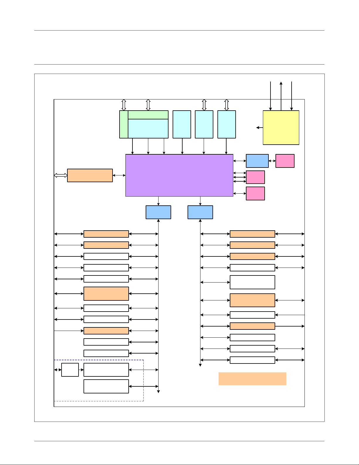
AHB to
APB bridge
AHB to
APB bridge
APB slave group 1APB slave group 0
Note: shaded peripheral blocks
support General Purpose DMA
RTC Power Domain
Multilayer AHB Matrix
I2C2
I2S
UARTs 2 & 3
SSP0
Real Time Clock
20 bytes of backup
registers
SSP1
UARTs 0 & 1
CAN 1 & 2
I2C 0 & 1
SPI0
Capture/Compare
Timers 0 & 1
Watchdog Timer
PWM1
12-bit ADC
Pin Connect Block
GPIO Interrupt Ctl
32 kHz
oscillator
DMA
controller
Clock Generation,
Power Control,
Brownout Detect,
and other
system functions
RST
Xtalin
Xtalout
Clocks
and
Controls
Ethernet
PHY
interface
Ethernet
10/100
MAC
USB
device,
host,
OTG
USB
interface
JTAG
interface
ARM Cortex-M3
Test/Debug Interface
System
bus
D-code
bus
I-code
bus
ROM
8 kB
SRAM
64 kB
Trace
Port
Trace Module
High Speed GPIO
Capture/Compare
Timers 2 & 3
External Interrupts
DAC
System Control
Motor Control PWM
Quadrature Encoder
Repetitive Interrupt
Timer
Flash
512 kB
Flash
Accelerator
1.5 Simplified block diagram
UM10360
Chapter 1: LPC17xx Introductory information
Fig 1. LPC1768 simplified block diagram
UM10360 All information provided in this document is subject to legal disclaimers. © NXP B.V. 2010. All rights reserved.
User manual Rev. 2 — 19 August 2010 8 of 840
Page 9

NXP Semiconductors
1.6 Architectural overview
The ARM Cortex-M3 includes three AHB-Lite buses, one system bus and the I-code and
D-code buses which are faster and are used similarly to TCM interfaces: one bus
dedicated for instruction fetch (I-code) and one bus for data access (D-code). The use of
two core buses allows for simultaneous operations if concurrent ope rations target dif ferent
devices.
The LPC17xx uses a multi-layer AHB matrix to connect the Cortex-M3 buses and other
bus masters to peripherals in a flexible manner that optimizes performance by allowing
peripherals on different slaves ports of the matrix to be accessed simultaneously by
different bus masters. Det ails of the multilayer matrix connections are shown in Figure 2
APB peripherals are connected to the CPU via two APB busses using separate slave
ports from the multilayer AHB matrix. This allows for better performance by reducing
collisions between the CPU and the DMA controller. The APB bus bridges are configured
to buffer writes so that the CPU or DMA controller can write to APB devices without
always waiting for APB write completion.
UM10360
Chapter 1: LPC17xx Introductory information
.
1.7 ARM Cortex-M3 processor
The ARM Cortex-M3 is a general purpose 32-bit microprocessor, which offers high
performance and very low power consumption. The Cortex-M3 offers many new features,
including a Thumb-2 instruction set, low interrupt latency, hardware divide,
interruptible/continuable multiple load and store instructions, automatic state save and
restore for interrupts, tightly integrated interrupt controller with Wakeup Interrupt
Controller, and multiple core buses capable of simultaneous accesses.
Pipeline techniques are employed so that all pa rts of the p rocessing and memory systems
can operate continuously. T ypically, while one instruction is being executed, its successor
is being decoded, and a third instruction is being fetched from memory.
The ARM Cortex-M3 processor is described in detail in the Cortex-M3 User Guide that is
appended to this manual.
1.7.1 Cortex-M3 Configuration Options
The LPC17xx uses the r2p0 version of the Cortex-M3 CPU, which includes a number of
configurable options, as noted below.
System options:
• The Nested Vectored Inter rupt Controller (NVIC) is included. The NVIC includes the
SYSTICK timer.
• The Wakeup Interrupt Controller (WIC) is included. The WIC allows more powerful
options for waking up the CPU from reduced power modes.
• A Memory Protection Unit (MPU) is included.
• A ROM Table in included. The ROM Table provides addresses of debug components
to external debug systems.
UM10360 All information provided in this document is subject to legal disclaimers. © NXP B.V. 2010. All rights reserved.
User manual Rev. 2 — 19 August 2010 9 of 840
Page 10

NXP Semiconductors
Debug related options:
• A JTAG debug interface is included.
• Serial Wire Debug is included. Serial Wire Debug allows debug op erations u sing only
• The Embedded Trace Macrocell (ETM) is included. The ETM provides instruction
• The Data Watchpoint and Trace (DWT) unit is included. The DWT allows data
• An Instrumentation T race Macrocell (ITM) is included. Software can write to the ITM in
• The Trace Port Interface Unit (TPIU) is included. The TPIU encodes and provides
• A Flash Patch and Breakpoint (FPB) is included. The FPB can generate hardware
UM10360
Chapter 1: LPC17xx Introductory information
2 wires, simple trace functions can be added with a third wire.
trace capabilities.
address or data value matches to be trace information or trigger other events. The
DWT includes 4 comparators and counters for certain internal events.
order to send messages to the trace port.
trace information to the outside world. This can be on the Serial Wire V iewer pin or the
4-bit parallel trace port.
breakpoints and remap specific addresses in code space to SRAM as a temporary
method of altering non-volatile code. The FPB include 2 literal comparators and 6
instruction comparators.
1.8 On-chip flash memory system
The LPC17xx contains up to 512 kB of on-chip flash memory. A flash memory accelerator
maximizes performance for use with the two fast AHB-Lite buses. This memory may be
used for both code and data storage. Programming of the flash memory may be
accomplished in several ways. It may be programmed In System via the serial port. The
application program may also erase and/or program the flash while the application is
running, allowing a great degree of flexibility for data storage field firmware upgrades, etc.
1.9 On-chip Static RAM
The LPC17xx contains up to 64 kB of on-chip static RAM memory. Up to 32 kB of SRAM,
accessible by the CPU and all three DMA controllers are on a higher-speed bus. Devices
containing more than 32 kB SRAM have two additional 16 kB SRAM blocks, each situated
on separate slave ports on the AHB multilayer matrix.
This architecture allows the possibility for CPU and DMA accesses to be separated in
such a way that there are few or no delays for the bus masters.
UM10360 All information provided in this document is subject to legal disclaimers. © NXP B.V. 2010. All rights reserved.
User manual Rev. 2 — 19 August 2010 10 of 840
Page 11
NXP Semiconductors
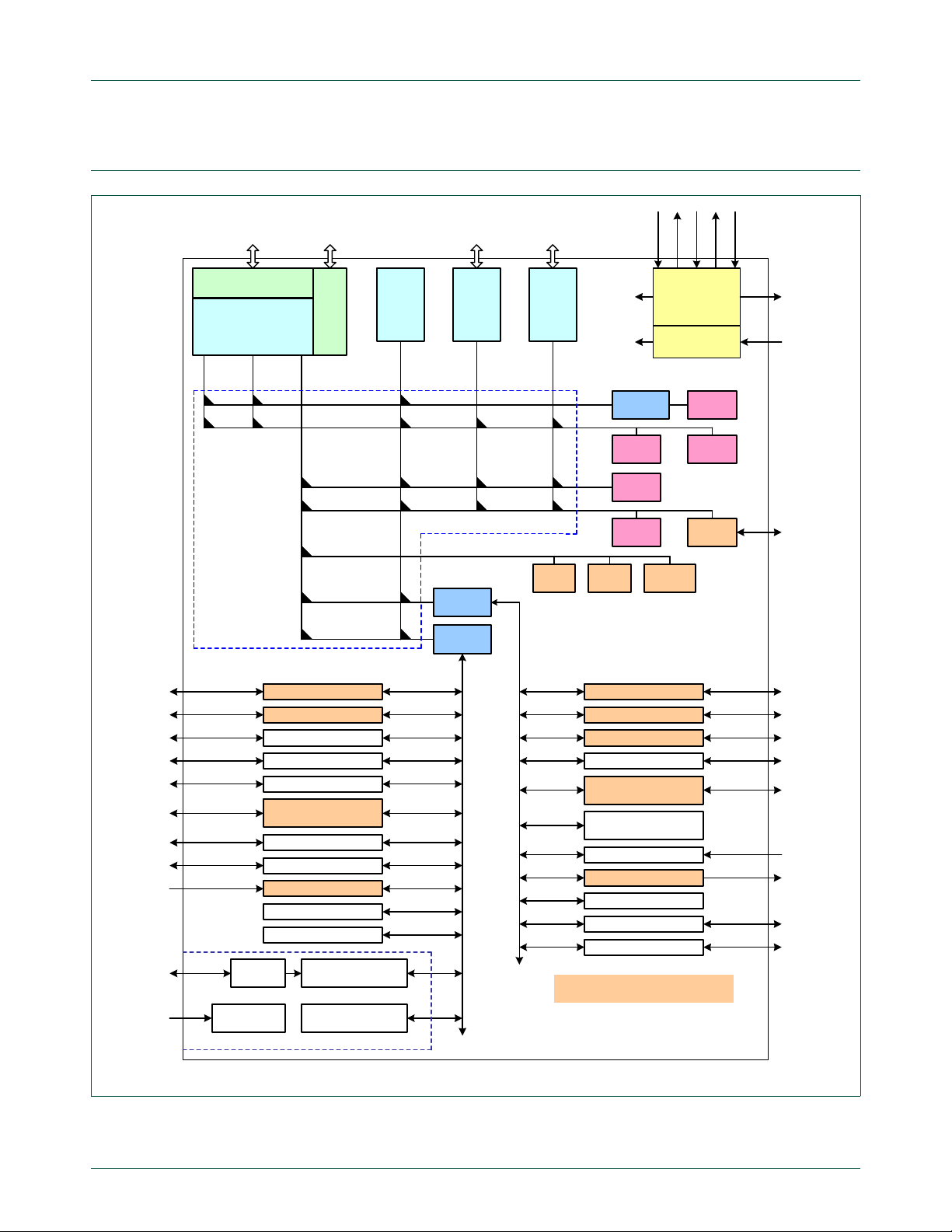
Multilayer
AHB Matrix
AHB to
APB bridge
AHB to
APB bridge
JTAG
interface Debug Port
Ethernet PHY
interface
SRAM
16 kB
SRAM
16 kB
EMULATION
TRACE MODULE
ARM Cortex-M3
TEST/DEBUG
INTERFACE
USB
device,
host,
OTG
USB
interface
DMA
controller
Ethernet
10/100
MAC
System
bus
D-code
bus
I-code
bus
DMAC
regs
USB
regs
Ethernet
regs
clock generation,
power control,
and other
system functions
SRAM
32 kB
ROM
8 kB
Flash
512 kB
Flash
Accelerator
RST
Xtalin
Xtalout
X32Kin
X32Kout
APB slave group 1
Note: shaded peripheral blocks
support General Purpose DMA
Capture/compare
timers 2 & 3
I2C2
I2S
UARTs 2 & 3
SSP0
External interrupts
DAC
System control
Motor control PWM
Quadrature encoder
APB slave group 0
RTC Power Domain
Real Time Clock
SSP1
UARTs 0 & 1
CAN 1 & 2
I2C 0 & 1
SPI0
Capture/compare
timers 0 & 1
Watchdog timer
PWM1
12-bit ADC
Pin connect block
GPIO interrupt control
32 kHz
oscillator
Backup registers
(20 bytes)
Repetitive interrupt
timer
ultra-low power
regulator
Vbat
voltage regulator
clocks
and
controls
internal
power
Vdd
CLK
OUT
HS
GPIO
1.10 Block diagram
UM10360
Chapter 1: LPC17xx Introductory information
UM10360 All information provided in this document is subject to legal disclaimers. © NXP B.V. 2010. All rights reserved.
User manual Rev. 2 — 19 August 2010 11 of 840
Fig 2. LPC1768 block diagram, CPU and buses
Page 12

UM10360
Chapter 2: LPC17xx Memory map
Rev. 2 — 19 August 2010 User manual
2.1 Memory map and peripheral addressing
The ARM Cortex-M3 processor has a single 4 GB address space. The following table
shows how this space is used on the LPC17xx.
Table 3. LPC17xx memory usage and details
Address range General Use Address range details and description
0x0000 0000 to
0x1FFF FFFF
0x2000 0000 to
0x3FFF FFFF
0x4000 0000 to
0x5FFF FFFF
0xE000 0000 to
0xE00F FFFF
On-chip non-volatile
memory
On-chip SRAM 0x1000 0000 - 0x1000 7FFF For devices with 32 kB of local SRAM.
Boot ROM 0x1FFF 0000 - 0x1FFF 1FFF 8 kB Boot ROM with flash services.
On-chip SRAM
(typically used for
peripheral data)
GPIO 0x2009 C000 - 0x2009 FFFF GPIO.
APB Peripherals 0x4000 0000 - 0x4007 FFFF APB0 Peripherals, up to 32 peripheral blocks,
AHB peripherals 0x5000 0000 - 0x501F FFFF DMA Controller, Ethernet interface, and USB
Cortex-M3 Private
Peripheral Bus
0x0000 0000 - 0x0007 FFFF For devices with 512 kB of flash memory.
0x0000 0000 - 0x0003 FFFF For devices with 256 kB of flash memory.
0x0000 0000 - 0x0001 FFFF For devices with 128 kB of flash memory.
0x0000 0000 - 0x0000 FFFF For devices with 64 kB of flash memory.
0x0000 0000 - 0x0000 7FFF For devices with 32 kB of flash memory.
0x1000 0000 - 0x1000 3FFF For devices with 16 kB of local SRAM.
0x1000 0000 - 0x1000 1FFF For devices with 8 kB of local SRAM.
0x2007 C000 - 0x2007 FFFF AHB SRAM - bank 0 (16 kB), present on
devices with 32 kB or 64 kB of total SRAM.
0x2008 0000 - 0x2008 3FFF AHB SRAM - bank 1 (16 kB), present on
devices with 64 kB of total SRAM.
16 kB each.
0x4008 0000 - 0x400F FFFF APB1 Peripherals, up to 32 peripheral blocks,
16 kB each.
interface.
0xE000 0000 - 0xE00F FFFF Cortex-M3 related functions, includes the
NVIC and System Tick Timer.
2.2 Memory maps
The LPC17xx incorporates several distinct memory regions, shown in the following
figures. Figure 3
program viewpoint following reset. The interrupt vector area supports address remapping,
which is described later in this section.
UM10360 All information provided in this document is subject to legal disclaimers. © NXP B.V. 2010. All rights reserved.
User manual Rev. 2 — 19 August 2010 12 of 840
shows the overall map of the entire address space from the user
Page 13
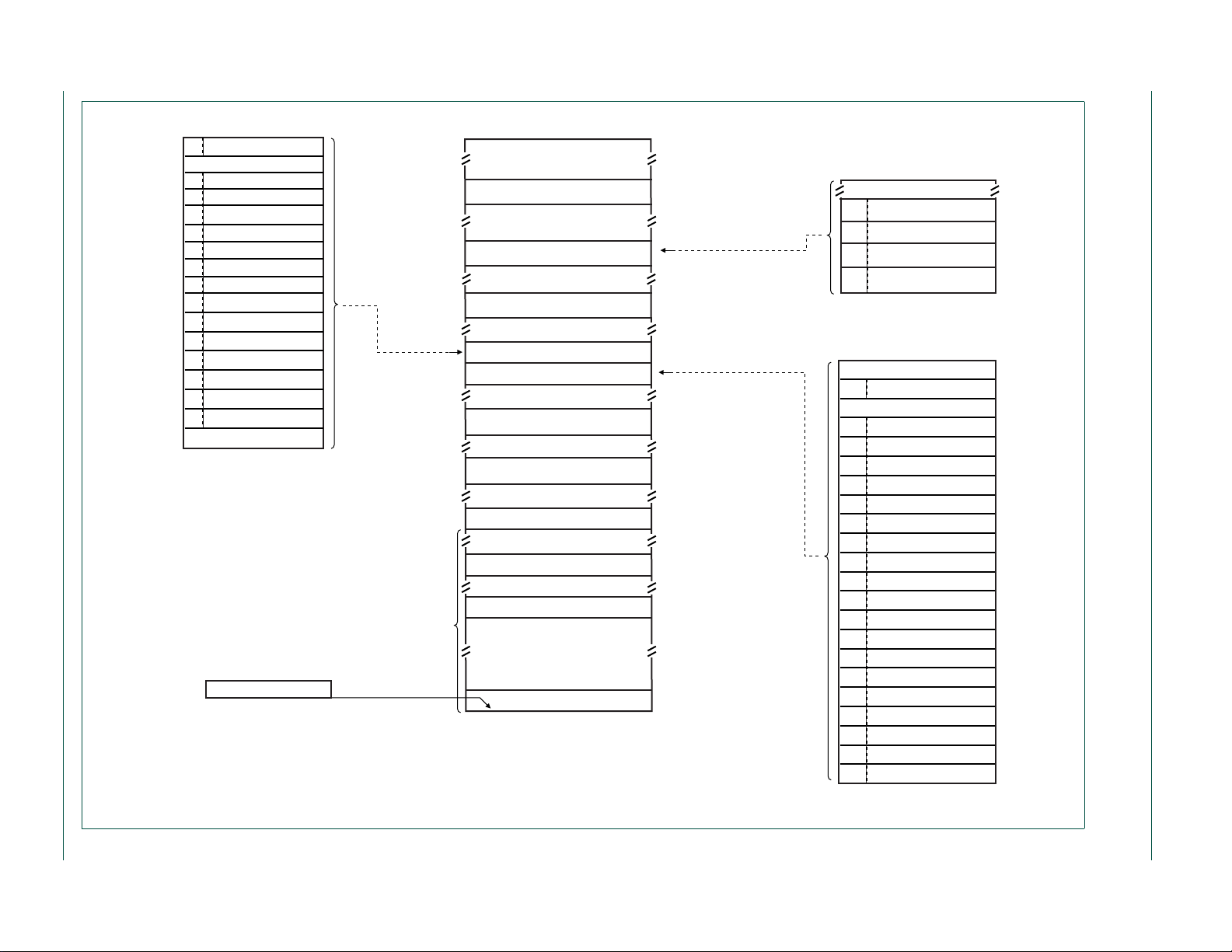
User manual Rev. 2 — 19 August 2010 13 of 840
0x5000 0000
0x5000 4000
0x5000 8000
0x5000 C000
0x5020 0000
AHB peripherals
Ethernet controller
USB controller
reserved
127- 4 reserved
GPDMA controller
0
1
2
3
APB0 peripherals
0x4000 4000
0x4000 8000
0x4000 C000
0x4001 0000
0x4001 8000
0x4002 0000
0x4002 8000
0x4002 C000
0x4003 4000
0x4003 0000
0x4003 8000
0x4003 C000
0x4004 0000
0x4004 4000
0x4004 8000
0x4004 C000
0x4005 C000
0x4006 0000
0x4008 0000
0x4002 4000
0x4001 C000
0x4001 4000
0x4000 0000
WDT
TIMER0
TIMER1
UART0
UART1
reserved
I2C0
SPI
RTC + backup registers
GPIO interrupts
pin connect
SSP1
ADC
CAN AF RAM
CAN AF registers
CAN common
CAN1
CAN2
22 - 19 reserved
I2C1
31 - 24 reserved
0
1
2
3
4
5
6
7
8
9
10
11
12
13
14
15
16
17
18
23
APB1 peripherals
0x4008 0000
0x4008 8000
0x4008 C000
0x4009 0000
0x4009 4000
0x4009 8000
0x4009 C000
0x400A 0000
0x400A 4000
0x400A 8000
0x400A C000
0x400B 0000
0x400B 4000
0x400B 8000
0x400B C000
0x400C 0000
0x400F C000
0x4010 0000
SSP0
DAC
Timer 2
Timer 3
UART2
UART3
reserved
I2S
I2C2
1 - 0 reserved
2
3
4
5
6
7
8
9
10
reserved
repetitive interrupt timer
11
12
reserved
motor control PWM
30 - 16 reserved
13
14
15
system control31
reserved
reserved
32 kB local static RAM
reserved
reserved
private peripheral bus
0x0000 0000
0 GB
0.5 GB
4 GB
1 GB
0x0008 0000
0x1000 0000
0x1000 8000
0x1FFF 0000
0x1FFF 2000
0x2007 C000
0x2008 4000
0x2009 C000
0x200A 0000
0x2200 0000
0x2400 0000
0x4000 0000
0x4008 0000
0x4010 0000
0x4200 0000
0x4400 0000
0x5000 0000
0x5020 0000
0xE000 0000
0xE010 0000
0xFFFF FFFF
reserved
reserved
GPIO
reserved
reserved
reserved
reserved
APB0 peripherals
AHB periherals
APB1 peripherals
AHB SRAM bit band alias addressing
peripheral bit band alias addressing
AHB SRAM (2 blocks of 16 kB)
LPC1768 memory space
512 kB on-chip flash
QEI
PWM1
8 kB boot ROM
0x0000 0000
0x0000 0400
active interrupt vectors
+ 256 words
I-code/D-code
memory space
xxxxxxxxxxxxxxxxxxxxx xxxxxxxxxxxxxxxxxxxxxxxxxx xxxxxxx x x x xxxxxxxxxxxxxxxxxxxxxxxxxxxxxx xxxxxxxxxxxxxxxxxxx xx xx xxxxx
xxxxxxxxxxxxxxxxxxxxxxxxxxx xxxxxxxxxxxxxxxxxxx xxxxxx xxxxxxxxxxxxxxxxxxxxxxxxxxxxxxxxxxx xxxxxxxxxxxx x x
xxxxxxxxxxxxxxxxxxxxx xxxxxxxxxxxxxxxxxxxxxxxxxxxxxx xxxxx xxxxxxxxxxxxxxxxxxxxxxxxxxxxxxxxxxxxxxxxxxxxxxxxxx xxxxxxxx
UM10360 All information provided in this document is subject to legal disclaimers. © NXP B.V. 2010. All rights reserved.
xxxxxxxxxxxxxxxxxxxxxxxxx xxxxxxxxxxxxxxxxxxxx xxx
NXP Semiconductors
Fig 3. LPC17xx system memory map
Chapter 2: LPC17xx Memory map
UM10360
Page 14

NXP Semiconductors
Figure 3 and Table 4 show different views of the peripheral address space. The AHB
peripheral area is 2 megabyte in size, and is divided to allow for up to 128 peripherals.
The APB peripheral area is 1 megabyte in size and is divided to allow for up to 64
peripherals. Each peripheral of either type is allocated 16 kilobytes of space. This allows
simplifying the address decoding for each peripheral.
All peripheral register addresses are word aligned (to 32-bit boundaries) regardless of
their size. This eliminates the need for byte lane mapping hardware that would be required
to allow byte (8-bit) or half-word (16-bit) accesses to occur at smaller boundaries. An
implication of this is that word and half-word registers must be accessed all at once. For
example, it is not possible to read or write the upper byte of a word register separately.
2.3 APB peripheral addresses
The following table shows the APB0/1 address maps. No APB peripheral uses all of the
16 kB space allocated to it. Typically each device’s registers are "aliased" or repeated at
multiple locations within each 16 kB range.
T able 4. APB0 peripherals and base addresses
APB0 peripheral Base address Peripheral name
0 0x4000 0000 Watchdog Timer
1 0x4000 4000 Timer 0
2 0x4000 8000 Timer 1
3 0x4000 C000 UART0
4 0x4001 0000 UART1
5 0x4001 4000 reserved
6 0x4001 8000 PWM1
7 0x4001 C000 I
8 0x4002 0000 SPI
9 0x4002 4000 RTC
10 0x4002 8000 GPIO interrupts
11 0x4002 C000 Pin Connect Block
12 0x4003 0000 SSP1
13 0x4003 4000 ADC
14 0x4003 8000 CAN Acceptance Filter RAM
15 0x4003 C000 CAN Acceptance Filter Registers
16 0x4004 0000 CAN Common Registers
17 0x4004 4000 CAN Controller 1
18 0x4004 8000 CAN Controller 2
19 to 22 0x4004 C000 to 0x4005 8000 reserved
23 0x4005 C000 I
24 to 31 0x4006 0000 to 0x4007 C000 reserved
UM10360
Chapter 2: LPC17xx Memory map
2
C0
2
C1
UM10360 All information provided in this document is subject to legal disclaimers. © NXP B.V. 2010. All rights reserved.
User manual Rev. 2 — 19 August 2010 14 of 840
Page 15

NXP Semiconductors
T able 5. APB1 peripherals and base addresses
APB1 peripheral Base address Peripheral name
0 0x4008 0000 reserved
1 0x4008 4000 reserved
2 0x4008 8000 SSP0
3 0x4008 C000 DAC
4 0x4009 0000 Timer 2
5 0x4009 4000 Timer 3
6 0x4009 8000 UART2
7 0x4009 C000 UART3
8 0x400A 0000 I
9 0x400A 4000 reserved
10 0x400A 8000 I
11 0x400A C000 reserved
12 0x400B 0000 Repetit ive interrupt timer
13 0x400B 4000 reserved
14 0x400B 8000 Motor control PWM
15 0x400B C000 Quadrature Encoder Interface
16 to 30 0x400C 0000 to 0x400F 8000 reserved
31 0x400F C000 System control
UM10360
Chapter 2: LPC17xx Memory map
2
C2
2
S
2.4 Memory re-mapping
The Cortex-M3 incorporates a mechanism that allows remapping the interrupt vector table
to alternate locations in the memory map. This is controlled via the Vector Table Offset
Register contained in the Cortex-M3. Refer to Section 6.4
and Section 34.4.3.5 of the
Cortex-M3 User Guide appended to this manual for details of the Vector Table Offset
feature.
Boot ROM re-mapping
Following a hardware reset, the Boot ROM is temporarily mapped to address 0. This is
normally transparent to the user . However , if execution is halted imm ediately after reset by
a debugger, it should correct the mapping for the user. See Section 33.6
.
2.5 AHB arbitration
The Multilayer AHB Matrix arbitrates between several masters. By default, the Cortex-M3
D-code bus has the highest priority, followed by the I-Code bus. All other masters share a
lower priority.
2.6 Bus fault exceptions
The LPC17xx generates Bus Fault exception if an access is a ttempted for an add ress that
is in a reserved or unassigned address region. The regions are are as of the memor y map
that are not implemented for a specific derivative. These include all spaces marked
“reserved” in Figure 3
UM10360 All information provided in this document is subject to legal disclaimers. © NXP B.V. 2010. All rights reserved.
User manual Rev. 2 — 19 August 2010 15 of 840
.
Page 16

NXP Semiconductors
For these areas, both attempted data acce ss and in struction fetch genera te an exception.
In addition, a Bus Fault exception is generated for any instruction fetch that maps to an
AHB or APB peripheral address.
Within the address space of an existing APB peripheral, an exception is not generated in
response to an access to an undefined address. Address decoding within e ach peripheral
is limited to that needed to distinguish defined registers within the peripheral itself. For
example, an access to address 0x4000 D000 (an undefined address within the UART0
space) may result in an access to the register defined at address 0x4000C000. Details of
such address aliasing within a peripheral space are not defined in the LPC17xx
documentation and are not a supported feature.
If software executes a write directly to the flash memory, the flash accelerator will
generate a Bus Fault exception. Flash prog r amm i ng must be acco m plis he d by using the
specified flash programming interface provided by the Boot Code.
Note that the Cortex-M3 core stores the exception flag along with the associated
instruction in the pipeline and processes the exception only if an attempt is made to
execute the instruction fetched from the disallowed address. This prevents accidental
aborts that could be caused by prefetches that occur when code is executed very near a
memory boundary.
UM10360
Chapter 2: LPC17xx Memory map
UM10360 All information provided in this document is subject to legal disclaimers. © NXP B.V. 2010. All rights reserved.
User manual Rev. 2 — 19 August 2010 16 of 840
Page 17

3.1 Introduction
UM10360
Chapter 3: LPC17xx System control
Rev. 2 — 19 August 2010 User manual
The system control block includes several system features and control registers for a
number of functions that are not related to specific peripheral devices. These include:
• Reset
• Brown-Out Detection
• External Interrupt Input s
• Miscellaneous System Controls and Status
Each type of function has its own register(s) if any are required and unneeded bits are
defined as reserved in order to allow future expansion. Unrelated functions never share
the same register addresses
3.2 Pin description
Table 6 shows pins tha t ar e as soc i at ed with Syst em Con tr ol block fu nctions.
Table 6. Pin summary
Pin name Pin
EINT0 Input External Interrupt In put 0 - An active low/high level or falling/rising
EINT1 Input
EINT2 Input
EINT3 Input
RESET
Pin description
direction
edge general purpose interrupt input. This pin may be used to wake up
the processor from Sleep, Deep-sleep, or Power-down modes.
External Interrupt Input 1 - See the EINT0 description above.
External Interrupt Input 2 - See the EINT0 description above.
External Interrupt Input 3 - See the EINT0 description above.
Input External Reset input - A LOW on this pin resets the chip, causing I/O
ports and peripherals to take on their default states, and the processor to
begin execution at address 0x0000 0000.
UM10360 All information provided in this document is subject to legal disclaimers. © NXP B.V. 2010. All rights reserved.
User manual Rev. 2 — 19 August 2010 17 of 840
Page 18

NXP Semiconductors
3.3 Register description
All registers, regardless of size, are on word address boundaries. Details of the registers
appear in the description of each function.
T able 7. Summary of system control registers
Name Description Access Reset value Address
External Interrupts
EXTINT External Interrup t Flag Register R/W 0 0x400F C140
EXTMODE External Interrupt Mode register R/W 0 0x400F C148
EXTPOLAR External Interrupt Polarity Register R/W 0 0x 400F C14C
Reset
RSID Reset Source Iden tif icatio n Register R/W see Table 8 0x400F C180
Syscon Miscellaneous Registers
SCS System Control and Status R/W 0 0x400F C1A0
3.4 Reset
UM10360
Chapter 3: LPC17xx System control
Reset has 4 sources on the LPC17xx: the RESET pin, Watchdog Reset, Power On Reset
(POR), and Brown Out Detect (BOD).
The RESET
pin is a Schmitt trigger input pin. Assertion of chip Reset by any source, once
the operating voltage attains a usable level, starts the wake-up timer (see description in
Section 4.9 “
Wake-up timer” in this chapter), causing reset to remain asserted until the
external Reset is de-asserted, the oscillator is running, a fixed number of clocks have
passed, and the flash controller has completed it s initialization. The reset logic is shown in
the following block diagram (see Figure 4
).
UM10360 All information provided in this document is subject to legal disclaimers. © NXP B.V. 2010. All rights reserved.
User manual Rev. 2 — 19 August 2010 18 of 840
Page 19
NXP Semiconductors
C
Q
S
APB read of
PDBIT
in PCON
power-down
C
Q
S
F
OSC
to other
blocks
WAKE-UP TIMER
watchdog
reset
external
reset
START
COUNT 2
n
internal RC
oscillator
Reset to the
on-chip circuitry
Reset to
PCON.PD
write “1”
from APB
reset
EINT0 wake-up
EINT1 wake-up
EINT2 wake-up
POR
BOD
EINT3 wake-up
RTC wake-up
BOD wake-up
Ethernet MAC wake-up
USB need_clk wake-up
CAN wake-up
GPIO0 port wake-up
GPIO2 port wake-up
UM10360
Chapter 3: LPC17xx System control
Fig 4. Reset block diagram including the wake-up timer
UM10360 All information provided in this document is subject to legal disclaimers. © NXP B.V. 2010. All rights reserved.
User manual Rev. 2 — 19 August 2010 19 of 840
On the assertion of a reset source external to the Cortex-M3 CPU (POR, BOD reset,
External reset, and Watchdog reset), the IRC starts up. After the IRC-start-up time
(maximum of 60 μs on power-up) and after the IRC provides a stable clock output, the
reset signal is latched and synchronized on the IRC clock. Then the following two
sequences start simultaneously:
1. The 2-bit IRC wake-up timer starts counting when the synchronized reset is
de-asserted. The boot code in the ROM starts when the 2-bit IRC wake-up timer times
out. The boot code performs the boot tasks and may jump to the flash. If the flash is
not ready to access, the Flash Accelerator will insert wait cycles until the flash is
ready.
2. The flash wake-up timer (9-bit) starts counting when the synchronized reset is
de-asserted. The flash wakeup-timer generates the 100 μs flash start-up time. Once it
times out, the flash initialization sequence is started, which takes about 250 cycles.
When it’s done, the Flash Accelerator will be granted access to the flash.
When the internal Reset is removed, the processor begins executing at address 0, which
is initially the Reset vector mapped from the Boot Block. At that point, all of the processor
and peripheral registers have been initialized to predetermined values.
Figure 5
shows an example of the relationship between the RESET, the IRC, and the
processor status when the LPC17xx starts up after reset. See Section 4.3.2 “
oscillator” for start-up of the main oscillator if selected by the user code.
Main
Page 20
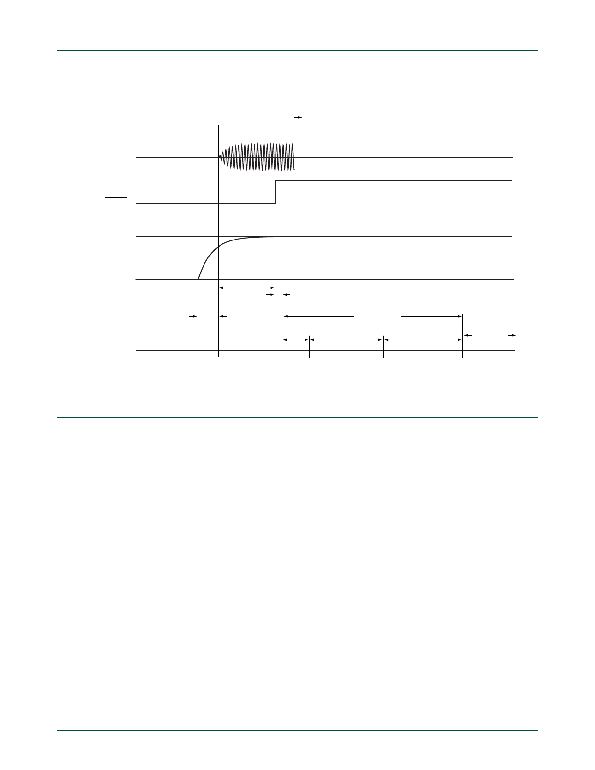
NXP Semiconductors
valid threshold
processor status
V
DD(REG)(3V3)
IRC status
RESET
GND
60 μs
1 μs; IRC stability count
boot time
user code
boot code
execution
finishes;
user code starts
flash read
starts
flash read
finishes
IRC
starts
IRC
stable
supply ramp-up
time
7 μs 181 μs 224 μs
UM10360
Chapter 3: LPC17xx System control
Fig 5. Example of start-up after reset
UM10360 All information provided in this document is subject to legal disclaimers. © NXP B.V. 2010. All rights reserved.
User manual Rev. 2 — 19 August 2010 20 of 840
Page 21

NXP Semiconductors
3.4.1 Reset Source Identification Register (RSID - 0x400F C180)
This register contains one bit for each source of Reset. Writing a 1 to any of these bits
clears the corresponding read-side bit to 0. The interactions among the four sources are
described below.
Table 8. Reset Source Identification register (RSID - address 0x400F C180) bit description
Bit Symbol Description Reset
0 POR Assertion of the POR signal sets this bit, and clears all of the other bits in
1 EXTR Assertion of the RESET
2 WDTR This bit is set when the Watchdog Timer times out and the WDTRESET bit
3 BODR This bit is set when the V
31:4 - Reserved, user software should not write ones to reserved bits. The value
UM10360
Chapter 3: LPC17xx System control
this register. But if another Reset signal (e.g., External Reset) remains
asserted after the POR signal is negated, then its bit is set. This bit is not
affected by any of the other sources of Reset.
signal sets this bit. This bit is cleared only by
software or POR.
in the Watchdog Mode Register is 1. This bit is cleared only by software or
POR.
BOD reset trip level (typically 1.85 V under nominal room temperature
DD(REG)(3V3)
conditions).
If the V
DD(REG)(3V3)
voltage dips from the normal operating range to below
the BOD reset trip level and recovers, the BODR bit will be set to 1.
If the V
DD(REG)(3V3)
voltage dips from the normal operating range to below
the BOD reset trip level and continues to decline to the level at which POR
is asserted (nominally 1 V), the BODR bit is cleared.
If the V
DD(REG)(3V3)
voltage rises continuously from below 1 V to a level
above the BOD reset trip level, the BODR will be set to 1.
This bit is cleared only by software or POR.
Note: Only in the case where a reset occurs and the POR = 0, the BODR
bit indicates if the V
DD(REG)(3V3)
or not.
read from a reserved bit is not defined.
voltage reaches a level below the
voltage was below the BOD reset trip level
value
See
text
See
text
See
text
See
text
NA
UM10360 All information provided in this document is subject to legal disclaimers. © NXP B.V. 2010. All rights reserved.
User manual Rev. 2 — 19 August 2010 21 of 840
Page 22

NXP Semiconductors
3.5 Brown-out detection
The LPC17xx includes a Brown-Out Detector (BOD) that provides 2-stage monitoring of
the voltage on the V
(typically 2.2 V under nominal room temperature conditions), the BOD asserts an interrupt
signal to the NVIC. This signal can be enabled for interrupt in the Interrupt Enable
Register in the NVIC in order to cause a CPU interrupt; if not, software can monitor the
signal by reading the Raw Interrupt Status Register.
The second stage of low-voltage d etection a sse rts Reset to inactivate the LPC17xx when
the voltage on the V
under nominal room temperature cond itio ns ). T his Rese t pre ve nts altera tio n of th e flas h
as operation of the various elements of the chip would otherwise become unreliable due
to low voltage. The BOD circuit maintains this reset down below 1 V, at which point the
Power-On Reset circuitry maintains the overall Reset.
Both the BOD reset interrupt level and the BOD reset trip level thresholds include some
hysteresis. In normal operation, this hysteresis allows the BOD reset interrupt level
detection to reliably interrupt, or a regularly-executed event loop to sense the condition.
DD(REG)(3V3)
DD(REG)(3V3)
UM10360
Chapter 3: LPC17xx System control
pins. If this voltage falls below the BOD interrupt trip level
pins falls below the BOD reset trip level (typically 1.85 V
But when Brown-Out Detection is enabled to bring the LPC17xx out of Power-down mode
(which is itself not a guaranteed operation -- see Section 4.8.7 “
register (PCON - 0x400F C0C0)”), the supply voltage may re cover from a transient b efore
the wake-up timer has completed its delay. In this case, the net result of the transient BOD
is that the part wakes up and continues operation after the instructions that set
Power-down mode, without any interrupt occurring and with the BOD bit in the RSID being
0. Since all other wake-up conditions have latching flags (see Section 3.6.2 “
Interrupt flag register (EXTINT - 0x400F C140)” and Section 27.6.2), a wake-up of this
type, without any apparent cause, can be assumed to be a Brown-Out that has gone
away.
Power Mode Control
External
UM10360 All information provided in this document is subject to legal disclaimers. © NXP B.V. 2010. All rights reserved.
User manual Rev. 2 — 19 August 2010 22 of 840
Page 23
NXP Semiconductors
Interrupt flag
(one bit of EXTINT)
write to EXTINTi
internal reset
EINTi to wakeup timer
EINTi pin
EXTMODEi
PCLK
to interrupt
controller
EXTPOLARi
EINTi interrupt enable
PCLK
1
GLITCH
FILTER
APB read
of EXTINTi
Q
S
R
Q
S
R
Q
S
D
100621
3.6 External interrupt inputs
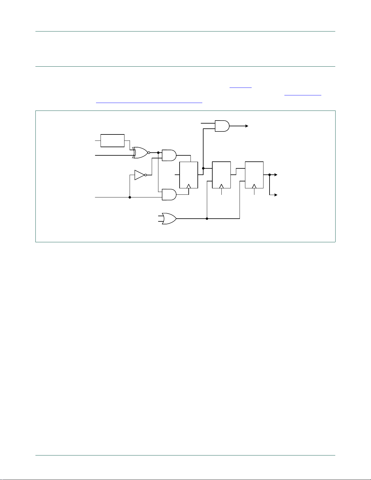
TheLPC17xx includes four External Interrupt Inputs as selectable pin functions. The logic
of an individual external interrupt is r epresented in Figure 6
have the ability to wake up the CPU from Power-down mode. Refer to Section 4.8.8
“Wake-up from Reduced Power Modes” for details.
UM10360
Chapter 3: LPC17xx System control
. In addition, external interrupts
Fig 6. External interrupt logic
UM10360 All information provided in this document is subject to legal disclaimers. © NXP B.V. 2010. All rights reserved.
User manual Rev. 2 — 19 August 2010 23 of 840
Page 24

NXP Semiconductors
3.6.1 Register description
The external interrupt function has four registers associated with it. The EXTINT register
contains the interrupt flags. The EXTMODE and EXTPOLAR registers specify the level
and edge sensitivity parameters.
Table 9. External Interrupt registers
Name Description Access Reset
EXTINT The External Interrupt Flag Register contains
EXTMODE The External Interrupt Mode Register controls
EXTPOLAR The External Interrupt Polarity Register controls
[1] Reset Value reflects the data stored in used bits only. It does not include reserved bits content.
Chapter 3: LPC17xx System control
interrupt flags for EINT0, EINT1, EINT2 and
EINT3. See Table 10
whether each pin is edge- or level-sensitive.
See Table 11
which level or edge on each pin will cause an
interrupt. See Table 12
.
.
.
UM10360
Address
[1]
value
R/W 0x00 0x400F C140
R/W 0x00 0x400F C148
R/W 0x00 0x400F C14C
3.6.2 External Interrupt flag register (EXTINT - 0x400F C140)
When a pin is selected for its external interrupt function, the level or edge on that pin
(selected by its bits in the EXTPOLAR a nd EXTMODE registers) will set its interrup t flag in
this register. This asserts the corresponding interrupt request to the NVIC, which will
cause an interrupt if interrupts from the pin are enabled.
Writing ones to bits EINT0 through EINT3 in EXTINT register clears the corresponding
bits. In level-sensitive mode the interrupt is cleared only when the pin is in its inactive
state.
Once a bit from EINT0 to EINT3 is set and an appropriate code st arts to execute (hand ling
wake-up and/or external interrupt), this bit in EXTINT register must be cleared. Otherwise
event that was just triggered by activity on the EINT pin will not be recognized in future.
Important: whenever a change of external interrupt operating mode (i.e. active
level/edge) is performed (including the initialization of an external interrupt), the
corresponding bit in the EXTINT register must be cleared! For details see
Section 3.6.3 “
Section 3.6.4 “
For example, if a system wakes up from Power-down using low level on external interrupt
0 pin, its post wake-up code must reset EINT0 bit in order to allow future entry into the
Power-down mode. If EINT0 bit is left set to 1, subsequent attempt(s) to invoke
Power-down mode will fail. The same goes for external interrupt handling.
External Interrupt Mode register (EXTMODE - 0x400F C148)” and
External Interrupt Polarity register (EXTPOLAR - 0x400F C14C)”.
More details on Power-down mode will be discussed in the following chapters.
UM10360 All information provided in this document is subject to legal disclaimers. © NXP B.V. 2010. All rights reserved.
User manual Rev. 2 — 19 August 2010 24 of 840
Page 25

NXP Semiconductors
Table 10. External Interrupt Flag reg ister (EXTINT - address 0x400F C140) bit description
Bit Symbol Description Reset
0 EINT0 In level-sensitive mode, this bit is set if the EINT0 function is selected for
1 EINT1 In level-sensitive mode, this bit is set if the EINT1 function is selected for
2 EINT2 In level-sensitive mode, this bit is set if the EINT2 function is selected for
3 EINT3 In level-sensitive mode, this bit is set if the EINT3 function is selected for
31:4 - Reserved, user software should not write ones to reserved bits. The value
UM10360
Chapter 3: LPC17xx System control
its pin, and the pin is in its active state. In edge-sensitive mode, this bit is
set if the EINT0 function is selected for its pin, and the selected edge
occurs on the pin.
This bit is cleared by writing a one to it, except in level sensitive mode
when the pin is in its active state.
its pin, and the pin is in its active state. In edge-sensitive mode, this bit is
set if the EINT1 function is selected for its pin, and the selected edge
occurs on the pin.
This bit is cleared by writing a one to it, except in level sensitive mode
when the pin is in its active state.
its pin, and the pin is in its active state. In edge-sensitive mode, this bit is
set if the EINT2 function is selected for its pin, and the selected edge
occurs on the pin.
This bit is cleared by writing a one to it, except in level sensitive mode
when the pin is in its active state.
its pin, and the pin is in its active state. In edge-sensitive mode, this bit is
set if the EINT3 function is selected for its pin, and the selected edge
occurs on the pin.
This bit is cleared by writing a one to it, except in level sensitive mode
when the pin is in its active state.
read from a reserved bit is not defined.
[1]
[1]
[1]
[1]
value
0
0
0
0
NA
[1] Example: e .g. if the EINTx is selected to be low level sensitive and low level is present on
corresponding pin, this bit can not be cleared; this bit can be cleared only when signa l on the
pin becomes high.
3.6.3 External Interrupt Mode register (EXTMODE - 0x400F C148)
The bits in this register select whether ea ch EINT pin is le vel- or edge- sensitive. Only pins
that are selected for the EINT function (see Section 8.5
NVIC register) can cause interrupts from the External Interr up t fun ction (tho ugh of co ur se
pins selected for other functions may cause interrupts from those functions).
Note: Software should only change a bit in this register when its interrupt is
disabled in the NVIC (state readable in the ISERn/ICERn registers), and sho uld write
the corresponding 1 to EXTINT before enabling (initializing) or re-enabling the
interrupt. An extraneous interrupt(s) could be set by changing the mode and not
having the EXTINT cleared.
UM10360 All information provided in this document is subject to legal disclaimers. © NXP B.V. 2010. All rights reserved.
User manual Rev. 2 — 19 August 2010 25 of 840
) and enabled in the appropriate
Page 26

NXP Semiconductors
Table 11. External Interrupt Mode register (EXTMODE - address 0x400F C148) bit
Bit Symbol Value Description Reset
0 EXTMODE0 0 Level-sensitivity is selected for EINT0.0
1 EXTMODE1 0 Level-sensitivity is selected for EINT1
2 EXTMODE2 0 Level-sensitivity is selected for EINT2
3 EXTMODE3 0 Level-sensitivity is selected for EINT3
31:4 - - Reserved, user software should not write ones to reserved
3.6.4 External Interrupt Polarity register (EXTPOLAR - 0x400F C14C)
In level-sensitive mode, the bits in this register select whether the corresponding pin is
high- or low-active. In edge-sensitive mode, they select whether the pin is rising- or
falling-edge sensitive. Only pins that are selected for the EINT function Only pins that are
selected for the EINT function (see Section 8.5
register) can cause interrupts from the External Interrupt function (though of course pins
selected for other functions may cause interrupts from those functions).
description
1EINT0
1EINT1
1EINT2
1EINT3
UM10360
Chapter 3: LPC17xx System control
value
is edge sensitive.
.0
is edge sensitive.
.0
is edge sensitive.
.0
is edge sensitive.
NA
bits. The value read from a reserved bit is not defined.
) and enabled in the appropriate NVIC
Note: Software should only change a bit in this register when its interrupt is
disabled in the NVIC (state readable in the ISERn/ICERn registers), and sho uld write
the corresponding 1 to EXTINT before enabling (initializing) or re-enabling the
interrupt. An extraneous interrupt(s) could be set by changing the polarity and not
having the EXTINT cleared.
Table 12. External Interrupt Polarity register (EXTPOLAR - address 0x400F C14C) bit
description
Bit Symbol Value Description Reset
value
0 EXTPOLAR0 0 EINT0 is low-active or falling-edge sensitive (depending on
EXTMODE0).
1 EINT0
1 EXTPOLAR1 0 EINT1
1 EINT1
2 EXTPOLAR2 0 EINT2
1 EINT2
is high-active or rising-edge sensitive (depending on
EXTMODE0).
is low-active or falling-edge sensitive (depending on
EXTMODE1).
is high-active or rising-edge sensitive (depending on
EXTMODE1).
is low-active or falling-edge sensitive (depending on
EXTMODE2).
is high-active or rising-edge sensitive (depending on
EXTMODE2).
0
0
0
UM10360 All information provided in this document is subject to legal disclaimers. © NXP B.V. 2010. All rights reserved.
User manual Rev. 2 — 19 August 2010 26 of 840
Page 27

NXP Semiconductors
Table 12. External Interrupt Polarity register (EXTPOLAR - address 0x400F C14C) bit
Bit Symbol Value Description Reset
3 EXTPOLAR3 0 EINT3 is low-active or falling-edge sensitive (depending on
31:4 - - Reserved, user software should not write ones to reserved
description
1 EINT3
UM10360
Chapter 3: LPC17xx System control
value
0
EXTMODE3).
is high-active or rising-edge sensitive (depending on
EXTMODE3).
NA
bits. The value read from a reserved bit is not defined.
UM10360 All information provided in this document is subject to legal disclaimers. © NXP B.V. 2010. All rights reserved.
User manual Rev. 2 — 19 August 2010 27 of 840
Page 28

NXP Semiconductors
3.7 Other system controls and status flags
Some aspects of controlling LPC17xx operation that do not fit into peripheral or other
registers are grouped here.
3.7.1 System Controls and Status register (SCS - 0x400F C1A0)
The SCS register contains several control/status bits related to the main oscillator. Since
chip operation always begins using the Internal RC Oscillator, and the main oscillator may
not be used at all in some applications, it will only be started by software request. This is
accomplished by setting the OSCEN bit in the SCS register , as described in Table 3-13.
The main oscillator provides a status flag (the OSCSTAT bit in the SCS register) so that
software can determine when the oscillator is running and stable. At that point, software
can control switching to the main oscillator as a clock source. Prior to starting the main
oscillator, a frequency range must be selected by configuring the
OSCRANGE bit in the SCS register.
T able 13. System Controls and Status register (SCS - address 0x400F C1A0) bit description
Bit Symbol Value Description Access Reset
3:0 - - Reserved. User software should not write ones to
reserved bits. The value read from a reserved bit is
not defined.
4 OSCRANGE Main oscillator range select. R/W 0
0 The frequency range of the main oscillator is 1 MHz
to 20 MHz.
1 The frequency range of the main oscillator is
15 MHz to 25 MHz.
5 OSCEN Main oscillator enable. R/W 0
0 The main oscillator is disabled.
1 The main oscillator is enabled, and will start up if
the correct external circuitry is connected to the
XT AL1 and XTAL2 pins.
6 OSCSTAT Main oscillator status. RO 0
0 The main oscillator is not ready to be used as a
clock source.
1 The main oscillator is ready to be used as a clock
source. The main oscillator must be enabled via the
OSCEN bit.
31:7 - - Reserved. User software should not write ones to
reserved bits. The value read from a reserved bit is
not defined.
UM10360
Chapter 3: LPC17xx System control
value
-NA
-NA
UM10360 All information provided in this document is subject to legal disclaimers. © NXP B.V. 2010. All rights reserved.
User manual Rev. 2 — 19 August 2010 28 of 840
Page 29
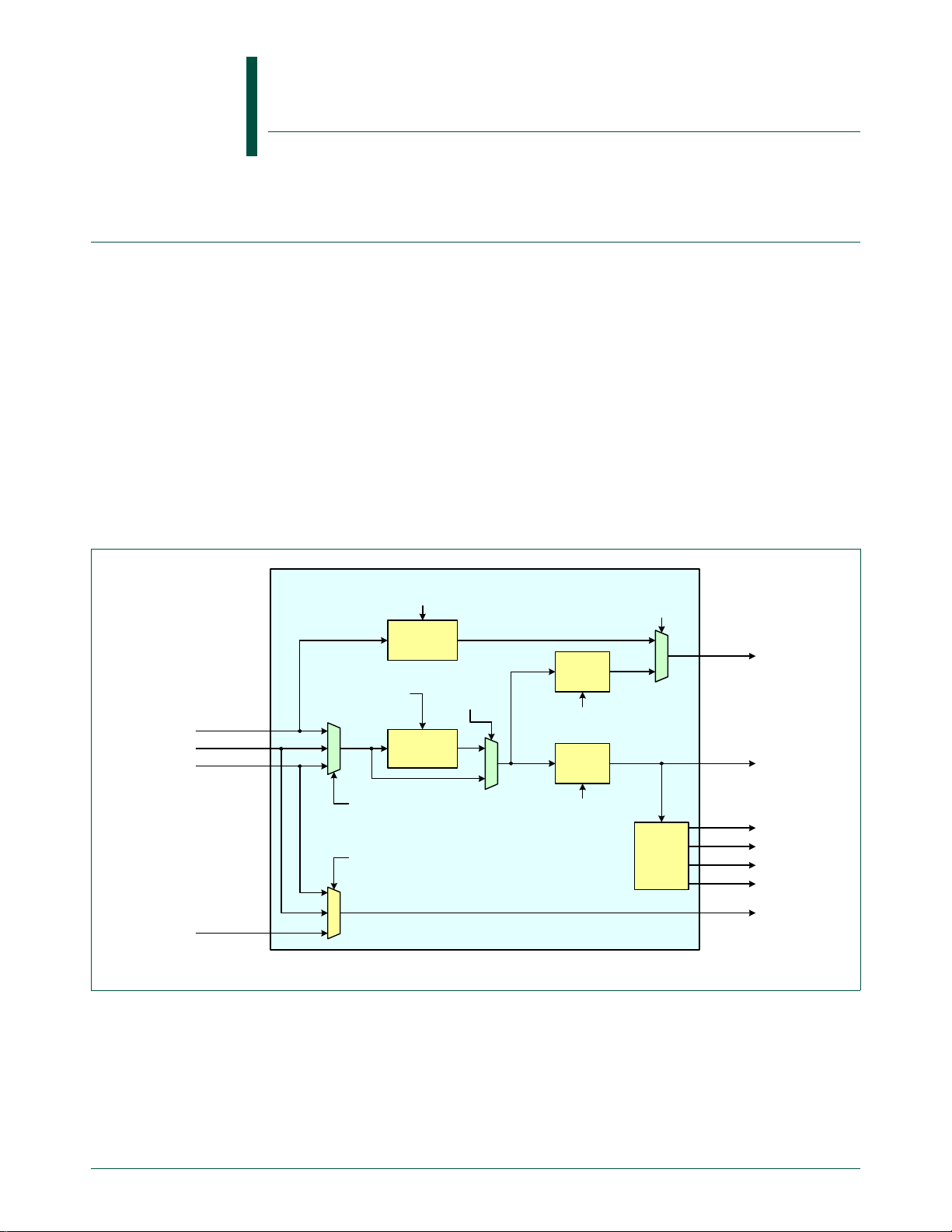
`
USB
Clock
Divider
osc_clk
irc_osc
system clock select
CLKSRCSEL[1:0]
USB PLL settings
(PLL1...)
USB clock divider setting
USBCLKCFG[3:0]
PCLK_WDT
Peripheral
Clock
Divider
wd_clk
usb_clk
pclk1
pclk8
pclk4
pclk2
USB PLL
(PLL1)
main PLL
settings
(PLL0...)
USB PLL
select
(PLL1CON)
Main PLL
(PLL0)
CPU
Clock
Divider
pllclk
CPU PLL
select
(PLL0CON)
cclk
watchdog clock select
WDCLKSEL[1:0]
rtc_clk
CPU clock divider setting
CCLKCFG[7:0]
sysclk
UM10360
Chapter 4: LPC17xx Clocking and power control
Rev. 2 — 19 August 2010 User manual
4.1 Summary of clocking and power control functions
This section describes the generation of the various clocks needed by the LPC17xx and
options of clock source selection, as well as power control and wake-up from reduced
power modes. Functions described in the following subsections include:
• Oscillators
• Clock source selection
• PLLs
• Clock dividers
• APB dividers
• Power control
• Wake-up timer
• External clock output
Fig 7. Clock generation for the LPC17xx
UM10360 All information provided in this document is subject to legal disclaimers. © NXP B.V. 2010. All rights reserved.
User manual Rev. 2 — 19 August 2010 29 of 840
Page 30

NXP Semiconductors
4.2 Register description
All registers, regardless of size, are on word address boundaries. Details of the registers
appear in the description of each function.
T able 14. Summary of system control registers
Name Description Access Reset value Address
Clock source selection
CLKSRCSEL Clock Source Select Register R/W 0 0x400F C10C
Phase Locked Loop (PLL0, Main PLL)
PLL0CON PLL0 Control Register R/W 0 0x400F C080
PLL0CFG PLL0 Configuration Register R/W 0 0x400F C084
PLL0STAT PLL0 Status Register RO 0 0x400F C088
PLL0FEED PLL0 Feed Register WO NA 0x400F C08C
Phase Locked Loop (PLL1, USB PLL)
PLL1CON PLL1 Control Register R/W 0 0x400F C0A0
PLL1CFG PLL1 Configuration Register R/W 0 0x400F C0A4
PLL1STAT PLL1 Status Register RO 0 0x400F C0A8
PLL1FEED PLL1 Feed Register WO NA 0x400F C0AC
Clock dividers
CCLKCFG CPU Clock Configuration Register R/W 0 0x400F C104
USBCLKCFG USB Clock Configuration Register R/W 0 0x400F C108
PCLKSEL0 Peripheral Clock Selection register 0. R/W 0 0x400F C1A8
PCLKSEL1 Peripheral Clock Selection register 1. R/W 0 0x400F C1AC
Power control
PCON Power Control Register R/W 0 0x400F C0C0
PCONP Power Control for Peripherals Register R/W 0x03BE 0x400F C0C4
Utility
CLKOUTCFG Clock Output Configurat ion Register R/W 0 0x400F C1C8
UM10360
Chapter 4: LPC17xx Clocking and power control
UM10360 All information provided in this document is subject to legal disclaimers. © NXP B.V. 2010. All rights reserved.
User manual Rev. 2 — 19 August 2010 30 of 840
Page 31

NXP Semiconductors
4.3 Oscillators
The LPC17xx includes three independent oscillators. These are the Main Oscillator, the
Internal RC Oscillator, and the RTC oscillator. Each oscillator can be used for more than
one purpose as required in a particular application. This can be seen in Figure 7
Following Reset, the LPC17xx will operate from the Internal RC Oscillator until switched
by software. This allows systems to operate without any external crystal, and allows the
boot loader code to operate at a known frequency.
4.3.1 Internal RC oscillator
The Internal RC Oscillator (IRC) may be used as the clock source for the watchdog timer,
and/or as the clock that drives PLL0 and subsequently the CPU. The precision of the IRC
does not allow for use of the USB interface, which requires a much more precise time
base in order to comply with the USB specification. Also, the IRC should not be used with
the CAN1/2 block if the CAN baud rate is higher than 100 kbit/s.The nominal IRC
frequency is 4 MHz.
Upon power-up or any chip reset, the LPC17xx uses the IRC as the clock source.
Software may later switch to one of the other available clock sources.
UM10360
Chapter 4: LPC17xx Clocking and power control
.
4.3.2 Main oscillator
The main oscillator can be used as the clock source for the CPU, with or without using
PLL0. The main oscillator operates at frequencies of 1 MHz to 25 MHz. This frequency
can be boosted to a higher frequency, up to the maximum CPU operating frequency, by
the Main PLL (PLL0). The oscillator output is called OSC_CLK. The clock selected as the
PLL0 input is PLLCLKIN and the ARM processor clock frequency is referred to as CCLK
for purposes of rate equations, etc. elsewh er e in th is doc ume nt. The frequencies of
PLLCLKIN and CCLK are the same value unless the PLL0 is active and connected. Refer
to Section 4.5 “
The on-board oscillator in the LPC17xx can operate in one of two modes: slave mode and
oscillation mode.
In slave mode the input clock signal should be coupled by means of a capacitor of 100 pF
in Figure 8, drawing a), with an amplitude between 200 mVrms and 1000 mVrms.
(C
C
This corresponds to a square wave signal with a signal swing of betwee n 280 mV and 1.4
V. The XTAL2 pin in this configuration can be left unconnected.
External components and models used in oscillation mode are shown in Figure 8
drawings b and c, and in Table 15
integrated on chip, only a crysta l and the cap acit ances C
externally in case of fundamental mode oscillation (the fundamental frequency is
represented by L, C
parallel package capacitance and should not be larger than 7 pF. Parameters F
and C
are supplied by the crystal manufacturer.
P
PLL0 (Phase Locked Loop 0)” for details.
,
and Table 16. Since the feedback resistance is
and CX2 need to be connected
X1
and RS). Capacitance CP in Figure 8, drawing c, represents the
L
, CL, RS
C
UM10360 All information provided in this document is subject to legal disclaimers. © NXP B.V. 2010. All rights reserved.
User manual Rev. 2 — 19 August 2010 31 of 840
Page 32

NXP Semiconductors
LPC17xx LPC17xx
Clock
C
C
C
X1
C
X2
C
L
C
P
L
R
S
< = >
a) b) c)
Xtal
XTAL1 XTAL2
XTAL1 XTAL2
UM10360
Chapter 4: LPC17xx Clocking and power control
Fig 8. Oscillator modes and models: a) slave mode of operation, b) oscillation mode of operation, c) external
crystal model used for CX1/X2 evaluation
UM10360 All information provided in this document is subject to legal disclaimers. © NXP B.V. 2010. All rights reserved.
User manual Rev. 2 — 19 August 2010 32 of 840
T able 15. Recommended values for C
in oscillation mode (crystal and external
X1/X2
components parameters) low frequency mode (OSCRANGE = 0, see Table 13)
Fundamental oscillation
frequency F
OSC
Crystal load
capacitance C
Maximum crystal
series resistance R
L
External load
capacitors CX1,
S
CX2
1 MHz - 5 MHz 10 pF < 300 Ω 18 pF, 18 pF
20 pF < 300
30 pF < 300
5 MHz - 10 MHz 10 pF < 300
20 pF < 200
30 pF < 100
10 MHz - 15 MHz 10 pF < 160
20 pF < 60
15 MHz - 20 MHz 10 pF < 80
T able 16. Recommended values for C
in oscillation mode (crystal and external
X1/X2
components parameters) high frequency mode (OSCRANGE = 1, see Table 13
Fundamental oscillation
frequency F
OSC
Crystal load
capacitance C
L
Ω 39 pF, 39 pF
Ω 57 pF, 57 pF
Ω 18 pF, 18 pF
Ω 39 pF, 39 pF
Ω 57 pF, 57 pF
Ω 18 pF, 18 pF
Ω 39 pF, 39 pF
Ω 18 pF, 18 pF
Maximum crystal
series resistance R
External load
capacitors C
S
)
X1, CX2
15 MHz - 20 MHz 10 pF < 180 Ω 18 pF, 18 pF
20 pF < 100
20 MHz - 25 MHz 10 pF < 160
20 pF < 80
Since chip operation always begins using the Internal RC Oscillator, and the main
oscillator may not be used at all in some applications, it will only be started by software
request. This is accomplished by setting the OSCEN bit in the SCS register, as described
in Table 13
register) so that software can determine when the oscillator is running and stable. At that
. The main oscillator provides a status flag (the OSCSTAT bit in the SCS
Ω 39 pF, 39 pF
Ω 18 pF, 18 pF
Ω 39 pF, 39 pF
Page 33

NXP Semiconductors
point, software can control switching to the main oscillator as a clock source. Prior to
starting the main oscillator, a frequency range must be selected by configuring the
OSCRANGE bit in the SCS register.
4.3.3 RTC oscillator
The RTC oscillator provides a 1 Hz clock to the RTC and a 32 kHz clock output that can
be used as the clock source for PLL0 and CPU and/or the watchdog timer.
Remark: The RTC oscillator must not be used as a clock source when the PLL0 output is
selected to drive the USB controller. In this case select the main oscillator as clock source
for PLL0 (see also Table 17
UM10360
Chapter 4: LPC17xx Clocking and power control
).
UM10360 All information provided in this document is subject to legal disclaimers. © NXP B.V. 2010. All rights reserved.
User manual Rev. 2 — 19 August 2010 33 of 840
Page 34

NXP Semiconductors
4.4 Clock source selection multiplexer
Several clock sources may be chosen to drive PLL0 and ultimately the CPU and on-chip
peripheral devices. The clock sources available are the main oscillator, the RTC oscillator,
and the Internal RC oscillator.
The clock source selection can only be changed safely when PLL0 is not connected . For a
detailed description of how to change the clock source in a system using PLL0 see
Section 4.5.13 “
Note the following restrictions regarding the choice of clock sources:
• Only the main oscillator must be used (via PLL0) as the clock source for the USB
subsystem. The IRC or RTC oscillators do not provide the proper tolerances for this
use.
• The IRC oscillator should not be used (via PLL0) as the clock source for the CAN
controllers if the CAN baud rate is higher than 100 kbit/s.
4.4.1 Clock Source Select register (CLKSRCSEL - 0x400F C10C)
PLL0 setup sequence”.
UM10360
Chapter 4: LPC17xx Clocking and power control
The CLKSRCSEL register contains the bits that sel e ct the clock source for PLL0.
Table 17. Clock Source Select register (CLKSRCSEL - address 0x400F C10C) bit
description
Bit Symbol Value Description Reset
value
1:0 CLKSRC Selects the clock source for PLL0 as follows: 0
00 Selects the Internal RC oscillator as the PLL0 clock source
(default).
01 Selects the main oscillator as the PLL0 clock source.
Remark: Select the main oscillator as PLL0 clock source if the
PLL0 clock output is used for USB or for CAN with baudrates
> 100 kBit/s.
10 Selects the RTC oscillator as the PLL0 clock source.
1 1 Reserved, do not use this setting.
Warning: Improper setting of this value, or an incorrect sequence of
changing this value may result in incorrect operation of the device.
31:2 - 0 Reserved, user software should not write ones to reserved bits.
The value read from a reserved bit is not defined.
NA
UM10360 All information provided in this document is subject to legal disclaimers. © NXP B.V. 2010. All rights reserved.
User manual Rev. 2 — 19 August 2010 34 of 840
Page 35

NXP Semiconductors
4.5 PLL0 (Phase Locked Loop 0)
PLL0 accepts an input clock frequency in the range of 32 kHz to 50 MHz. The clock
source is selected in the CLKSRCSEL register (see Section 4.4
multiplied up to a high frequency, then divided down to provide the actual clock used by
the CPU, peripherals, and optionally the USB subsystem. Note that the USB subsystem
has its own dedicated PLL (see Section 4.6
maximum allowed for the CPU, which is 120 MHz on high speed versions (LPC1769 and
LPC1759), and 100 MHz on other versions.
4.5.1 PLL0 operation
The PLL input, in the range of 32 kHZ to 50 MHz, may initially be divided down by a value
"N", which may be in the range of 1 to 256. This input division provides a greater number
of possibilities in providing a wide range of output frequencies from the same input
frequency.
Following the PLL input divider is the PLL multiplier. This can multiply the input divider
output through the use of a Current Controlled Oscillator (CCO) by a value "M", in the
range of 6 through 512, plus additional values listed in Table 21
must be in the range of 275 MHz to 550 MHz. The multiplier works by dividing the CCO
output by the value of M, then using a phase-frequency detector to compare the divided
CCO output to the multiplier input. The error value is used to adjust the CCO frequency.
UM10360
Chapter 4: LPC17xx Clocking and power control
). The input frequency is
). PLL0 can produce a clock up to the
. The resulting frequency
There are additional dividers at the output of PLL0 to bring the frequency down to what is
needed for the CPU, peripherals, and potentially the USB subsystem. PLL0 output
dividers are described in the Clock Dividers section following the PLL0 description. A
block diagram of PLL0 is shown in Figure 9
PLL activation is controlled via the PLL0CON register. PLL0 multiplier and divider values
are controlled by the PLL0CFG register. These two registers are protected in order to
prevent accidental alteration of PLL0 parameters or dea ctivation of the PLL. Since all chip
operations, including the Watchdog Timer, could be dependent on PLL0 if so configured
(for example when it is providing the chip clock), accidental changes to the PLL0 setup
values could result in unexpected or fatal behavior of the microcontroller. The protection is
accomplished by a feed sequence similar to that of the Watchdog Timer. Details are
provided in the description of the PLL0FEED register.
PLL0 is turned off and bypassed following a chip Reset and by entering Power-down
mode. PLL0 must be configured, enabled, and connected to the system by software.
It is important that the setup procedure described in Section 4.5.13 “
sequence” is followed or PLL0 might not operate at all!
4.5.1.1 PLL0 and startup/boot code interaction
When there is no valid user code (determined by the checksum word) in the user flash or
the ISP enable pin (P2.10) is pulled low on startup, the ISP mode will be entered and the
boot code will setup the PLL with the IRC. Therefore it can not be assumed that the PLL is
disabled when the user opens a debug session to debug the application code. The user
startup code must follow the steps describe d in this chapter to disconnect the PLL.
PLL0 setup
UM10360 All information provided in this document is subject to legal disclaimers. © NXP B.V. 2010. All rights reserved.
User manual Rev. 2 — 19 August 2010 35 of 840
Page 36

NXP Semiconductors
N-DIVIDER
M-DIVIDER
NSEL
[7:0]
PHASE-
FREQUENCY
DETECTOR
FILTER CCO
/2
MSEL
[14:0]
PLOCK
PLLE
PLLC
pd
refclk
pllclkin
pllclk
4.5.2 PLL0 register description
PLL0 is controlled by the registers shown in Table 18. More detailed descriptions follow.
Warning: Improper setting of PLL0 values may result in incorrect operation of the
device!
Table 18. PLL0 registers
Name Description Access Reset
PLL0CON PLL0 Control Register. Holding register for
PLL0CFG PLL0 Configuration Register. Holding register for
PLL0STAT PLL0 Status Register. Read-back register for
PLL0FEED PLL0 Feed Register. This register enables
Chapter 4: LPC17xx Clocking and power control
updating PLL0 control bits. Values written to this
register do not take effect un ti l a valid PL L0 fee d
sequence has taken place.
updating PLL0 configuration values. Values
written to this register do not take effect until a
valid PLL0 feed sequence has taken place.
PLL0 control and configuration information. If
PLL0CON or PLL0CFG have been written to, but
a PLL0 feed sequence has not yet occurred, they
will not reflect the current PLL0 state. Reading
this register provides the actual values controlling
the PLL0, as well as the PLL0 status.
loading of the PLL0 control and configuration
information from the PLL0CON and PLL0CFG
registers into the shadow registers that actually
affect PLL0 operation.
UM10360
Address
[1]
value
R/W 0 0x400F C080
R/W 0 0x400F C084
RO 0 0x400F C088
WO NA 0x400F C08C
[1] Reset Value reflects the data stored in used bits only. It does not include reserved bits content.
Fig 9. PLL0 block diagram
4.5.3 PLL0 Control register (PLL0CON - 0x400F C080)
The PLL0CON register contains the bits that enable and connect PLL0. Enabling PLL0
UM10360 All information provided in this document is subject to legal disclaimers. © NXP B.V. 2010. All rights reserved.
User manual Rev. 2 — 19 August 2010 36 of 840
allows it to attempt to lock to the current settings of the multiplier and divider values.
Connecting PLL0 causes the processor and most chip functions to run from the PLL0
Page 37

NXP Semiconductors
output clock. Changes to the PLL0CON register do not take effect until a correct PLL0
feed sequence has been given (see Section 4.5.8 “
0x400F C08C)”).
Table 19. PLL Control register (PLL0CON - address 0x400F C080) bit description
Bit Symbol Description Reset
0 PLLE0 PLL0 Enable. When one, and after a valid PLL0 feed, this bit will activate
1 PLLC0 PLL0 Connect. Setting PLLC0 to one after PLL0 has been enabled and
31:2 - Reserved, user software should not write ones to reserved bits. The
PLL0 must be set up, enabled, and Lock established before it may be used as a clock
source. When switching from the oscillator clock to the PLL0 output or vice versa, internal
circuitry synchronizes the operation in order to ensure that glitches are not generated.
Hardware does not insure that PLL0 is locked before it is connected or automatically
disconnect PLL0 if lock is lost during operation. In the event of loss of lock on PLL0, it is
likely that the oscillator clock has become unstable and disconnecting PLL0 will not
remedy the situation.
UM10360
Chapter 4: LPC17xx Clocking and power control
PLL0 Feed register (PLL0FEED -
PLL0 and allow it to lock to the requested frequency. See PLL0STAT
register, Table 22
locked, then followed by a valid PLL0 feed sequence causes PLL0 to
become the clock source for the CPU, AHB peripherals, and used to
derive the clocks for APB peripherals. The PLL0 output may potentially
be used to clock the USB subsystem if the frequency is 48 MHz. See
PLL0ST AT register, Table 22
value read from a reserved bit is not defined.
.
.
value
0
0
NA
4.5.4 PLL0 Configuration register (PLL0CFG - 0x400F C084)
The PLL0CFG register contains PLL0 multiplier and divider values. Changes to the
PLL0CFG register do not take effect until a correct PLL feed sequence has been given
(see Section 4.5.8 “
the PLL frequency , and multiplier and d ivider values are fo und in the Section4.5.10 “
frequency calculation”.
Table 20. PLL0 Configuration register (PLL0CFG - address 0x400F C084) bit description
Bit Symbol Description Reset
14:0 MSEL0 PLL0 Multiplier value. Supplies the value "M" in PLL0 frequency
15 - Reserved, user software should not write ones to reserved bits. The
23:16 NSEL0 PLL0 Pre-Divider value. Supplies the value "N" in PLL0 frequency
31:24 - Reserved, user software should not write ones to reserved bits. The
PLL0 Feed register (PLL0FEED - 0x400F C08C)”). Calculations for
calculations. The value stored here is M - 1. Supported values for M
are 6 through 512 and those listed in Table 21
Note: Not all values of M are needed, and therefore some are not
supported by hardware. For details on selecting values for MSEL0 see
Section 4.5.10 “
value read from a reserved bit is not defined.
calculations. The value stored here is N - 1. Supported values for N are
1 through 32.
Note: For details on selecting the right value for NSEL0 see
Section 4.5.10 “
value read from a reserved bit is not defined.
PLL0 frequency calculation”.
PLL0 frequency calculation”.
.
PLL0
value
0
NA
0
NA
UM10360 All information provided in this document is subject to legal disclaimers. © NXP B.V. 2010. All rights reserved.
User manual Rev. 2 — 19 August 2010 37 of 840
Page 38

NXP Semiconductors
Table 21. Multiplier values for PLL0 with a 32 kHz input
Multiplier
(M)
4272 1 279.9698 12085 2 396.0013
4395 1 288.0307 12207 2 399.9990
4578 1 300.0238 12817 2 419.9875
4725 1 309.6576 12817 3 279.9916
4807 1 315.0316 13184 2 432.0133
5127 1 336.0031 13184 3 288.0089
5188 1 340.0008 13672 2 448.0041
5400 1 353.8944 13733 2 450.0029
5493 1 359.9892 13733 3 300.0020
5859 1 383.9754 13916 2 455.9995
6042 1 395.9685 14099 2 461.9960
6075 1 398.1312 14420 3 315.0097
6104 1 400.0317 14648 2 479.9857
6409 1 420.0202 15381 2 504.0046
6592 1 432.0133 15381 3 336.0031
6750 1 442.3680 15564 3 340.0008
6836 1 448.0041 15625 2 512.0000
6866 1 449.9702 15869 2 519.9954
6958 1 455.9995 16113 2 527.9908
7050 1 462.0288 16479 3 359.9892
7324 1 479.9857 17578 3 383.9973
7425 1 486.6048 18127 3 395.9904
7690 1 503.9718 18311 3 400.0099
7813 1 512.0328 19226 3 419.9984
7935 1 520.0282 19775 3 431.9915
8057 1 528.0236 20508 3 448.0041
8100 1 530.8416 20599 3 449.9920
8545 2 280.0026 20874 3 455.9995
8789 2 287.9980 21149 3 462.0070
9155 2 299.9910 21973 3 480.0075
9613 2 314.9988 23071 3 503.9937
10254 2 336.0031 23438 3 512.0109
10376 2 340.0008 23804 3 520.0063
10986 2 359.9892 24170 3 528.0017
11719 2 384.0082
Pre-divide
(N)
F
CCO
UM10360
Chapter 4: LPC17xx Clocking and power control
Multiplier
(M)
Pre-divide
(N)
F
CCO
UM10360 All information provided in this document is subject to legal disclaimers. © NXP B.V. 2010. All rights reserved.
User manual Rev. 2 — 19 August 2010 38 of 840
Page 39

NXP Semiconductors
4.5.5 PLL0 Status register (PLL0STAT - 0x400F C088)
The read-only PLL0STAT register provides the actual PLL0 parameters that are in effect
at the time it is read, as well as PLL0 stat us. PLL0STAT may disagree with values fou nd in
PLL0CON and PLL0CFG because changes to those registers do not take effect until a
proper PLL0 feed has occurred (see Section 4.5.8 “
0x400F C08C)”).
T able 22. PLL Status register (PLL0STAT - address 0x400F C088) bit description
Bit Symbol Description Reset
14:0 MSEL0 Read-back for the PLL0 Multiplier value. This is the value currently
15 - Reserved, user software should not write ones to reserved bits.
23:16 NSEL0 Read-back for the PLL0 Pre-Divider value. This is the value
24 PLLE0_STAT Read-back for the PLL0 Enable bit. This bit reflects the state of the
25 PLLC0_STAT Read-back for the PLL0 Connect bit. This bit reflects the state of
26 PLOCK0 Reflects the PLL0 Lock status. When zero, PL L0 is not locked.
31:27 - Reserved, user software should not write ones to reserved bits.
UM10360
Chapter 4: LPC17xx Clocking and power control
PLL0 Feed register (PLL0FEED -
used by PLL0, and is one less than the actual multiplier.
The value read from a reserved bit is not defined.
currently used by PLL0, and is one less than the actual divider.
PLEC0 bit in PLL0CON (see Table19
When one, PLL0 is currently enabled. When zero, PLL0 is turned
off. This bit is automatically cleared when Power-down mode is
entered.
the PLLC0 bit in PLL0CON (see Table 19
When PLLC0 and PLLE0 are both one, PLL0 is connected as the
clock source for the CPU. When either PLLC0 or PLLE0 is zero,
PLL0 is bypassed. This bit is automatically cleared when
Power-down mode is entered.
When one, PLL0 is locked onto the requested frequency. See text
for details.
The value read from a reserved bit is not defined.
) after a valid PLL0 feed.
) after a valid PLL0 feed.
value
0
NA
0
0
0
0
NA
4.5.6 PLL0 Interrupt: PLOCK0
The PLOCK0 bit in the PLL0STAT register reflects the lock status of PLL0. When PLL0 is
enabled, or parameters are changed, PL L0 requires some time to establish lo ck under the
new conditions. PLOCK0 can be monitored to determine when PLL0 may be connected
for use. The value of PLOCK0 may not be stable when the PLL reference frequency
(F
, the frequency of REFCLK, which is equal to the PLL input frequency divided by the
REF
pre-divider value) is less than 100 kHz or greater than 20 MHz. In these cases, the PLL
may be assumed to be stable after a start-up time has passed. This time is 500 μs when
FREF is greater than 400 kHz and 200 / FREF seconds when FREF is less than 400 kHz
PLOCK0 is connected to the interrupt controller. This allows for software to turn on PLL0
and continue with other functions without having to wait for PLL0 to achieve lock. When
the interrupt occurs, PLL0 may be connected, and the interrupt disabled. PLOCK0
appears as interrupt 32 in Table 50
is locked, so if the interrupt is used, the interrupt service routine must disable the PLOCK0
interrupt prior to exiting.
UM10360 All information provided in this document is subject to legal disclaimers. © NXP B.V. 2010. All rights reserved.
User manual Rev. 2 — 19 August 2010 39 of 840
. Note that PLOCK0 remains asserted whenever PLL0
Page 40

NXP Semiconductors
4.5.7 PLL0 Modes
The combinations of PLLE0 and PLLC0 are shown in Table 23.
Table 23. PLL control bit combinations
PLLC0 PLLE0 PLL Function
0 0 PLL0 is turned off and disconnected. PLL0 outputs the unmodified clock input.
0 1 PLL0 is active, but not yet connected. PLL0 can be connected after PLOCK0 is
1 0 Same as 00 combination. This prevents the possibility of PLL0 being connected
1 1 PLL0 is active and has been connected as the system clock source.
4.5.8 PLL0 Feed register (PLL0FEED - 0x400F C08C)
A correct feed sequence must be written to the PLL0FEED register in order for cha nges to
the PLL0CON and PLL0CFG registers to take effect. The feed sequence is:
1. Write the value 0xAA to PLL0FEED.
2. Write the value 0x55 to PLL0FEED.
UM10360
Chapter 4: LPC17xx Clocking and power control
asserted.
without also being enabled.
The two writes must be in the correct sequence, and there must be no other register
access in the same address space (0x400F C000 to 0x400F FFFF) between them.
Because of this, it may be necessary to disable interrupt s for the duration of the PLL0 feed
operation, if there is a possibility that an interrupt service routine could write to another
register in that space. If either of the feed values is incorrect, or one of the previously
mentioned conditions is not met, any changes to the PLL0CON or PLL0CFG register will
not become effective.
Table 24. PLL Feed register (PLL0FEED - address 0x4 00F C08C) bit des cription
Bit Symbol Description Reset
7:0 PLL0FEED The PLL0 feed sequence must be written to this register in order for
PLL0 configuration and control register changes to take effect.
31:8 - Reserved, user software should not write ones to reserved bits. The
value read from a reserved bit is not defined.
4.5.9 PLL0 and Power-down mode
Power-down mode automatically turns off and disconnects PLL0. Wake-up from
Power-down mode does not automatically restore PLL0 settings, this must be done in
software. T ypically , a r outine to activate PLL0, wait for lock, and then connect PLL0 can be
called at the beginning of any interrupt service routine that might be called due to the
wake-up. It is important not to attempt to restart PLL0 by simply feeding it when execution
resumes after a wake-up from Power-down mode. This would enable and connect PLL0
at the same time, before PLL lock is established.
value
0x00
NA
4.5.10 PLL0 frequency calculation
PLL0 equations use the following parameters:
UM10360 All information provided in this document is subject to legal disclaimers. © NXP B.V. 2010. All rights reserved.
User manual Rev. 2 — 19 August 2010 40 of 840
Page 41

NXP Semiconductors
Table 25. PLL frequency parameter
Parameter Description
F
IN
F
CCO
N PLL0 Pre-divider value from the NSEL0 bits in the PLL0CFG register (PLL0CFG
M PLL0 Multiplier value from the MSEL0 bits in the PLL0CFG register (PLL0CFG
F
REF
The PLL0 output frequency (when PLL0 is both active and connected) is given by:
F
CCO
PLL inputs and settings must meet the following:
• F
• F
Chapter 4: LPC17xx Clocking and power control
the frequency of PLLCLKIN from the Clock Source Selection Multiplexer.
the frequency of the PLLCLK (output of the PLL Current Controlled Oscillator)
NSEL0 field + 1). N is an integer from 1 through 32.
MSEL0 field + 1). Not all potential values are supported. See below.
PLL internal reference frequency, FIN divided by N.
= (2 × M × FIN) / N
is in the range of 32 kHz to 50 MHz.
IN
is in the range of 275 MHz to 550 MHz.
CCO
UM10360
The equation can be solved for other PLL parameters:
M = (F
N = (2 × M × F
FIN = (F
× N) / (2 × FIN)
CCO
IN
× N) / (2 × M)
CCO
) / F
CCO
Allowed values for M:
At higher oscillator frequencies, in the MHz range, values of M from 6 through 512 are
allowed. This supports the entire useful range of both the main oscillator and the IRC.
For lower frequencies, specifically when the RTC is used to clock PLL0, a set of 65
additional M values have been selected for supporting baud rate generation, CAN
operation, and obtaining integer MHz frequencies. Th ese values are shown in Table 26
.
UM10360 All information provided in this document is subject to legal disclaimers. © NXP B.V. 2010. All rights reserved.
User manual Rev. 2 — 19 August 2010 41 of 840
Page 42

NXP Semiconductors
Table 26. Additional Multiplier Values for use with a Low Frequency Clock Input
UM10360
Chapter 4: LPC17xx Clocking and power control
Low Frequency PLL Multipliers
4272 4395 4578 4725 4807
5127 5188 5400 5493 5859
6042 6075 6104 6409 6592
6750 6836 6866 6958 7050
7324 7425 7690 7813 7935
8057 8100 8545 8789 9155
9613 10254 10376 10986 11719
12085 12207 12817 13184 13672
13733 13916 14099 14420 14648
15381 15564 15625 15869 16113
16479 17578 18127 18311 19226
19775 20508 20599 20874 21149
21973 23071 23438 23804 24170
4.5.1 1 Procedure for determining PLL0 settings
PLL0 parameter determination can be simplified by using a spreadsheet available from
NXP. To determine PLL0 parameters by hand, the follo win g ge n er al procedure may be
used:
1. Determine if the application requires use of the USB interface, and whether it will be
clocked from PLL0. The USB requires a 50% duty cycle clock of 48 MHz within a very
small tolerance, which means that F
(i.e. an integer multiple of 96 MHz), within a very small tolerance.
2. Choose the desired pro cessor operating frequency (CCLK). This may be based on
processor throughput requirements, need to support a specific set of UART baud
rates, etc. Bear in mind that peripheral devices may be running from a lower clock
frequency than that of the processor (see Section 4.7 “
Section 4.8 “
Power control” on page 58). Find a value for F
multiple of the desired CCLK frequency, bearing in mind the requirement for USB
support in [1] above, and that lower values of F
3. Choose a value for the PLL input frequency (F
the main oscillator, the RTC oscillator, or the on-chip RC oscillator. For USB support,
the main oscillator should be used. Bear in mind that if PLL1 rather than PLL0 is used
to clock the USB subsystem, this affects the choice of the main oscillator frequency.
4. Calculate values for M and N to produce a sufficiently accurate F
desired M value -1 will be written to the MSEL0 field in PLL0CFG. The desired N value
-1 will be written to the NSEL0 field in PLL0CFG.
must be an even integer multiple of 48 MHz
CCO
IN
Clock dividers” on page 54 and
that is close to a
CCO
result in lower power dissipation.
CCO
). This can be a clock obtained from
frequency. The
CCO
In general, it is better to use a smaller value for N, to reduce the level of multiplication that
must be accomplished by the CCO. Due to the difficulty in finding the best values in some
cases, it is recommended to use a spreadsheet or similar method to show many
possibilities at once, from which an overall best choice may be selected. A spreadsheet is
available from NXP for this purpose.
UM10360 All information provided in this document is subject to legal disclaimers. © NXP B.V. 2010. All rights reserved.
User manual Rev. 2 — 19 August 2010 42 of 840
Page 43

NXP Semiconductors
4.5.12 Examples of PLL0 settings
The following table gives a summary of examples that illustrate selecting PLL0 values
based on different system requirements.
T able 27. Summary of PLL0 examples
Example Description
UM10360
Chapter 4: LPC17xx Clocking and power control
1 • The PLL0 clock source is 10 MHz.
• PLL0 is not used as the USB clock source, or the USB interface is not used.
• The desired CPU clock is 100 MHz.
2 • The PLL0 clock source is 4 MHz.
• PLL0 is used as the USB clock source.
• The desired CPU clock is 60 MHz.
3 • The PLL0 clock source is the 32.768 kHz RTC clock.
• PLL0 is not used as the USB clock source, or the USB interface is not used.
• The desired CPU clock is 72 MHz.
Example 1
Assumptions:
• The USB interface will not be used in the application, or will be clocked by PLL1.
• The desired CPU rate is 100 MHz.
• An external 10 MHz crystal or clock source will be used as the system clock source.
Calculations:
M = (F
A smaller value for the PLL pre-divide (N) as well as a smaller value of the multiplier (M),
both result in better PLL operational stability and lower output jitter. Lower values of F
also save power. So, the process of determining PLL setup parameters involves looking
for the smallest N and M values giving the lowest F
CPU and/or USB clocks. It is usually easier to work backward from the desired output
clock rate and determine a target F
the available input clock.
Potential precise values of F
example, it is clear that the smallest frequency for F
clock rate and is within the PLL0 operating range of 275 to 550 MHz is 300 MHz
(3 × 100 MHz).
× N) / (2 × FIN)
CCO
value that will support the required
CCO
rate, then find a way to obtain that F
CCO
are integer multiples of the desired CPU clock. In this
CCO
that can produce the desired CPU
CCO
CCO
CCO
rate from
Assuming that the PLL pre-divide is 1 (N = 1), the equation above gives
6
M = ((300 × 10
× 1) / (2 × 10 × 106) = 300 / 20 = 15. Since the result is an integer , there is
no need to look any further for a good set of PLL0 configuration value s. The va lue written
to PLL0CFG would be 0x0E (N - 1 = 0; M - 1 = 14 gives 0x0E).
The PLL output must be further divided in order to produce the CPU clock. This is
accomplished using a separate divider that is described later in this chapter, see
Section 4.7.1
UM10360 All information provided in this document is subject to legal disclaimers. © NXP B.V. 2010. All rights reserved.
User manual Rev. 2 — 19 August 2010 43 of 840
.
Page 44

NXP Semiconductors
Example 2
Assumptions:
• The USB interface will be used in the application and will be clocked from PLL0.
• The desired CPU rate is 60 MHz.
• An external 4 MHz crystal or clock source will be used as the system clock source.
Calculations:
UM10360
Chapter 4: LPC17xx Clocking and power control
This clock source could be the Internal RC oscillator (IRC).
M = (F
× N) / (2 × FIN)
CCO
Because supporting USB requires a precise 48 MHz clock with a 50% duty cycle, that
need must be addressed first. Potential precise values of F
are integer multiples of the
CCO
2 × the 48 MHz USB clock. The 2 × insures that the clock has a 50% duty cycle, which
would not be the case for a division of the PLL output by an odd number.
The possibilities for the F
MHz. The smallest frequency for F
rate when the USB is used are 288 MHz, 384 MHz, and 480
CCO
that can produce a valid USB clock rate and is
CCO
within the PLL0 operating range is 288 MHz (3 × 2 × 48 MHz).
Star t by assuming N = 1, since this produces the smallest multiplier needed for PLL0. So,
6
M = ((288 × 10
) × 1) / (2 × (4 × 106)) = 288 / 8 = 36. The result is an integer, which is
necessary to obtain a precise USB clock. The value written to PLL0CFG would be 0x23
(N - 1 = 0; M - 1 = 35 = 0x23).
The potential CPU clock rate can be determined by dividing F
frequency: 288 × 10
6
/60× 106= 4.8. The nearest integer value for the CPU Clock
by the desired CPU
CCO
Divider is then 5, giving us 57.6 MHz as the nearest value to the desired CPU clock rate.
If it is important to obtain exactly 60 MHz, an F
down to both 48 MHz and 60 MHz. As previously noted, the possibilities for the F
rate must be found that can be divided
CCO
CCO
rate
when the USB is used are 288 MHz, 384 MHz, and 480 MHz. Of these, only is 480 MHz is
also evenly divisible by 60. Divided by 10, this gives the 48 MHz with a 50% duty cycle
needed by the USB subsystem. Divided by 8, it gives 60 MHz for the CPU clock. PLL0
settings for 480 MHz are N = 1 and M = 60.
The PLL output must be further divided in order to produce both the CPU clock and the
USB clock. This is accomplished using separate dividers that are described later in this
chapter. See Section 4.7.1
UM10360 All information provided in this document is subject to legal disclaimers. © NXP B.V. 2010. All rights reserved.
User manual Rev. 2 — 19 August 2010 44 of 840
and Section 4.7.2.
Page 45

NXP Semiconductors
Example 3
Assumptions:
• The USB interface will not be used in the application, or will be clocked by PLL1.
• The desired CPU rate is 72 MHz
• The 32.768 kHz RTC clock source will be used as the system clock source
Calculations:
UM10360
Chapter 4: LPC17xx Clocking and power control
M = (F
× N) / (2 × FIN)
CCO
The smallest integer multiple of the desired CPU clock rate that is within the PLL0
operating range is 288 MHz (4 × 72 MHz).
6
Using the equation above and assuming that N = 1, M = ((288 × 10
) × 1) / (2 × 32,768) =
4,394.53125. This is not an integer, so th e CPU frequency will not be exactly 72 MHz with
this setting. Since this example is less obvious, it may be useful to make a table of
possibilities for different values of N (see below).
Table 28. Potential values for PLL example
N M M Rounded F
1 4394.53125 4395 32768 288.0307 72.0077 0.0107
2 8789.0625 8789 16384 287.9980 71.9995 -0.0007
3 13183.59375 13184 10922.67 288.0089 72.0022 0.0031
4 17578.125 17578 8192 287.9980 71.9995 -0.0007
5 21972.65625 21973 6553.6 288.0045 72.0011 0.0016
in Hz
REF
(FIN / N)
F
(F
CCO
in MHz
x M)
REF
CCLK in MHz
(F
/ 4)
CCO
% Error
(CCLK-72) / 72
Beyond N = 5, the value of M is out of range or not supported, so the table stops at that
point. In the third column of the table, the calculated M value is rounded to the nearest
integer. If this results in CCLK being above the maximum operating frequency, it is
allowed if it is not more than 1/2 % above the maximum freque n cy.
In general, larger values of F
result in a more stable PLL when the input clock is a low
REF
frequency. Even the first table entry shows a very small error of just over 1 hundred th of a
percent, or 107 parts per million (ppm). If that is not accurate enough in the application,
the second case gives a much smaller error of 7 ppm. There are no allowed combinations
that give a smaller error than that.
Remember that when a frequency below about 1 MHz is used as the PLL0 clock source,
not all multiplier values are available. As it turns out, all of the rounded M values found in
Table 28
of this example are supported, which may be confirmed in Table 26. If PLL0
calculations suggest use of unsupported multiplier values, those values must be
disregarded and other values examined to find the best fit.
The value written to PLL0CFG for the second table entry would be 0x12254
(N - 1 = 1 = 0x1; M - 1 = 8788 = 0x2254).
The PLL output must be further divided in order to produce the CPU clock. This is
accomplished using a separate divider that is described later in this chapter, see
Section 4.7.1
UM10360 All information provided in this document is subject to legal disclaimers. © NXP B.V. 2010. All rights reserved.
User manual Rev. 2 — 19 August 2010 45 of 840
.
Page 46

NXP Semiconductors
4.5.13 PLL0 setup sequence
The following sequence must be followed step by step in order to have PLL0 initialized
and running:
1. Disconnect PLL0 with one feed sequence if PLL0 is a lready connected.
2. Disable PLL0 with one feed sequence.
3. Change the CPU Clock Divider setting to speed up operation without PLL0, if desired.
4. Write to the Clock Source Selection Contr ol register to change the clock source if
5. Write to the PLL0CFG and make it effective with one feed sequence. The PLL0CFG
6. Enable PLL0 with one feed sequence.
7. Change the CPU Clock Divider setting for the operation with PLL0. It is critical to do
8. W ait for PLL0 to achieve lock by monito ring the PLOCK0 bit in the PLL0STAT register ,
9. Connect PLL0 with one feed sequence.
UM10360
Chapter 4: LPC17xx Clocking and power control
needed.
can only be updated when PLL0 is disabled.
this before connecting PLL0.
or using the PLOCK0 interrupt, or wait for a fixed time when the input clock to PLL0 is
slow (i.e. 32 kHz). The value of PLOCK0 may not be stable when the PLL reference
frequency (FREF, the frequency of REFCLK, which is equal to the PLL input
frequency divided by the pre-divider value) is less than 100 kHz or greater than
20 MHz. In these cases, the PLL may be assumed to be stable after a start-up time
has passed. This time is 500 µs when FREF is greater than 400 kHz and 200 / FREF
seconds when FREF is less than 400 kHz.
It is very important not to merge any steps above. For example, do not update the
PLL0CFG and enable PLL0 simultaneously with the same feed sequence.
UM10360 All information provided in this document is subject to legal disclaimers. © NXP B.V. 2010. All rights reserved.
User manual Rev. 2 — 19 August 2010 46 of 840
Page 47

NXP Semiconductors
4.6 PLL1 (Phase Locked Loop 1)
PLL1 receives its clock input from the main oscillator only and can be used to provide a
fixed 48 MHz clock only to the USB subsystem. This is an option in addition to the
possibility of generating the USB clock from PLL0.
PLL1 is disabled and powered off on reset. If PLL1 is left disabled, the USB clock can be
supplied by PLL0 if everything is set up to provide 48 MHz through that route. If PLL1 is
enabled and connected via the PLL1CON register (see Section 4.6.2
selected to drive the USB subsystem (see Figure 7
PLL1 activation is controlled via the PLL1CON register . PLL1 mu ltiplier and divide r values
are controlled by the PLL1CFG register. These two registers are protected in order to
prevent accidental alteration of PLL1 parameters or deactivation of PLL1. The protection
is accomplished by a feed sequence similar to that of the Watchdog Timer. Details are
provided in the description of the PLL1FEED register.
PLL1 accepts an input clock frequency in the range of 10 MHz to 25 MHz only. The input
frequency is multiplied up to the range of 48 MHz for the USB clock using a Current
Controlled Oscillator (CCO). The multiplier can be an integer value from 1 to 32 (for USB,
the multiplier value cannot be higher than 4. The CCO operates in the range of 156 MHz
to 320 MHz, so there is an additional divider in the loop to keep the CCO within its
frequency range while PLL1 is providing the desired output frequency. The output divider
may be set to divide by 2, 4, 8, or 16 to produce the output clock. Since the minimum
output divider value is 2, it is insured that the output of PLL1 has a 50% duty cycle. A
block diagram of PLL1 is shown in Figure 10
UM10360
Chapter 4: LPC17xx Clocking and power control
), it is automatically
).
.
4.6.1 PLL1 register description
PLL1 is controlled by the registers shown in Table 29. More detailed descriptions follow.
Writes to any unused bits are ignored. A read of any unused bits will return a logic zero.
Warning: Improper setting of PLL1 values may result in incorrect operation of the
USB subsystem!
Table 29. PLL1 registers
Name Description Access Reset
PLL1CON PLL1 Control Register. Holding register for
updating PLL1 control bits. Values written to this
register do not take effect until a valid PLL1 feed
sequence has taken place.
Address
[1]
value
R/W 0 0x400F C0A0
UM10360 All information provided in this document is subject to legal disclaimers. © NXP B.V. 2010. All rights reserved.
User manual Rev. 2 — 19 August 2010 47 of 840
Page 48

NXP Semiconductors
100416
PLL output
clock
Divide by 2P
Phase
Detector
PLOCK
PLLSTAT[10]
Current-
Controlled
Oscillator
Fcco
PSEL
PLLSTAT[6:5]
PLL input
clock
Divide by M
MSEL
PLLSTAT[4:0]
Table 29. PLL1 registers
Name Description Access Reset
PLL1CFG PLL1 Configuration Register. Holding register
PLL1STAT PLL1 Status Register. Read-back register for
PLL1FEED PLL 1 Feed Register. This register enables
Chapter 4: LPC17xx Clocking and power control
for updating PLL1 configuration values. Values
written to this register do not take effect until a
valid PLL1 feed sequence has taken place.
PLL1 control and configuration information. If
PLL1CON or PLL1CFG have been written to,
but a PLL1 feed sequence has not yet occurred,
they will not reflect the current PLL1 state.
Reading this register provides the actual values
controlling PLL1, as well as PLL1 status.
loading of PLL1 control and configuration
information from the PLL1CON and PLL1CFG
registers into the shadow registers that actually
affect PLL1 operation.
UM10360
Address
[1]
value
R/W 0 0x400F C0A4
RO 0 0x400F C0A8
WO NA 0x400F C0AC
[1] Reset Value reflects the data stored in used bits only. It does not include reserved bits content.
Fig 10. PLL1 block diagram
4.6.2 PLL1 Control register (PLL1CON - 0x400F C0A0)
The PLL1CON register contains the bits that enable and connect PLL1. Enabling PLL1
allows it to attempt to lock to the current settings of the multiplier and divider values.
Connecting PLL1 causes the USB subsystem to run from the PLL1 output clock. Changes
to the PLL1CON register do not take effect until a corre ct PLL feed sequence has been
given (see Section 4.6.6
and Section 4.6.3).
UM10360 All information provided in this document is subject to legal disclaimers. © NXP B.V. 2010. All rights reserved.
User manual Rev. 2 — 19 August 2010 48 of 840
Page 49

NXP Semiconductors
Table 30. PLL1 Control register (PLL1CON - address 0x400F C0A0) bit description
Bit Symbol Description Reset
0 PLLE1 PLL1 Enable. When one, and after a valid PLL1 feed, this bit will
1 PLLC1 PLL1 Connect. Setting PLLC to one after PLL1 has been enabled and
31:2 - Reserved, user software should not write ones to reserved bits. The
PLL1 must be set up, enabled, and lock established before it may be used as a clock
source for the USB subsystem. The hardware does not insure that the PLL is locked
before it is connected nor does it automatically disconnect the PLL if lock is lost during
operation.
4.6.3 PLL1 Configuration register (PLL1CFG - 0x400F C0A4)
UM10360
Chapter 4: LPC17xx Clocking and power control
activate PLL1 and allow it to lock to the requested frequency. See
PLL1STAT register, Table 32
locked, then followed by a valid PLL1 feed sequence causes PLL1 to
become the clock source for the USB subsystem via the USB clock
divider. See PLL1STAT register, Table 32
value read from a reserved bit is not defined.
.
.
value
0
0
NA
The PLL1CFG register contains the PLL1 multiplier and divider values. Chan ges to the
PLL1CFG register do not take effect until a correct PLL1 feed sequence has been given
(see Section 4.6.6
are found in Section 4.6.9
Table 31. PLL Configuration register (PLL1CFG - address 0x400F C0A4) bit description
Bit Symbol Description Reset
4:0 MSEL1 PLL1 Multiplier value. Supplies the value "M" in the PLL1 frequency
6:5 PSEL1 PLL1 Divider value. Supplies the value "P" in the PLL1 frequency
31:7 - Reserved, user software should not write ones to reserved bits. The
). Calculations for the PLL1 frequency, and multiplier and divider values
.
calculations.
Note: For details on selecting the right value for MSEL1 see
Section 4.6.8
calculations.
Note: For details on selecting the right value for PSEL1 see
Section 4.6.8
value read from a reserved bit is not defined.
.
.
4.6.4 PLL1 Status register (PLL1STAT - 0x400F C0A8)
The read-only PLL1STAT register provides the actual PLL1 parameters that are in effect
at the time it is read, as well as the PLL1 status. PLL1STAT may disagree with values
found in PLL1CON and PLL1CFG because changes to those registers do not take effect
until a proper PLL1 feed has occurred (see Section 4.6.6 “
- 0x400F C0AC)”).
PLL1 Feed register (PLL1FEED
value
0
0
NA
UM10360 All information provided in this document is subject to legal disclaimers. © NXP B.V. 2010. All rights reserved.
User manual Rev. 2 — 19 August 2010 49 of 840
Page 50

NXP Semiconductors
Table 32. PLL1 Status register (PLL1STAT - address 0x400F C0A8) bit description
Bit Symbol Description Reset
4:0 MSEL1 Read-back for the PLL1 Multiplier value. This is the value currently
6:5 PSEL1 Read-back for the PLL1 Divider value. This is the value currently
7 - Reserved, user software should not write ones to reserved bits.
8 PLLE1_STAT Read-back for the PLL1 Enable bit. When one, PLL1 is currently
9 PLLC1_STAT Read-back for the PLL1 Connect bit. When PLLC and PLLE are
10 PLOCK1 Reflects the PLL1 Lock status. When zero, PL L1 is not locked.
31:11 - Reserved, user software should not write ones to reserved bits.
UM10360
Chapter 4: LPC17xx Clocking and power control
value
0
used by PLL1.
0
used by PLL1.
NA
The value read from a reserved bit is not defined.
0
activated. When zero, PLL1 is turned off. This bit is automatically
cleared when Power-down mode is activated.
0
both one, PLL1 is connected as the clock source for the
microcontroller. When either PLLC or PLLE is zero, PLL1 is
bypassed and the oscillator clock is used directly by the
microcontroller. This bit is automatically cleared when Power-down
mode is activated.
0
When one, PLL1 is locked onto the requested frequency.
NA
The value read from a reserved bit is not defined.
4.6.4.1 PLL1 modes
The combinations of PLLE1 and PLLC1 are shown in Table 33.
Table 33. PLL1 control bit combinat ions
PLLC1 PLLE1 PLL1 Function
0 0 PLL1 is turned off and disconnected.
0 1 PLL1 is active, but not yet connected. PLL1 can be connected after PLOCK1
is asserted.
1 0 Same as 00 combination. This prevents the possibility of PLL1 being
connected without also being enabled.
1 1 PLL1 is active and has been connected. The clock for the USB subsystem is
sourced from PLL1.
4.6.5 PLL1 Interrupt: PLOCK1
The PLOCK1 bit in the PLL1STAT register reflects the lock status of PLL1. When PLL1 is
enabled, or parameters are changed, the PLL requires some time to establish lock under
the new conditions. PLOCK1 can be monitored to determine when the PLL may be
connected for use.
PLOCK1 is connected to the interrupt controller. This allows for software to turn on the
PLL and continue with other functions without having to wait for the PLL to achieve lock.
When the interrupt occurs, the PLL may be connected, and the interrupt disabled.
PLOCK1 appears as interrupt 48 in Table 50
whenever PLL1 is locked, so if the interrupt is used, the interrupt service routine must
disable the PLOCK1 interrupt prior to exiting.
. Note that PLOCK1 remains asserted
UM10360 All information provided in this document is subject to legal disclaimers. © NXP B.V. 2010. All rights reserved.
User manual Rev. 2 — 19 August 2010 50 of 840
Page 51

NXP Semiconductors
4.6.6 PLL1 Feed register (PLL1FEED - 0x400F C0AC)
A correct feed sequence must be written to the PLL1FEED register in order for cha nges to
the PLL1CON and PLL1CFG registers to take effect. The feed sequence is:
1. Write the value 0xAA to PLL1FEED.
2. Write the value 0x55 to PLL1FEED.
The two writes must be in the correct sequence, and there must be no other register
access in the same address space (0x400F C000 to 0x400F FFFF) between them.
Because of this, it may be necessary to disable interrupts for the duration of the PLL feed
operation, if there is a possibility that an interrupt service routine could write to another
register in that space. If either of the feed values is incorrect, or one of the previously
mentioned conditions is not met, any changes to the PLL1CON or PLL1CFG register will
not become effective.
Table 34. PLL1 Feed register (PLL1FEED - address 0x400 F C0AC) bit description
Bit Symbol Description Reset
7:0 PLL1FEED The PLL1 feed sequence must be written to this register in order for
31:8 - Reserved, user software should not write ones to reserved bits. The
UM10360
Chapter 4: LPC17xx Clocking and power control
value
0x00
PLL1 configuration and control register changes to take effect.
NA
value read from a reserved bit is not defined.
4.6.7 PLL1 and Power-down mode
Power-down mode automatically turns off and disconnects activated PLL(s). Wake-up
from Power-down mode does not automatically restore PLL settings, this must be done in
software. Typically, a routine to activate the PLL, wait for lock, and then connect the PLL
can be called at the beginning of any interrupt service routine that might be called due to
the wake-up. It is important not to attempt to restart a PLL by simply feeding it when
execution resumes after a wake-up from Power-down mode. This would enable and
connect the PLL at the same time, before PLL lock is established.
If activity on the USB data lines is not selected to wake the microcontroller from
Power-down mode (see Section 4.8.8
the Main PLL (PLL0) and the USB PLL (PLL1) will be automatically be turned off and
disconnected when Power-down mode is invoked, as described above. However, if the
USB activity interrupt is enabled and USB_NEED_CLK = 1 (see Table 191
description of USB_NEED_CLK), it is not possible to go into Power-down mode and any
attempt to set the PD bit will fail, leaving the PLLs in the current state.
for details of wake up from reduced modes), both
for a
UM10360 All information provided in this document is subject to legal disclaimers. © NXP B.V. 2010. All rights reserved.
User manual Rev. 2 — 19 August 2010 51 of 840
Page 52

NXP Semiconductors
4.6.8 PLL1 frequency calculation
The PLL1 equations use the following parameters:
T able 35. Elements determining PLL frequency
Element Description
F
OSC
F
CCO
USBCLK the PLL1 output frequency (48 MHz for USB)
M PLL1 Multiplier value from the MSEL1 bits in the PLL1CFG register
P PLL1 Divider value from the PSEL1 bits in the PLL1CFG register
The PLL1 output frequency (when the PLL is both active and connected) is given by:
UM10360
Chapter 4: LPC17xx Clocking and power control
the frequency from the crystal oscillator
the frequency of the PLL1 current controlled oscillator
USBCLK = M × F
or USBCLK = F
OSC
CCO
/ (2 × P)
The CCO frequency can be computed as:
= USBCLK × 2 × P or F
F
CCO
CCO
= F
× M × 2 × P
OSC
The PLL1 inputs and settings must meet the following criteria:
• F
is in the range of 10 MHz to 25 MHz.
OSC
• USBCLK is 48 MHz.
• F
is in the range of 156 MHz to 320 MHz.
CCO
4.6.9 Procedure for determining PLL1 settings
The PLL1 configuration for USB may be determined as follows:
1. The desired PLL1 output frequency is USBCLK = 48 MHz.
2. Choose an oscillator frequency (F
multiple of F
meaning that the possible values for F
OSC
24 MHz.
3. Calculate the value of M to configure the MSEL1 bits. M = USBCLK / F
case, the possible values for M = 2, 3, or 4 (F
value written to the MSEL1 bits in PLL1CFG is M − 1 (see Table 37
4. Find a value for P to configure the PSEL1 bits, such that F
frequency limits of 156 MHz to 320 MHz. F
2 × P. It follows that P = 2 is the only P value to yield F
value written to the PSEL1 bits in PLL1CFG is ‘01’ for P= 2 (see Table 36
). USBCLK must be the whole (non-fractional)
OSC
OSC
is calculated using F
CCO
are 12 MHz, 16 MHz, and
OSC
. In this
OSC
= 24 MHz, 16 MHz, or 12 MHz). The
).
is within its defined
CCO
= USBCLK ×
CCO
in the allowed range. The
CCO
).
UM10360 All information provided in this document is subject to legal disclaimers. © NXP B.V. 2010. All rights reserved.
User manual Rev. 2 — 19 August 2010 52 of 840
Page 53

NXP Semiconductors
Table 36. PLL1 Divider values
Values allowed for using PLL1 with USB are highlighted.
PSEL1 Bits (PLL1CFG bits [6:5]) Value of P
00 1
01 2
10 4
11 8
Table 37. PLL1 Multiplier values
Values allowed for using PLL1 with USB are highlighted.
MSEL1 Bits (PLL1CFG bits [4:0]) Value of M
00000 1
00001 2
00010 3
00011 4
... ...
11110 31
11111 32
UM10360
Chapter 4: LPC17xx Clocking and power control
UM10360 All information provided in this document is subject to legal disclaimers. © NXP B.V. 2010. All rights reserved.
User manual Rev. 2 — 19 August 2010 53 of 840
Page 54

NXP Semiconductors
USB
Clock
Divider
osc_clk
USB PLL settings
(PLL1...)
USB clock divider setting
USBCLKCFG[3:0]
usb_clk
USB PLL
(PLL1)
main PLL
settings
(PLL0...)
USB PLL select
(PLL1CON)
Main PLL
(PLL0)
CPU
Clock
Divider
pllclk
CPU PLL
select
(PLL0CON)
cclk
CPU clock divider setting
CCLKCFG[7:0]
sysclk
4.7 Clock dividers
The output of the PLL0 must be divided down for u se by the CPU and the USB subsystem
(if used with PLL0, see Section 4.6
frequency can be determined independently from the USB subsystem, which always
requires 48 MHz with a 50% duty cycle for proper operation.
UM10360
Chapter 4: LPC17xx Clocking and power control
). Separate dividers are provided such that the CPU
Fig 11. PLLs and clock dividers
4.7.1 CPU Clock Configuration register (CCLKCFG - 0x400F C104)
The CCLKCFG register controls the division of the PLL0 output before it is used by the
CPU. When PLL0 is bypassed, the division may be by 1. When PLL0 is running, the
output must be divided in order to bring the CPU clock frequency (CCLK) within operating
limits. An 8-bit divider allows a range of options, includin g slowing CPU oper ation to a low
rate for temporary power savings without turning off PLL0.
Note: when the USB interface is used in an application, CCLK must be at least 18 MHz in
order to support internal operations of the USB subsystem.
UM10360 All information provided in this document is subject to legal disclaimers. © NXP B.V. 2010. All rights reserved.
User manual Rev. 2 — 19 August 2010 54 of 840
Page 55

NXP Semiconductors
Table 38. CPU Clock Configuration register (CCLKCFG - address 0x400F C104) bit
Bit Symbol Value Description Reset
7:0 CCLKSEL Selects the divide value for creating the CPU clock (CCLK)
31:8 - Reserved, user software should not write ones to reserved
UM10360
Chapter 4: LPC17xx Clocking and power control
description
value
0x00
from the PLL0 output.
0 pllclk is divided by 1 to produce the CPU clock. This setting is
not allowed when the PLL0 is connected, because the rate
would always be greater than the maximum allowed CPU
clock.
1 pllclk is divided by 2 to produce the CPU clock. This setting is
not allowed when the PLL0 is connected, because the rate
would always be greater than the maximum allowed CPU
clock.
2 pllclk is divided by 3 to produce the CPU clock.
3 pllclk is divided by 4 to produce the CPU clock.
4 pllclk is divided by 5 to produce the CPU clock.
::
255 pllclk is divided by 256 to produce the CPU clock.
NA
bits. The value read from a reserved bit is not defined.
The CCLK is derived from the PLL0 output signal, divided by CCLKSEL + 1. Having
CCLKSEL = 2 results in CCLK being one third of the PLL0 output, CCLKSEL = 3 results in
CCLK being one quarter of the PLL0 output, etc.
4.7.2 USB Clock Configuration register (USBCLKCFG - 0x400F C108)
This register is used only if the USB PLL (PLL1) is not connected (via the PLLC1 bit in
PLL1CON). If PLL1 is connected, its output is automatically used as the USB clock
source, and PLL1 must be configured to supply the correct 48 MHz clock to the USB
subsystem. If PLL1 is not connected, the USB subsystem will be driven by PLL0 via the
USB clock divider.
The USBCLKCFG register controls the division of the PLL0 output before it is used by the
USB subsystem.The PLL0 output must be divided in order to bring the USB clock
frequency to 48 MHz with a 50% duty cycle. A 4-bit divider allows obtaining the correct
USB clock from any even multiple of 48 MHz (i.e. any multiple of 96 MHz) within the PLL
operating range.
Remark: The Internal RC oscillator should not be used to drive PLL0 when the USB is
using PLL0 as a clock source because a more precis e clo ck is neede d for USB
specification compliance (see Table 17
).
UM10360 All information provided in this document is subject to legal disclaimers. © NXP B.V. 2010. All rights reserved.
User manual Rev. 2 — 19 August 2010 55 of 840
Page 56

NXP Semiconductors
Table 39. USB Clock Configura tion register (USBCLKCFG - address 0x400F C108) bit
Bit Symbol Value Description Reset
3:0 USBSEL Selects the divide value for creating the USB clock from the
31:4 - Reserved, user software should not write ones to reserved
4.7.3 Peripheral Clock Selection registers 0 and 1 (PCLKSEL0 0x400F C1A8 and PCLKSEL1 - 0x400F C1AC)
A pair of bits in a Peripheral Clock Selection register controls the rate of the clock signal
that will be supplied to the corresponding peripheral as specified in Table 40
Table 42
description
.
UM10360
Chapter 4: LPC17xx Clocking and power control
PLL0 output. Only the values shown below can produce even
number multiples of 48 MHz from the PLL0 output.
Warning: Improper setting of this value will result in incorrect
operation of the USB interface.
5 PLL 0 output is divided by 6. PLL0 output must be 288 MHz.
7 PLL 0 output is divided by 8. PLL0 output must be 384 MHz.
9 PLL0 output is divided by 10. PLL0 output must be 480 MHz.
bits. The value read from a reserved bit is not defined.
, Table 41 and
value
0
NA
Remark: The peripheral clock for the RTC block is fixed at CCLK/8.
Table 40. Peripheral Clock Selection register 0 (PCLKSEL0 - address 0x400F C1A8) bit
description
Bit Symbol Description Reset
value
1:0 PCLK_WDT Peripheral clock selection for WDT. 00
3:2 PCLK_TIMER0 Peripheral clock selection for TIMER0. 00
5:4 PCLK_TIMER1 Peripheral clock selection for TIMER1. 00
7:6 PCLK_UART0 Peripheral clock selection for UART0. 00
9:8 PCLK_UART1 Peripheral clock selection for UART1. 00
11:10 - Reserved. NA
13:12 PCLK_PWM1 Peripheral clock selection for PWM1. 00
15:14 PCLK_I2C0 Peripheral clock selection for I
17:16 PCLK_SPI Peripheral clock selection for SPI. 00
19:18 - Reserved. NA
21:20 PCLK_SSP1 Peripheral clock selection for SSP1. 00
23:22 PCLK_DAC Peripheral clock selection for DAC. 00
25:24 PCLK_ADC Peripheral clock selection for ADC. 00
27:26 PCLK_CAN1 Peripheral clock selection for CAN1.
29:28 PCLK_CAN2 Peripheral clock selection for CAN2.
31:30 PCLK_ACF Peripheral clock selection for CAN acceptance filtering.
2
C0. 00
[1]
[1]
[1]
00
00
00
[1] PCLK_CAN1 and PCLK_CAN2 must have the same PCLK divide value when the CAN function is used.
UM10360 All information provided in this document is subject to legal disclaimers. © NXP B.V. 2010. All rights reserved.
User manual Rev. 2 — 19 August 2010 56 of 840
Page 57

NXP Semiconductors
Table 41. Peripheral Clock Selection register 1 (PCLKSEL1 - address 0x400F C1AC) bit
Bit Symbol Description Reset
1:0 PCLK_QEI Peripheral clock selection for the Quadrature Encoder
3:2 PCLK_GPIOINT Peripheral clock selection for GPIO interrupts. 00
5:4 PCLK_PCB Peripheral clock selection for the Pin Connect block. 00
7:6 PCLK_I2C1 Peripheral clock selection for I
9:8 - Reserved. NA
1 1:10 PCLK_SSP0 Peripheral clock selection for SSP0. 00
13:12 PCLK_TIMER2 Peripheral clock selection for TIMER2. 00
15:14 PCLK_TIMER3 Peripheral clock selection for TIMER3. 00
17:16 PCLK_UART2 Peripheral clock selection for UART2. 00
19:18 PCLK_UART3 Peripheral clock selection for UART3. 00
21:20 PCLK_I2C2 Peripheral clock selection for I
23:22 PCLK_I2S Peripheral clock selection for I
25:24 - Reserved. NA
27:26 PCLK_RIT Peripheral clock selection for Repetitive Interrupt Timer. 00
29:28 PCLK_SYSCON Peripheral clock selection for the System Control block. 00
31:30 PCLK_MC Peripheral clock selection for the Motor Control PWM. 00
description
Interface.
UM10360
Chapter 4: LPC17xx Clocking and power control
value
00
2
C1. 00
2
C2. 00
2
S. 00
Table 42. Peripheral Clock Selection register bit values
PCLKSEL0 and PCLKSEL1
Function Reset
individual peripheral’ s clock
select options
00 PCLK_peripheral = CCLK/4 00
01 PCLK_peripheral = CCLK
10 PCLK_peripheral = CCLK/2
11 PCLK_peripheral = CCLK/8, except for CAN1, CAN2, and
CAN filtering when “11” selects = CCLK/6.
value
UM10360 All information provided in this document is subject to legal disclaimers. © NXP B.V. 2010. All rights reserved.
User manual Rev. 2 — 19 August 2010 57 of 840
Page 58

NXP Semiconductors
4.8 Power control
The LPC17xx supports a variety of power control featur es: Sleep mode, Deep Sleep
mode, Power-down mode, and Deep Power-d own mode. The CPU clock rate may also be
controlled as needed by changing clock sources, re-configuring PLL values, and/or
altering the CPU clock divider value. This allows a trade-off of power versus processing
speed based on application requirements. In addition, Peripheral Power Control allows
shutting down the clocks to individual on-chip peripherals, allowing fine tuning of power
consumption by eliminating all dynamic power use in any peripherals that are not required
for the application.
Entry to any reduced power mode begins with the execution of either a WFI (Wait For
Interrupt) or WFE (Wait For Exception) instruction by the Cortex-M3. The Cortex-M3
internally supports two reduced power modes: Sleep and Deep Sleep. These are sele cted
by the SLEEPDEEP bit in the cortex-M3 System Control Register. Power-down and Deep
Power-down modes are selected by bits in the PCON register. See Table 44
register contains flags that indicate whether entry into each reduced power mode actu ally
occurred.
UM10360
Chapter 4: LPC17xx Clocking and power control
. The same
The LPC17xx also implements a separate power domain in order to allow turning off
power to the bulk of the device while maintaining operation of the Real Time Clock.
Reduced power modes have some limitation during debug, see Section 33.5
information.
4.8.1 Sleep mode
Note: Sleep mode on the LPC17xx corresponds to the Idle mode on LPC2xxx series
devices. The name is changed because ARM has incorpor ated portions of reduced power
mode control into the Cortex-M3. LPC17xx documentation uses the Cortex-M3
terminology where applicable.
When Sleep mode is entered, the clock to the core is stopped, and the SMFLAG bit in
PCON is set, see Table 44
sequence but re-enabling the clock to the ARM core.
In Sleep mode, execution of instructions is suspended until either a Reset or an interrupt
occurs. Peripheral functions continue operation during Sleep mode and may generate
interrupts to cause the processor to resume execution. Sleep mode eliminates dynamic
power used by the processor itself, memory systems and related controllers, and internal
buses.
The GPDMA may operate in Sleep mode to access AHB SRAMs and peripherals with
GPDMA support, but the GPDMA cannot access the flash memory or the main SRAM,
which are disabled in order to save power.
for more
.Resumption from the Sleep mode does not need any special
Wake-up from Sleep mode will occur whenever any enabled interrupt occurs.
4.8.2 Deep Sleep mode
Note: Deep Sleep mode on the LPC17xx corresponds to the Sleep mode on LPC23xx
and LPC24xx series devices. The name is changed because ARM has incorporated
portions of reduced power mode control into the Cortex-M3. LPC17x x documentation
uses the Cortex-M3 terminology where ap plicab le .
UM10360 All information provided in this document is subject to legal disclaimers. © NXP B.V. 2010. All rights reserved.
User manual Rev. 2 — 19 August 2010 58 of 840
Page 59

NXP Semiconductors
When the chip enters the Deep Sleep mode, the main oscillator is powered down, nearly
all clocks are stopped, and the DSFLAG bit in PCON is set, see Table 44
remains running and can be configured to drive the Watchdog Timer, allowing the
Watchdog to wake up the CPU. The 32 kHz RTC oscillator is not stopped and RTC
interrupts may be used as a wake-up source. The flash is left in the standby mode
allowing a quick wake-up. The PLLs are automatically turned off and disconnected. The
CCLK and USBCLK clock dividers automatically get reset to zero.
The processor state and registers, peripheral registers, and internal SRAM values are
preserved throughout Deep Sleep mode and the logic levels of chip pins remain static.
The Deep Sleep mode can be terminated and normal operation resumed by either a
Reset or certain specific interrupts that are able to function without clocks. Since all
dynamic operation of the chip is suspended, Deep Sleep mode reduces chip power
consumption to a very low value.
On the wake-up of Deep Sleep mode, if the IRC was used before entering Deep Sleep
mode, a 2-bit IRC timer starts counting and the code execution and peripherals activities
will resume after the timer expires (4 cycles). If the main external oscillator was used, the
12-bit main oscillator timer starts counting and the code execution will resume when the
timer expires (4096 cycles). The user must remember to re-configure any required PLLs
and clock dividers after the wake-up.
UM10360
Chapter 4: LPC17xx Clocking and power control
. The IRC
Wake-up from Deep Sle ep mode can be brou ght about by NM I, External Interru pts EINT0
through EINT3, GPIO interrupts, the Ethernet Wake-on-LAN interrupt, Brownout Detect,
an RTC Alarm interrupt, a Watchdog Timer timeout, a USB input pin transition (USB
activity interrupt), or a CAN input pin transition, when the related interrupt is enabled.
Wake-up will occur whenever any enabled interrupt occurs.
4.8.3 Power-down mode
Power-down mode does everything that Deep Sleep mode does, but also turns off the
flash memory . Entry to Power-down mode causes the PDFLAG bit in PCON to be set, see
Table 44
before execution of code or data access in the flash memory can be accomplished.
When the chip enters Power-down mode, the IRC, the main oscillator, and all clocks are
stopped. The RTC remains running if it has been enabled and RTC interrupts may be
used to wake up the CPU. The flash is forced into Power-down mode. The PLLs are
automatically turned off and disconnected. The CCLK and USBCLK clock dividers
automatically get reset to zero.
Upon wake-up from Power-down mode, if the IRC was used before entering Power-do wn
mode, after IRC-start-up time (about 60 μs), the 2-bit IRC timer starts counting and
expiring in 4 cycles. Code execution can then be resumed immediately following the
expiration of the IRC timer if the code was running from SRAM. In the meantime, the flash
wake-up timer measures flash start-up time of about 100 μs. When it times out, access to
the flash is enabled. The user must remember to re-configure any required PLLs and
clock dividers after the wake-up.
. This saves more power, but requires waiting for resumption of flash operation
Wake-up from Power-down m ode can be brought abou t by NMI, External Interrupt s EINT0
through EINT3, GPIO interrupts, the Ethernet Wake-on-LAN interrupt, Brownout Detect,
an RTC Alarm interrupt, a USB input pin transition (USB activity inte rrupt), or a CAN in put
pin transition, when the related interrupt is enabled.
UM10360 All information provided in this document is subject to legal disclaimers. © NXP B.V. 2010. All rights reserved.
User manual Rev. 2 — 19 August 2010 59 of 840
Page 60

NXP Semiconductors
4.8.4 Deep Power-down mode
In Deep Power-down mode, power is shut off to the entire chip with the exception of the
Real-Time Clock, the RESET
Power-down mode causes the DPDFLAG bit in PCON to be set, see Table 44
To optimize power conservation, the user has the additional option of turning off or
retaining power to the 32 kHz oscillator. It is also possible to use external circuitry to turn
off power to the on-chip regulator via the V
Power-down mode.Power to the on-chip regulator must be restored before device
operation can be restarted.
Wake-up from Deep Power-down mode will occur when an external reset signal is
applied, or the RTC interrupt is enabled and an RTC interrupt is generated.
4.8.5 Peripheral power control
A Power Control for Peripherals feature allows individual peripherals to be turned off if
they are not needed in the application, resulting in additional power savings. This is
detailed in the description of the PCONP register.
UM10360
Chapter 4: LPC17xx Clocking and power control
pin, the WIC, and the RTC backup registers. Entry to Deep
.
DD(REG)(3V3)
pins after entering Deep
4.8.6 Register description
The Power Control function uses registers shown in Table 43. More detailed descrip tion s
follow.
Table 43. Power Control registers
Name Description Access Reset
PCON Power Control Register. This register contains
control bits that enable some reduced power
operating modes of the LPC17xx. See Table 44
PCONP Power Control for Peripherals Register. This
register contains control bits that enable and
disable individual peripheral functions, allowing
elimination of power consumption by peripherals
that are not needed.
[1] Reset Value reflects the data stored in used bits only. It does not include reserved bits content.
Address
[1]
value
R/W 0x00 0x400F C0C0
.
R/W 0x400F C0C4
UM10360 All information provided in this document is subject to legal disclaimers. © NXP B.V. 2010. All rights reserved.
User manual Rev. 2 — 19 August 2010 60 of 840
Page 61

NXP Semiconductors
4.8.7 Power Mode Control register (PCON - 0x400F C0C0)
Controls for some reduced power modes and other power related controls are contained
in the PCON register, as described in Table 44
Table 44. Power Mode Control register (PCON - address 0x400F C0C0) bit description
Bit Symbol Description Reset
0 PM0 Power mode control bit 0. This bit controls entry to the Power-down
1 PM1 Power mode control bit 1. T his bit controls entry to the Deep
2 BODRPM Brown-Out Reduced Power Mode. When BODRPM is 1, the
3 BOGD Brown-Out Global Disable. When BOGD is 1, the Brown-Out Detect
4 BORD Brown-Out Reset Disable. When BORD is 1, the BOD will not rese t
7:3 - Reserved, user software should not write ones to reserved bits. The
8 SMFLAG Sleep Mode entry flag. Set when the Sleep mode is successfully
9 DSFLAG Deep Sleep entry flag. Set when the Deep Sleep mode is successfully
10 PDFLAG Power-down entry flag. Set when the Power-down mode is
11 DPDFLAG Deep Power-down entry flag. Set when the Deep Power-down mode
31:12 - Reserved, user software should not write ones to reserved bits. The
UM10360
Chapter 4: LPC17xx Clocking and power control
.
mode. See Section 4.8.7.1
Power-down mode. See Section 4.8.7.1
Brown-Out Detect circuitry will be turned off when chip Power-down
mode or Deep Sleep mode is entered, resulting in a further reduction
in power usage. However, the possibility of using Brown-Out Detect as
a wake-up source from the reduced power mode will be lost.
When 0, the Brown-Out Detect function remains active during
Power-down and Deep Sleep modes.
See the System Control Block chapter for details of Brown-Out
detection.
circuitry is fully disabled at all times, and does not consume power.
When 0, the Brown-Out Detect circuitry is enabled.
See the System Control Block chapter for details of Brown-Out
detection.
the device when the V
reset trip level. The Brown-Out interrupt is not affected.
When BORD is 0, the BOD reset is enabled.
See the Section 3.5
value read from a reserved bit is not defined.
entered. Cleared by software writing a one to this bit.
entered. Cleared by software writing a one to this bit.
successfully entered. Cleared by software writing a one to this bit.
is successfully entered. Cleared by software writing a one to this bit.
value read from a reserved bit is not defined.
below for details.
below for details.
DD(REG)(3V3)
voltage dips goes below the BOD
for details of Brown-Out detection.
value
0
0
0
0
0
NA
[1][2]
0
[1][2]
0
[1][2]
0
[1][3]
0
NA
[1] Only one of these flags will be valid at a specific time.
[2] Hardware reset only for a power-up of core power or by a brownout detect event.
[3] Hardware reset only for a power-up event on Vbat.
UM10360 All information provided in this document is subject to legal disclaimers. © NXP B.V. 2010. All rights reserved.
User manual Rev. 2 — 19 August 2010 61 of 840
Page 62

NXP Semiconductors
4.8.7.1 Encoding of Reduced Power Modes
The PM1and PM0 bits in PCON allow entering reduced power modes as needed. The
encoding of these bits allows backward compatibility with devices that previously only
supported Sleep and Power-down modes. Table 45
three reduced power modes supported by the LPC17xx.
Table 45. Encoding of reduced power mode s
PM1, PM0 Description
00 Execution of WFI or WFE enters either Sleep or Deep Sleep mode as defined by the
01 Execution of WFI or WFE enters Power-down mode if the SLEEPDEEP bit in the
10 Reserved, this setting should not be used.
11 Execution of WFI or WFE enters Deep Power-down mode if the SLEEPDEEP bit in
4.8.8 Wake-up from Reduced Power Modes
Any enabled interrupt can wake up the CPU from Sleep mode. Certain interrupts can
wake up the processor if it is in either Deep Sleep mode or Power-down mode.
UM10360
Chapter 4: LPC17xx Clocking and power control
below shows the encoding for the
SLEEPDEEP bit in the Cortex-M3 System Control Register.
Cortex-M3 System Control Register is 1.
the Cortex-M3 System Control Register is 1.
Interrupts that can occur during Deep Sleep or Power-down mode will wake up the CPU if
the interrupt is enabled. After wake-up, execution will continue to the appropriate interrupt
service routine. These interrupts are NMI, External Interrupt s EINT0 through EINT3, GPIO
interrupts, Ethernet Wake-on-LAN interrupt, Brownout Detect, RTC Alarm, CAN Activity
Interrupt, and USB Activity Interrupt. In addition, the watchdog timer can wake up the part
from Deep Sleep mode if the watchdog timer is being clocked by the IRC oscillator. For
the wake-up process to take place the corresponding interrupt must be enabled in the
NVIC. For pin-related peripheral functions, the related functions must also be mapped to
pins.
The CAN Activity Interrupt is generated by activity on the CAN bus pins, and the USB
Activity Interrupt is generated by activity on the USB bus pins. These interrupts are only
useful to wake up the CPU when it is on Deep Sleep or Power-down mode, when th e
peripheral functions are powered up, but not active. Typically, if these interrupts are used,
their flags should be polled just before enabling the interrupt and entering the desired
reduced power mode. This can save time and power by avoiding an immediate wake-up.
Upon wake-up, the interrupt service can turn off the related activity interrupt, do any
application specific setup, and exit to await a normal peripheral interrupt.
In Deep Power-down mode, internal power to most of the device is removed, which limits
the possibilities for waking up from this mode. Wake-up from Deep Power-down mode will
occur when an external reset signal is applied, or the RTC interrupt is enabled and an
RTC interrupt is generated.
4.8.9 Power Control for Peripherals register (PCONP - 0x400F C0C4)
The PCONP register allows turning off selected peripheral functions for the purpose of
saving power. This is accomplished by gating off the clock source to the specified
peripheral blocks. A few peripheral functions cannot be turned off (i.e. the Watchdog timer,
the Pin Connect block, and the System Control block).
UM10360 All information provided in this document is subject to legal disclaimers. © NXP B.V. 2010. All rights reserved.
User manual Rev. 2 — 19 August 2010 62 of 840
Page 63

NXP Semiconductors
Some peripherals, particularly those that include analog functions, may consume power
that is not clock dependent. These peripherals may cont ain a separate d isable control that
turns off additional circuitry to reduce power. Information on peripheral specific power
saving features may be found in the chapter describing that peri pheral.
UM10360
Chapter 4: LPC17xx Clocking and power control
Each bit in PCONP controls one peripheral as shown in Table 46
.
If a peripheral control bit is 1, that peripheral is enabled. If a peripheral control bit is 0, that
peripheral’s clock is disabled (gated off) to conserve power. For example if bit 19 is 1, the
2
C1 interface is enabled. If bit 19 is 0, the I2C1 interface is disabled.
I
Important: valid read from a peripheral register and valid write to a peripheral
register is possible only if that peripheral is enabled in the PCONP register!
Table 46. Power Control for Peripherals register (PCONP - address 0x400F C0C4) bit
description
Bit Symbol Description Reset
value
0 - Reserved. NA
1 PCTIM0 Timer/Counter 0 power/clock control bit. 1
2 PCTIM1 Timer/Counter 1 power/clock control bit. 1
3 PCUART0 UART0 power/clock control bit. 1
4 PCUART1 UART1 power/clock control bit. 1
5 - Reserved. NA
6 PCPWM1 PWM1 power/clock control bit. 1
7 PCI2C0 The I
8 PCSPI The SPI interface power/clock control bit. 1
9 PCRTC The RTC power/clock control bit. 1
10 PCSSP1 The SSP 1 interface power/clock control bit. 1
1 1 - Reserved. NA
12 PCADC A/D converter (ADC) power/clock control bit.
13 PCCAN1 CAN Controller 1 power/clock control bit. 0
14 PCCAN2 CAN Controller 2 power/clock control bit. 0
15 PCGPIO Power/clock control bit for IOCON, GPIO, and GPIO interrupts. 1
16 PCRIT Repetitive Interrupt Timer power/clock control bit. 0
17 PCMCPWM Motor Control PWM 0
18 PCQEI Quadrature Encoder Interface power/clock control bit. 0
19 PCI2C1 The I
20 - Reserved. NA
21 PCSSP0 The SSP0 interface power/clock control bit. 1
22 PCTIM2 Timer 2 power/clock control bit. 0
23 PCTIM3 Timer 3 power/clock control bit. 0
24 PCUART2 UART 2 power/clock control bit. 0
25 PCUART3 UART 3 power/clock control bit. 0
26 PCI2C2 I
2
C0 interface power/clock control bit. 1
Note: Clear the PDN bit in the AD0CR before clearing this bit, and set
this bit before setting PDN.
2
C1 interface power/clock control bit. 1
2
C interface 2 power/clock control bit. 1
0
UM10360 All information provided in this document is subject to legal disclaimers. © NXP B.V. 2010. All rights reserved.
User manual Rev. 2 — 19 August 2010 63 of 840
Page 64

NXP Semiconductors
Table 46. Power Control for Peripherals register (PCONP - address 0x400F C0C4) bit
Bit Symbol Description Reset
27 PCI2S I2S interface power/clock control bit. 0
28 - Reserved. NA
29 PCGPDMA GPDMA function power/clock control bit. 0
30 PCENET Ethernet block power/clock control bit. 0
31 PCUSB USB int erface power/clock control bit. 0
Note that the DAC peripheral does not have a control bit in PCONP. To enable the DAC,
its output must be selected to appear on the related pin, P0.26, by configuring the
PINSEL1 register. See Section 8.5.2 “
0x4002 C004)”.
4.8.10 Power control usage notes
After every reset, the PCONP register contains the valu e th at e nables sele cted in te rfaces
and peripherals controlled by the PCONP to be enabled. Therefore, apart from proper
configuring via peripheral dedicated registers, the user’s application might have to access
the PCONP in order to start using some of the on-board peripherals.
UM10360
Chapter 4: LPC17xx Clocking and power control
description
value
Pin Function Select Register 1 (PINSEL1 -
Power saving oriented systems should have 1s in the PCONP register only in positions
that match peripherals really used in the application. All other bits, declared to be
"Reserved" or dedicated to the peripherals not used in the current application, must be
cleared to 0.
4.8.1 1 Power domains
The LPC17xx provides two independent power domains that allow the bulk of the device
to have power removed while maintaining operation of the Real Time Clock.
The VBAT pin supplies power only to the RTC domain. The RTC requires a minimum of
power to operate, which can be supplied by an external battery. Whenever the device core
power is present, that power is used to operate the RTC, causing no power drain from a
battery when main power is available.
UM10360 All information provided in this document is subject to legal disclaimers. © NXP B.V. 2010. All rights reserved.
User manual Rev. 2 — 19 August 2010 64 of 840
Page 65

NXP Semiconductors
4.9 Wake-up timer
The LPC17xx begins operation at power-up and when awakened from Power-down mode
by using the 4 MHz IRC oscillator as the clock source. This allows chip operation to begin
quickly. If the main oscillator or one or both PLLs are needed by the application, software
will need to enable these features and wait for them to stabilize before they are used as a
clock source.
When the main oscillator is initially activated, the wake-up timer allows sof twa re to ensure
that the main oscillator is fully functional before the processor uses it as a clock source
and starts to execute instructions. This is important at power-on, all types of Reset, and
whenever any of the aforementioned functions are turned off for any reason. Since the
oscillator and other functions are turned off during Power-down mode, any wake-up of the
processor from Power-down mode makes use of the Wake-up Timer.
The Wake-up Timer monitors the crystal oscillator as the means of checking whether it is
safe to begin code execution. When power is applied to the chip, or some event caused
the chip to exit Power-down mode, some time is required for the oscillator to produce a
signal of sufficient amplitude to drive the clock logic. The amount of time depends on
many factors, including the rate of V
of crystal and its electrical character ist i c s (i f a q uar tz cr ystal is used), as well as any other
external circuitry (e.g. capacitors), and the characteristics of the oscillator itself under the
existing ambient conditions.
UM10360
Chapter 4: LPC17xx Clocking and power control
DD(REG)(3V3)
ramp (in the case of power on), the type
Once a clock is detected, the Wake-up Timer counts a fixed number of clocks (4,096),
then sets the flag (OSCST AT bit in the SCS register) that indicates that the main oscillator
is ready for use. Software can then switch to the main oscillator and start any required
PLLs. Refer to the Main Oscillator description in this chapter for details.
UM10360 All information provided in this document is subject to legal disclaimers. © NXP B.V. 2010. All rights reserved.
User manual Rev. 2 — 19 August 2010 65 of 840
Page 66

NXP Semiconductors
CLKOUTCFG[3:0]
rtc_clk
irc_osc
osc_clk
usb_clk
cclk
CLKOUT
Divider
CLKOUTCFG[7:4]
010
001
011
100
000
Clock Enable
Syncronizer
CLKOUTCFG[8]
CLKOUT
CLKOUTCFG[9]
4.10 External clock output pin
For system test and development purposes, any one of several internal clocks may be
brought out on the CLKOUT function available on the P1.27 pin, as shown in Figure 12
Clocks that may be observed via CLKOUT are the CPU clock (cclk), the main oscillator
(osc_clk), the internal RC oscillator (irc_osc), the USB clock (usb_clk), and the RTC clock
(rtc_clk).
UM10360
Chapter 4: LPC17xx Clocking and power control
.
Fig 12. CLKOUT selection
4.10.1 Clock Output Configuration register (CLKOUTCFG - 0x400F C1C8)
The CLKOUTCFG register controls the selection of the internal clock that appears on the
CLKOUT pin and allows dividing the clock by an integer value up to 16. The divider can be
used to produce a system clock that is related to one of the on-chip clocks. For most clock
sources, the division may be by 1. When the CPU clock is selected and is higher than
approximately 50 MHz, the output must be divided in order to bring the frequen cy within
the ability of the pin to switch with reasonable logic levels.
Note: The CLKOUT multiplexer is designed to switch cleanly, without glitches, between
the possible clock sources. The divider is also designed to allow changing the divide value
without glitches.
Table 47. Clock Output Configuration register (CLKOUTCFG - 0x400F C1C8) bit description
Bit Symbol Value Description Reset
3:0 CLKOUTSEL Selects the clock source for the CLKOUT function. 0
value
0000 Selects the CPU clock as the CLKOUT source.
0001 Selects the main oscillator as the CLKOUT source.
0010 Selects the Internal RC oscillator as the CLKOUT source.
0011 Selects the USB clock as the CLKOUT source.
0100 Selects the RTC oscillator as the CLKOUT source.
others Reserved, do not use these settings.
UM10360 All information provided in this document is subject to legal disclaimers. © NXP B.V. 2010. All rights reserved.
User manual Rev. 2 — 19 August 2010 66 of 840
Page 67

NXP Semiconductors
Table 47. Clock Output Configuration register (CLKOUTCFG - 0x400F C1C8) bit description
Bit Symbol Value Description Reset
7:4 CLKOUTDIV Integer value to divide the output clock by, minus one. 0
8 CLKOUT_EN CLKOUT enable control, allows switching the CLKOUT
9 CLKOUT_ACT CLKOUT activity indication. Reads as 1 when CLKOUT is
31:10 - Reserved, user software should not write ones to reserved
UM10360
Chapter 4: LPC17xx Clocking and power control
value
0000 Clock is divided by 1.
0001 Clock is divided by 2.
0010 Clock is divided by 3.
... ...
1111 Clock is divided by 16.
0
source without glitches. Clear to stop CLKOUT on the
next falling edge. Set to enable CLKOUT.
0
enabled. Read as 0 when CLKOUT has been disabled via
the CLKOUT_EN bit and the clock has completed being
stopped.
NA
bits. The value read from a reserved bit is not defined.
UM10360 All information provided in this document is subject to legal disclaimers. © NXP B.V. 2010. All rights reserved.
User manual Rev. 2 — 19 August 2010 67 of 840
Page 68

Flash
Accelerator
Control
Flash
Interface
AHB-Lite
bus interface
Buffer
Array
Flash
Memory
Bus
Matrix
DCode
bus
ICode
bus
Cortex-M3
CPU
General
Purpose
DMA
Controller
DMA
Master Port
Combined
AHB
Flash Accelerator
UM10360
Chapter 5: LPC17xx Flash accelerator
Rev. 2 — 19 August 2010 User manual
5.1 Introduction
The flash accelerator block in the LPC17xx allows maximization of the perfo rmance of the
Cortex-M3 processor when it is running code from flash memory, while also saving power.
The flash accelerator also provides speed and power improvement s for data accesses to
the flash memory.
5.2 Flash accelerator blocks
The flash accelerator is divided into several functional blocks:
• AHB-Lite bus interface, accessible by the Cortex-M3 I-code and D-code buses, as
well as by the General Purpose DMA Controller
• An array of eight 128-bit buffers
• Flash accelerator control logic, including ad dre ss com pare and fla sh co nt ro l
• A flash memory interface
Figure 13
Fig 13. Simplified block diagram of the flash accelerator showing potential bus connections
shows a simplified diagram of the flash accelerator blocks and data paths.
In the following descriptions, the term “fetch” applies to an explicit flash read request from
the CPU. “Prefetch” is used to denote a flash read of instructions beyond the current
processor fetch address.
5.2.1 Flash memory bank
There is one bank of flash memory controlled by the LPC17xx flash accelerator.
Flash programming operations are not controlled by the flash accelerator, but are handled
as a separate function. A Boot ROM contains flash programming algorithms that may be
called as part of the application program, and a loader that may be run to allow
programming of the flash memory.
UM10360 All information provided in this document is subject to legal disclaimers. © NXP B.V. 2010. All rights reserved.
User manual Rev. 2 — 19 August 2010 68 of 840
Page 69

NXP Semiconductors
5.2.2 Flash programming Issues
Since the flash memory does not allow accesses du ring pr og ra m m ing and eras e
operations, it is necessary for the flash accelerator to force the CPU to wait if a memory
access to a flash address is requested while the flash memory is busy with a
programming operation. Under some conditions, this delay could result in a Watchdog
time-out. The user will need to be aware of this possibility and take steps to insure that an
unwanted Watchdog reset doe s not ca use a system failure while programming or erasing
the flash memory.
In order to preclude the possibility of stale data being read from the flash memory, the
LPC17xx flash accelerator buffers are automatically invalidated at the beginning of any
flash programming or erase operation. Any subsequent read from a flash address will
cause a new fetch to be initiated after the flash operation has completed.
5.3 Register description
The flash accelerator is controlled by the register shown in Table 48. More detailed
descriptions follow.
T able 48. Summary of flash accelerator registers
Name Description Access Reset
FLASHCFG Flash Accelerator Configuration Register.
Chapter 5: LPC17xx Flash accelerator
Controls flash access timing. See Table 49
UM10360
Address
[1]
value
R/W 0x303A 0x400F C000
.
[1] Reset Value reflects the data stored in defined bits only. It does not include reserved bits content.
UM10360 All information provided in this document is subject to legal disclaimers. © NXP B.V. 2010. All rights reserved.
User manual Rev. 2 — 19 August 2010 69 of 840
Page 70

NXP Semiconductors
UM10360
Chapter 5: LPC17xx Flash accelerator
5.4 Flash Accelerator Configuration register (FLASHCFG - 0x400F C000)
Configuration bits select the flash access time, as shown in Table 49. The lower bits of
FLASHCFG control internal flash accelerator functions and should not be altered.
Following reset, flash accelerator functions are enabled and flash access timing is set to a
default value of 4 clocks.
Changing the FLASHCFG register value causes the flash accelerator to invalidate all of
the holding latches, resulting in new reads of flash information as required. This
guarantees synchronization of the flash accelerator to CPU operation.
Table 49. Flash Accelerator Configuration register (FLASHCFG - address 0x400F C000) bit description
Bit Symbol Value Description Reset
11:0 - - Reserved, user software should not change these bits from the reset value. 0x03A
15:12 FLASHTIM Flash access time. The value of this field plus 1 gives the number of CPU clocks used
31:16 - Reserved. The value read from a reserved bit is not defined. NA
value
0x3
for a flash access.
Warning: improper setting of this value may result in incorrect operation of the device.
0000 Flash accesses use 1 CPU clock. Use for up to 20 MHz CPU clock.
0001 Flash accesses use 2 CPU clocks. Use for up to 40 MHz CPU clock.
0010 Flash accesses use 3 CPU clocks. Use for up to 60 MHz CPU clock.
0011 Flash accesses use 4 CPU clocks. Use for up to 80 MHz CPU clock.
0100 Flash accesses use 5 CPU clocks. Use for up to 100 MHz CPU clock.
Use for up to 120 Mhz for LPC1759 and LPC1769 only.
0101 Flash accesses use 6 CPU clocks. This “safe” setting will work under any conditions.
Other Intended for potential future hig her speed devices.
5.5 Operation
Simply put, the flash accelerator attempts to have the next Cortex-M3 instruction that will
be needed in its latches in time to prevent CPU fetch stalls. The LPC17xx uses one bank
of flash memory. The flash accelerator includes an array of eight 128-bit buffers to store
both instructions and data in a configurable manner. Each 128-bit buffer in the array can
include four 32-bit instructions, eight 16-bit instructions or some combination of the two.
During sequential code execution, a buffer typically contains the current instruction and
the entire flash line that contains that instruction, or one flash line of data contai ning a
previously requested address. Buffers are marked according to how they are used (as
instruction or data buffers), and when they have been accessed. This information is used
to carry out the buffer replacement strategy.
The Cortex-M3 provides a separate bus for instruction access (I-code) and data access
(D-code) in the code memory space. These buses, plus the General Purpose DMA
Controllers’s master port, are arbitrated by the AHB multilaye r ma tr ix. Any acce ss to the
flash memory’s address space is presented to the flash accelerator.
UM10360 All information provided in this document is subject to legal disclaimers. © NXP B.V. 2010. All rights reserved.
User manual Rev. 2 — 19 August 2010 70 of 840
Page 71

NXP Semiconductors
If a flash instruction fetch and a flash data access from the CPU occur at the same time,
the multilayer matrix gives precedence to the data access. This is because a stalled data
access always slows down execution, while a stalled instruction fetch often does not.
When the flash data access is concluded, any flash fetch or prefetch that had been in
progress is re-initiated.
Branches and other program flow changes cause a break in the sequential flow of
instruction fetches described above. Buffer replacemen t strategy in the flash accelerator
attempts to maximize the chances that potentially reusable information is retained until it
is needed again.
If an attempt is made to write directly to the flash memory without using the normal flash
programming interface (via Boot ROM function calls), the flash accelerator generates an
error condition. The CPU treats this error as a data abort. The GPDMA handles error
conditions as described in Section 31.4.1.6.3
When an Instruction Fetch is not satisfied by existing contents of the buffer array, nor has
a prefetch been initiated for that flash line, the CPU will be stalled while a fetch is initiated
for the related 128-bit flash line. If a prefetch has been initiated but not yet comp leted, the
CPU is stalled for a shorter time since the required flash access is already in progress.
UM10360
Chapter 5: LPC17xx Flash accelerator
.
Typically, a flash prefetch is begun whenever an access is made to a just prefetched
address, or to a buffer whose immediate successor is not already in another buffer. A
prefetch in progress may be aborted by a data access, in order to minimize CPU stalls.
A prefetched flash line is latched within the flash memory, but the flash accelerator does
not capture the line in a buffer until the CPU presents an address that is contained within
the prefetched flash line. If the core presents an instruction address that is not already
buffered and is not contained in the prefetched flash line, the prefetched line will be
discarded.
Some special cases include the possibility that the CPU will request a data access to an
address already contained in an instruction buffer. In this case, the data will be read from
the buffer as if it was a data buffer. The reverse case, if the CPU requests an instruction
address that can be satisfied from an existin g data buffer, causes the instruction to be
supplied from the data buffer, and the buffer to be changed into an instruction buffer. This
causes the buffer to be handled dif ferently when the flas h accelerator is determining which
buffer is to be overwritten next.
UM10360 All information provided in this document is subject to legal disclaimers. © NXP B.V. 2010. All rights reserved.
User manual Rev. 2 — 19 August 2010 71 of 840
Page 72

6.1 Features
UM10360
Chapter 6: LPC17xx Nested Vectored Interrupt Controller (NVIC)
Rev. 2 — 19 August 2010 User manual
• Nested Vectored Interrupt Controller that is an integral part of the ARM Cortex-M3
• Tightly coupled interrupt controller provides low interrupt latency
• Controls system exceptions and peripheral interrupts
• In the LPC17xx, the NVIC supports 35 vectored interrupts
• 32 programmable interrupt priority levels, with hardware priority level masking
• Relocatable vector table
• Non-Maskable Interrupt
• Software interrupt generation
6.2 Description
The Nested Vectored Interrupt Controller (NVIC) is an integral part of the Cortex-M3. The
tight coupling to the CPU allows for low interrupt latency and efficient processing of late
arriving interrupts.
Refer to the Cortex-M3 User Guide Section 34.4.2
6.3 Interrupt sources
Table 50 lists the interrupt sources for each peripheral function. Each peripheral device
may have one or more interrupt lines to the Vectored Interrupt Controller. Each line may
represent more than one interrupt source, as noted.
Exception numbers relate to where entries are stored in the exception vector table.
Interrupt numbers are used in some other contexts, such as software interrupts.
In addition, the NVIC handles the Non-Maskable Interrupt (NMI). In order for NMI to
operate from an external signal, the NMI function must be connected to the relate d device
pin (P2.10 / EINT0n / NMI). When connected, a logic 1 on the pin will cause the NMI to be
processed. For details, refer to the Cortex-M3 User Guide that is an appendix to this User
Manual.
for details of NVIC operation.
UM10360 All information provided in this document is subject to legal disclaimers. © NXP B.V. 2010. All rights reserved.
User manual Rev. 2 — 19 August 2010 72 of 840
Page 73

NXP Semiconductors
UM10360
Chapter 6: LPC17xx Nested Vectored Interrupt Controller (NVIC)
Table 50. Connection of interrupt sources to the Vectored Interrupt Controller
Interrupt IDException
Number
Vector
Offset
Function Flag(s)
0 16 0x40 WDT Watchdog Interrupt (WDINT)
1 17 0x44 Timer 0 M atch 0 - 1 (MR0, MR1)
Capture 0 - 1 (CR0, CR1)
2 18 0x48 Timer 1 M atch 0 - 2 (MR0, MR1, MR2)
Capture 0 - 1 (CR0, CR1)
3 19 0x4C Timer 2 Match 0-3
Capture 0-1
4 20 0x50 Timer 3 Match 0-3
Capture 0-1
5 21 0x54 UART0 Rx Line Status (RLS)
Transmit Holding Register Empty (THRE)
Rx Data Available (RDA)
Character Time-out Indicator (CTI)
End of Auto-Baud (ABEO)
Auto-Baud Time-Out (ABTO)
6 22 0x58 UART1 Rx Line Status (RLS)
Transmit Holding Register Empty (THRE)
Rx Data Available (RDA)
Character Time-out Indicator (CTI)
Modem Control Change
End of Auto-Baud (ABEO)
Auto-Baud Time-Out (ABTO)
7 23 0x5C UART 2 Rx Line Status (RLS)
Transmit Holding Register Empty (THRE)
Rx Data Available (RDA)
Character Time-out Indicator (CTI)
End of Auto-Baud (ABEO)
Auto-Baud Time-Out (ABTO)
8 24 0x60 UART 3 Rx Line Status (RLS)
Transmit Holding Register Empty (THRE)
Rx Data Available (RDA)
Character Time-out Indicator (CTI)
End of Auto-Baud (ABEO)
Auto-Baud Time-Out (ABTO)
9 25 0x64 PWM1 Match 0 - 6 of PWM1
Capture 0-1 of PWM1
2
10 26 0x68 I
11 27 0x6C I
12 28 0x70 I
C0 SI (state change)
2
C1 SI (state change)
2
C2 SI (state change)
13 29 0x74 SPI SPI Interrupt Flag (SPIF)
Mode Fault (MODF)
UM10360 All information provided in this document is subject to legal disclaimers. © NXP B.V. 2010. All rights reserved.
User manual Rev. 2 — 19 August 2010 73 of 840
Page 74

NXP Semiconductors
UM10360
Chapter 6: LPC17xx Nested Vectored Interrupt Controller (NVIC)
Table 50. Connection of interrupt sources to the Vectored Interrupt Controller
Interrupt IDException
Number
14 30 0x78 SSP0 Tx FIFO half empty of SSP0
15 31 0x7C SSP 1 Tx FIFO half empty
16 32 0x80 PLL0 (Main PLL) PLL0 Lock (PLOCK0)
17 33 0x84 RTC Count er Increment (RTCCIF)
18 34 0x88 External Interrupt External Interrupt 0 (EINT0)
19 35 0x8C External Interrupt External Interrupt 1 (EINT1)
20 36 0x90 External Interrupt External Interrupt 2 (EINT2)
21 37 0x94 External Interrupt External Interrupt 3 (EINT3).
22 38 0x98 ADC A/D Converter end of conversion
23 39 0x9C BOD Bro w n Ou t de te ct
24 40 0xA0 USB USB_INT_REQ_LP, USB_INT_REQ_HP, USB_INT_REQ_DMA
25 41 0xA4 CAN CAN Common, CAN 0 Tx, CAN 0 Rx, CAN 1 Tx, CAN 1 Rx
26 42 0xA8 GPDMA IntStatus of DMA channel 0, IntStatus of DMA channel 1
27 43 0xAC I
28 44 0xB0 Ethernet WakeupInt, SoftInt, TxDoneInt , TxF ini sh ed In t, TxErrorInt,
29 45 0xB4 Repetitive Interrupt
30 46 0xB8 Motor Control PWM IPER[2:0], IPW[2:0], ICAP[2:0], FES
31 47 0xBC Quadrature Encoder INX_Int, TIM_Int, VELC_Int, DIR_Int, ERR_Int, ENCLK_Int,
32 48 0xC0 PLL1 (USB PLL) PLL1 Lock (PLOCK1)
33 49 0xC4 USB Activity Interrupt USB_NEED_CLK
34 50 0xC8 CAN Activity Interrupt CAN1WAKE, CAN2WAKE
Vector
Offset
Function Flag(s)
Rx FIFO half full of SSP0
Rx Timeout of SSP0
Rx Overrun of SSP0
Rx FIFO half full
Rx Timeout
Rx Overrun
Alarm (RTCALF)
Note: EINT3 channel is shared with GPIO interrupts
2
S irq, dmareq1, dmareq2
TxUnderrunInt, RxDoneInt, RxFinishedInt, RxErrorInt,
RxOverrunInt.
RITINT
Timer
POS0_Int, POS1_Int, POS2_Int, REV_Int, POS0REV_Int,
POS1REV_Int, POS2REV_Int
UM10360 All information provided in this document is subject to legal disclaimers. © NXP B.V. 2010. All rights reserved.
User manual Rev. 2 — 19 August 2010 74 of 840
Page 75

NXP Semiconductors
6.4 Vector table remapping
The Cortex-M3 incorporates a mechanism that allows remapping the interrupt vector table
to alternate locations in the memory map. This is controlled via the Vector Table Offset
Register (VTOR) contained in the Cortex-M3.
The vector table may be located anywhere within the bottom 1 GB of Cortex-M3 address
space. The vector table should be located on a 256 word (1024 byte) boundary to insure
alignment on LPC17xx family devices. Refer to Section 34.4.3.5
Guide appended to this manual for details of the Vector Table Offset feature.
ARM describes bit 29 of the VTOR (TBLOFF) as selecting a memory region, either code
or SRAM. For simplicity, this bit can be thought as simply part of the address offset since
the split between the “code” space and the “SRAM” space occurs at the location
corresponding to bit 29 in a memory address.
Examples:
To place the vector table at the beginning of the “local” static RAM, starting at address
0x1000 0000, place the value 0x1000 0000 in the VTOR register. This indicates address
0x1000 0000 in the code space, since bit 29 of the VTOR equals 0.
UM10360
Chapter 6: LPC17xx Nested Vectored Interrupt Controller (NVIC)
of the Cortex-M3 User
To place the vector table at the beginning of the AHB static RAM, starting at address
0x2007 C000, place the value 0x2007 C000 in the VTOR register. This indicates address
0x2007 C000 in the SRAM space, since bit 29 of the VTOR equals 1.
UM10360 All information provided in this document is subject to legal disclaimers. © NXP B.V. 2010. All rights reserved.
User manual Rev. 2 — 19 August 2010 75 of 840
Page 76

NXP Semiconductors
Chapter 6: LPC17xx Nested Vectored Interrupt Controller (NVIC)
6.5 Register description
The following table summarizes the registers in the NVIC as implemented in the LPC17 xx.
The Cortex-M3 User Guide Section 34.4.2
Table 51. NVIC register map
Name Description Access Reset
ISER0 to
ISER1
ICER0 to
ICER1
ISPR0 to
ISPR1
ICPR0 to
ICPR1
IABR0 to
IABR1
IPR0 to
IPR8
STIR Software Trigger Interrupt Register. This register allows software to
Interrupt Set-Enable Registers. These 2 registers allow enabling
interrupts and reading back the interrupt enables for specific
peripheral functions.
Interrupt Clear-Enable Registers. These 2 registers allow disabling
interrupts and reading back the interrupt enables for specific
peripheral functions.
Interrupt Set-Pending Registers. These 2 registers allow changing
the interrupt state to pending and reading back the interrupt
pending state for specific peripheral functions.
Interrupt Clear-Pending Registers. These 2 registers allow
changing the interrupt state to not pending and reading back the
interrupt pending state for specific peripheral functions.
Interrupt Active Bit Registers. These 2 registers allow reading the
current interrupt active state for specific peripheral functions.
Interrupt Priority Registers. These 9 registers allow assigning a
priority to each interrupt. Each register contains the 5-bit priority
fields for 4 interrupts.
generate an interrupt.
provides a functional description of the NVIC.
value
RW 0 ISER0 - 0xE000 E100
RW 0 ICER0 - 0xE000 E180
RW 0 ISPR0 - 0xE000 E200
RW 0 ICPR0 - 0xE000 E280
RO 0 IABR0 - 0xE000 E300
RW 0 IPR0 - 0xE000 E400
WO 0 STIR - 0xE000 EF00
UM10360
Address
ISER1 - 0xE000 E104
ICER1 - 0xE000 E184
ISPR1 - 0xE000 E204
ICPR1 - 0xE000 E284
IABR1 - 0xE000 E304
IPR1 - 0xE000 E404
IPR2 - 0xE000 E408
IPR3 - 0xE000 E40C
IPR4 - 0xE000 E410
IPR5 - 0xE000 E414
IPR6 - 0xE000 E418
IPR7 - 0xE000 E41C
IPR8 - 0xE000 E420
UM10360 All information provided in this document is subject to legal disclaimers. © NXP B.V. 2010. All rights reserved.
User manual Rev. 2 — 19 August 2010 76 of 840
Page 77

NXP Semiconductors
UM10360
Chapter 6: LPC17xx Nested Vectored Interrupt Controller (NVIC)
6.5.1 Interrupt Set-Enable Register 0 register (ISER0 - 0xE000 E100)
The ISER0 register allows enabling the first 32 peripheral interrupts, or for reading the
enabled state of those interrupts. The rema ining interrupts are enabled via the ISER1
register (Section 6.5.2
registers (Section 6.5.3
Table 52. Interrupt Set-Enable Register 0 register (ISER0 - 0xE000 E100)
Bit Name Function
0 ISE_WDT Watchdog Timer Interrupt Enable.
1 ISE_TIMER0 Timer 0 Interrupt Enable. See functional description for bit 0.
2 ISE_TIMER1 Timer 1. Interrupt Enable. See functional description for bit 0.
3 ISE_TIMER2 Timer 2 Interrupt Enable. See functional description for bit 0.
4 ISE_TIMER3 Timer 3 Interrupt Enable. See functional description for bit 0.
5 ISE_UART0 UART0 Interrupt Enable. See functional description for bit 0.
6 ISE_UART1 UART1 Interrupt Enable. See functional description for bit 0.
7 ISE_UART2 UART2 Interrupt Enable. See functional description for bit 0.
8 ISE_UART3 UART3 Interrupt Enable. See functional description for bit 0.
9 ISE_PWM PWM1 Interrupt Enable. See functional description for bit 0.
10 ISE_I2C0 I
11 ISE_I2C1 I
12 ISE_I2C2 I
13 ISE_SPI SPI Interrupt Enable. See functional description for bit 0.
14 ISE_SSP0 SSP0 Interrupt Enable. See functional description for bit 0.
15 ISE_SSP1 SSP1 Interrupt Enable. See functional description for bit 0.
16 ISE_PLL0 PLL0 (Main PLL) Interrupt Enable. See functional description for bit 0.
17 ISE_RTC Real Time Clock (RTC) Interrupt Enable. See functional description for bit 0.
18 ISE_EINT0 External Interrupt 0 Interrupt Enable . See f unctional description for bit 0.
19 ISE_EINT1 External Interrupt 1 Interrupt Enable . See f unctional description for bit 0.
20 ISE_EINT2 External Interrupt 2 Interrupt Enable . See f unctional description for bit 0.
21 ISE_EINT3 External Interrupt 3 Interrupt Enable . See f unctional description for bit 0.
22 ISE_ADC ADC Interrupt Enable. See functional description for bit 0.
23 ISE_BOD BOD Interrupt Enable. See functional description for bit 0.
24 ISE_USB USB Interrupt Enable. See functional description for bit 0.
25 ISE_CAN CAN Interrupt Enable. See functional description for bit 0.
26 ISE_DMA GPDMA Interrupt Enable. See functional description for bit 0.
27 ISE_I2S I
28 ISE_ENET Ethernet Interrupt Enable. See functional description for bit 0.
29 ISE_RIT Repetitive Interrupt Timer Interrupt Enable. See functional description for bit 0.
30 ISE_MCPWM Motor Control PWM I nterrupt Enable. See functional description for bit 0.
31 ISE_QEI Quadrature Encoder Interface Interrupt Enable. See functional description for bit 0.
Write: writing 0 has no effect, writing 1 enables the interrupt.
Read: 0 indicates that the interrupt is disabled, 1 indicates that the interrupt is enabled.
2
C0 Interrupt Enable. See functional description for bit 0.
2
C1 Interrupt Enable. See functional description for bit 0.
2
C2 Interrupt Enable. See functional description for bit 0.
2
S Interrupt Enable. See functional description for bit 0.
). Disabling interrupts is done through the ICER0 and ICER1
and Section 6.5.4).
UM10360 All information provided in this document is subject to legal disclaimers. © NXP B.V. 2010. All rights reserved.
User manual Rev. 2 — 19 August 2010 77 of 840
Page 78

NXP Semiconductors
UM10360
Chapter 6: LPC17xx Nested Vectored Interrupt Controller (NVIC)
6.5.2 Interrupt Set-Enable Register 1 register (ISER1 - 0xE000 E104)
The ISER1 register allows enabling the second group of peripheral interrupts, or for
reading the enabled state of those interrupts. Disabling int erru pts is done throu g h the
ICER0 and ICER1 registers (Section 6.5.3
Table 53. Interrupt Set-Enable Register 1 register (ISER1 - 0xE000 E104)
Bit Name Function
0 ISE_PLL1 PLL1 (USB PLL) Interrupt Enable.
1 ISE_USBACT USB Activity Interrupt Enable. See functional description for bit 0.
2 ISE_CANACT CAN Activity Interrupt Enable. See functional description for bit 0.
31:3 - Reserved, user software should not write ones to reserved bits. The value read from a reserved bit
Write: writing 0 has no effect, writing 1 enables the interrupt.
Read: 0 indicates that the interrupt is disabled, 1 indicates that the interrupt is enabled.
is not defined.
and Section 6.5.4).
UM10360 All information provided in this document is subject to legal disclaimers. © NXP B.V. 2010. All rights reserved.
User manual Rev. 2 — 19 August 2010 78 of 840
Page 79

NXP Semiconductors
UM10360
Chapter 6: LPC17xx Nested Vectored Interrupt Controller (NVIC)
6.5.3 Interrupt Clear-Enable Register 0 (ICER0 - 0xE000 E180)
The ICER0 register allows disabling the first 32 peripheral interrupts, or for reading the
enabled state of those interrupts. The remaining interrupts are disabled via the ICER1
register (Section 6.5.4
registers (Section 6.5.1
Table 54. Interrupt Clear-Enable Register 0 (ICER0 - 0xE000 E180)
Bit Name Function
0 ICE_WDT Watchdog Timer Interrupt Disable.
1 ICE_TIMER0 Timer 0 Interrupt Disable. See functional description for bit 0.
2 ICE_TIMER1 Timer 1. Interrupt Disable. See functional description for bit 0.
3 ICE_TIMER2 Timer 2 Interrupt Disable. See functional description for bit 0.
4 ICE_TIMER3 Timer 3 Interrupt Disable. See functional description for bit 0.
5 ICE_UART0 UART0 Interrupt Disable. See functional description for bit 0.
6 ICE_UART1 UART1 Interrupt Disable. See functional description for bit 0.
7 ICE_UART2 UART2 Interrupt Disable. See functional description for bit 0.
8 ICE_UART3 UART3 Interrupt Disable. See functional description for bit 0.
9 ICE_PWM PWM1 Interrupt Disable. See functional description for bit 0.
10 ICE_I2C0 I
11 ICE_I2C1 I
12 ICE_I2C2 I
13 ICE_SPI SPI Interrupt Disable. See functional description for bit 0.
14 ICE_SSP0 SSP0 Interrupt Disable. See functional description for bit 0.
15 ICE_SSP1 SSP1 Interrupt Disable. See functional description for bit 0.
16 ICE_PLL0 PLL0 (Main PLL) Interrupt Disable. See functional description for bit 0.
17 ICE_RTC Real Time Clock (RTC) Interrupt Disable. See functional description for bit 0.
18 ICE_EINT0 External Interrupt 0 Interrupt Disable. See functional description for bit 0.
19 ICE_EINT1 External Interrupt 1 Interrupt Disable. See functional description for bit 0.
20 ICE_EINT2 External Interrupt 2 Interrupt Disable. See functional description for bit 0.
21 ICE_EINT3 External Interrupt 3 Interrupt Disable. See functional description for bit 0.
22 ICE_ADC ADC Interrupt Disable. See functional description for bit 0.
23 ICE_BOD BOD Interrupt Disable. See functional description for bit 0.
24 ICE_USB USB Interrupt Disable. See functional description for bit 0.
25 ICE_CAN CAN Interrupt Disable. See functional description for bit 0.
26 ICE_DMA GPDMA Interrupt Disable. See functional description for bit 0.
27 ICE_I2S I
28 ICE_ENET Ethernet Interrupt Disable. See functional description for bit 0.
29 ICE_RIT Repetitive Interrupt Timer Interrupt Disable. See functional description for bit 0.
30 ICE_MCPWM Motor Control PWM Interrupt Disable. See functional description for bit 0.
31 ICE_QEI Quadrature Encoder Interface Interrupt Disable. See functional descriptio n for bit 0.
Write: writing 0 has no effect, writing 1 disables the interrupt.
Read: 0 indicates that the interrupt is disabled, 1 indicates that the interrupt is enabled.
2
C0 Interrupt Disable. See functional description for bit 0.
2
C1 Interrupt Disable. See functional description for bit 0.
2
C2 Interrupt Disable. See functional description for bit 0.
2
S Interrupt Disable. See functional description for bit 0.
). Enabling interrupts is done through the ISER0 and ISER1
and Section 6.5.2).
UM10360 All information provided in this document is subject to legal disclaimers. © NXP B.V. 2010. All rights reserved.
User manual Rev. 2 — 19 August 2010 79 of 840
Page 80

NXP Semiconductors
UM10360
Chapter 6: LPC17xx Nested Vectored Interrupt Controller (NVIC)
6.5.4 Interrupt Clear-Enable Register 1 register (ICER1 - 0xE000 E184)
The ICER1 register allows disabling the second group of peripheral interrupts, or for
reading the enabled state of those interrupts. Enabling interru p ts is done throug h th e
ISER0 and ISER1 registers (Section 6.5.1
Table 55. Interrupt Clear-Enable Register 1 register (ICER1 - 0xE000 E184)
Bit Name Function
0 ICE_PLL1 PLL1 (USB PLL) Interrupt Disable.
1 ICE_USBACT USB Activity Interrupt Disable. See functional description for bit 0.
2 ICE_CANACT CAN Activity Interrupt Disable. See functional description for bit 0.
31:3 - Reserved, user software should not write ones to reserved bits. The value read from a reserved bit
Write: writing 0 has no effect, writing 1 disables the interrupt.
Read: 0 indicates that the interrupt is disabled, 1 indicates that the interrupt is enabled.
is not defined.
and Section 6.5.2).
UM10360 All information provided in this document is subject to legal disclaimers. © NXP B.V. 2010. All rights reserved.
User manual Rev. 2 — 19 August 2010 80 of 840
Page 81

NXP Semiconductors
UM10360
Chapter 6: LPC17xx Nested Vectored Interrupt Controller (NVIC)
6.5.5 Interrupt Set-Pending Register 0 register (ISPR0 - 0xE000 E200)
The ISPR0 register allows setting the pending state of th e first 32 pe ripher al inter rupts, or
for reading the pending state of those interrupts. The remaining interrupts can have their
pending state set via the ISPR1 register (Section 6.5.6
interrupts is done through the ICPR0 and ICPR1 registers (Section 6.5.7
Section 6.5.8
Table 56. Interrupt Set-Pending Register 0 register (ISPR0 - 0xE000 E200)
Bit Name Function
0 ISP_WDT Watchdog Timer Interrupt Pending set.
1 ISP_TIMER0 Timer 0 Interrupt Pending set. See functional description for bit 0.
2 ISP_TIMER1 Timer 1. Interrupt Pending set. See functional description for bit 0.
3 ISP_TIMER2 Timer 2 Interrupt Pending set. See functional description for bit 0.
4 ISP_TIMER3 Timer 3 Interrupt Pending set. See functional description for bit 0.
5 ISP_UART0 UART0 Interrupt Pending set. See functional description for bit 0.
6 ISP_UART1 UART1 Interrupt Pending set. See functional description for bit 0.
7 ISP_UART2 UART2 Interrupt Pending set. See functional description for bit 0.
8 ISP_UART3 UART3 Interrupt Pending set. See functional description for bit 0.
9 ISP_PWM PWM1 Interrupt Pending set. See functional description for bit 0.
10 ISP_I2C0 I
11 ISP_I2C1 I
12 ISP_I2C2 I
13 ISP_SPI SPI Interrupt Pending set. See functional description for bit 0.
14 ISP_SSP0 SSP0 Interrupt Pending set. See functional description for bit 0.
15 ISP_SSP1 SSP1 Interrupt Pending set. See functional description for bit 0.
16 ISP_PLL0 PLL0 (Main PLL) Interrupt Pending set. See functional description for bit 0.
17 ISP_RTC Real Time Clock (RTC) Interrupt Pending set. See functional description for bit 0.
18 ISP_EINT0 External Interrupt 0 Interrupt Pendin g set. See functional description for bit 0.
19 ISP_EINT1 External Interrupt 1 Interrupt Pendin g set. See functional description for bit 0.
20 ISP_EINT2 External Interrupt 2 Interrupt Pendin g set. See functional description for bit 0.
21 ISP_EINT3 External Interrupt 3 Interrupt Pendin g set. See functional description for bit 0.
22 ISP_ADC ADC Interrupt Pending set. See functional description for bit 0.
23 ISP_BOD BOD Interrupt Pending set. See functional description for bit 0.
24 ISP_USB USB Interrupt Pending set. See functional description for bit 0.
25 ISP_CAN CAN Interrupt Pending set. See functional description for bit 0.
26 ISP_DMA GPDMA Interrupt Pending set. See functional description for bit 0.
27 ISP_I2S I
28 ISP_ENET Ethernet Interrupt Pending set. See functional description for bit 0.
29 ISP_RIT Repetitive Interrupt Timer Interrupt Pending set. See functional description for bit 0.
30 ISP_MCPWM Motor Control PWM I nterrupt Pending set. See functional description for bit 0.
31 ISP_QEI Quadrature Encoder Interface Interrupt Pending set. See functional description for bit 0.
Write: writing 0 has no effect, writing 1 changes the interrupt state to pending.
Read: 0 indicates that the interrupt is not pending, 1 indicates that the int errupt is pending.
2
C0 Interrupt Pending set. See functional description for bit 0.
2
C1 Interrupt Pending set. See functional description for bit 0.
2
C2 Interrupt Pending set. See functional description for bit 0.
2
S Interrupt Pending set. See functional description for bit 0.
).
). Clearing the pending state of
and
UM10360 All information provided in this document is subject to legal disclaimers. © NXP B.V. 2010. All rights reserved.
User manual Rev. 2 — 19 August 2010 81 of 840
Page 82

NXP Semiconductors
UM10360
Chapter 6: LPC17xx Nested Vectored Interrupt Controller (NVIC)
6.5.6 Interrupt Set-Pending Register 1 register (ISPR1 - 0xE000 E204)
The ISPR1 register allows setting the pending state of the second group of peripheral
interrupts, or for reading the pending state of those interrupts. Clearing the pending sta te
of interrupts is done through the ICPR0 and ICPR1 registers (Section 6.5.7
Section 6.5.8
Table 57. Interrupt Set-Pending Register 1 register (ISPR1 - 0xE000 E204)
Bit Name Function
0 ISP_PLL1 PLL1 (USB PLL) Interrupt Pending set.
1 ISP_USBACT USB Activity Interrupt Pending set. See functional description for bit 0.
2 ISP_CANACT CAN Activity Interrupt Pending set. See functional description for bit 0.
31:3 - Reserved, user software should not write ones to reserved bits. The value read from a reserved bit
Write: writing 0 has no effect, writing 1 changes the interrupt state to pending.
Read: 0 indicates that the interrupt is not pending, 1 indicates that the int errupt is pending.
is not defined.
).
and
UM10360 All information provided in this document is subject to legal disclaimers. © NXP B.V. 2010. All rights reserved.
User manual Rev. 2 — 19 August 2010 82 of 840
Page 83

NXP Semiconductors
UM10360
Chapter 6: LPC17xx Nested Vectored Interrupt Controller (NVIC)
6.5.7 Interrupt Clear-Pending Register 0 register (ICPR0 - 0xE000 E280)
The ICPR0 register allows clearing the pending state of the fir st 32 peripheral interrupts,
or for reading the pending state of those interrupts. The remaining interrupts can have
their pending state cleared via the ICPR1 register (Section 6.5.8
state of interrupts is done through the ISPR0 and ISPR1 registers (Section 6.5.5
Section 6.5.6
Table 58. Interrupt Clear-Pending Register 0 reg is t er (ICPR0 - 0xE000 E280)
Bit Name Function
0 ICP_WDT Watchdog Timer Interrupt Pending clear.
1 ICP_TIMER0 Timer 0 Interrupt Pending clear. See functional description for bit 0.
2 ICP_TIMER1 Timer 1. Interrupt Pending clear. See functional description for bit 0.
3 ICP_TIMER2 Timer 2 Interrupt Pending clear. See functional description for bit 0.
4 ICP_TIMER3 Timer 3 Interrupt Pending clear. See functional description for bit 0.
5 ICP_UART0 UART0 Interrupt Pending clear. See functional description for bit 0.
6 ICP_UART1 UART1 Interrupt Pending clear. See functional description for bit 0.
7 ICP_UART2 UART2 Interrupt Pending clear. See functional description for bit 0.
8 ICP_UART3 UART3 Interrupt Pending clear. See functional description for bit 0.
9 ICP_PWM PWM1 Interrupt Pending clear. See functional description for bit 0.
10 ICP_I2C0 I
11 ICP_I2C1 I
12 ICP_I2C2 I
13 ICP_SPI SPI Interrupt Pending clear. See functional description for bit 0.
14 ICP_SSP0 SSP0 Interrupt Pending clear. See functional description for bit 0.
15 ICP_SSP1 SSP1 Interrupt Pending clear. See functional description for bit 0.
16 ICP_PLL0 PLL0 (Main PLL) Interrupt Pending clear. See functional description for bit 0.
17 ICP_RTC Real Time Clock (RTC) Interrupt Pending clear. See functional description for bit 0.
18 ICP_EINT0 External Interrupt 0 Interrupt Pending clear. See functional description for bit 0.
19 ICP_EINT1 External Interrupt 1 Interrupt Pending clear. See functional description for bit 0.
20 ICP_EINT2 External Interrupt 2 Interrupt Pending clear. See functional description for bit 0.
21 ICP_EINT3 External Interrupt 3 Interrupt Pending clear. See functional description for bit 0.
22 ICP_ADC ADC Interrupt Pending clear. See functional description for bit 0.
23 ICP_BOD BOD Interrupt Pending clear. See functional description for bit 0.
24 ICP_USB USB Interrupt Pending clear. See functional description for bit 0.
25 ICP_CAN CAN Interrupt Pending clear. See functional description for bit 0.
26 ICP_DMA GPDMA Interrupt Pending clear. See functional description for bit 0.
27 ICP_I2S I
28 ICP_ENET Ethernet Interrupt Pending clear. See functional description for bit 0.
29 ICP_RIT Repetitive Interrupt Timer Interrupt Pending clear. See functional description for bit 0.
30 ICP_MCPWM Motor Control PWM Interrupt Pending clear. See functional description for bit 0.
31 ICP_QEI Quadrature Encoder Interface Interrupt Pending clear. See functional description for bit 0.
Write: writing 0 has no effect, writing 1 changes the interrupt state to not pending.
Read: 0 indicates that the interrupt is not pending, 1 indicates that the int errupt is pending.
2
C0 Interrupt Pending clear. See functional description for bit 0.
2
C1 Interrupt Pending clear. See functional description for bit 0.
2
C2 Interrupt Pending clear. See functional description for bit 0.
2
S Interrupt Pending clear. See functional description for bit 0.
).
). Setting the pending
and
UM10360 All information provided in this document is subject to legal disclaimers. © NXP B.V. 2010. All rights reserved.
User manual Rev. 2 — 19 August 2010 83 of 840
Page 84

NXP Semiconductors
UM10360
Chapter 6: LPC17xx Nested Vectored Interrupt Controller (NVIC)
6.5.8 Interrupt Clear-Pending Register 1 register (ICPR1 - 0xE000 E284)
The ICPR1 register allows clearing the pending state of the second group of peripheral
interrupts, or for reading the p ending st ate of those interrupt s. Setting the pe nding st ate of
interrupts is done through the ISPR0 and ISPR1 registers (Section 6.5.5
Section 6.5.6
Table 59. Interrupt Set-Pending Register 1 register (ISPR1 - 0xE000 E204)
Bit Name Function
0 ICP_PLL1 PLL1 (USB PLL) Interrupt Pending clear.
1 ICP_USBACT USB Activity Interrupt Pending clear. See functional description for bit 0.
2 ICP_CANACT CAN Activity Interrupt Pending clear. See functional description for bit 0.
31:3 - Reserved, user software should not write ones to reserved bits. The value read from a reserved bit
Write: writing 0 has no effect, writing 1 changes the interrupt state to not pending.
Read: 0 indicates that the interrupt is not pending, 1 indicates that the int errupt is pending.
is not defined.
).
and
UM10360 All information provided in this document is subject to legal disclaimers. © NXP B.V. 2010. All rights reserved.
User manual Rev. 2 — 19 August 2010 84 of 840
Page 85

NXP Semiconductors
UM10360
Chapter 6: LPC17xx Nested Vectored Interrupt Controller (NVIC)
6.5.9 Interrupt Active Bit Register 0 (IABR0 - 0xE000 E300)
The IABR0 register is a read-only register that allows reading the active state of the first
32 peripheral interrupts. This allows determining which peripherals are asserting an
interrupt to the NVIC, and may also be pending if there are enabled. The remaining
interrupts can have their active state read via the IABR1 register (Section 6.5.10
Table 60. Interrupt Active Bit Register 0 (IABR0 - 0xE000 E300)
Bit Name Function
0 IAB_WDT Watchdog Timer Interrupt Active.
1 IAB_TIMER0 Timer 0 Interrupt Active. See functional description for bit 0.
2 IAB_TIMER1 Timer 1. Interrupt Active. See functional description for bit 0.
3 IAB_TIMER2 Timer 2 Interrupt Active. See functional description for bit 0.
4 IAB_TIMER3 Timer 3 Interrupt Active. See functional description for bit 0.
5 IAB_UART0 UART0 Interrupt Active. See functional description for bit 0.
6 IAB_UART1 UART1 Interrupt Active. See functional description for bit 0.
7 IAB_UART2 UART2 Interrupt Active. See functional description for bit 0.
8 IAB_UART3 UART3 Interrupt Active. See functional description for bit 0.
9 IAB_PWM PWM1 Interrupt Active. See functional description for bit 0.
10 IAB_I2C0 I
11 IAB_I2C1 I
12 IAB_I2C2 I
13 IAB_SPI SPI Interrupt Active. See functional description for bit 0.
14 IAB_SSP0 SSP0 Interrupt Active. See functional description for bit 0.
15 IAB_SSP1 SSP1 Interrupt Active. See functional description for bit 0.
16 IAB_PLL0 PLL0 (Main PLL) Interrupt Active. See functional description for bit 0.
17 IAB_RTC Real Time Clock (RTC) Interrupt Active. See functional description for bit 0.
18 IAB_EINT0 External Interrupt 0 Interrupt Active. See functional description for bit 0.
19 IAB_EINT1 External Interrupt 1 Interrupt Active. See functional description for bit 0.
20 IAB_EINT2 External Interrupt 2 Interrupt Active. See functional description for bit 0.
21 IAB_EINT3 External Interrupt 3 Interrupt Active. See functional description for bit 0.
22 IAB_ADC ADC Interrupt Active. See functional description for bit 0.
23 IAB_BOD BOD Interrupt Active. See functional description for bit 0.
24 IAB_USB USB Interrupt Active. See functional description for bit 0.
25 IAB_CAN CAN Interrupt Active. See functional description fo r bit 0.
26 IAB_DMA GPDMA Interrupt Active. See functional description for bit 0.
27 IAB_I2S I
28 IAB_ENET Ethernet Interrupt Active. See functional description for bit 0.
29 IAB_RIT Repetitive Interrupt Timer Interrupt Active. See functional description for bit 0.
30 IAB_MCPWM Motor Control PWM I nt errupt Active. See functional description for bit 0.
31 IAB_QEI Quadratu re Enco d er In te rfa ce Int er rup t Active. See functional description for bit 0.
Read: 0 indicates that the interrupt is not active, 1 indicates that the interrupt is active.
2
C0 Interrupt Active. See functional description for bit 0.
2
C1 Interrupt Active. See functional description for bit 0.
2
C2 Interrupt Active. See functional description for bit 0.
2
S Interrupt Active. See functional description for bit 0.
).
UM10360 All information provided in this document is subject to legal disclaimers. © NXP B.V. 2010. All rights reserved.
User manual Rev. 2 — 19 August 2010 85 of 840
Page 86

NXP Semiconductors
UM10360
Chapter 6: LPC17xx Nested Vectored Interrupt Controller (NVIC)
6.5.10 Interrupt Active Bit Register 1 (IABR1 - 0xE000 E304)
The IABR1 register is a read-only register that allows reading the active state of the
second group of peripheral interrupts. This allows determining which peripherals are
asserting an interrupt to the NVIC, and may also be pen d ing if ther e ar e en a bled.
Table 61. Interrupt Active Bit Register 1 (IABR1 - 0xE000 E304)
Bit Name Function
0 IAB_PLL1 PLL1 (USB PLL) Interrupt Active.
1 IAB_USBACT USB Activity Interrupt Active. See functional description for bit 0.
2 IAB_CANACT CAN Activity Interrupt Active. See functional description for bit 0.
31:3 - Reserved, user software should not write ones to reserved bits. The value read from a reserved bit
Read: 0 indicates that the interrupt is not active, 1 indicates that the interrupt is active.
is not defined.
UM10360 All information provided in this document is subject to legal disclaimers. © NXP B.V. 2010. All rights reserved.
User manual Rev. 2 — 19 August 2010 86 of 840
Page 87

NXP Semiconductors
UM10360
Chapter 6: LPC17xx Nested Vectored Interrupt Controller (NVIC)
6.5.11 Interrupt Priority Register 0 (IPR0 - 0xE000 E400)
The IPR0 register controls the priority of the first 4 periphera l interrupts. Each interr upt can
have one of 32 priorities, where 0 is the highest priority.
Table 62. Interrupt Priority Register 0 (IPR0 - 0xE000 E400)
Bit Name Function
2:0 Unimplemented These bits ignore writes, and read as 0.
7:3 IP_WDT Watchdog Timer Interrupt Priority. 0 = highest priority. 31 (0x1F) = lowest priority.
10:8 Unimplemented These bits ignore writes, and read as 0.
15:11 IP_TIMER0 Timer 0 Interrupt Priority. See functional description for bits 7-3.
18:16 Unimplemented These bits ignore writes, and read as 0.
23:19 IP_TIMER1 Timer 1 Interrupt Priority. See functional description for bits 7-3.
26:24 Unimplemented These bits ignore writes, and read as 0.
31:27 IP_TIMER2 Timer 2 Interrupt Priority. See functional description for bits 7-3.
6.5.12 Interrupt Priority Register 1 (IPR1 - 0xE000 E404)
The IPR1 register controls the priority of the second group of 4 peripheral inter rupts. Each
interrupt can have one of 32 priorities, where 0 is the highest priority.
Table 63. Interrupt Priority Register 1 (IPR1 - 0xE000 E404)
Bit Name Function
2:0 Unimplemented These bits ignore writes, and read as 0.
7:3 IP_TIMER3 Timer 3 Interrupt Priority. 0 = highest priority. 31 (0x1F) = lowest priority.
10:8 Unimplemented These bits ignore writes, and read as 0.
15:11 IP_UART0 UART0 Interrupt Priority. See functional description for bits 7-3.
18:16 Unimplemented These bits ignore writes, and read as 0.
23:19 IP_UART1 UART1 Interrupt Priority. See functional description for bits 7-3.
26:24 Unimplemented These bits ignore writes, and read as 0.
31:27 IP_UART2 UART2 Interrupt Priority. See functional description for bits 7-3.
6.5.13 Interrupt Priority Register 2 (IPR2 - 0xE000 E408)
The IPR2 register controls the priority of the third group of 4 peripheral interrupts. Each
interrupt can have one of 32 priorities, where 0 is the highest priority.
Table 64. Interrupt Priority Register 2 (IPR2 - 0xE000 E408)
Bit Name Function
2:0 Unimplemented These bits ignore writes, and read as 0.
7:3 IP_UART3 UART3 Interrupt Priority. 0 = highest priority. 31 (0x1F) = lowest priority.
10:8 Unimplemented These bits ignore writes, and read as 0.
15:11 IP_PWM PWM Interrupt Priority. See functional description for bits 7-3.
18:16 Unimplemented These bits ignore writes, and read as 0.
23:19 IP_I2C0 I
26:24 Unimplemented These bits ignore writes, and read as 0.
31:27 IP_I2C1 I
UM10360 All information provided in this document is subject to legal disclaimers. © NXP B.V. 2010. All rights reserved.
User manual Rev. 2 — 19 August 2010 87 of 840
2
C0 Interrupt Priority. See functional description for bits 7-3.
2
C1 Interrupt Priority. See functional description for bits 7-3.
Page 88

NXP Semiconductors
UM10360
Chapter 6: LPC17xx Nested Vectored Interrupt Controller (NVIC)
6.5.14 Interrupt Priority Register 3 (IPR3 - 0xE000 E40C)
The IPR3 register controls the priority of the fourth group of 4 peripheral interrupts. Each
interrupt can have one of 32 priorities, where 0 is the highest priority.
Table 65. Interrupt Priority Register 3 (IPR3 - 0xE000 E40C)
Bit Name Function
2:0 Unimplemented These bits ignore writes, and read as 0.
7:3 IP_I2C2 I
10:8 Unimplemented These bits ignore writes, and read as 0.
15:11 IP_SPI SPI Interrupt Priority. See functional description for bits 7-3.
18:16 Unimplemented These bits ignore writes, and read as 0.
23:19 IP_SSP0 SSP0 Interrupt Priority. See functional description for bits 7-3.
26:24 Unimplemented These bits ignore writes, and read as 0.
31:27 IP_SSP1 SSP1 Interrupt Priority. See functional description for bits 7-3.
2
C2 Interrupt Priority. 0 = highest priority. 31 (0x1F) = lowest priority.
6.5.15 Interrupt Priority Register 4 (IPR4 - 0xE000 E410)
The IPR4 register controls the priority of the fifth group of 4 peripheral interrupts. Each
interrupt can have one of 32 priorities, where 0 is the highest priority.
Table 66. Interrupt Priority Register 4 (IPR4 - 0xE000 E410)
Bit Name Function
2:0 Unimplemented These bits ignore writes, and read as 0.
7:3 IP_PLL0 PLL0 (Main PLL) Interrupt Priority. 0 = highest priority. 31 (0x1F) = lowest priority.
10:8 Unimplemented These bits ignore writes, and read as 0.
15:11 IP_RTC Real Time Clock (RTC) Interrupt Priority. See functional description for bits 7-3.
18:16 Unimplemented These bits ignore writes, and read as 0.
23:19 IP_EINT0 External Interrupt 0 Interrupt Priority. See functional description for bits 7-3.
26:24 Unimplemented These bits ignore writes, and read as 0.
31:27 IP_EINT1 External Interrupt 1 Interrupt Priority. See functional description for bits 7-3.
6.5.16 Interrupt Priority Register 5 (IPR5 - 0xE000 E414)
The IPR5 register controls the priority of the sixth group of 4 peripheral interrupts. Each
interrupt can have one of 32 priorities, where 0 is the highest priority.
Table 67. Interrupt Priority Register 5 (IPR5 - 0xE000 E414)
Bit Name Function
2:0 Unimplemented These bits ignore writes, and read as 0.
7:3 IP_EINT2 External Interrupt 2 Interrupt Priority. 0 = highest priority. 31 (0x1F) = lowest priority.
10:8 Unimplemented These bits ignore writes, and read as 0.
15:11 IP_EINT3 External Interrupt 3 Interrupt Priority. See functional description for bits 7-3.
18:16 Unimplemented These bits ignore writes, and read as 0.
23:19 IP_ADC ADC Interrupt Priority. See functional description for bits 7-3.
26:24 Unimplemented These bits ignore writes, and read as 0.
31:27 IP_BOD BOD Interrupt Priority. See functional description for bits 7-3.
UM10360 All information provided in this document is subject to legal disclaimers. © NXP B.V. 2010. All rights reserved.
User manual Rev. 2 — 19 August 2010 88 of 840
Page 89

NXP Semiconductors
UM10360
Chapter 6: LPC17xx Nested Vectored Interrupt Controller (NVIC)
6.5.17 Interrupt Priority Register 6 (IPR6 - 0xE000 E418)
The IPR6 register controls the priority of the seventh group of 4 peripheral interrupts. Each
interrupt can have one of 32 priorities, where 0 is the highest priority.
Table 68. Interrupt Priority Register 6 (IPR6 - 0xE000 E418)
Bit Name Function
2:0 Unimplemented These bits ignore writes, and read as 0.
7:3 IP_USB USB Interrupt Priority. 0 = highest priority. 31 (0x1F) = lowest priority.
10:8 Unimplemented These bits ignore writes, and read as 0.
15:11 IP_CAN CAN Interrupt Priority. See functional description for bits 7-3.
18:16 Unimplemented These bits ignore writes, and read as 0.
23:19 IP_DMA GPDMA Interrupt Priority. See functional description for bits 7-3.
26:24 Unimplemented These bits ignore writes, and read as 0.
31:27 IP_I2S I
2
S Interrupt Priority. See functional description for bits 7-3.
6.5.18 Interrupt Priority Register 7 (IPR7 - 0xE000 E41C)
The IPR7 register controls the priority of the eighth group of 4 peripheral interrupts. Each
interrupt can have one of 32 priorities, where 0 is the highest priority.
Table 69. Interrupt Priority Register 7 (IPR7 - 0xE000 E41C)
Bit Name Function
2:0 Unimplemented These bits ignore writes, and read as 0.
7:3 IP_ENET Ethernet Interrupt Priority. 0 = highest priority. 31 (0x1F) = lowest priority.
10:8 Unimplemented These bits ignore writes, and read as 0.
15:11 IP_RIT Repetitive Interrupt Timer Interrupt Priority. See functional description for bits 7-3.
18:16 Unimplemented These bits ignore writes, and read as 0.
23:19 IP_MCPWM Motor Control PWM Interrup t Priority. See functional description for bits 7-3.
26:24 Unimplemented These bits ignore writes, and read as 0.
31:27 IP_QEI Quadrature Encoder Interface Interrupt Priority. See functional description for bits 7-3.
6.5.19 Interrupt Priority Register 8 (IPR8 - 0xE000 E420)
The IPR8 register controls the priority of the ninth and last group of 4 peripheral interrupts.
Each interrupt can have one of 32 priorities, where 0 is the highest priority.
Table 70. Interrupt Priority Register 8 (IPR8 - 0xE000 E420)
Bit Name Function
2:0 Unimplemented These bits ignore writes, and read as 0.
7:3 IP_PLL1 PLL1 (USB PLL) Interrupt Priority. 0 = highest priority. 31 (0x1F) = lowest priority.
10:8 Unimplemented These bits ignore writes, and read as 0.
15:1 1 IP_USBACT USB Activity Interrupt Priority. See functional description for bits 7-3.
18:16 Unimplemented These bits ignore writes, and read as 0.
23:19 IP_CANACT CAN Activity Interrupt Priority. See functional description for bits 7-3.
31:24 Unimplemented These bits ignore writes, and read as 0.
UM10360 All information provided in this document is subject to legal disclaimers. © NXP B.V. 2010. All rights reserved.
User manual Rev. 2 — 19 August 2010 89 of 840
Page 90

NXP Semiconductors
UM10360
Chapter 6: LPC17xx Nested Vectored Interrupt Controller (NVIC)
6.5.20 Software Trigger Interrupt Register (STIR - 0xE000 EF00)
The STIR register provides an alternate way for software to generate an interrupt, in
addition to using the ISPR registers. This mechanism can only be used to generate
peripheral interrupts, not system exceptions.
By default, only privileged software can write to the STIR register. Unprivileged software
can be given this ability if privileged software sets the USERSETMPEND bit in the CCR
register (see Section 34.4.3.8
Table 71. Software Trigger Interrupt Register (STIR - 0xE000 EF00)
Bit Name Function
8:0 INTID Writing a value to this field generates an interrupt for the specified the interrupt number (see
31:9 - Reserved, user software should not write ones to reserved bits. The value read from a reserved
Table 50
bit is not defined.
). The range allowed for the LPC17xx is 0 to 111.
).
UM10360 All information provided in this document is subject to legal disclaimers. © NXP B.V. 2010. All rights reserved.
User manual Rev. 2 — 19 August 2010 90 of 840
Page 91

75
26
50
100
76
51
1
25
002aad945_1
60
21
40
80
61
41
1
20
002aae158
UM10360
Chapter 7: LPC17xx Pin configuration
Rev. 2 — 19 August 2010 User manual
7.1 LPC17xx pin configuration
Fig 14. LPC176x LQFP100 pin configuration
Fig 15. LPC175x LQFP80 pin configuration
UM10360 All information provided in this document is subject to legal disclaimers. © NXP B.V. 2010. All rights reserved.
User manual Rev. 2 — 19 August 2010 91 of 840
Page 92

NXP Semiconductors
002aaf723
LPC1768FET100
Transparent top view
J
G
K
H
F
E
D
C
B
A
24681013579
ball A1
index area
Fig 16. Pin configuration TFBGA100 package
UM10360
Chapter 7: LPC17xx Pin configuration
Table 72. Pin allocation table TFBGA100 package
Pin Symbol Pin Symbol Pin Symbol Pin Symbol
Row A
1 TDO/SWO 2 P0[3]/RXD0/AD0[6] 3 V
5 P1[10]/ENET_RXD1 6 P1[16]/ENET_MDC 7 V
DD(3V3)
DD(REG)(3V3)
4 P1[4]/ENET_TX_EN
8 P0[4]/I2SRX_CLK/
RD2/CAP2[0]
9 P0[7]/I2STX_CLK/
SCK1/MAT2[1]
10 P0[9]/I2STX_SDA/
MOSI1/MAT2[3]
11 - 12 -
Row B
1 TMS/SWDIO 2 RTCK 3 V
5 P1[9]/ENET_RXD0 6 P1[17]/
7V
ENET_MDIO
SS
SS
4 P1[1]/ENET_TXD1
8 P0[6]/I2SRX_SDA/
SSEL1/MAT2[0]
9 P2[0]/PWM1[1]/TXD1 10 P2[1]/PWM1[2]/RXD1 11 - 12 -
Row C
1TCK/SWDCLK 2TRST 3 TDI 4 P0[2]/TXD0/AD0[7]
5 P1[8]/ENET_CRS 6 P1[15]/
ENET_REF_CLK
9V
SS
Row D
1 P0[24]/AD0[1]/
I2SRX_WS/CAP3[1]
10 V
DD(3V3)
2 P0[25]/AD0[2]/
I2SRX_SDA/TXD3
5 P1[0]/ENET_TXD0 6 P1[14]/ENET_RX_ER 7 P0[5]/I2SRX_WS/
9 P2[4]/PWM1[5]/
DSR1/TRACEDATA[1]
10 P2[5]/PWM1[6]/
DTR1/TRACEDATA[0]
7 P4[28]/RX_MCLK/
8 P0[8]/I2STX_WS/
MAT2[0]/TXD3
11 - 12 -
3 P0[26]/AD0[3]/
4n.c.
AOUT/RXD3
8 P2[2]/PWM1[3]/
TD2/CAP2[1]
11 - 12 -
MISO1/MAT2[2]
CTS1/TRACEDATA[3]
Row E
1V
SSA
UM10360 All information provided in this document is subject to legal disclaimers. © NXP B.V. 2010. All rights reserved.
User manual Rev. 2 — 19 August 2010 92 of 840
2V
DDA
3 VREFP 4 n.c.
Page 93

NXP Semiconductors
UM10360
Chapter 7: LPC17xx Pin configuration
Table 72. Pin allocation table TFBGA100 package …continued
Pin Symbol Pin Symbol Pin Symbol Pin Symbol
5 P0[23]/AD0[0]/
I2SRX_CLK/CAP3[0]
9 P2[7]/RD2/RTS1 10 P2[8]/TD2/TXD2 11 - 12 -
Row F
1 VREFN 2 RTCX1 3 RESET 4 P1[31]/SCK1/
5 P1[21]/MCABORT
PWM1[3]/SSEL0
9 P0[17]/CTS1/
MISO0/MISO
Row G
1 RTCX2 2 VBAT 3 XTAL2 4 P0[30]/USB_D−
5 P1[25]/MCOA1/
MAT1[1]
9 P0[20]/DTR1/SCL1 10 P0[19]/DSR1/SDA1 11 - 12 -
Row H
1 P1[30]/V
AD0[4]
5 P1[24]/MCI2/
PWM1[5]/MOSI0
9V
BUS
DD(3V3)
/
/
6 P4[29]/TX_MCLK/
MAT2[1]/RXD3
6 P0[18]/DCD1/
MOSI0/MOSI
10 P0[15]/TXD1/
SCK0/SCK
6P1[29]/MCOB2/
PCAP1[1]/MAT0[1]
2 XTAL1 3 P3[25]/MAT0[0]/
6V
DD(REG)(3V3)
10 P0[22]/RTS1/TD1 11 - 12 -
7 P2[3]/PWM1[4]/
DCD1/TRACEDATA[2]
7 P2[9]/USB_CONNECT/
RXD2
11 - 12 -
7V
SS
PWM1[2]
7 P0[10]/TXD2/
SDA2/MAT3[0]
8 P2[6]/PCAP1[0]/
8 P0[16]/RXD1/
8 P0[21]/RI1/RD1
4 P1[18]/USB_UP_LED/
8P2[11]/EINT1/
RI1/TRACECLK
AD0[5]
SSEL0/SSEL
PWM1[1]/CAP1[0]
I2STX_CLK
UM10360 All information provided in this document is subject to legal disclaimers. © NXP B.V. 2010. All rights reserved.
User manual Rev. 2 — 19 August 2010 93 of 840
Page 94

NXP Semiconductors
UM10360
Chapter 7: LPC17xx Pin configuration
Table 72. Pin allocation table TFBGA100 package …continued
Pin Symbol Pin Symbol Pin Symbol Pin Symbol
Row J
1 P0[28]/SCL0/
USB_SCL
5 P1[22]/MCOB0/
USB_PWRD/
MAT1[0]
9 P2[13]/EINT3
I2STX_SDA
Row K
1 P3[26]/STCLK/
MAT0[1]/PWM1[3]
5 P1[23]/MCI1/
PWM1[4]/MISO0
9 P0[11]/RXD2/
SCL2/MAT3[1]
/
2 P0[27]/SDA0/
USB_SDA
6V
SS
10 P2[10]/EINT0/NMI 11 - 12 -
2V
DD(3V3)
6P1[26]/MCOB1/
PWM1[6]/CAP0[0]
10 P2[12]/EINT2
I2STX_WS
/
3 P0[29]/USB_D+ 4 P1[19]/MCOA0/
7 P1[28]/MCOA2/
PCAP1[0]/
MAT0[0]
3V
SS
7 P1[27]/CLKOUT
/USB_OVRCR
CAP0[1]
11 - 12 -
/
8 P0[1]/TD1/RXD3/SCL1
4 P1[20]/MCI0/
8 P0[0]/RD1/TXD3/SDA1
USB_PPWR
CAP1[1]
PWM1[2]/SCK0
/
7.1.1 LPC17xx pin description
I/O pins on the LPC17xx are 5V tolerant and have input hysteresis unless indicated in the
table below. Crystal pins, power pins, and reference voltage pins are not 5V tolerant. In
addition, when pins are selected to be A to D converter inputs, they are no longer 5V
tolerant and must be limited to the voltage at the ADC positive reference pin (
V
REFP
).
UM10360 All information provided in this document is subject to legal disclaimers. © NXP B.V. 2010. All rights reserved.
User manual Rev. 2 — 19 August 2010 94 of 840
Page 95

NXP Semiconductors
UM10360
Chapter 7: LPC17xx Pin configuration
Table 73. Pin description
Symbol LQFP
LQFP 80Type Description
100
P0[0] to P0[31] I/O Port 0: Port 0 is a 32-bit I/O port with individual direction controls for each
bit. The operation of port 0 pins depends upon the pin function selected via
the pin connect block. Pins 12, 13, 14, and 31 of this port are not available.
P0[0] / RD1 /
TXD3 / SDA1
P0[1] / TD1 /
RXD3 / SCL1
P0[2] / TXD0 /
AD0[7]
P0[3] / RXD0 /
AD0[6]
P0[4] /
I2SRX_CLK /
RD2 / CAP2[0]
P0[5] / I2SRX_WS /
TD2 / CAP2[1]
P0[6] /
I2SRX_SDA /
SSEL1 / MAT2[0]
P0[7] /
I2STX_CLK /
SCK1 / MAT2[1]
46 37 I/O
47 38 I/O
98 79 I/O
99 80 I/O
81 - I/O
80 - I/O
79 64 I/O
78 63 I/O
P0[0] — General purpose digital input/output pin.
I
RD1 — CAN1 receiver input.
O
TXD3 — Transmitter output for UART3.
I/O
SDA1 — I
pad, see Section 19.1
2
C1 data input/output (this pin does not use a specialized I2C
for details).
P0[1] — General purpose digital input/output pin.
O
TD1 — CAN1 transmitter output.
I
RXD3 — Receiver input for UART3.
I/O
SCL1 — I
pad, see Section 19.1
2
C1 clock input/output (this pin does not use a specialized I2C
for details).
P0[2] — General purpose digital input/output pin. When configured as an
ADC input, digital section of the pad is disabled.
O
TXD0 — Transmitter output for UART0.
I
AD0[7] — A/D converter 0, input 7.
P0[3] — General purpose digital input/output pin. When configured as an
ADC input, digital section of the pad is disabled.
RXD0 — Receiver input for UART0.
I
I
AD0[6] — A/D converter 0, input 6.
P0[4] — General purpose digital input/output pin.
I/O
I2SRX_CLK — Receive Clock. It is driven by the master and received by
the slave. Corresponds to the signal SCK in the
I
RD2 — CAN2 receiver input.
I
CAP2[0] — Capture input for Timer 2, channel 0.
I2S bus specification.
P0[5] — General purpose digital input/output pin.
I/O
I2SRX_WS — Receive Word Select. It is driven by the master and
received by the slave. Corresponds to the signal WS in the
specification
O
TD2 — CAN2 transmitter output.
I
CAP2[1] — Capture input for Timer 2, channel 1.
.
P0[6] — General purpose digital input/output pin.
I/O
I2SRX_SDA — Receive data. It is driven by the transmitter and read by
the receiver. Corresponds to the signal SD in the
I/O
SSEL1 — Slave Select for SSP1.
O
MAT2[0] — Match output for Timer 2, channel 0.
I2S bus specification.
P0[7] — General purpose digital input/output pin.
I/O
I2STX_CLK — Transmit Clock. It is driven by the master and received by
the slave. Corresponds to the signal SCK in the
I/O
SCK1 — Serial Clock for SSP1.
O
MAT2[1] — Match output for Timer 2, channel 1.
I2S bus specification.
I2S bus
UM10360 All information provided in this document is subject to legal disclaimers. © NXP B.V. 2010. All rights reserved.
User manual Rev. 2 — 19 August 2010 95 of 840
Page 96

NXP Semiconductors
Table 73. Pin description …continued
Symbol LQFP
100
P0[8] / I2STX_WS /
MISO1 / MAT2[2]
P0[9] /
I2STX_SDA /
MOSI1 / MAT2[3]
P0[10] / TXD2 /
SDA2 / MAT3[0]
P0[11] / RXD2 /
SCL2 / MAT3[1]
P0[15] / TXD1 /
SCK0 / SCK
P0[16] / RXD1 /
SSEL0 / SSEL
P0[17] / CTS1 /
MISO0 / MISO
P0[18] / DCD1 /
MOSI0 / MOSI
P0[19] / DSR1 /
SDA1
77 62 I/O P0[8] — General purpose digital input/output pin.
76 61 I/O
48 39 I/O
49 40 I/O
62 47 I/O
63 48 I/O
61 46 I/O
60 45 I/O
59
LQFP 80Type Description
- I/O P0[19] — General purpose digital input/output pin.
UM10360
Chapter 7: LPC17xx Pin configuration
I/O
I2STX_WS — Transmit Word Select. It is driven by the master and
received by the slave. Corresponds to the signal WS in the
specification.
I/O
MISO1 — Master In Slave Out for SSP1.
O
MAT2[2] — Match output for Timer 2, channel 2.
P0[9] — General purpose digital input/output pin.
I/O
I2STX_SDA — Transmit data. It is driven by the transmitter and read by
the receiver. Corresponds to the signal SD in the
I/O
MOSI1 — Master Out Slave In for SSP1.
O
MAT2[3] — Match output for Timer 2, channel 3.
P0[10] — General purpose digital input/output pin.
O
TXD2 — Transmitter output for UART2.
I/O
SDA2 — I
pad, see Section 19.1
O
MAT3[0] — Match output for Timer 3, channel 0.
P0[11] — General purpose digital input/output pin.
I
RXD2 — Receiver input for UART2.
I/O
SCL2 — I
pad, see Section 19.1
O
MAT3[1] — Match output for Timer 3, channel 1.
P0[15] — General purpose digital input/output pin.
O
TXD1 — Transmitter output for UART1.
I/O
SCK0 — Serial clock for SSP0.
I/O
SCK — Serial clock for SPI.
P0[16] — General purpose digital input/output pin.
I
RXD1 — Receiver input for UART1.
I/O
SSEL0 — Slave Select for SSP0.
I/O
SSEL — Slave Select for SPI.
P0[17] — General purpose digital input/output pin.
I
CTS1 — Clear to Send input for UART1.
I/O
MISO0 — Master In Slave Out for SSP0.
I/O
MISO — Master In Slave Out for SPI.
P0[18] — General purpose digital input/output pin.
I
DCD1 — Data Carrier Detect input for UART1.
I/O
MOSI0 — Master Out Slave In for SSP0.
I/O
MOSI — Master Out Slave In for SPI.
I
DSR1 — Data Set Ready input for UART1.
I/O
SDA1 — I
pad, see Section 19.1
2
C2 data input/output (this pin does not use a specialized I2C
for details).
2
C2 clock input/output (this pin does not use a specialized I2C
for details).
2
C1 data input/output (this pin does not use a specialized I2C
for details).
I2S bus specification.
I2S bus
UM10360 All information provided in this document is subject to legal disclaimers. © NXP B.V. 2010. All rights reserved.
User manual Rev. 2 — 19 August 2010 96 of 840
Page 97

NXP Semiconductors
UM10360
Chapter 7: LPC17xx Pin configuration
Table 73. Pin description …continued
Symbol LQFP
100
P0[20] / DTR1 /
58 - I/O P0[20] — General purpose digital input/output pin.
SCL1
P0[21] / RI1 / RD1 57
P0[22] / RTS1 / TD1 56 44 I/O
P0[23] / AD0[0] /
9- I/O
I2SRX_CLK /
CAP3[0]
P0[24] / AD0[1] /
8- I/O
I2SRX_WS /
CAP3[1]
P0[25] / AD0[2] /
77I/O
I2SRX_SDA /
TXD3
P0[26] / AD0[3] /
66I/O
AOUT / RXD3
P0[27] / SDA0 /
25 - I/O
USB_SDA
UM10360 All information provided in this document is subject to legal disclaimers. © NXP B.V. 2010. All rights reserved.
User manual Rev. 2 — 19 August 2010 97 of 840
LQFP 80Type Description
O
DTR1 — Data Terminal Ready output for UART1. Can also be configured
to be an RS-485/EIA-485 output enable signal.
SCL1 — I
I/O
pad, see Section 19.1
2
C1 clock input/output (this pin does not use a specialized I2C
for details).
- I/O P0[21] — General purpose digital input/output pin.
I
RI1 — Ring Indicator input for UART1.
I
RD1 — CAN1 receiver input.
P0[22] — General purpose digital input/output pin.
O
RTS1 — Request to Send output for UART1. Can also be configured to be
an RS-485/EIA-485 output enable signal.
O
TD1 — CAN1 transmitter output.
P0[23] — General purpose digital input/output pin. When configured as an
ADC input, digital section of the pad is disabled.
AD0[0] — A/D converter 0, input 0.
I
I/O
I2SRX_CLK — Receive Clock. It is driven by the master and received by
the slave. Corresponds to the signal SCK in the
I
CAP3[0] — Capture input for Timer 3, channel 0.
P0[24] — General purpose digital input/output pin. When configured as an
ADC input, digital section of the pad is disabled.
I
AD0[1] — A/D converter 0, input 1.
I/O
I2SRX_WS — Receive Word Select. It is driven by the master and
received by the slave. Corresponds to the signal WS in the
specification.
I
CAP3[1] — Capture input for Timer 3, channel 1.
P0[25] — General purpose digital input/output pin. When configured as an
ADC input, digital section of the pad is disabled.
I
AD0[2] — A/D converter 0, input 2.
I/O
I2SRX_SDA — Receive data. It is driven by the transmitter and read by
the receiver. Corresponds to the signal SD in the
O
TXD3 — Transmitter output for UART3.
P0[26] — General purpose digital input/output pin. When configured as an
ADC input or DAC output, the digital section of the pad is disabled.
I
AD0[3] — A/D converter 0, input 3.
O
AOUT — D/A converter output.
I
RXD3 — Receiver input for UART3.
P0[27] — General purpose digital input/output pin. Open-drain 5 V tolerant
2
digital I/O pad, compatible with I
C-bus specifications for 100 kHz standard
mode, 400 kHz Fast Mode, and 1 MHz Fast Mode Plus. This pad requires
an external pull-up to provide output functionality. When power is switched
2
off, this pin connected to the I
2
C lines. Open-drain configuration applies to all functions on this pin.
I
I/O
SDA0 — I
Section 19.1
I/O
USB_SDA — USB port I
2
C0 data input/output (this pin uses a specialized I2C pad, see
for details).
C-bus is floating and does not disturb the
2
C serial data (OTG transceiver).
I2S bus specification.
I2S bus
I2S bus specification.
Page 98

NXP Semiconductors
Table 73. Pin description …continued
Symbol LQFP
100
P0[28] / SCL0 /
24 - I/O P0[28] — General purpose digital input/output pin. Open-drain 5 V tolerant
USB_SCL
P0[29] / USB_D
P0[30] / USB_D
+ 29 22 I/O P0[29] — General purpose digital input/output pin. Pad provides digital I/O
− 30 23 I/O P0[30] — General purpose digital input/output pin. Pad provides digital I/O
P1[0] to P1[31] I/O
P1[0] /
95 76 I/O
ENET_TXD0
P1[1] /
94 75 I/O
ENET_TXD1
P1[4] /
93 74 I/O
ENET_TX_EN
P1[8] /
92 73 I/O
ENET_CRS
P1[9] /
91 72 I/O
ENET_RXD0
P1[10] /
90 71 I/O
ENET_RXD1
P1[14] /
89 70 I/O
ENET_RX_ER
P1[15] /
88 69 I/O
ENET_REF_CLK
P1[16] /
87 - I/O
ENET_MDC
P1[17] /
86
ENET_MDIO
LQFP 80Type Description
I/O
I/O
I/O
I/O
O
O
O
I
I
I
I
I
O
- I/O P1[17] — General purpose digital input/output pin.
I/O
UM10360
Chapter 7: LPC17xx Pin configuration
2
digital I/O pad, compatible with I
mode, 400 kHz Fast Mode, and 1 MHz Fast Mode Plus. This pad requires
an external pull-up to provide output functionality. When power is switched
off, this pin connected to the I
2
C lines. Open-drain configuration applies to all functions on this pin.
I
SCL0 — I
Section 19.1
USB_SCL — USB port I
2
C0 clock input/output (this pin uses a specialized I2C pad, see
for details).
2
and USB functions. It is designed in accordance with the USB
specification, revision 2.0 (Full-speed and Low-speed mode only).
USB_D+ — USB bidirectional D+ line.
and USB functions. It is designed in accordance with the USB
specification, revision 2.0 (Full-speed and Low-speed mode only).
USB_D− — USB bidirectional D− line.
Port 1: Port 1 is a 32-bit I/O port with individual direction controls for each
bit. The operation of port 1 pins depends upon the pin function selected via
the pin connect block. Pins 2, 3, 5, 6, 7, 11, 12, and 13 of this port are not
available.
P1[0] — General purpose digital input/output pin.
ENET_TXD0 — Ethernet transmit data 0.
P1[1] — General purpose digital input/output pin.
ENET_TXD1 — Ethernet transmit data 1.
P1[4] — General purpose digital input/output pin.
ENET_TX_EN — Ethernet transmit data enable.
P1[8] — General purpose digital input/output pin.
ENET_CRS — Ethernet carrier sense.
P1[9] — General purpose digital input/output pin.
ENET_RXD0 — Ethernet receive data.
P1[10] — General purpose digital input/output pin.
ENET_RXD1 — Ethernet receive data.
P1[14] — General purpose digital input/output pin.
ENET_RX_ER — Ethernet receive error.
P1[15] — General purpose digital input/output pin.
ENET_REF_CLK — Ethernet reference clock.
P1[16] — General purpose digital input/output pin.
ENET_MDC — Ethernet MIIM clock.
ENET_MDIO — Ethernet MIIM data input and output.
C-bus specifications for 100 kHz standard
2
C-bus is floating and does not disturb the
C serial clock (OTG transceiver).
UM10360 All information provided in this document is subject to legal disclaimers. © NXP B.V. 2010. All rights reserved.
User manual Rev. 2 — 19 August 2010 98 of 840
Page 99

NXP Semiconductors
Table 73. Pin description …continued
Symbol LQFP
100
P1[18] /
USB_UP_LED /
PWM1[1] / CAP1[0]
P1[19] / MCOA0 /
USB_PPWR
CAP1[1]
P1[20] / MCI0 /
PWM1[2] / SCK0
P1[21] /
MCABORT
PWM1[3] / SSEL0
P1[22] / MCOB0 /
USB_PWRD /
MAT1[0]
P1[23] / MCI1 /
PWM1[4] / MISO0
P1[24] / MCI2 /
PWM1[5] / MOSI0
P1[25] / MCOA1 /
MAT1[1]
P1[26] / MCOB1 /
PWM1[6] / CAP0[0]
/
/
32 25 I/O P1[18] — General purpose digital input/output pin.
33 26 I/O
34 27 I/O
35
36 28 I/O
37 29 I/O
38 30 I/O
39 31 I/O
40 32 I/O
LQFP 80Type Description
- I/O P1[21] — General purpose digital input/output pin.
UM10360
Chapter 7: LPC17xx Pin configuration
O
USB_UP_LED — USB GoodLink LED indicator. It is LOW when device is
configured (non-control endpoints enabled). It is HIGH when the device is
not configured or during global suspend.
PWM1[1] — Pulse Width Modulator 1, channel 1 output.
O
I
CAP1[0] — Capture input for Timer 1, channel 0.
P1[19] — General purpose digital input/output pin.
O
MCOA0 — Motor control PWM channel 0, output A.
O
USB_PPWR — Port Power enable signal for USB port.
I
CAP1[1] — Capture input for Timer 1, channel 1.
P1[20] — General purpose digital input/output pin.
I
MCI0 — Motor control PWM channel 0 input. Also Quadrature Encoder
Interface PHA input.
O
PWM1[2] — Pulse Width Modulator 1, channel 2 output.
I/O
SCK0 — Serial clock for SSP0.
O
MCABORT — Motor control PWM, active low fast abort.
O
PWM1[3] — Pulse Width Modulator 1, channel 3 output.
I/O
SSEL0 — Slave Select for SSP0.
P1[22] — General purpose digital input/output pin.
O
MCOB0 — Motor control PWM channel 0, output B.
I
USB_PWRD — Power Status for USB port (host power switch).
O
MAT1[0] — Match output for Timer 1, channel 0.
P1[23] — General purpose digital input/output pin.
I
MCI1 — Motor control PWM channel 1 input. Also Quadrature Encoder
Interface PHB input.
PWM1[4] — Pulse Width Modulator 1, channel 4 output.
O
I/O
MISO0 — Master In Slave Out for SSP0.
P1[24] — General purpose digital input/output pin.
I
MCI2 — Motor control PWM channel 2 input. Also Quadrature Encoder
Interface INDEX input.
O
PWM1[5] — Pulse Width Modulator 1, channel 5 output.
I/O
MOSI0 — Master Out Slave in for SSP0.
P1[25] — General purpose digital input/output pin.
O
MCOA1 — Motor control PWM channel 1, output A.
O
MAT1[1] — Match output for Timer 1, channel 1.
P1[26] — General purpose digital input/output pin.
O
MCOB1 — Motor control PWM channel 1, output B.
O
PWM1[6] — Pulse Width Modulator 1, channel 6 output.
I
CAP0[0] — Capture input for Timer 0, channel 0.
UM10360 All information provided in this document is subject to legal disclaimers. © NXP B.V. 2010. All rights reserved.
User manual Rev. 2 — 19 August 2010 99 of 840
Page 100

NXP Semiconductors
Table 73. Pin description …continued
Symbol LQFP
100
P1[27] / CLKOUT /
BUS
/
/
USB_OVRCR
CAP0[1]
P1[28] / MCOA2 /
PCAP1[0] / MAT0[0]
P1[29] / MCOB2 /
PCAP1[1] /
MAT0[1]
P1[30] / V
AD0[4]
P1[31] / SCK1 /
AD0[5]
P2[0] to P2[31] I/O
P2[0] / PWM1[1] /
TXD1
P2[1] / PWM1[2] /
RXD1
P2[2] / PWM1[3] /
CTS1 /
TRACEDATA[3]
P2[3] / PWM1[4] /
DCD1 /
TRACEDATA[2]
43
44 35 I/O
45 36 I/O
21 18 I/O P1[30] — General purpose digital input/output pin. When configured as an
20 17 I/O
75 60 I/O
74 59 I/O
73 58 I/O
70 55 I/O
LQFP 80Type Description
- I/O P1[27] — General purpose digital input/output pin.
O
I
I
O
I
O
O
I
O
I
I
I/O
I
O
O
O
I
O
I
O
O
I
O
UM10360
Chapter 7: LPC17xx Pin configuration
CLKOUT — Clock output pin.
USB_OVRCR — USB port Over-Current status.
CAP0[1] — Capture input for Timer 0, channel 1.
P1[28] — General purpose digital input/output pin.
MCOA2 — Motor control PWM channel 2, output A.
PCAP1[0] — Capture input for PWM1, channel 0.
MAT0[0] — Match output for Timer 0, channel 0.
P1[29] — General purpose digital input/output pin.
MCOB2 — Motor control PWM channel 2, output B.
PCAP1[1] — Capture input for PWM1, channel 1.
MAT0[1] — Match output for Timer 0, channel 0.
ADC input, digital section of the pad is disabled.
V
— Monitors the presence of USB bus power.
BUS
Note: This signal must be HIGH for USB reset to occur.
AD0[4] — A/D converter 0, input 4.
P1[31] — General purpose digital input/output pin. When configured as an
ADC input, digital section of the pad is disabled.
SCK1 — Serial Clock for SSP1.
AD0[5] — A/D converter 0, input 5.
Port 2: Port 2 is a 32-bit I/O port with individual direction controls for each
bit. The operation of port 2 pins depends upon the pin function selected via
the pin connect block. Pins 14 through 31 of this port are not available.
P2[0] — General purpose digital input/output pin.
PWM1[1] — Pulse Width Modulator 1, channel 1 output.
TXD1 — Transmitter output for UART1.
P2[1] — General purpose digital input/output pin.
PWM1[2] — Pulse Width Modulator 1, channel 2 output.
RXD1 — Receiver input for UART1.
P2[2] — General purpose digital input/output pin.
PWM1[3] — Pulse Width Modulator 1, channel 3 output.
CTS1 — Clear to Send input for UART1.
TRACEDATA[3] — Trace data, bit 3.
P2[3] — General purpose digital input/output pin.
PWM1[4] — Pulse Width Modulator 1, channel 4 output.
DCD1 — Data Carrier Detect input for UART1.
TRACEDATA[2] — Trace data, bit 2.
UM10360 All information provided in this document is subject to legal disclaimers. © NXP B.V. 2010. All rights reserved.
User manual Rev. 2 — 19 August 2010 100 of 840
 Loading...