

Page 1

UM10211
LPC23XX User manual
Rev. 02 — 11 February 2009 User manual
Document information
Info Content
Keywords LPC2300, LPC2361, LPC2362, LPC2364, LPC2365, LPC2366, LPC2367,
LPC2368, LPC2377, LPC2378, LPC2387, LPC2388, ARM, ARM7, 32-bit,
USB, Ethernet, CAN, I2S, Microcontroller
Abstract LPC23xx User manual revision
Page 2

NXP Semiconductors
UM10211
LPC23XX User manual
Revision history
Rev Date Description
02 20090211 LPC23XX User manual
Modifications:
• Parts LPC2361 and LPC2362 added.
• Numerous editorial updates.
• AHB configuration registers AHBCFG1 and AHBCFG2 added.
• UARTs: minimum setting for DLL value updated.
01 20080311 LPC2364/65/66/67/68/77/78/87/88 User manual
Contact information
For more information, please visit: http://www.nxp.com
For sales office addresses, please send an email to: salesaddresses@nxp.com
UM10211_2 © NXP B.V. 2009. All rights reserved.
User manual Rev. 02 — 11 February 2009 2 of 706
Page 3

UM10211
Chapter 1: LPC23XX Introductory information
Rev. 02 — 11 February 2009 User manual
1. Introduction
LPC23xx series are ARM-based microcontrollers for applications requiring serial
communications for a variety of purposes. These microcontrollers typica lly incorporate a
10/100 Ethernet MAC, USB 2.0 Full Speed interface, four UARTs, two CAN channels, an
SPI interface, two Synchronous Serial Ports (SSP), thr ee I2C interfaces, an I
and a MiniBus (8-bit data/16-bit address parallel bus).
2. How to read this manual
The term “LPC23xx“ in the following text will be used as a generic name for all parts
covered in this user manual:
• LPC2361/62
• LPC2364/65/66/67/68
• LPC2377/78
• LPC2387
• LPC2388
2
S interface,
3. Features
3.1 General features
Only when needed, a specific device name will be used to distinguish the part. See
Table 1–1
Table 1. LPC23xx overview
Part Features Ordering info Ordering options Block diagram
LPC2361/62 Section 1–3.1
LPC2364/65/66/67/68 Section 1–3.1 Table 1–3 Table 1–5 Figure 1–2
LPC2377/78 Section 1–3.1,
LPC2387 Section 1–3.1,
LPC2388 Section 1–3.1,
•
to find information about a particular part.
,
Table 1–3 Table 1–4 Figure 1–1
Section 1–3.2
Table 1–3 Table 1–6 Figure 1–3
Section 1–3.3
Table 1–3 Table 1–7 Figure 1–4
Section 1–3.4
Table 1–3 Table 1–8 Figure 1–5
Section 1–3.4
ARM7TDMI-S processor, running at up to 72 MHz.
• Up to 512 kB on-chip Flash Program Memory with In-System Prog ramming (ISP) a nd
In-Application Programming (IAP) capabilities. Single Flash sector or full-chip erase in
400 ms and 256 bytes programming in 1 ms. Flash program memory is on the ARM
local bus for high performance CPU access.
• Up to 64 kB of SRAM on the ARM local bus for high performance CPU access.
UM10211_1 © NXP B.V. 2009. All rights reserved.
User manual Rev. 02 — 11 February 2009 3 of 706
Page 4

NXP Semiconductors
• 16 kB St atic RAM for Ethernet inter face. Can also be used as general purpo se SRAM.
• 8 kB Static RAM for general purpose or USB interface.
• Dual AHB system that provides for simultaneous Ethernet DMA, USB DMA, and
• Advanced Vector ed Interrupt Controller, supporting up to 32 vectored interrupts.
• General Purpose DMA controller (GPDMA) on AHB that can be used with the SSP
• Serial Interfaces:
• Other APB Peripherals:
UM10211
Chapter 1: LPC23XX Introductory information
program execution from on-chip flash with no contention between those functions. A
bus bridge allows the Ethernet DMA to access the other AHB subsystem.
serial interfaces, the I
memory-to-memory transfers.
– Ethernet MAC with associated DMA controller. These functions reside on an
independent AHB bus.
– On LPC2364/66/68, LPC2378, LPC2387, LPC2388: USB 2.0 device controller
with on-chip PHY and associated DMA controller.
– On LPC2388: USB Host/OTG controller.
– Four UARTs with fractional baud rate generation, one with modem control I/O, one
with IrDA support, all with FIFO. These reside on the APB bus.
– SPI controller, residing on the APB bus.
– Two SSP controllers with FIFO and multi-protocol capabilities. One is an alternate
for the SPI port, sharing its interrupt. The SSP controllers can be used with the
GPDMA controller and reside on the APB bus.
2
– Three I
are expansion I
2
I
2
– I
bus. The I
– On LPC2364/66/68, LPC2378, LPC2387, LPC2388: Two CAN channels with
Acceptance Filter/FullCAN mode residing on the APB bus.
– On LPC2367/68, LPC2377/78, LPC2387, LPC2388: Secure Digital (SD) /
MultiMediaCard (MMC) memory card interface.
– Up to 70 (100 pin packages) or 104 (144 pin packages) general purpose I/O pins.
– 10 bit A/D converter with input multiplexing among 6 pins (100 pin packages) or 8
pins (144 pin packages).
– 10 bit D/A converter.
– Four general purpose timers with two capture inputs each and up to four compare
output pins each. Each timer block has an external count input.
– One PWM/Timer block with support for three-phase motor control. The PWM has
two external count inputs.
– Real-Time Clock (RTC) with separate power pin; clock source can be the RTC
oscillator or the APB clock.
– 2 kB Static RAM powered from the RTC power pin , allowing data to be stored
when the rest of the chip is powered off.
C interfaces reside on the APB bus. The second and third I2C interfaces
C pins.
S (Inter-IC Sound) interface for digital audio input or output, residing on the APB
2
S interface can be used with the GPDMA.
2
S port, and the SD/MMC card port, as well as for
2
C interfaces with standard port pins rather than specia l open-drain
UM10211_1 © NXP B.V. 2009. All rights reserved.
User manual Rev. 02 — 11 February 2009 4 of 706
Page 5

NXP Semiconductors
• Standard ARM Test/Debug interface for compatibility with existing tools.
• Emulation Trace Module.
• Support for real-time trace.
• Single 3.3 V power supply (3.0 V to 3.6 V).
• Three reduced power modes: Idle, Sleep, and Power-down.
• Four external interrupt inputs. In addition every POR T 0/2 pin can be configu red as an
• Processor wakeup from Power-down mode via any interrupt able to operate during
• Two independent power domains allow fine tuning of power consumption based on
• Brownout detect with separate thresholds for interrupt and forced reset.
• On-chip Power On Reset.
• On-chip crystal oscillator with an operating range of 1 MHz to 24 MHz.
• 4 MHz internal RC oscillator that can optionally be used as the system clock. For USB
• On-chip PLL allows CPU operation up to the maximum CPU rate without the need for
• Boundary scan for simplified board testing is available in LPC2364FET100,
• Versatile pin function selections allow more possibilities for using on-chip peripheral
UM10211
Chapter 1: LPC23XX Introductory information
– Watchdog Timer. The watchdog timer can be clocked from the internal RC
oscillator, the RTC oscillator, or the APB clock.
edge sensing interrupt.
Power-down mode (includes external interrupts, RTC interrupt, and Ethernet wakeup
interrupt).
needed features.
and CAN application, the use of an external clock source is suggested.
a high-frequency crystal. May be run from the main oscillator, the internal RC
oscillator, or the RTC oscillator.
LPC2368FET100 (TFBGA packages), LPC2377/78, and LPC2388.
functions.
3.2 Features available on LPC2361/62
• Device/Host/OTG controller available.
• No Ethernet on LPC2361.
3.3 Features available in LPC2377/78 and LPC2388
External memory controller that supports stat ic devices such as Flash and SRAM. An 8-bit
data/16-bit address parallel bus is available.
3.4 Features available in LPC2387 and LPC2388
• 64 kB of SRAM on the ARM local bus for high performance CPU access.
• 16 kB Static RAM for USB interface. Can also be used as general purpose SRAM.
3.5 Overview
The following table shows the differ ences between LPC23xx parts. Features that are the
same for all parts are not included.
UM10211_1 © NXP B.V. 2009. All rights reserved.
User manual Rev. 02 — 11 February 2009 5 of 706
Page 6

NXP Semiconductors
UM10211
Chapter 1: LPC23XX Introductory information
Table 2. LPC23xx features overview
Part Local
bus
SRAM
(kB)
LPC2361 8 64 no 8 yes yes no 16 2 no 6 70
LPC2362 32 128 no 8 yes yes yes 16 2 no 6 70
LPC2364 8 128 no 8 yes no yes 16 2 no 6 70
LPC2365 32 256 no 8 no no yes 16 - no 6 70
LPC2366 32 256 no 8 yes no yes 16 2 no 6 70
LPC2367 32 512 no 8 no no yes 16 - yes 6 70
LPC2368 32 512 no 8 yes no yes 16 2 yes 6 70
LPC2377 32 512 Mini 8 no no yes 16 - yes 8 104
LPC2378 32 512 Mini 8 yes no yes 16 2 yes 8 104
LPC2387 64 512 no 16 yes yes yes 16 2 yes 6 70
LPC2388 64 512 Mini 16 yes yes yes 16 2 yes 8 104
Flash
(kB)
EMC USB/
GP
SRAM
(kB)
USB
device
USB
host/
OTG
Ethernet Ethernet
GP
SRAM
(kB)
CAN
channels
SD/
MMC
ADC
channels
GPIO
pins
4. Applications
• Industrial control
• Medical systems
5. Ordering information and options
For ordering information for all LPC23xx parts, see Table 1–3. For ordering options, see
• Table 1–4 for LPC2361/62 parts.
• Table 1–5 for LPC2364/65/66/67/68 part s.
• Table 1–6 for LPC2377/78.
• Table 1–7 for LPC2387.
• Table 1–8 for LPC2388.
Table 3. LPC23xx ordering information
Type number Package
LPC2361FBD100 LQFP100 plastic low profile quad flat package; 100 leads; body 14 × 14 × 1.4 mm SOT407-1
LPC2362FBD100 LQFP100 plastic low profile quad flat package; 100 leads; body 14 × 14 × 1.4 mm SOT407-1
LPC2364FBD100 LQFP100 plastic low profile quad flat package; 100 leads; body 14 × 14 × 1.4 mm SOT407-1
LPC2364FET100 TFBGA100 plastic thin fine-pitch ball grid array package; 100 balls; body 9 × 9 × 0.7 mm SOT926-1
LPC2365FBD100 LQFP100 plastic low profile quad flat package; 100 leads; body 14 × 14 × 1.4 mm SOT407-1
LPC2366FBD100 LQFP100 plastic low profile quad flat package; 100 leads; body 14 × 14 × 1.4 mm SOT407-1
LPC2367FBD100 LQFP100 plastic low profile quad flat package; 100 leads; body 14 × 14 × 1.4 mm SOT407-1
LPC2368FBD100 LQFP100 plastic low profile quad flat package; 100 leads; body 14 × 14 × 1.4 mm SOT407-1
LPC2368FET100 TFBGA100 plastic thin fine-pitch ball grid array package; 100 balls; body 9 × 9 × 0.7 mm SOT926-1
LPC2377FBD144 LQFP144 plastic low profile quad flat package; 144 leads; body 20 × 20 × 1.4 mm SOT486-1
Name Description Version
UM10211_1 © NXP B.V. 2009. All rights reserved.
User manual Rev. 02 — 11 February 2009 6 of 706
Page 7
NXP Semiconductors
UM10211
Chapter 1: LPC23XX Introductory information
Table 3. LPC23xx ordering information
…continued
Type number Package
Name Description Version
LPC2378FBD144 LQFP144 plastic low profile quad flat package; 144 leads; body 20 × 20 × 1.4 mm SOT486-1
LPC2387FBD100 LQFP100 plastic low profile quad flat package; 100 leads; body 14 × 14 × 1.4 mm SOT407-1
LPC2388FBD144 LQFP144 plastic low profile quad flat package; 144 leads; body 20 × 20 × 1.4 mm SOT486-1
(kB)
SRAM (kB) Ethernet USB
device +
4kB
GP
DMA
Channels Te mp range
CAN ADC DAC
Table 4. LPC2361/62 Ordering options
Type number Flash
FIFO
Local bus
Ethernet buffer
GP/USB
RTC
Total
LPC2361FBD100 64 8 16
[1]
8234- yes yes 2 6 1 −40 °C to +85 °C
LPC2362FBD100 128 32 16 8 2 58 RMII yes yes 2 6 1 −40 °C to +85 °C
[1] Available as general purpose SRAM for the LPC2361.
(kB)
Local
bus
SRAM (kB) Ether
Ethernet
buffers
GP/
RTC Total CAN ADC DAC
USB
net
USB
device
+ 4 kB
FIFO
SD/
MMC
GP
DMA
Channels Temp
range
Table 5. LPC2364/65/66/67/68 Ordering options
Type number Flash
LPC2364FBD100 128 8 16 8 2 34 RMII yes no yes 2 6 1 −40 °C
to
+85 °C
LPC2364FET100 128 8 16 8 2 34 RMII yes no yes 2 6 1 −40 °C
to
+85 °C
LPC2365FBD100 256 32 16 8 2 58 RMII no no yes - 6 1 −40 °C
to
+85 °C
LPC2366FBD100 256 32 16 8 2 58 RMII yes no yes 2 6 1 −40 °C
to
+85 °C
LPC2367FBD100 512 32 16 8 2 58 RMII no yes yes - 6 1 −40 °C
to
+85 °C
LPC2368FBD100 512 32 16 8 2 58 RMII yes yes yes 2 6 1 −40 °C
to
+85 °C
LPC2368FET100 512 32 16 8 2 58 RMII yes yes yes 2 6 1 −40 °C
to
+85 °C
UM10211_1 © NXP B.V. 2009. All rights reserved.
User manual Rev. 02 — 11 February 2009 7 of 706
Page 8

NXP Semiconductors
UM10211
Chapter 1: LPC23XX Introductory information
(kB)
(kB)
SRAM (kB) External bus Ether
Local bus
Ethernet buffer
GP/USB
RTC
Total
address, and 2 chip
select lines
address, and 2 chip
select lines
SRAM (kB) Ether
Local
bus
Ethernet
buffers
GP/
RTC Total CAN ADC DAC
USB
USB
net
RMII no - yes yes 8 1 −40 °C to
RMII yes 2 yes yes 8 1 −40 °C to
net
device
+ 4 kB
FIFO
USB
device
OTG
host +
4kB
FIFO
SD/
MMC
SD/
MMC
CAN channels
GP
DMA
GP
DMA
Channels Temp
ADC channels
Temp
range
DAC channels
+85 °C
+85 °C
range
to
+85 °C
Table 6. LPC2377/78 ordering options
Type number Flash
LPC2377FBD144 512 32 16 8 2 58 MiniBus: 8 data, 16
LPC2378FBD144 512 32 16 8 2 58 MiniBus: 8 data, 16
Table 7. LPC2387 ordering options
Type number Flash
LPC2387FBD100 512 64 16 16 2 98 RMII yes yes yes 2 6 1 −40 °C
(kB)
SRAM (kB) External bus Ether
Local bus
Ethernet buffer
GP/USB
RTC
Total
address, and 2 chip
select lines
USB
net
RMII yes 2 yes yes 8 1 −40 °C to
device
host
OTG+
4kB
FIFO
SD/
MMC
CAN channels
GP
DMA
ADC channels
DAC channels
Temp
range
+85 °C
Table 8. LPC2388 ordering options
Type number Flash
LPC2388FBD144 512 64 16 16 2 98 MiniBus: 8 data, 16
6. Architectural overview
The LPC2300 consists of an ARM7TDMI-S CPU with emulation support, the ARM7 Local
Bus for closely coupled, high speed access to the majority of on-chip memory, the AMBA
Advanced High-performance Bus (AHB) interfacing to high speed on-chip peripherals an d
external memory, and the AMBA Advanced Peripheral Bus (APB) for connection to other
on-chip peripheral functions. The microcontroller permanently configures the
ARM7TDMI-S processor for little-endian byte order.
The microcontroller implements two AHB buses in order to allow the Etherne t block to
operate without interference caused by other system activity. The primary AHB, referred
to as AHB1, includes the V ectored Interrupt Controller, General Purpose DMA Controller,
External Memory Controller, USB interface, and 8/16 kB SRAM primarily intended for use
by the USB.
UM10211_1 © NXP B.V. 2009. All rights reserved.
User manual Rev. 02 — 11 February 2009 8 of 706
Page 9

NXP Semiconductors
The second AHB, referred to as AHB2, includes only the Ethernet block and an
associated 16 kB SRAM. In addition, a bus bridge is provided that allows the secondary
AHB to be a bus master on AHB1, allowing expansion of Ethernet buffer space into
off-chip memory or unused space in memory resid ing on AHB1.
In summary, bus masters with access to AHB1 are the ARM7 itself, the USB block, the
General Purpose DMA function, and the Ethernet block (via the bus bridge from AHB2).
Bus masters with access to AHB2 are the ARM7 and the Ethernet block.
AHB peripherals are allocated a 2 MB range of addresses at the very top of the 4 GB
ARM memory space. Each AHB peripheral is allocated a 16 kB address space within the
AHB address space. Lower speed peripheral functions are connected to the APB bus.
The AHB to APB bridge interfaces the APB bus to the AHB bus. APB peripherals are also
allocated a 2 MB range of addresses, beginning at the 3.5 GB address point. Each APB
peripheral is allocated a 16 kB address space within the APB address space.
7. ARM7TDMI-S processor
The ARM7TDMI-S is a general purpose 32 bit microprocessor, which offers high
performance and very low power consumption. The ARM architecture is based on
Reduced Instruction Set Computer (RISC) principles, and the instruction set and related
decode mechanism are much simpler than those of microprogrammed Complex
Instruction Set Computers. This simplicity results in a high instruction throughput and
impressive real-time interrupt response from a small and cost-effective processor core.
UM10211
Chapter 1: LPC23XX Introductory information
Pipeline techniques are employed so that all pa rts of the p rocessing and memory systems
can operate continuously. Typically, while one instruction is being executed, its successor
is being decoded, and a third instruction is being fetched from memory.
The ARM7TDMI-S processor also employs a unique architectural strategy known as
THUMB, which makes it ideally suited to high-volume applications with memory
restrictions, or applications where code density is an issue.
The key idea behind THUMB is that of a super-reduced instruction set. Essentially, the
ARM7TDMI-S processor has two instruction sets:
• The standard 32 bit ARM instruction set.
• A 16 bit THUMB instruction set.
The THUMB set’s 16 bit instruction length allows it to approach twice the density of
standard ARM code while retaining most of the ARM’s performance advantage over a
traditional 16 bit processor using 16 bit registers. This is possible because THUMB code
operates on the same 32 bit register set as ARM code.
THUMB code is able to provide up to 65% of the code size of ARM, and 160% of the
performance of an equivalent ARM processor connected to a 16 bit memory system.
The ARM7TDMI-S processor is described in detail in the ARM7TDMI-S Datasheet that
can be found on official ARM website.
UM10211_1 © NXP B.V. 2009. All rights reserved.
User manual Rev. 02 — 11 February 2009 9 of 706
Page 10

NXP Semiconductors
8. On-chip flash memory system
The LPC2300 includes a Flash memory system with up to 512 kB. This memory may be
used for both code and data storage. Programming of the Flash memory may be
accomplished in several ways. It may be programmed In System via the serial port. The
application program may also erase and/or program the Flash while the application is
running, allowing a great degree of flexibility for data storage field firmware upgrades, etc.
The Flash is 128 bits wide and includes pre -fetching and buf fering techniques to allow it to
operate at SRAM speeds.
9. On-chip Static RAM
The LPC2300 includes a static RAM memory up to 64 kB in size, that may be used for
code and/or data storage.
The SRAM controller incorporates a write-back buffer in order to prevent CPU stalls
during back-to-back writes. The write-back buffer always holds the last data sent by
software to the SRAM. The data is only written to the SRAM when software does another
write. After a "warm" chip reset, the SRAM does not reflect the last write operation. Two
identical writes to a location guarantee that the data will be present after a Reset.
Alternatively, a dummy write operation before entering idle or power-down mode will
similarly guarantee that the last data written will be present after a subsequent Reset.
UM10211
Chapter 1: LPC23XX Introductory information
UM10211_1 © NXP B.V. 2009. All rights reserved.
User manual Rev. 02 — 11 February 2009 10 of 706
Page 11
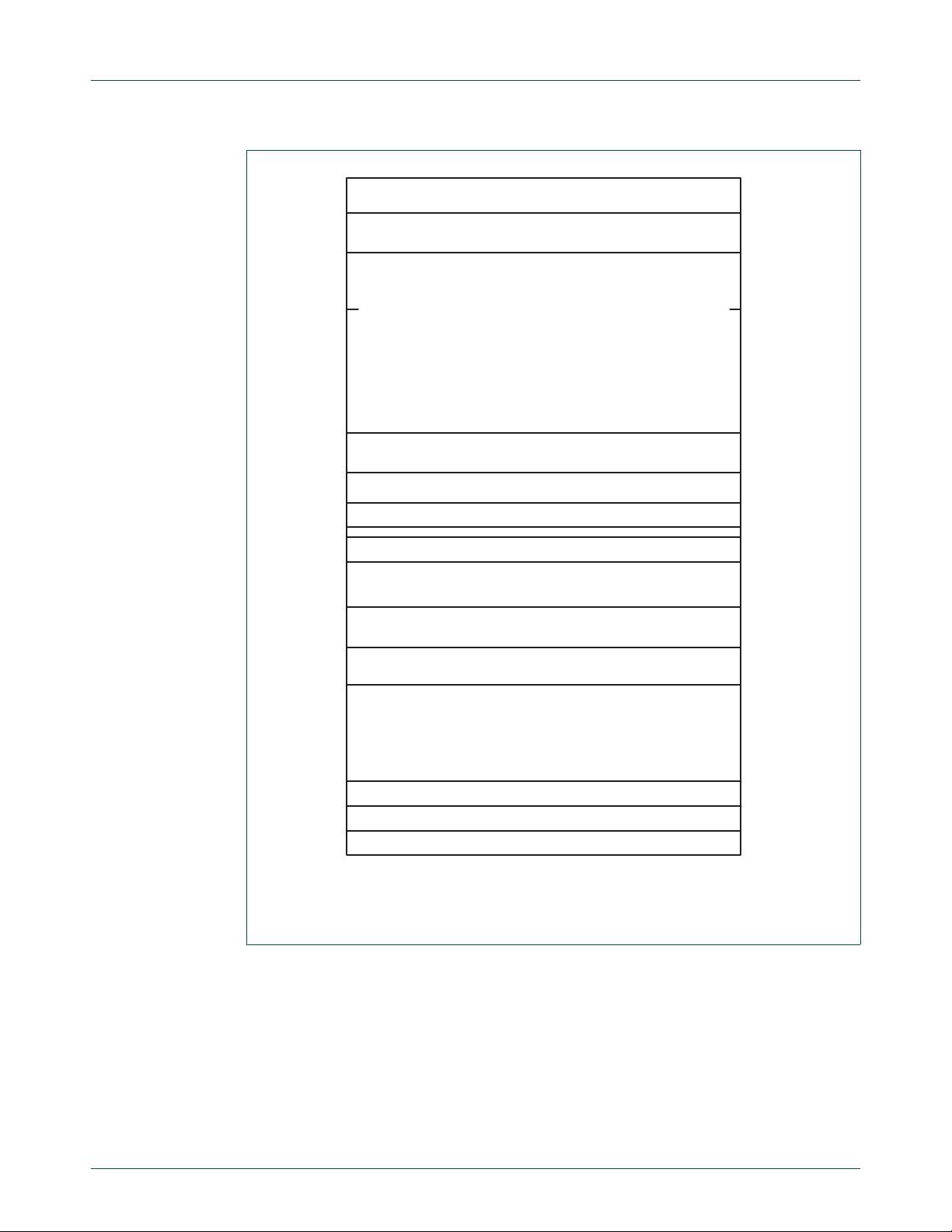
PWM1
ARM7TDMI-S
PLL
EINT3 to EINT0
FLASH
P3, P4
P0, P1, P2,
LEGACY GPI/O
52 PINS TOTAL
P0, P1
SCK, SCK0
MOSI, MOSI0
SSEL, SSEL0
SCK1
MOSI1
MISO1
SSEL1
SCL0, SCL1, SCL2
I2SRX_CLK
I2STX_CLK
I2SRX_WS
I2STX_WS
6 × AD0
RTCX1
RTCX2
RXD0, RXD2, RXD3
TXD1
RXD1
RD1, RD2
TD1, TD2
CAN1, CAN2
USB port 1
XTAL1
TCK TDO
EXTIN0
XTAL2
RESET
TRST
TDITMS
HIGH-SPEED
GPI/O
70 PINS
TOTAL
LPC2361/62
8/32 kB
SRAM
64/128 kB
FLASH
INTERNAL
CONTROLLERS
TEST/DEBUG
INTERFACE
EMULATION
TRACE MODULE
trace signals
AHB
BRIDGE
AHB
BRIDGE
ETHERNET
MAC WITH
DMA
(1)
16 kB
SRAM
MASTER
PORT
AHB TO
AHB BRIDGE
SLAVE
PORT
system
clock
SYSTEM
FUNCTIONS
INTERNAL RC
OSCILLATOR
V
DDA
V
DD(3V3)
VREF
V
SSA
, V
SS
VECTORED
INTERRUPT
CONTROLLER
8 kB
SRAM
USB WITH
4 kB RAM
AND DMA
GP DMA
CONTROLLER
I2S INTERFACE
SPI, SSP0 INTERFACE
I2SRX_SDA
I2STX_SDA
MISO, MISO0
SSP1 INTERFACE
TXD0, TXD2, TXD3
UART0, UART2, UART3
UART1
DTR1, RTS1
DSR1, CTS1, DCD1,
RI1
I
2
C0, I2C1, I2C2
SDA0, SDA1, SDA2
EXTERNAL INTERRUPTS
CAPTURE/COMPARE
TIMER0/TIMER1/
TIMER2/TIMER3
A/D CONVERTER
D/A CONVERTER
2 kB BATTERY RAM
RTC
OSCILLATOR
REAL-
TIME
CLOCK
WATCHDOG TIMER
SYSTEM CONTROL
2 × CAP0/CAP1/
CAP2/CAP3
4 × MAT2,
2 × MAT0/MAT1/
MAT3
6 × PWM1
2 × PCAP1
AOUT
VBAT
AHB TO
APB BRIDGE
SRAM
RMII(8)
V
BUS
002aad964
P0, P2
power domain 2
AHB2
AHB1
power domain 2
V
DD(DCDC)(3V3)
NXP Semiconductors
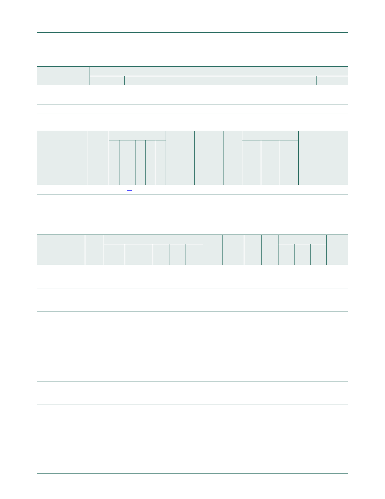
10. Block diagram
UM10211
Chapter 1: LPC23XX Introductory information
(1) LPC2362 only.
Fig 1. LPC2361/62 block diagram
UM10211_1 © NXP B.V. 2009. All rights reserved.
User manual Rev. 02 — 11 February 2009 11 of 706
Page 12
PWM1
ARM7TDMI-S
PLL
EINT3 to EINT0
FLASH
P3, P4
P0, P1, P2,
LEGACY GPI/O
52 PINS TOTAL
P0, P1
SCK, SCK0
MOSI, MOSI0
SSEL, SSEL0
SCK1
MOSI1
MISO1
SSEL1
SCL0, SCL1, SCL2
I2SRX_CLK
I2STX_CLK
I2SRX_WS
I2STX_WS
6 × AD0
RTCX1
RTCX2
MCICLK, MCIPWR
RXD0, RXD2, RXD3
TXD1
RXD1
RD1, RD2
TD1, TD2
CAN1, CAN2
(2)
USB_D+, USB_D−
XTAL1
TCK TDO
EXTIN0
XTAL2
RESET
TRST
TDITMS
HIGH-SPEED
GPI/O
70 PINS
TOTAL
LPC2364/65/66/67/68
8/32 kB
SRAM
128/256/
512 kB
FLASH
INTERNAL
CONTROLLERS
TEST/DEBUG
INTERFACE
EMULATION
TRACE MODULE
trace signals
AHB
BRIDGE
AHB
BRIDGE
ETHERNET
MAC WITH
DMA
16 kB
SRAM
MASTER
PORT
AHB TO
AHB BRIDGE
SLAVE
PORT
system
clock
SYSTEM
FUNCTIONS
INTERNAL RC
OSCILLATOR
V
DDA
V
DD(3V3)
VREF
V
SSA
, V
SS
VECTORED
INTERRUPT
CONTROLLER
8 kB
SRAM
USB WITH
4 kB RAM
AND DMA
(2)
GP DMA
CONTROLLER
I2S INTERFACE
SPI, SSP0 INTERFACE
I2SRX_SDA
I2STX_SDA
MISO, MISO0
SSP1 INTERFACE
SD/MMC CARD
INTERFACE
(1)
MCICMD,
MCIDAT[3:0]
TXD0, TXD2, TXD3
UART0, UART2, UART3
UART1
DTR1, RTS1
DSR1, CTS1, DCD1,
RI1
I
2
C0, I2C1, I2C2
SDA0, SDA1, SDA2
EXTERNAL INTERRUPTS
CAPTURE/COMPARE
TIMER0/TIMER1/
TIMER2/TIMER3
A/D CONVERTER
D/A CONVERTER
2 kB BATTERY RAM
RTC
OSCILLATOR
REAL-
TIME
CLOCK
WATCHDOG TIMER
SYSTEM CONTROL
2 × CAP0/CAP1/
CAP2/CAP3
4 × MAT2,
2 × MAT0/MAT1/
MAT3
6 × PWM1
2 × PCAP1
AOUT
VBAT
AHB TO
APB BRIDGE
SRAM
RMII(8)
V
BUS
USB_CONNECT
USB_UP_LED
002aac566
P0, P2
power domain 2
AHB2
AHB1
power domain 2
V
DD(DCDC)(3V3)
NXP Semiconductors
UM10211
Chapter 1: LPC23XX Introductory information
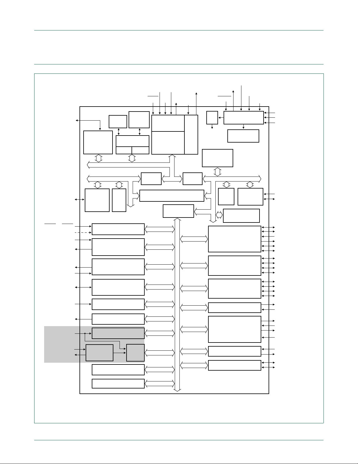
(1) LPC2367/68 only.
(2) LPC2364/66/68 only.
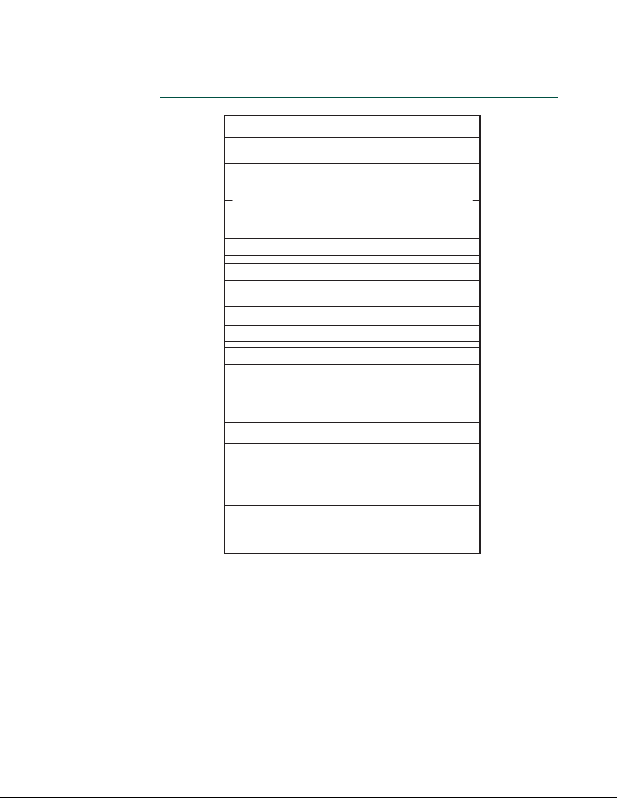
Fig 2. LPC2364/65/66/67/68 block diagram
UM10211_1 © NXP B.V. 2009. All rights reserved.
User manual Rev. 02 — 11 February 2009 12 of 706
Page 13

NXP Semiconductors
power domain 2
LPC2377/78
A[15:0]
D[7:0]
EXTERNAL
MEMORY
CONTROLLER
ALARM
002aac574
PWM1
ARM7TDMI-S
PLL
EINT3 to EINT0
FLASH
P3, P4
P0, P1, P2,
LEGACY GPI/O
56 PINS TOTAL
P0, P1
SCK, SCK0
MOSI, MOSI0
SSEL, SSEL0
SCK1
MOSI1
MISO1
SSEL1
SCL0, SCL1, SCL2
I2SRX_CLK
I2STX_CLK
I2SRX_WS
I2STX_WS
8 × AD0
RTCX1
RTCX2
MCICLK, MCIPWR
RXD0, RXD2, RXD3
TXD1
RXD1
RD1, RD2
TD1, TD2
CAN1, CAN2
(1)
2 × USB_D+/USB_D−
XTAL1
TCK TDO
EXTIN0
XTAL2
TRST
TDITMS
HIGH-SPEED
GPI/O
104 PINS
TOTAL
32 kB
SRAM
512 kB
FLASH
INTERNAL
CONTROLLERS
TEST/DEBUG
INTERFACE
EMULATION
TRACE MODULE
trace signals
AHB
BRIDGE
AHB
BRIDGE
ETHERNET
MAC WITH
DMA
16 kB
SRAM
MASTER
PORT
AHB TO
AHB BRIDGE
SLAVE
PORT
system
clock
SYSTEM
FUNCTIONS
INTERNAL RC
OSCILLATOR
V
DDA
V
DD(3V3)
V
DD(DCDC)(3V3)
VREF
V
SSA
, V
SS
VECTORED
INTERRUPT
CONTROLLER
8 kB
SRAM
USB WITH
4 kB RAM
AND DMA
(1)
GP DMA
CONTROLLER
I2S INTERFACE
SPI, SSP0 INTERFACE
I2SRX_SDA
I2STX_SDA
MISO, MISO0
SSP1 INTERFACE
SD/MMC CARD
INTERFACE
MCICMD,
MCIDAT[3:0]
TXD0, TXD2, TXD3
UART0, UART2, UART3
UART1
DTR1, RTS1
DSR1, CTS1, DCD1,
RI1
I
2
C0, I2C1, I2C2
SDA0, SDA1, SDA2
EXTERNAL INTERRUPTS
CAPTURE/COMPARE
TIMER0/TIMER1/
TIMER2/TIMER3
A/D CONVERTER
D/A CONVERTER
2 kB BATTERY RAM
RTC
OSCILLATOR
REAL-
TIME
CLOCK
WATCHDOG TIMER
SYSTEM CONTROL
2 × CAP0/CAP1/
CAP2/CAP3
4 × MAT2,
2 × MAT0/MAT1/
MAT3
6 × PWM1
2 × PCAP1
AOUT
VBAT
AHB TO
APB BRIDGE
SRAM
RMII(8)
RESET
V
BUS
2 × USB_CONNECT
2 × USB_UP_LED
DBGEN
P0, P2
AHB2 AHB1
OE, CS0, CS1,
BLS0
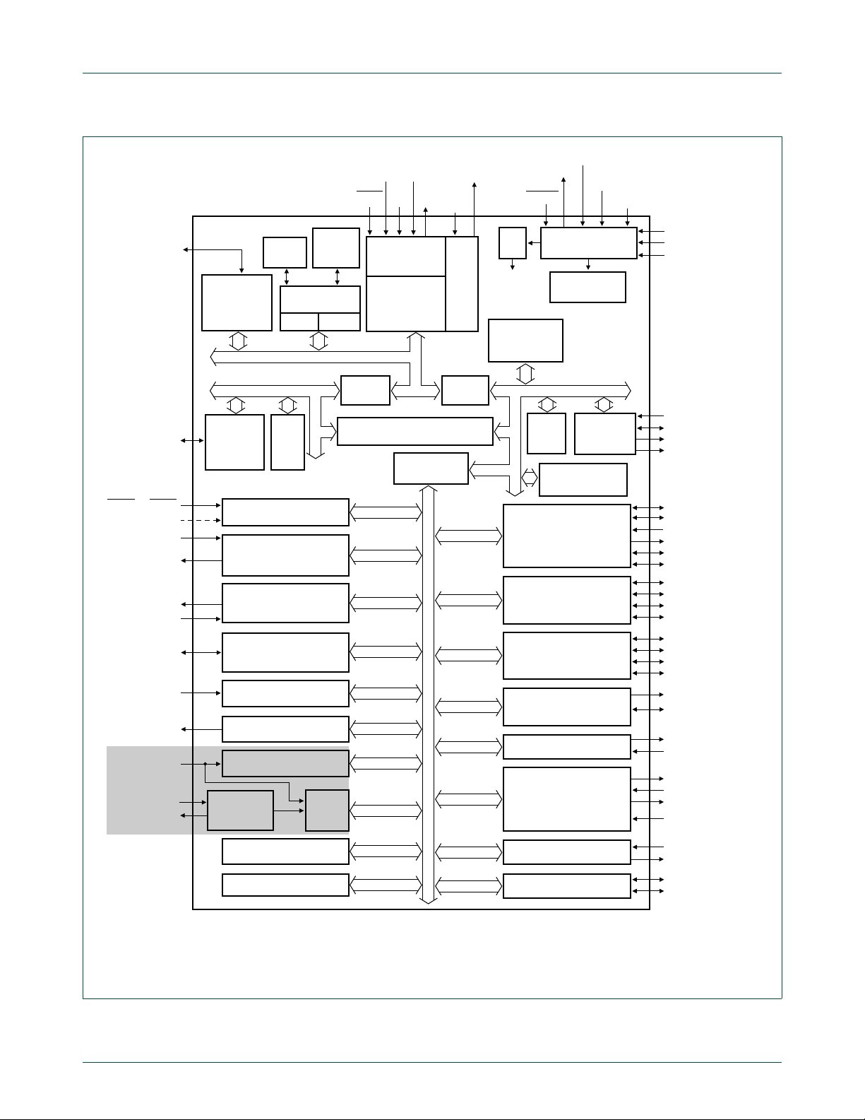
UM10211
Chapter 1: LPC23XX Introductory information
(1) LPC2378 only.
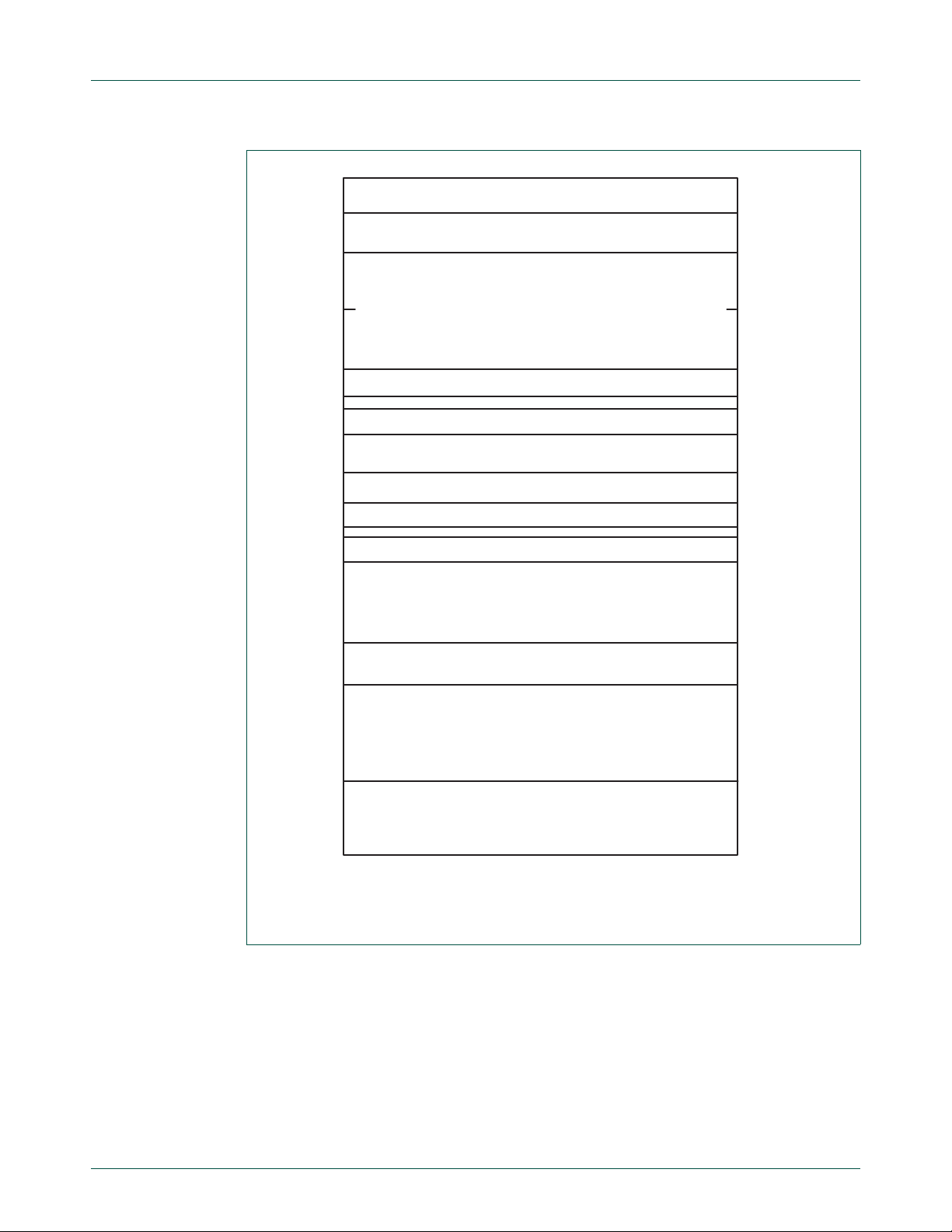
Fig 3. LPC2377/78 block diagram
UM10211_1 © NXP B.V. 2009. All rights reserved.
User manual Rev. 02 — 11 February 2009 13 of 706
Page 14

PWM1
ARM7TDMI-S
PLL
EINT3 to EINT0
FLASH
P3, P4
P0, P1, P2,
LEGACY GPI/O
52 PINS TOTAL
P0, P1
SCK, SCK0
MOSI, MOSI0
SSEL, SSEL0
SCK1
MOSI1
MISO1
SSEL1
SCL0, SCL1, SCL2
I2SRX_CLK
I2STX_CLK
I2SRX_WS
I2STX_WS
6 × AD0
RTCX1
RTCX2
MCICLK, MCIPWR
RXD0, RXD2, RXD3
TXD1
RXD1
RD1, RD2
TD1, TD2
CAN1, CAN2
USB port 1
XTAL1
TCK TDO
EXTIN0
XTAL2
RESET
TRST
TDITMS
HIGH-SPEED
GPIO
70 PINS
TOTAL
LPC2387
64 kB
SRAM
512 kB
FLASH
INTERNAL
CONTROLLERS
TEST/DEBUG
INTERFACE
EMULATION
TRACE MODULE
trace signals
AHB
BRIDGE
AHB
BRIDGE
ETHERNET
MAC WITH
DMA
16 kB
SRAM
MASTER
PORT
AHB TO
AHB BRIDGE
SLAVE
PORT
system
clock
SYSTEM
FUNCTIONS
INTERNAL RC
OSCILLATOR
V
DDA
V
DD(3V3)
VREF
V
SSA
, V
SS
VECTORED
INTERRUPT
CONTROLLER
16 kB
SRAM
USB WITH
4 kB RAM
AND DMA
GP DMA
CONTROLLER
I2S INTERFACE
SPI, SSP0 INTERFACE
I2SRX_SDA
I2STX_SDA
MISO, MISO0
SSP1 INTERFACE
SD/MMC CARD
INTERFACE
MCICMD,
MCIDAT[3:0]
TXD0, TXD2, TXD3
UART0, UART2, UART3
UART1
DTR1, RTS1
DSR1, CTS1, DCD1,
RI1
I
2
C0, I2C1, I2C2
SDA0, SDA1, SDA2
EXTERNAL INTERRUPTS
CAPTURE/COMPARE
TIMER0/TIMER1/
TIMER2/TIMER3
A/D CONVERTER
D/A CONVERTER
2 kB BATTERY RAM
RTC
OSCILLATOR
REAL-
TIME
CLOCK
WATCHDOG TIMER
SYSTEM CONTROL
2 × CAP0/CAP1/
CAP2/CAP3
4 × MAT2,
2 × MAT0/MAT1/
MAT3
6 × PWM1
2 × PCAP1
AOUT
VBAT
AHB TO
APB BRIDGE
SRAM
RMII(8)
V
BUS
002aad328
P0, P2
power domain 2
AHB2
AHB1
power domain 2
V
DD(DCDC)(3V3)
NXP Semiconductors
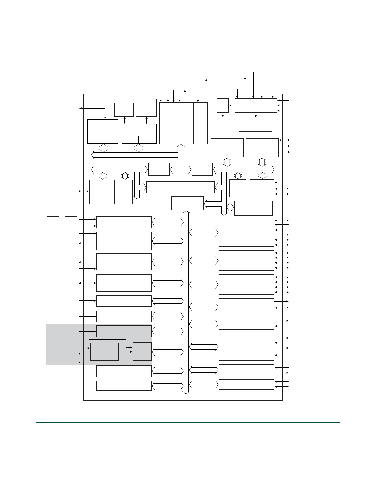
UM10211
Chapter 1: LPC23XX Introductory information
Fig 4. LPC2387 block diagram
UM10211_1 © NXP B.V. 2009. All rights reserved.
User manual Rev. 02 — 11 February 2009 14 of 706
Page 15
PWM1
ARM7TDMI-S
PLL
EINT3 to EINT0
FLASH
P3, P4
P0, P1, P2,
LEGACY GPI/O
56 PINS TOTAL
P0, P1
SCK, SCK0
MOSI, MOSI0
SSEL, SSEL0
SCK1
MOSI1
MISO1
SSEL1
SCL0, SCL1, SCL2
I2SRX_CLK
I2STX_CLK
I2SRX_WS
I2STX_WS
8 × AD0
RTCX1
RTCX2
MCICLK, MCIPWR
RXD0, RXD2, RXD3
TXD1
RXD1
RD1, RD2
TD1, TD2
CAN1, CAN2
USB port 1
XTAL1
TCK TDO
EXTIN0
XTAL2
RESET
TRST
TDITMS
HIGH-SPEED
GPI/O
104 PINS
TOTAL
LPC2388
USB port 2
64 kB
SRAM
512 kB
FLASH
INTERNAL
CONTROLLERS
TEST/DEBUG
INTERFACE
EMULATION
TRACE MODULE
trace signals
AHB
BRIDGE
AHB
BRIDGE
ETHERNET
MAC WITH
DMA
16 kB
SRAM
MASTER
PORT
AHB TO
AHB BRIDGE
SLAVE
PORT
system
clock
SYSTEM
FUNCTIONS
INTERNAL RC
OSCILLATOR
V
DDA
V
DD(3V3)
VREF
V
SSA
, V
SS
VECTORED
INTERRUPT
CONTROLLER
16 kB
SRAM
USB WITH
4 kB RAM
AND DMA
GP DMA
CONTROLLER
I2S INTERFACE
SPI, SSP0 INTERFACE
I2SRX_SDA
I2STX_SDA
MISO, MISO0
SSP1 INTERFACE
SD/MMC CARD
INTERFACE
MCICMD,
MCIDAT[3:0]
TXD0, TXD2, TXD3
UART0, UART2, UART3
UART1
DTR1, RTS1
DSR1, CTS1, DCD1,
RI1
I
2
C0, I2C1, I2C2
SDA0, SDA1, SDA2
EXTERNAL INTERRUPTS
CAPTURE/COMPARE
TIMER0/TIMER1/
TIMER2/TIMER3
A/D CONVERTER
D/A CONVERTER
2 kB BATTERY RAM
RTC
OSCILLATOR
REAL-
TIME
CLOCK
WATCHDOG TIMER
SYSTEM CONTROL
2 × CAP0/CAP1/
CAP2/CAP3
4 × MAT2,
2 × MAT0/MAT1/
MAT3
6 × PWM1
2 × PCAP1
AOUT
VBAT
AHB TO
APB BRIDGE
SRAM
RMII(8)
V
BUS
002aad332
P0, P2
power domain 2
AHB2
AHB1
power domain 2
V
DD(DCDC)(3V3)
A[15:0]
D[7:0]
EXTERNAL
MEMORY
CONTROLLER
OE, CS0, CS1,
BLS0
ALARM
NXP Semiconductors
UM10211
Chapter 1: LPC23XX Introductory information
Fig 5. LPC2388 block diagram
UM10211_1 © NXP B.V. 2009. All rights reserved.
User manual Rev. 02 — 11 February 2009 15 of 706
Page 16

UM10211
Chapter 2: LPC23XX memory addressing
Rev. 02 — 11 February 2009 User manual
1. Memory map and peripheral addressing
ARM processors have a single 4 GB address space. The following table shows how this
space is used on NXP embedded ARM devices. For memory option det ails see Table 1–2
Table 9. LPC2300 memory usage
Address range General use Address range details and description
0x0000 0000 to
0x3FFF FFFF
0x4000 0000 to
0x7FFF FFFF
0x8000 0000 to
0xDFFF FFFF
0xE000 0000 to
0xEFFF FFFF
0xF000 0000 to
0xFFFF FFFF
on-chip
NV memory
and fast I/O
on-chip RAM 0x4000 0000 - 0x4000 7FFF RAM (up to 32 kB)
off-chip memory Two static memory banks, 64 KB each (LPC2377/78 and LPC2388 only):
APB peripherals 0xE000 0000 - 0xE008 FFFF 36 peripheral blocks, 16 kB each (some unused),
AHB peripherals 0xFFE0 0000 - 0xFFE0 3FFF Ethernet Controller (not LPC2361)
0x0000 0000 - 0x0007 FFFF flash memory (up to 512 kB)
0x3FFF C000 - 0x3FFF FFF F fast GPIO registers
0x4000 0000 - 0x4000 FFFF RAM (64 kB for LPC2387/88)
0x7FD0 0000 - 0x7FD0 1FFF USB RAM (8 kB)
0x7FD0 0000 - 0x7FD0 3FFF USB RAM (16 kB for LPC2387/88)
0x7FE0 0000 - 0x7FE0 3FFF Ethernet RAM (16 kB)
0x8000 0000 - 0x8000 FFFF static memory bank 0, 64 KB
0x8100 0000 - 0x8100 FFFF static memory bank 1, 64 KB
see Table 2–10
0xE01F C000 - 0xE01F FFFF System Control Block
0xFFE0 4000 - 0xFFE0 7FFF General Purpose DMA Controller
0xFFE0 8000 - 0xFFE0 BFFF External Memory Controller (EMC) (LPC2377/78,
LPC2388 only)
0xFFE0 C000 - 0xFFE0 FFFF USB Controller (LPC2361/62/64/66/68, LPC2378,
LPC2387, and LPC2388 only).
0xFFFF F000 - 0xFFFF FFFF Vectored Interrupt Controller (VIC)
.
.
2. Memory maps
The LPC2300 incorporates several distinct memory regions, shown in the following
figures. Figure 2–7
address space from the user program viewpoint following reset. Th e interrupt vector area
supports address remapping, which is described later in this section.
UM10211_2 © NXP B.V. 2009. All rights reserved.
User manual Rev. 02 — 11 February 2009 16 of 706
, Figure 2–8, and Figure 2–9 show the overall map of the entire
Page 17

NXP Semiconductors
0.0 GB
1.0 GB
TOTAL OF 64 kB ON-CHIP NON-VOLATILE MEMORY (LPC2361)
TOTAL OF 128 kB ON-CHIP NON-VOLATILE MEMORY (LPC2362)
0x0000 0000
0x0000 FFFF
0x0001 0000
0x0001 FFFF
0x0002 0000
RESERVED FOR ON-CHIP MEMORY
8 kB LOCAL ON-CHIP STATIC RAM (LPC2361)
32 kB LOCAL ON-CHIP STATIC RAM (LPC2362)
RESERVED ADDRESS SPACE
RESERVED ADDRESS SPACE
0x4000 0000
0x4000 2000
0x4000 8000
0x7FD0 0000
0x7FE0 0000
0x7FD0 1FFF
0x7FE0 3FFF
0x4000 1FFF
0x4000 7FFF
2.0 GB
0x8000 0000
BOOT ROM AND BOOT FLASH
(BOOT FLASH REMAPPED FROM ON-CHIP FLASH)
3.0 GB 0xC000 0000
RESERVED ADDRESS SPACE
3.75 GB
4.0 GB
3.5 GB
AHB PERIPHERALS
APB PERIPHERALS
0xE000 0000
0xF000 0000
0xFFFF FFFF
GENERAL PURPOSE OR USB RAM (8 KB)
ETHERNET RAM (16 kB)
002aae283
UM10211
Chapter 2: LPC23XX memory addressing
Fig 6. LPC2461/63 memory map
UM10211_2 © NXP B.V. 2009. All rights reserved.
User manual Rev. 02 — 11 February 2009 17 of 706
Page 18
NXP Semiconductors
0.0 GB
1.0 GB
TOTAL OF 128 kB ON-CHIP NON-VOLATILE MEMORY (LPC2364)
TOTAL OF 512 kB ON-CHIP NON-VOLATILE MEMORY (LPC2367/68)
TOTAL OF 256 kB ON-CHIP NON-VOLATILE MEMORY (LPC2365/66)
0x0000 0000
0x0001 FFFF
0x0002 0000
0x0003 FFFF
0x0007 FFFF
0x0008 0000
0x0004 0000
RESERVED FOR ON-CHIP MEMORY
8 kB LOCAL ON-CHIP STATIC RAM (LPC2364)
32 kB LOCAL ON-CHIP STATIC RAM (LPC2365/66/67/68)
RESERVED ADDRESS SPACE
RESERVED ADDRESS SPACE
0x4000 0000
0x4000 2000
0x4000 8000
0x7FD0 0000
0x7FE0 0000
0x7FD0 1FFF
0x7FE0 3FFF
0x4000 1FFF
0x4000 7FFF
2.0 GB
0x8000 0000
BOOT ROM AND BOOT FLASH
(BOOT FLASH REMAPPED FROM ON-CHIP FLASH)
3.0 GB 0xC000 0000
RESERVED ADDRESS SPACE
3.75 GB
4.0 GB
3.5 GB
AHB PERIPHERALS
APB PERIPHERALS
0xE000 0000
0xF000 0000
0xFFFF FFFF
GENERAL PURPOSE OR USB RAM (8 KB)
ETHERNET RAM (16 kB)
002aac577
UM10211
Chapter 2: LPC23XX memory addressing
Fig 7. LPC2364/65/66/67/68 system mem ory map
UM10211_2 © NXP B.V. 2009. All rights reserved.
User manual Rev. 02 — 11 February 2009 18 of 706
Page 19
NXP Semiconductors
0.0 GB
1.0 GB
TOTAL OF 512 kB ON-CHIP NON-VOLATILE MEMORY
0x0000 0000
0x0007 FFFF
0x0008 0000
RESERVED ADDRESS SPACE
32 kB LOCAL ON-CHIP STATIC RAM
RESERVED ADDRESS SPACE
RESERVED ADDRESS SPACE
0x4000 0000
0x4000 8000
0x7FD0 0000
0x7FE0 0000
0x7FD0 1FFF
0x7FE0 3FFF
0x4000 7FFF
2.0 GB
0x8000 0000
0x8000 FFFF
0x8100 FFFF
0x8100 0000
BOOT ROM AND BOOT FLASH
(BOOT FLASH REMAPPED FROM ON-CHIP FLASH)
3.0 GB 0xC000 0000
RESERVED ADDRESS SPACE
3.75 GB
4.0 GB
3.5 GB
AHB PERIPHERALS
APB PERIPHERALS
0xE000 0000
0xF000 0000
0xFFFF FFFF
GENERAL PURPOSE OR USB RAM (8 kB)
ETHERNET RAM (16 kB)
002aac585
EXTERNAL MEMORY BANK 0 (64 kB)
EXTERNAL MEMORY BANK 1 (64 kB)
UM10211
Chapter 2: LPC23XX memory addressing
Fig 8. LPC2377/78 system memory map
UM10211_2 © NXP B.V. 2009. All rights reserved.
User manual Rev. 02 — 11 February 2009 19 of 706
Page 20

NXP Semiconductors
0.0 GB
1.0 GB
TOTAL OF 512 kB ON-CHIP NON-VOLATILE MEMORY
0x0000 0000
0x0007 FFFF
0x0008 0000
RESERVED FOR ON-CHIP MEMORY
64 kB LOCAL ON-CHIP STATIC RAM
RESERVED ADDRESS SPACE
RESERVED ADDRESS SPACE
0x4000 0000
0x4001 0000
0x7FD0 0000
0x7FE0 0000
0x7FD0 3FFF
0x7FE0 3FFF
0x4000 FFFF
2.0 GB
BOOT ROM AND BOOT FLASH
(BOOT FLASH REMAPPED FROM ON-CHIP FLASH)
3.0 GB 0xC000 0000
RESERVED ADDRESS SPACE
3.75 GB
4.0 GB
3.5 GB
AHB PERIPHERALS
APB PERIPHERALS
0xE000 0000
0xF000 0000
0xFFFF FFFF
USB RAM (16 kB)
ETHERNET RAM (16 kB)
002aad331
0x8000 0000
0x8000 FFFF
0x8100 FFFF
0x8100 0000
EXTERNAL MEMORY BANK 0 (64 kB)
EXTERNAL MEMORY BANK 1 (64 kB)
UM10211
Chapter 2: LPC23XX memory addressing
Fig 9. LPC2387 memory map
UM10211_2 © NXP B.V. 2009. All rights reserved.
User manual Rev. 02 — 11 February 2009 20 of 706
Page 21
NXP Semiconductors
0.0 GB
1.0 GB
TOTAL OF 512 kB ON-CHIP NON-VOLATILE MEMORY
0x0000 0000
0x0007 FFFF
0x0008 0000
RESERVED FOR ON-CHIP MEMORY
64 kB LOCAL ON-CHIP STATIC RAM
RESERVED ADDRESS SPACE
RESERVED ADDRESS SPACE
0x4000 0000
0x4001 0000
0x7FD0 0000
0x7FE0 0000
0x7FD0 3FFF
0x7FE0 3FFF
0x4000 FFFF
2.0 GB
BOOT ROM AND BOOT FLASH
(BOOT FLASH REMAPPED FROM ON-CHIP FLASH)
3.0 GB 0xC000 0000
RESERVED ADDRESS SPACE
3.75 GB
4.0 GB
3.5 GB
AHB PERIPHERALS
APB PERIPHERALS
0xE000 0000
0xF000 0000
0xFFFF FFFF
USB RAM (16 kB)
ETHERNET RAM (16 kB)
002aad331
0x8000 0000
0x8000 FFFF
0x8100 FFFF
0x8100 0000
EXTERNAL MEMORY BANK 0 (64 kB)
EXTERNAL MEMORY BANK 1 (64 kB)
UM10211
Chapter 2: LPC23XX memory addressing
Fig 10. LPC2388 memory map
UM10211_2 © NXP B.V. 2009. All rights reserved.
User manual Rev. 02 — 11 February 2009 21 of 706
Page 22

NXP Semiconductors
RESERVED
RESERVED
0xF000 0000
0xEFFF FFFF
APB PERIPHERALS
0xE020 0000
0xE01F FFFF
0xE000 0000
AHB PERIPHERALS
0xFFFF FFFF
0xFFE0 0000
0xFFDF FFFF
3.75 GB
3.5 GB
3.5 GB + 2 MB
4.0 GB - 2 MB
4.0 GB
UM10211
Chapter 2: LPC23XX memory addressing
Fig 11. Peripheral memory map
Figure 12 and Table 2–10 show different views of the peripheral address space. Both the
AHB and APB peripheral areas are 2 megabyte spaces which are divided up into 128
peripherals. Each peripheral space is 16 kilobytes in size. This allows simplifying the
address decoding for each peripheral.
UM10211_2 © NXP B.V. 2009. All rights reserved.
User manual Rev. 02 — 11 February 2009 22 of 706
Page 23
NXP Semiconductors
VECTORED INTERRUPT CONTROLLER
(AHB PERIPHERAL #0)
0xFFFF F000 (4G - 4K)
0xFFFF C000
0xFFFF 8000
(AHB PERIPHERAL #4)
(AHB PERIPHERAL #3)
(AHB PERIPHERAL #2)
(AHB PERIPHERAL #1)
(AHB PERIPHERAL #126)
0xFFE1 8000
0xFFE1 4000
0xFFE1 0000
0xFFE0 C000
0xFFE0 8000
0xFFE0 4000
0xFFE0 0000
ETHERNET CONTROLLER
GENERAL PURPOSE DMA CONTROLLER
EXTERNAL MEMORY CONTROLLER
USB CONTROLLER
NOT USED
(AHB PERIPHERAL #5)
NOT USED
All peripheral register addresses are word aligned (to 32 bit boundaries) regardless of
their size. This eliminates the need for byte lane mapping hardware that would be required
to allow byte (8 bit) or half-word (16 bit) accesses to occur at smaller boundaries. An
implication of this is that word and half-word registers must be accessed all at once. For
example, it is not possible to read or write the upper byte of a word register separately.
UM10211
Chapter 2: LPC23XX memory addressing
UM10211_2 © NXP B.V. 2009. All rights reserved.
User manual Rev. 02 — 11 February 2009 23 of 706
Fig 12. AHB peripheral map
Page 24

NXP Semiconductors
3. APB peripheral addresses
The following table shows the APB address map. No APB peripheral uses all of the 16 kB
space allocated to it. T ypically each device’ s registers are "aliased" or re peated at multiple
locations within each 16 kB range.
Table 10. APB peripherals and base addresses
APB Peripheral Base Address Peripheral Name
0 0xE000 0000 Watchdog Timer
1 0xE000 4000 Timer 0
2 0xE000 8000 Timer 1
3 0xE000 C000 UART0
4 0xE001 0000 UART1
5 0xE001 4000 Not used
6 0xE001 8000 PWM1
7 0xE001 C000 I
8 0xE002 0000 SPI
9 0xE002 4000 RTC
10 0xE002 8000 GPIO
1 1 0xE002 C000 Pin Connect Block
12 0xE003 0000 SSP1
13 0xE003 4000 ADC
14 0xE003 8000 CAN Acceptance Filter RAM
15 0xE003 C000 CAN Acceptance Filter Registers
16 0xE004 0000 CAN Common Registers
17 0xE004 4000 CAN Controller 1
18 0xE004 8000 CAN Controller 2
19 to 22 0xE004 C000 to 0xE005 8000 Not used
23 0xE005 C000 I
24 0xE006 0000 Not used
25 0xE006 4000 Not used
26 0xE006 8000 SSP0
27 0xE006 C000 DAC
28 0xE007 0000 Timer 2
29 0xE007 4000 Timer 3
30 0xE007 8000 UART2
31 0xE007 C000 UART3
32 0xE008 0000 I
33 0xE008 4000 Battery RAM
34 0xE008 8000 I2S
35 0xE008 C000 SD/MMC Card Interface
36 to 126 0xE009 0000 to 0xE01F BFFF Not used
127 0xE01F C000 System Control Block
UM10211
Chapter 2: LPC23XX memory addressing
2
C0
[1]
[1]
[1]
[1]
[1]
2
C1
2
C2
[2]
[1] CAN interface is available in LPC2364/66/68, LPC2378, LPC2387, and LPC2388.
UM10211_2 © NXP B.V. 2009. All rights reserved.
User manual Rev. 02 — 11 February 2009 24 of 706
Page 25

NXP Semiconductors
Chapter 2: LPC23XX memory addressing
[2] The SD/MMC card interface is available in LPC2365/66, LPC2377/78, LPC2387, and LPC2388.
4. LPC2300 memory re-mapping and boot ROM
4.1 Memory map concepts and operating modes
The basic concept on the LPC2300 is that each memory area has a "natural" location in
the memory map. This is the address range for which code residing in that area is written.
The bulk of each memory space remains permanently fixed in the same location,
eliminating the need to have portions of the code designed to run in different address
ranges.
Because of the location of the interrupt vectors on the ARM7 processor (at addresses
0x0000 0000 through 0x0000 001C, as shown in Table 2–11
Boot ROM and SRAM spaces need to be re-mapped in order to allow alternative uses of
interrupts in the differen t operating modes described in Table 2–12
interrupts is accomplished via the Memory Mapping Contro l feature (Section 2–5 “
mapping control” on page 27).
Table 11. ARM exception vector locations
Address Exception
0x0000 0000 Reset
0x0000 0004 Undefined Instruction
0x0000 0008 Software Interrupt
0x0000 000C Prefetch Abort (instruction fetch memory fault)
0x0000 0010 Data Abort (data access memory fault)
0x0000 0014 Reserved
UM10211
below), a small portion of the
. Re-mapping of the
Memory
Note: Identified as reserved in ARM documentation, this location is used
by the Boot Loader as the Valid User Program key. This is described in
detail in Section 29–3.1.1
0x0000 0018 IRQ
0x0000 001C FIQ
Table 12. LPC2300 Memory mapping modes
Mode Activation Usage
Boot
Loader
mode
UM10211_2 © NXP B.V. 2009. All rights reserved.
User manual Rev. 02 — 11 February 2009 25 of 706
Hardware
activation by
any Reset
The Boot Loader always executes after any reset. The Boot ROM
interrupt vectors are mapped to the bottom of memory to allow
handling exceptions and using interrupts during the Boot Loading
process. A sector of the Flash memory (the Boot Flash) is available to
hold part of the Boot Code.
.
Page 26

NXP Semiconductors
Table 12. LPC2300 Memory mapping modes
Mode Activation Usage
User
Flash
mode
User RAM
mode
User
External
Memory
mode
[1] See EMCControl register address mirror bit in Table5–60 for address of external memory bank 0.
4.2 Memory re-mapping
In order to allow for compatibility with future derivatives, the entire Boot ROM is mapped
to the top of the on-chip memory space. In this manner, the use of larger or smaller flash
modules will not require changing the location of the Boot ROM (which would require
changing the Boot Loader code itself) or changing the mapping of the Boot ROM interru pt
vectors. Memory spaces other than the interrupt vectors remain in fixed locations.
Figure 2–13
UM10211
Chapter 2: LPC23XX memory addressing
Software
activation by
boot code
Software
activation by
user program
Software
activation by
user code
shows the on-chip memory mapping in the modes defined above.
Activated by the Boot Loader when a valid User Program Signature is
recognized in memory and Boot Loader operation is not forced.
Interrupt vectors are not re-mapped and are found in the bottom of the
Flash memory.
Activated by a User Program as desired. Interrupt vectors are
re-mapped to the bottom of the Static RAM.
Activated by a User Program as desired. Interrupt vectors are
re-mapped to external memory bank 0
[1]
.
The portion of memory that is re-mapped to allow interrupt processing in different modes
includes the interrupt vector area (32 bytes) and an additional 32 bytes for a total of
64 bytes, that facilitates branching to interrupt handlers at distant physical addresses. The
remapped code locations overlay addresses 0x0000 0000 through 0x0000 003F. A typical
user program in the Flash memory can place the entire FIQ handler at address
0x0000 001C without any need to consider mem or y bo un d ar ies. The vector contained in
the SRAM, external memory , and Boot ROM must cont ain branches to the actual interrupt
handlers, or to other instructions that accomplish the branch to the interrupt hand lers.
There are three reasons this configuration was chosen:
1. To give the FIQ handler in the Flash memory the advantage of not having to take a
memory boundary caused by the remapping into account.
2. Minimize the need to for the SRAM and Boot ROM vectors to deal with arbitrary
boundaries in the middle of code space.
3. To provide space to store constants for jumping beyond the range of single word
branch instructions.
Re-mapped memory areas, including the Boot ROM and interrupt vectors, continue to
appear in their original location in addition to the re-mapped address.
Details on re-mapping and examples can be found in Section 2–5 “
Memory mapping
control” on page 27.
UM10211_2 © NXP B.V. 2009. All rights reserved.
User manual Rev. 02 — 11 February 2009 26 of 706
Page 27

NXP Semiconductors
5. Memory mapping control
The Memory Mapping Control alters the mapping of the interrupt vectors that appear
beginning at address 0x0000 0000. This allows code running in different memory spaces
to have control of the interrupts.
5.1 Memory Mapping Control Register (MEMMAP - 0xE01F C040)
Whenever an exception handling is necessary, microcontroller will fetch an instruction
residing on exception corresponding address as described in Table 2–11 “
vector locations” on page 25. The MEMMAP register determines the source of data that
will fill this table.
Table 13. Memory mapping control registers
Name Description Access Reset
MEMMAP Memory mapping control. Selects whether the
ARM interrupt vectors are read from the Boot
ROM, User Flash, or RAM.
UM10211
Chapter 2: LPC23XX memory addressing
ARM exception
Address
value
R/W 0x00 0xE01F C040
Table 14. Memory Mapping control register (MEMMAP - address 0xE01F C040) bit
description
Bit Symbol Value Description Reset
1:0 MAP 00 Boot Loader Mode. Interrupt vectors are re-mapped to Boot ROM. 00
01 User Flash Mode. Interrupt vectors are not re-mapped and reside
in Flash.
10 User RAM Mode. Interrupt vectors are re-mapped to Static RAM.
11 User External Memory Mode (available on LPC2377/78 and
LPC2388 only).
Warning: Improper setting of this value may result in incorrect operation of
the device.
7:2 - - Reserved, user software should not write ones to reserved bits.
The value read from a reserved bit is not defined.
5.2 Memory mapping control usage notes
Memory Mapping Control simply selects one out of three available sources of data (set s of
64 bytes each) necessary for handling ARM exceptions (interrupts).
For example, whenever a Software Interrupt request is generated, ARM core will always
fetch 32 bit data "residing" on 0x0000 0008 see Table 2–11 “
locations” on page 25. This means that when MEMMAP[1:0] = 10 (User RAM Mode),
read/fetch from 0x0000 0008 will provide data stored in 0x4000 0008. In case of
MEMMAP[1:0] = 00 (Boot Loader Mode), read/fetch from 0x0000 0008 will provide data
available also at 0x7FFF E008 (Boot ROM remapped from on-chip Bootloader).
ARM exception vector
value
NA
UM10211_2 © NXP B.V. 2009. All rights reserved.
User manual Rev. 02 — 11 February 2009 27 of 706
Page 28
NXP Semiconductors
0.0 GB
0x8000 0000
0x4000 0000
0x3FFF FFFF
0x0000 0000
1.0 GB
2.0 GB - 8 kB
2.0 GB
upper limit depends on
specific part number
ACTIVE INTERRUPT VECTORS
(FROM FLASH, SRAM, BOOT ROM, OR EXT MEMORY)
BOOT FLASH
RESERVED FOR ON-CHIP MEMORY
(SRAM INTERRUPT VECTORS)
FLASH MEMORY
RESERVED FOR ON-CHIP MEMORY
(BOOT ROM INTERRUPT VECTORS)
8 kB BOOT ROM
STATIC RAM
0x7FFF FFFF
FAST GPIO REGISTERS
PARTCFG REGISTERS
0x3FFF 8000
0x3FFF C000
0x3FFF BFFF
upper limit depends on
specific part number
8 kB BOOT FLASH
(RE-MAPPED FROM TOP OF FLASH MEMORY)
EXTERNAL MEMORY INTERRUPT VECTORS
0x7FFF E000
0x7FFE FFFF
0x7FFE E000
2.0 GB - 64 kB
2.0 GB - 72 kB
UM10211
Chapter 2: LPC23XX memory addressing
Fig 13. M ap of lower memory is showing re-mapped and re-mappable areas
UM10211_2 © NXP B.V. 2009. All rights reserved.
User manual Rev. 02 — 11 February 2009 28 of 706
Page 29

NXP Semiconductors
6. Prefetch abort and data abort exceptions
The LPC2300 generates the appropriate bus cycle abort exception if an access is
attempted for an address that is in a reserved or unassigned address region. The regions
are:
• Areas of the memory map that are not implemented for a specific ARM derivative. Fo r
the LPC2300, this is:
– Address space between On-Chip Non-Volatile Memory and the Special Register
space. Labelled "Reserved for On-Chip Memory" in Figure 2–7
Figure 2–9
– Address space between On-Chip Static RAM and the Boot ROM. Labelled
"Reserved Address Space" in Figure 2–7
– External Memory
– Reserved regions of the AHB and APB spaces. See Figure 2–11
• Unassigned AHB peripheral spaces. See Figure 2–12.
• Unassigned APB peripheral spaces. See Table 2–10.
.
UM10211
Chapter 2: LPC23XX memory addressing
, Figure 2–8, and
, Figure 2–8, and Figure 2–9.
.
For these areas, both attempted data acce ss and in struction fetch genera te an exception.
In addition, a Prefetch Abort exception is generated for an y instruction fetch that maps to
an AHB or APB peripheral address, or to the Special Register space located just below
the SRAM at addresses 0x3FFF8000 through 0x3FFFFFFF.
Within the address space of an existing APB peripheral, a data abort exception is not
generated in response to an access to an undefined address. Address decoding within
each peripheral is limited to that needed to distinguish defined registers within the
peripheral itself. For example, an access to address 0xE000 D000 (an undefined addre ss
within the UART0 space) may result in an access to the register defined at address
0xE000 C000. Details of such address aliasing within a peripheral space are not defined
in the LPC2300 documentation and are not a supporte d feature.
If software executes a write directly to the Flash memory, the MAM generates a data abort
exception. Flash programming must be accomplished using the specified Flash
programming interface provided by the Boot Code.
Note that the ARM core stores the Prefetch Abort flag along with the associated
instruction (which will be meaningless) in the pipeline and processes the abort only if an
attempt is made to execute the instruction fetched from the illegal address. This prevents
accidental aborts that could be caused by prefetches that occur when code is executed
very near a memory boundary.
UM10211_2 © NXP B.V. 2009. All rights reserved.
User manual Rev. 02 — 11 February 2009 29 of 706
Page 30

1. Introduction
UM10211
Chapter 3: LPC23XX System control block
Rev. 02 — 11 February 2009 User manual
The system control block includes several system features and control registers for a
number of functions that are not related to specific peripheral devices. These include:
• Reset
• Brown-Out Detection
• External Interrupt Input s
• Miscellaneous System Controls and Status
• Code Security vs. Debugging
Each type of function has its own register(s) if any are required and unneeded bit s are
defined as reserved in order to allow future expansion. Unrelated functions never share
the same register addresses
2. Pin description
Table 3–15 shows pins that are associated with System Control block functions.
Table 15. Pin summary
Pin name Pin
EINT0 Input External Interrupt Input 0 - An active low/high level or
EINT1 Input External Interrupt Input 1 - See the EINT0 description ab ove.
EINT2 Input External Interrupt Input 2 - See the EINT0 description ab ove.
EINT3 Input External Interrupt Input 3 - See the EINT0 description ab ove.
RESET
3. Register description
All registers, regardless of size, are on word address boundaries. Details of the registers
appear in the description of each function.
T able 16. Summary of system control registers
Name Description Access Reset
External interrupts
EXTINT External Interrupt Flag Register R/W 0x00 0xE01F C140
EXTMODE External Interrupt Mode register R/W 0x00 0xE01F C148
EXTPOLAR External Interrupt Polarity Register R/W 0x00 0xE01F C14C
Pin description
direction
falling/rising edge general purpose interrupt input. This pin may be
used to wake up the processor from Idle or Power down modes.
Input External Reset input - A LOW on this pin resets the chip, causing
I/O ports and peripherals to take on their default states, and the
processor to begin execution at address 0x0000 0000.
Address
value
UM10211_2 © NXP B.V. 2009. All rights reserved.
User manual Rev. 02 — 11 February 2009 30 of 706
Page 31

NXP Semiconductors
T able 16. Summary of system control registers
Name Description Access Reset
Reset
RSID Reset Source Identification Register R/W see text 0xE01F C180
AHB configuration registers
AHBCFG1 Configures the AHB1 arbiter. R/W 0x0000
AHBCFG2 Configures the AHB2 arbiter. R/W 0x0000
Syscon miscellaneous registers
SCS System Control and Status R/W 0x00 0xE01F C1A0
4. Reset
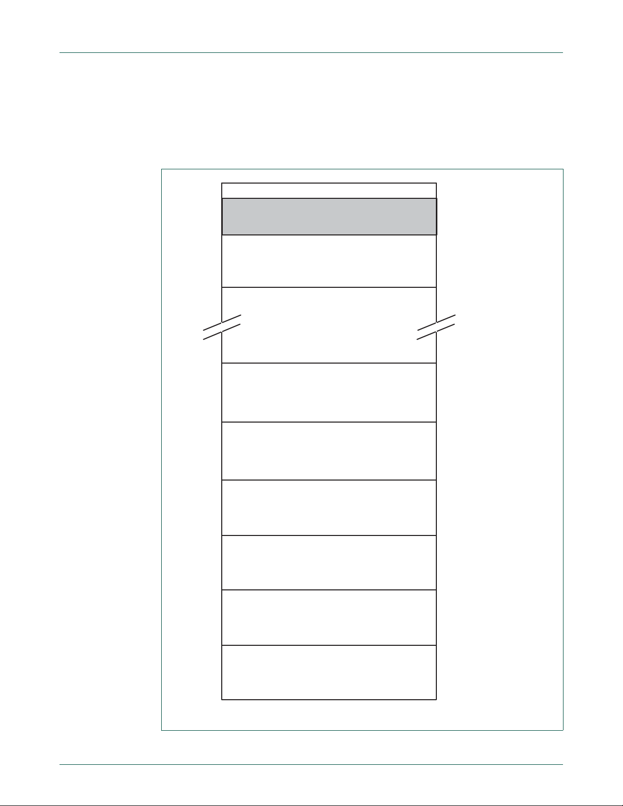
Reset has four sources on the LPC2300: the RESET pin, the Watchdog Reset, Power On
Reset (POR) and the Brown Out Detection circuit (BOD). The RESET
trigger input pin. Assertion of chip Reset by any source, once the operating volt age attains
a usable level, starts the W akeup Timer (see description in Section 4–9 “
this chapter), causing reset to remain asserted until the external Reset is de-asserted, the
oscillator is running, a fixed number of clocks have passed, and the Flash controller has
completed its initialization. The reset logic is shown in the following block diagram (see
Figure 3–14
UM10211
Chapter 3: LPC23XX System control block
Address
value
0xE01F C188
0145
0xE01F C18C
0145
pin is a Schmitt
Wakeup timer” in
).
UM10211_2 © NXP B.V. 2009. All rights reserved.
User manual Rev. 02 — 11 February 2009 31 of 706
Page 32

NXP Semiconductors
C
Q
S
APB read of
PDBIT
in PCON
power
down
C
Q
S
F
OSC
to other
blocks
WAKEUP TIMER
watchdog
reset
external
reset
START
COUNT 2
n
internal RC
oscillator
Reset to the
on-chip circuitry
Reset to
PCON.PD
write “1”
from APB
reset
EINT0 wakeup
EINT1 wakeup
EINT2 wakeup
POR
BOD
EINT3 wakeup
RTC wakeup
BOD wakeup
Ethernet MAC wakeup
USB need_clk wakeup
CAN wakeup
GPIO0 port wakeup
GPIO2 port wakeup
UM10211
Chapter 3: LPC23XX System control block
UM10211_2 © NXP B.V. 2009. All rights reserved.
User manual Rev. 02 — 11 February 2009 32 of 706
Fig 14. Reset block diagram including the wakeup timer
On the assertion of any of reset sources (POR, BOD reset, External reset and Watchdog
reset), the IRC starts up. Af ter the IRC-start-up time (maximum of 60 μs on power-up) and
after the IRC provides stable clock output, the reset signal is latched and synchronized on
the IRC clock. Then the following two sequences start simultaneously :
1. The 2-bit IRC wakeup timer starts counting when the synchronized reset is
de-asserted. The boot code in the ROM start s when the 2-bit IRC wakeup timer times
out. The boot code performs the boot tasks an d m ay jump to th e F lash. If th e Flash is
not ready to access, the MAM will insert wait cycles until the Flash is ready.
2. The Flash wakeup-timer (9-bit) starts counting when the synchronized reset is
de-asserted. The Flash wakeup-timer generates the 100 μs Flash start-up time. Once
it times out, the Flash initialization sequence is started, which takes about 250 cycles.
When it’s done, the MAM will be granted access to the Flash.
When the internal Reset is removed, the processor begins executing at address 0, which
is initially the Reset vector mapped from the Boot Block. At that point, all of the processor
and peripheral registers have been initialized to predetermined values.
Figure 3–15
processor status when the LPC2300 starts up after reset. See Section 4–4.2 “
shows an example of the relationship between the RESET, the IRC, and the
oscillator” for start-up of the main oscillator if selected by the user code.
Main
Page 33

NXP Semiconductors
valid threshold
processor status
V
DD(3V3)
IRC status
RESET
GND
002aad482
30 μs
1 μs; IRC stability count
8 μs
170 μs
160 μs
boot time user code
boot code
execution
finishes;
user code starts
flash read
finishes
flash read
starts
supply ramp-up
time
UM10211
Chapter 3: LPC23XX System control block
Fig 15. E xample of start-up after reset
The various Resets have some small dif ferences. For example, a Power On Reset causes
the value of certain pins to be latched to configure the part.
For more details on Reset, PLL and startup/boot code inte ra ction se e Section 4– 6.2 “
PLL
and startup/boot code interaction”.
4.1 Reset Source Identification Register (RSIR - 0xE01F C180)
This register contains one bit for each source of Reset. Writing a 1 to any of these bits
clears the corresponding read-side bit to 0. The interactions among the four sources are
described below.
Table 17. Reset Source Identification register (RSID - address 0xE01F C180) bit description
Bit Symbol Description Reset
0 POR Assertion of the POR signal sets this bit, and clears all of the other bits in
this register. But if another Reset signal (e.g., External Reset) remains
UM10211_2 © NXP B.V. 2009. All rights reserved.
User manual Rev. 02 — 11 February 2009 33 of 706
1 EXTR Assertion of the RESET
asserted after the POR signal is negated, then its bit is set. This bit is not
affected by any of the other sources of Reset.
signal sets this bit. This bit is cleared by POR,
but is not affected by WDT or BOD reset.
value
See text
See text
Page 34

NXP Semiconductors
Table 17. Reset Source Identification register (RSID - address 0xE01F C180) bit description
Bit Symbol Description Reset
2 WDTR This bit is set when the Watchdog Timer times out and the WDTRESET
3 BODR This bit is set when the 3.3 V power reaches a level below 2.6 V.
7:4 - Reserved, user software should not write ones to reserved bits. The
UM10211
Chapter 3: LPC23XX System control block
bit in the Watchdog Mode Register is 1. It is cleared by any of the other
sources of Reset.
If the V
will be set to 1.
If the V
to the level at which POR is asserted (nominally 1 V), the BODR bit is
cleared.
if the V
2.6 V, the BODR will be set to 1.
This bit is not affected by External Reset nor Watchdog Reset.
Note: Only in case when a reset occurs and the POR = 0, the BODR bit
indicates if the V
value read from a reserved bit is not defined.
voltage dips from 3.3 V to 2.5 V and backs up, the BODR bit
DD
voltage dips from 3.3 V to 2.5 V and continues to decline
DD(3V3)
voltage rises continuously from below 1 V to a level above
DD(3V3)
voltage was below 2.6 V or not.
DD(3V3)
value
See text
See text
NA
5. Brown-out detection
The LPC2300 includes 2-stage monitoring of the voltage on the V
voltage falls below 2.95 V, the Brown-Out Detector (BOD) asserts an interrupt signal to
the Vectored Interrupt Controller. This signal can be enabled for interrupt in the Interrupt
Enable Register in the VIC (see Section 6–5.4 “
0xFFFF F010)”) in order to cause a CPU interrupt; if not, software can monitor the signal
by reading the Raw Interrupt Status Register (see Section 6–5.3 “
Register (VICRawIntr - 0xFFFF F008)”).
The second stage of low-voltage detection asserts Reset to inactivate the LPC2300 when
the voltage on the V
Flash as operation of the various elements of the chip would othe rwise become unrelia ble
due to low voltage. The BOD circuit maintains this reset down below 1 V, at which point
the Power-On Reset circuitry maintains the overall Reset.
Both the 2.95 V and 2.65 V thresholds include some hysteresis. In normal operation, this
hysteresis allows the 2.95 V detection to reliably interrupt, or a regularly-executed event
loop to sense the condition.
But when Brown-Out Detection is enabled to bring the LPC2300 out of Power-Down mode
(which is itself not a guaranteed operation -- see Section 4–8.6 “
register (PCON - 0xE01F C0C0)”), the supply volt age may recover from a transient be fore
the Wakeup Timer has completed its delay. In this case, the net result of the transient
BOD is that the part wakes up and continues operation after the instructions that set
Power-Down Mode, without any interrupt occurring and with the BOD bit in the RSID
being 0. Since all other wakeup conditions have latching flags (see Section 3–6.2
“External Interrupt flag register (EXTINT - 0xE01F C140)” and Section 26–6.2), a wakeup
of this type, without any apparent cause, can be assumed to be a Brown-Out that has
gone away.
pins. If this
DD(3V3)
Interrupt Enable Register (VICIntEnable -
Raw Interrupt Status
pins falls below 2.65 V. This Reset prevents alteration of the
DD(3V3)
Power Mode Control
UM10211_2 © NXP B.V. 2009. All rights reserved.
User manual Rev. 02 — 11 February 2009 34 of 706
Page 35

NXP Semiconductors
6. External interrupt inputs
The LPC2300 includes four External Interrupt Inputs as selectable pin functions. In
addition, external interrupts have the ability to wake up the CPU from Power-down mode.
This is controlled by the register INTWAKE, which is described in the Clocking and Power
Control chapter under the Power Control heading
6.1 Register description
The external interrupt function has four registers associated with it. The EXTINT register
contains the interrupt flags. The EXTMODE and EXTPOLAR registers specify the level
and edge sensitivity parameters.
Table 18. External Interrupt registers
Name Description Access Reset
EXTINT The External Interrupt Flag Register contains
interrupt flags for EINT0, EINT1, EINT2 and
EINT3. See Table 3–19
EXTMODE The External Interrupt Mode Register controls
whether each pin is edge- or level-sensitive.
See Table 3–20
EXTPOLAR The External Interrupt Polarity Register controls
which level or edge on each pin will cause an
interrupt. See Table 3–21
UM10211
Chapter 3: LPC23XX System control block
Address
[1]
value
R/W 0x00 0xE01F C140
.
R/W 0x00 0xE01F C148
.
R/W 0x00 0xE01F C14C
.
[1] Reset Value reflects the data stored in used bits only. It does not include reserved bits content.
6.2 External Interrupt flag register (EXTINT - 0xE01F C140)
When a pin is selected for its external interrupt function, the level or edge on that pin
(selected by its bits in the EXTPOLAR a nd EXTMODE registers) will set its interrup t flag in
this register. This asserts the corresponding interrupt request to the VIC, which will cause
an interrupt if interrupts from the pin are enabled.
Writing ones to bits EINT0 through EINT3 in EXTINT register clears the corresponding
bits. In level-sensitive mode the interrupt is cleared only when the pin is in its inactive
state.
Once a bit from EINT0 to EINT3 is set and an appropriate code st arts to execute (hand ling
wakeup and/or external interrupt), this bit in EXTINT register must be cleared. Otherwise
event that was just triggered by activity on the EINT pin will not be recognized in future.
Important: whenever a change of external interrupt operating mode (i.e. active
level/edge) is performed (including the initialization of an external interrupt), the
corresponding bit in the EXTINT register must be cleared! For details see Section
3–6.3 “External Interrupt Mode register (EXTMODE - 0xE01F C148)” and Section 3–6.4
“External Interrupt Polarity register (EXTPOLAR - 0xE01F C14C)”.
For example, if a system wakes up from power-down using low level on external interrupt
0 pin, its post-wakeup code must reset EINT0 bit in order to allow future entry into the
power-down mode. If EINT0 bit is left set to 1, subsequent attempt(s) to invoke
power-down mode will fail. The same goes for external interrupt handling.
UM10211_2 © NXP B.V. 2009. All rights reserved.
User manual Rev. 02 — 11 February 2009 35 of 706
Page 36

NXP Semiconductors
More details on Power-down mode will be discussed in the following chapters.
Table 19. External Interrupt Flag regist er (EXTINT - address 0xE01F C140) bit description
Bit Symbol Description Reset
0 EINT0 In level-sensitive mode, this bit is set if the EINT0 function is selected for its
1 EINT1 In level-sensitive mode, this bit is set if the EINT1 function is selected for its
2 EINT2 In level-sensitive mode, this bit is set if the EINT2 function is selected for its
3 EINT3 In level-sensitive mode, this bit is set if the EINT3 function is selected for its
7:4 - Reserved, user software should not write ones to reserved bits. The value
UM10211
Chapter 3: LPC23XX System control block
pin, and the pin is in its active state. In edge-sensitive mode, this bit is set if
the EINT0 function is selected for its pin, and the selected edge occurs on
the pin.
This bit is cleared by writing a one to it, except in level sensitive mode when
the pin is in its active state.
pin, and the pin is in its active state. In edge-sensitive mode, this bit is set if
the EINT1 function is selected for its pin, and the selected edge occurs on
the pin.
This bit is cleared by writing a one to it, except in level sensitive mode when
the pin is in its active state.
pin, and the pin is in its active state. In edge-sensitive mode, this bit is set if
the EINT2 function is selected for its pin, and the selected edge occurs on
the pin.
This bit is cleared by writing a one to it, except in level sensitive mode when
the pin is in its active state.
pin, and the pin is in its active state. In edge-sensitive mode, this bit is set if
the EINT3 function is selected for its pin, and the selected edge occurs on
the pin.
This bit is cleared by writing a one to it, except in level sensitive mode when
the pin is in its active state.
read from a reserved bit is not defined.
[1]
[1]
[1]
[1]
value
0
0
0
0
NA
[1] Example: e.g. if the EINTx is selected to be low level sensitive and low level is present on
corresponding pin, this bit can not be cleared; this bit can be cleared only when signal on the
pin becomes high.
6.3 External Interrupt Mode register (EXTMODE - 0xE01F C148)
The bits in this register select whether ea ch EINT pin is le vel- or edge- sensitive. Only pins
that are selected for the EINT function (see Section 9–5
register (Section 6–5.4 “
Interrupt Enable Register (VICIntEnable - 0xFFFF F010)”) can
cause interrupts from the External Interrupt function (though of course pins selected for
other functions may cause interrupts from those functions).
Note: Software should only change a bit in this register when its interrupt is
disabled in VICIntEnable, and should write the corresponding 1 to EXTINT before
enabling (initializing) or re-enabling the interrupt. An extraneous interrupt(s) could
be set by changing the mode and not having the EXTINT cleared.
UM10211_2 © NXP B.V. 2009. All rights reserved.
User manual Rev. 02 — 11 February 2009 36 of 706
) and enabled in the VICIntEnable
Page 37

NXP Semiconductors
Table 20. External Interrupt Mode register (EXTMODE - address 0xE01F C148) bit
Bit Symbol Value Description Reset
0 EXTMODE0 0 Level-sensitivity is selected for EINT0
1 EXTMODE1 0 Level-sensitivity is selected for EINT1
2 EXTMODE2 0 Level-sensitivity is selected for EINT2
3 EXTMODE3 0 Level-sensitivity is selected for EINT3
7:4 - - Reserved, user software should not write ones to reserved
6.4 External Interrupt Polarity register (EXTPOLAR - 0xE01F C14C)
In level-sensitive mode, the bits in this register select whether the corresponding pin is
high- or low-active. In edge-sensitive mode, they select whether the pin is rising- or
falling-edge sensitive. Only pins that are selected for the EINT function (see Section 9–5
and enabled in the VICIntEnable register (Section 6–5.4 “
(VICIntEnable - 0xFFFF F010)”) can cause interrupts from the External Interrupt function
(though of course pins selected for other functions may cause interrupts from those
functions).
description
1EINT0
1EINT1
1EINT2
1EINT3
UM10211
Chapter 3: LPC23XX System control block
value
.0
is edge sensitive.
.0
is edge sensitive.
.0
is edge sensitive.
.0
is edge sensitive.
NA
bits. The value read from a reserved bit is not defined.
)
Interrupt Enable Register
Note: Software should only change a bit in this register when its interrupt is
disabled in VICIntEnable, and should write the corresponding 1 to EXTINT before
enabling (initializing) or re-enabling the interrupt. An extraneous interrupt(s) could
be set by changing the polarity and not having the EXTINT cleared.
Table 21. External Interrupt Polarity register (EXTPOLAR - address 0xE01F C14C) bit
description
Bit Symbol Value Description Reset
value
0EXTPOLAR00 EINT0
1EINT0
1EXTPOLAR10 EINT1
1EINT1
2EXTPOLAR20 EINT2
1EINT2
is low-active or falling-edge sensitive (depending on
EXTMODE0).
is high-active or rising-edge sensitive (depending on
EXTMODE0).
is low-active or falling-edge sensitive (depending on
EXTMODE1).
is high-active or rising-edge sensitive (depending on
EXTMODE1).
is low-active or falling-edge sensitive (depending on
EXTMODE2).
is high-active or rising-edge sensitive (depending on
EXTMODE2).
0
0
0
UM10211_2 © NXP B.V. 2009. All rights reserved.
User manual Rev. 02 — 11 February 2009 37 of 706
Page 38

NXP Semiconductors
Table 21. External Interrupt Polarity register (EXTPOLAR - address 0xE01F C14C) bit
description
Bit Symbol Value Description Reset
3EXTPOLAR30 EINT3 is low-active or falling-edge sensitive (depending on
EXTMODE3).
1EINT3
7:4 - - Reserved, user software should not write ones to reserved
is high-active or rising-edge sensitive (depending on
EXTMODE3).
bits. The value read from a reserved bit is not defined.
7. Other system controls and status flags
Some aspects of controlling LPC2300 operation that do not fit into peripheral or other
registers are grouped here.
7.1 AHB Configuration
The AHB configuration register allows changing AHB scheduling and arbitration
strategies.
Table 22. AHB configuration register map
Name Description Access Reset value Address
AHBCFG1 Configures the AHB1 arbiter. R/W 0x0000 0145 0xE01F C188
AHBCFG2 Configures the AHB2 arbiter. R/W 0x0000 0145 0xE01F C18C
UM10211
Chapter 3: LPC23XX System control block
value
0
NA
7.1.1 AHB Arbiter Configuration register 1 (AHBCFG1 - 0xE01F C188)
By default, the AHB1 access is scheduled round-robin (bit 0 = 1). For round-robin
scheduling, the default priority sequence will be CPU, DMA, AHB1, and USB.
The AHB1 access priority can be configured as priority scheduling (bit 0 = 0) and priority
of the each of the AHB1 bus masters can be set by writing the priority value (highest
priority = 4, lowest priority = 1).
Masters with the same priority value are scheduled on a round-robin basis.
Table 23. AHB Arbiter Configuration register 1 (AHBCFG1 - address 0xE01F C188) bit
description
Bit Symbol Value Description Reset
0 scheduler 0 Priority scheduling. 1
1 Uniform (round-robin) scheduling.
2:1 break_burst 00 Break all defined length bursts (the CPU does not create
defined bursts).
01 Break all defin ed length bursts greater than four-beat.
10 Break all defin ed length bursts greater than eight-beat.
11 Never break defined length bursts.
3 quantum_type 0 A quantum is an AHB clock. 0
1 A quantum is an AHB bus cycle.
value
10
UM10211_2 © NXP B.V. 2009. All rights reserved.
User manual Rev. 02 — 11 February 2009 38 of 706
Page 39

NXP Semiconductors
Table 23. AHB Arbiter Configuration register 1 (AHBCFG1 - address 0xE01F C188) bit
Bit Symbol Value Description Reset
7:4 quantum_size Controls the type of arbitration and the number of quanta
10:8 default_master nnn
11 - - Reserved. 14:12 EP1 nnn
15 - - Reserved. 18:16 EP2 nnn
19 - - Reserved. 22:20 EP3 nnn
23 - - Reserved. 26:24 EP4 nnn
31:27 - - Reserved. -
description
UM10211
Chapter 3: LPC23XX System control block
before re-arbiration occurs.
0000 Preemptive, re-arbitrate after 1 AHB quantum.
0001 Preemptive, re-arbitrate after 2 AHB quanta.
0010 Preemptive, re-arbitrate after 4 AHB quanta.
001 1 Preemptive, re-arbitrate after 8 AHB quanta.
0100 Preemptive, re-arbitrate after 16 AHB quanta.
0101 Preemptive, re-arbitrate after 32 AHB quanta.
0110 Preemptive, re-arbitrate after 64 AHB quanta.
0111 Preemptive, re-arbitrate after 128 AHB quanta.
1000 Preemptive, re-arbitrate after 256 AHB quanta.
1001 Preemptive, re-arbitrate after 512 AHB quanta.
1010 Preemptive, re-arbitrate after 1024 AHB quanta.
1011 Preemptive, re-arbitrate after 2048 AHB quanta.
1100 Preemptive, re-arbitrate after 4096 AHB quanta.
1101 Preemptive, re-arbitrate after 8192 AHB quanta.
1110 Preemptive, re-arbitrate after 16384 AHB quanta.
1111 Non- preemptive, infinite AHB quanta.
[1]
Master 1 (CPU) is the default master. 001
[1]
External priority for master 1 (CPU). 000
[1]
External priority for master 2 (GPDMA). 000
[1]
External priority for master 3 (AHB1). 000
[1]
External priority for master 4 (USB). 000
value
0100
[1] Allowed values for nnn are: 100 (highest priority), 011, 010, 001 (lowest priority).
7.1.1.1 Examples of AHB1 settings
The following examples use the LPC2378 to illustrate how to select the priority of each
AHB1 master based on different system requirements.
Table 24. Priority sequence (bit 0 = 0): CPU, GPDMA, AHB1, USB
Bit Symbol Description Priority value nnn Priority sequence
14:12 EP1 CPU 100 (4) 1
18:16 EP2 GPDMA 011 (3) 2
22:20 EP3 AHB1 010 (2) 3
26:24 EP4 USB 001 (1) 4
UM10211_2 © NXP B.V. 2009. All rights reserved.
User manual Rev. 02 — 11 February 2009 39 of 706
Page 40

NXP Semiconductors
Table 25. Priority sequence (bit 0 = 0): USB, AHB1, CPU, GPDMA
Bit Symbol Description Priority value nnn Priority sequence
14:12 EP1 CPU 010 (2) 3
18:16 EP2 GPDMA 001 (1) 4
22:20 EP3 AHB1 011 (3) 2
26:24 EP4 USB 100 (4) 1
Table 26. Priority sequence (bit 0 = 0): GPDMA, AHB1, CPU, USB
Bit Symbol Description Priority value nnn Priority sequence
14:12 EP1 CPU 010 (2) 3
18:16 EP2 GPDMA 011 (3) 1
22:20 EP3 AHB1 011 (3) 2
26:24 EP4 USB 001 (1) 4
[1] Sequence based on round-robin.
Table 27. Priority sequence (bit 0 = 0): USB, AHB1, CPU, GPDMA
Bit Symbol Description Priority value nnn Priority sequence
14:12 EP1 CPU 000 3
18:16 EP2 GPDMA 000 4
22:20 EP3 AHB1 010 (2) 1
26:24 EP4 USB 001 (1) 2
UM10211
Chapter 3: LPC23XX System control block
[1]
[1]
[1]
[1]
[1] Sequence based on round-robin.
7.1.2 AHB Arbiter Configuration register 2 (AHBCFG2 - 0xE01F C18C)
By default, the AHB2 access is scheduled round-robin (bit 0 = 1). For round-robin
scheduling, the default priority sequence will be Ethernet and CPU.
The AHB2 access priority can be configured as priority scheduling (bit 0 = 0) and priority
of the each of the AHB2 bus masters can be set by writing the priority value (highest
priority = 2, lowest priority = 1).
Masters with the same priority value are scheduled on a round-robin basis.
Table 28. AHB Arbiter Configuration register 2 (AHBCFG2 - address 0xE01F C18C) bit
description
Bit Symbol Value Description Reset
0 scheduler 0 Priority scheduling. 1
1 Uniform (round-robin) scheduling.
2:1 break_burst 00 Break all defined length bursts (the CPU does not create
defined bursts).
01 Break all defin ed length bursts greater than four-beat.
10 Break all defin ed length bursts greater than eight-beat.
11 Never break defined length bursts.
3 quantum_type 0 A quantum is an AHB clock. 0
1 A quantum is an AHB bus cycle.
value
10
UM10211_2 © NXP B.V. 2009. All rights reserved.
User manual Rev. 02 — 11 February 2009 40 of 706
Page 41

NXP Semiconductors
Table 28. AHB Arbiter Configuration register 2 (AHBCFG2 - address 0xE01F C18C) bit
Bit Symbol Value Description Reset
7:4 quantum_size Controls the type of arbitration and the number of quanta
9:8 default_master nn Master 2 (Eth ernet) is the default master. 01
11:10 - - Reserved. 13:12 EP1 nn External priority for master 1 (CPU). 00
15:14 - - Reserved. 17:16 EP2 nn Extern al priority for master 2 (Ethernet). 00
31:18 - - Reserved. User software should not write ones to
UM10211
Chapter 3: LPC23XX System control block
description
value
0100
before re-arbiration occurs.
0000 Preemptive, re-arbitrate after 1 AHB quantum.
0001 Preemptive, re-arbitrate after 2 AHB quanta.
0010 Preemptive, re-arbitrate after 4 AHB quanta.
001 1 Preemptive, re-arbitrate after 8 AHB quanta.
0100 Preemptive, re-arbitrate after 16 AHB quanta.
0101 Preemptive, re-arbitrate after 32 AHB quanta.
0110 Preemptive, re-arbitrate after 64 AHB quanta.
0111 Preemptive, re-arbitrate after 128 AHB quanta.
1000 Preemptive, re-arbitrate after 256 AHB quanta.
1001 Preemptive, re-arbitrate after 512 AHB quanta.
1010 Preemptive, re-arbitrate after 1024 AHB quanta.
1011 Preemptive, re-arbitrate after 2048 AHB quanta.
1100 Preemptive, re-arbitrate after 4096 AHB quanta.
1101 Preemptive, re-arbitrate after 8192 AHB quanta.
1110 Preemptive, re-arbitrate after 16384 AHB quanta.
1111 Non- preemptive, infinite AHB quanta.
NA
reserved bits. The value read from a reserved bit is not
defined.
[1] Allowed values for nn are: 10 (high priority) and 01 (low priority).
7.1.2.1 Examples of AHB2 settings
Table 29. Priority sequence (bit 0 = 0): Ethernet, CPU
Bit Symbol Description Priority value nn Priority sequence
13:12 EP1 CPU 10 (2) 1
17:16 EP2 Ethernet 01 (1) 2
Table 30. Priority sequence (bit 0 = 0): Ethernet, CPU
Bit Symbol Description Priority value nn Priority sequence
13:12 EP1 CPU 00 2
17:16 EP2 Ethernet 00 1
[1] Sequence based on round-robin.
UM10211_2 © NXP B.V. 2009. All rights reserved.
User manual Rev. 02 — 11 February 2009 41 of 706
[1]
[1]
Page 42

NXP Semiconductors
UM10211
Chapter 3: LPC23XX System control block
7.2 System Controls and Status register (SCS - 0xE01F C1A0)
Remark: The EMC is available in LPC2377/78 and LPC2388 only. The SD/MMC is
available in LPC2365/66, LPC2377/78, LPC2387, and LPC2388. Bits are reser ved when
the peripheral is not present.
Table 31. System Contro ls and Status register (SCS - address 0xE01F C1A0) bit description
Bit Symbol Value Description Access Reset
0 GPIOM GPIO access mode selection. R/W 0
1EMC Reset
2 - - Reserved. User software should not write ones to reserved bits. The value
3 MCIPWR
4 OSCRANGE Main oscillator range select. R/W 0
5 OSCEN Main oscillator enable. R/W 0
6 OSCSTAT Main oscillator status. RO 0
31:7 - - Reserved. User software should not write ones to reserved bits. The value
Disable
Active
Level
[1]
[1]
value
0 GPIO ports 0 and 1 are accessed via APB addresses in a fashion
compatible with previous LPC2000 devices.
1 High speed GPIO is enabled on ports 0 and 1, accessed via addresses in
the on-chip memory range. This mode includes the port masking feature
described in the GPIO chapter.
External Memory Controller Reset Disable. R/W 0
0 Both EMC resets are asserted when any type of reset event occurs. In this
mode, all registers and functions of the EMC are initialized upon any reset
condition.
1 Many portions of the EMC are only reset by a power-on or brown-out event,
in order to allow the EMC to retain its state through a warm reset (external
reset or watchdog reset). If the EMC is configured correctly, auto-refresh can
be maintained through a warm reset.
NA NA
read from a reserved bit is not defined.
MCIPWR pin control. R/W 0
0 The MCIPWR pin is low.
1 The MCIPWR pin is high.
0 The frequency range of the main oscillator is 1 MHz to 20 MHz.
1 The frequency range of the main oscillator is 15 MHz to 24 MHz.
0 The main oscillator is disabled.
1 The main oscillator is enabled, and will start up if the correct external
circuitry is connected to the XTAL1 and XTAL2 pins.
0 The main oscillator is not ready to be used as a clock source.
1 The main oscillator is ready to be used as a clock source . The main
oscillator must be enabled via the OSCEN bit.
-NA
read from a reserved bit is not defined.
[1] The state of this bit is preserved through a software reset, and only a POR or a BOD event will reset it to its default value.
UM10211_2 © NXP B.V. 2009. All rights reserved.
User manual Rev. 02 — 11 February 2009 42 of 706
Page 43

NXP Semiconductors
8. Code security vs. debugging
Applications in development typically need the debugging and tracing facilities in the
LPC2300. Later in the life cycle of an application, it may be more important to protect the
application code from observation by hostile or competitive eyes. The following feature of
the LPC2300 allows an application to control whether it can be debugged or protected
from observation.
UM10211
Chapter 3: LPC23XX System control block
Details about Code Read Protection can be found in Section 29–6
.
UM10211_2 © NXP B.V. 2009. All rights reserved.
User manual Rev. 02 — 11 February 2009 43 of 706
Page 44

UM10211
Chapter 4: LPC23XX Clocking and power control
Rev. 02 — 11 February 2009 User manual
1. How to read this chapter
This chapter describes the clocking and power co nt ro l fea ture s for all LPC 23xx parts.
Note that the CAN1/2 block and the USB block are available on LPC2364/66/68,
LPC2378, LPC2387, and LPC2388 (not available on LPC2365 and LPC2377). The MCI
is available on LPC2367/68, LPC2377/78, LPC2387, and LPC2388. The Ethernet
controller is not available on the LPC3161. All corresponding bits and register settings for
not implemented peripherals are reserved.
2. Introduction
This chapter describes the generation of the various clocks needed by the LPC2300 and
options of clock source selection, as well as power control and wakeup from reduced
power modes. Functions described in the following subsections include:
• Oscillators
• Clock Source Selection
• PLL
• Clock Dividers
• Power Control
• Wakeup Timer
Figure 4–16
are generated.
shows how the clocks for different blocks and peripherals on the LPC23xx
UM10211_2 © NXP B.V. 2009. All rights reserved.
User manual Rev. 02 — 11 February 2009 44 of 706
Page 45

NXP Semiconductors
MAIN
OSCILLATOR
INTERNAL
RC
OSCILLATOR
RTC
OSCILLATOR
PLL
WATCHDOG
TIMER
RTC
PRESCALER
REAL-TIME
CLOCK
BYPASS
SYNCHRO-
NIZER
CPU
CLOCK
DIVIDER
PERIPHERAL
CLOCK
GENERATOR
USB BLOCK
ARM7
TDMI-S
ETHERNET
BLOCK
EMC, DMA,
FAST I/O
VIC
EXTERNAL
ETHERNET
PHY
2 kB BATTERY
RAM
USB
CLOCK
DIVIDER
system
clock
select
(CLKSRCSEL)
WDT
clock
select
(WDTCLKSEL)
RTC
clock
select
(CCR)
USB clock config
(USBCLKCFG)
CPU clock config
(CCLKCFG)
pllclk
CCLK/8
CCLK/6
CCLK/4
CCLK/2
CCLK
PCLK
SEL0[27:26]
PCLK
SEL0[1:0]
PCONP[13]
PCLK
SEL0[19:18]
PCONP[9]
pclk
WDT
pclk
CAN1
pclk
MCI
pclk
SYSCON
pclk
RTC
PCLK
SEL1[1:0]
pclk
BAT_RAM
rtclk
CAN1
PCLK
SEL1[25:24]
PCONP[28]
MCI
(1)
PCLK
SEL1[29:28]
SYSTEM
CTRL
other peripherals
see PCLKSEL0/1
25 or
50 MHz
usbclk
(48 MHz)
cclk
UM10211
Chapter 4: LPC23XX Clocking and power control
(1) LPC2368, LPC2378, LPC2387, and LPC2388 only
Fig 16. Clock generation for the LPC2300
UM10211_2 © NXP B.V. 2009. All rights reserved.
User manual Rev. 02 — 11 February 2009 45 of 706
Page 46

NXP Semiconductors
3. Register description
All registers, regardless of size, are on word address boundaries. Details of the registers
appear in the description of each function.
T able 32. Summary of system control registers
Name Description Access Reset value Address
Clock source selection
CLKSRCSEL Clock Source Select Register R/W 0 0xE01F C10C
Phase Locked Loop
PLLCON PLL Control Register R/W 0 0xE01F C080
PLLCFG PLL Configuration Register R/ W 0 0xE01F C084
PLLSTAT PLL Status Register RO 0 0xE01F C088
PLLFEED PLL Feed Register WO NA 0xE01F C08C
Clock dividers
CCLKCFG CPU Clo ck Configuration Register R/W 0 0xE01F C104
USBCLKCFG USB Clock Configuration Register R/W 0 0xE01F C108
IRCTRIM IRC Trim Register R/W 0xA0 0xE01FC1A4
PCLKSEL0 Peripheral Clock Selection register 0. R/W 0 0xE01F C1A8
PCLKSEL1 Peripheral Clock Selection register 1. R/W 0 0xE01F C1AC
Power control
PCON Power Control Register R/W 0 0xE01F C0C0
INTWAKE Interrupt Wakeup Register R/W 0 0xE01F C144
PCONP Power Control for Peripherals Register R/W 0x03BE 0xE01F C0C4
UM10211
Chapter 4: LPC23XX Clocking and power control
4. Oscillators
The LPC2300 includes three independent oscillators. These are the Main Oscillator, the
Internal RC Oscillator, and the RTC oscillator. Each oscillator can be used for more than
one purpose as required in a particular application.
Following Reset, the LPC2300 will operate from the Internal RC Oscillator until switched
by software. This allows systems to operate without any external crystal, and allows the
Boot Loader code to operate at a known frequency . When Boot Block will branch to a user
program, there could be an option to activate the main oscillator prior to entering user
code.
4.1 Internal RC oscillator
The Internal RC Oscillator (IRC) may be used as the clock source for the watchdog timer,
and/or as the clock that drives the PLL and subsequently the CPU. The precision of the
IRC does not allow for use with the USB interface, which requires a much more precise
time base. Also, do not use the IRC for the CAN1/2 block if the CAN baud rate is higher
than 100 kbit/s. The nominal IRC frequency is 4 MHz.
Upon power up or any chip reset, the LPC2300 uses the IRC as the clock source.
Software may later switch to one of the other available clock sources.
UM10211_2 © NXP B.V. 2009. All rights reserved.
User manual Rev. 02 — 11 February 2009 46 of 706
Page 47

NXP Semiconductors
LPC23xx LPC23xx
Clock
C
C
C
X1
C
X2
C
L
C
P
L
R
S
< = >
a) b) c)
Xtal
XTAL1 XTAL2
XTAL1 XTAL2
4.2 Main oscillator
The main oscillator can be used as the clock source for the CPU, with or without using the
PLL. The main oscillator operates at frequencies of 1 MHz to 24 MHz. This frequency can
be boosted to a higher frequency, up to the maximum CPU operating frequency, by the
PLL. The oscillator output is called OSCCLK. The clock selected as the PLL input is
PLLCLKIN and the ARM processor clock frequency is referred to as CCLK for purposes of
rate equations, etc. elsewhere in this document. The frequencies of PLLCLKIN and CCLK
are the same value unless the PLL is active and connected. Refer to the PLL description
in this chapter for details.
The on-board oscillator in the LPC23xx can operate in one of two modes: slave mode and
oscillation mode.
In slave mode the input clock signal should be coupled by means of a capacitor of 100 pF
(C
C
in this configuration can be left not connected.
UM10211
Chapter 4: LPC23XX Clocking and power control
in Figure 4–17, drawing a), with an amplitude of at least 200 mVrms. The XTAL2 pin
External components and models used in oscillation mode are shown in Figure 4–17
drawings b and c, and in Table 4–33
integrated on chip, only a crysta l and the cap acit ances C
and Table 4–34. Since the feedback resistance is
and CX2 need to be connected
X1
externally in case of fundamental mode oscillation (the fundamental frequency is
represented by L, C
parallel package capacitance and should not be larger than 7 pF. Parameters F
and C
are supplied by the crystal manufacturer.
P
and RS). Capacitance CP in Figure 4–17, drawing c, represents the
L
, CL, RS
C
,
Fig 17. Oscillator modes and models: a) slave mode of operation, b) oscillation mode of operation, c) external
UM10211_2 © NXP B.V. 2009. All rights reserved.
User manual Rev. 02 — 11 February 2009 47 of 706
crystal model used for C
X1/X2
evaluation
Page 48

NXP Semiconductors
T able 33. Recommended values for C
Fundamental
oscillation frequency
F
OSC
1MHz - 5MHz 10 pF < 300Ω 18 pF, 18 pF
5 MHz - 10MHz 10 pF < 300 Ω 18 pF, 18 pF
10 MHz - 15 MHz 10 pF < 160 Ω 18 pF, 18 pF
15 MHz - 20 MHz 10 pF < 80 Ω 18 pF, 18 pF
UM10211
Chapter 4: LPC23XX Clocking and power control
in oscillation mode (crystal and external
L
X1/X2
Maximum crystal
series resistance R
External load
capacitors C
S
X1, CX2
components parameters) low frequency mode (OSCRANGE = 0, see Table 3–31)
Crystal load
capacitance C
20 pF < 300 Ω 39 pF, 39 pF
30 pF < 300 Ω 57 pF, 57 pF
20 pF < 200 Ω 39 pF, 39 pF
30 pF < 100 Ω 57 pF, 57 pF
20 pF < 60 Ω 39 pF, 39 pF
T able 34. Recommended values for C
in oscillation mode (crystal and external
X1/X2
components parameters) high frequency mode (OSCRANGE = 1, see Table 3–31
Fundamental
oscillation frequency
F
OSC
Crystal load
capacitance C
Maximum crystal
L
series resistance R
External load
capacitors CX1,
S
15 MHz - 20 MHz 10 pF < 180 Ω 18 pF, 18 pF
20 pF < 100 Ω 39 pF, 39 pF
20 MHz - 25 MHz 10 pF < 160 Ω 18 pF, 18 pF
20 pF < 80 Ω 39 pF, 39 pF
Since chip operation always begins using the Internal RC Oscillator, and the main
oscillator may never be used in some applications, it will only be started by software
request. This is accomplished by setting the OSCEN bit in the SCS register, as described
in Table 3–31
. The main oscillator provides a status flag (the OSCSTAT bit in the SCS
register) so that software can determine when the oscillator is running and stable. At that
point, software can control switching to the main oscillator as a clock source. Prior to
starting the main oscillator, a frequency range must be selected by configuring the
OSCRANGE bit in the SCS register.
4.3 RTC oscillator
The RTC oscillator can be used as the clock source for the RTC, and/or the watchdog
timer. The RTC oscillator can also be used to drive the PLL and the CPU.
)
CX2
5. Clock source selection multiplexer
Several clock sources may be chosen to drive the PLL and ultimately the CPU and
on-chip peripheral devices. The clock sources available are the main oscillator, the RTC
oscillator, and the Internal RC oscillator.
The clock source selection can only be changed safely when the PLL is not connected.
For a detailed description of how to change the clock source in a system using the PLL
see Section 4–6.14 “
Note the following restrictions regarding the choice of clock sources:
UM10211_2 © NXP B.V. 2009. All rights reserved.
User manual Rev. 02 — 11 February 2009 48 of 706
PLL setup sequence”.
Page 49

NXP Semiconductors
• The IRC oscillator cannot be used as clock source for the USB block.
• The IRC oscillator cannot be used as clock source for the CAN controllers if the CAN
5.1 Clock Source Select register (CLKSRCSEL - 0xE01F C10C)
The PCLKSRCSEL register contains the bits that select the clock source for the PLL.
Table 35. Clock Source Select register (CLKSRCSEL - address 0xE01F C10C) bit
Bit Symbol Value Description Reset
1:0 CLKSRC Selects the clock source for the PLL as follows: 0
7:2 - 0 Unused, always 0. 0
UM10211
Chapter 4: LPC23XX Clocking and power control
baud rate is larger than 100 kbit/s.
description
value
00 Selects the Internal RC oscillator as the PLL clock source
(default).
01 Selects the main oscillator as the PLL clock source.
10 Selects the RTC oscillator as the PLL clock source.
1 1 Reserved, user software should not write ones to reserved bits.
The value read from a reserved bit is not defined.
Warning: Improper setting of this value, or an incorrect sequence of
changing this value may result in incorrect operation of the device.
6. PLL (Phase Locked Loop)
The PLL accepts an input clock frequency in the range of 32 kHz to 25 MHz . The input
frequency is multiplied up to a high frequency, then divided down to provide the actual
clock used by the CPU and the USB block.
6.1 PLL operation
The PLL input, in the range of 32 kHZ to 25 MHz, may initially be divided down by a value
"N", which may be in the range of 1 to 256. This input division provides a greater number
of possibilities in providing a wide range of output frequencies from the same input
frequency.
Following the PLL input divider is the PLL multiplier. This can multiply the input divider
output through the use of a Current Controlled Oscillator (CCO) by a value "M", in the
range of 1 through 32768. The resulting frequency must be in the range of 275 MHz to
550 MHz. The multiplier works by dividing the CCO output by the value of M, then using a
phase-frequency detector to compare the divided CCO output to the multiplier input. The
error value is used to adjust the CCO frequency.
There are additional dividers at the PLL output to bring the frequency down to what is
needed for the CPU, USB, and other peripherals. The PLL output dividers ar e described
in the Clock Dividers section following the PLL description. A block diagram of the PLL is
shown in Figure 4–18
PLL activation is controlled via the PLLCON register. The PLL multiplier and divider
values are controlled by the PLLCFG register. These two registers are protected in order
to prevent accidental alteration of PLL para meters or deactivation of the PLL. Since all
UM10211_2 © NXP B.V. 2009. All rights reserved.
User manual Rev. 02 — 11 February 2009 49 of 706
Page 50

NXP Semiconductors
chip operations, including the Watchdog Timer, could be dependent on the PLL if so
configured (for example when it is providing the chip clock), a ccidental changes to the PLL
setup could result in unexpected or fatal behavior of the microc ontroller. The pr otection is
accomplished by a feed sequence similar to that of the Watchdog Timer. Details are
provided in the description of the PLLFEED regis ter.
The PLL is turned off and bypassed following a chip Reset and by entering Power-down
mode. PLL is enabled by software only.
UM10211
Chapter 4: LPC23XX Clocking and power control
It is important that the setup procedur e described in Section 4–6.14 “
PLL setup sequence”
is followed as is or the PLL might not operate at all!.
6.2 PLL and startup/boot code interaction
The boot code for the LPC2300 is a little dif ferent from those for the previous NXP ARM7
LPC2000 chips. When there's no valid code (determined by the checksum word) in the
user flash or the ISP enable pin (P2.10) is pulled low on startup, the ISP mode will be
entered and the boot code will setup the PLL with the IRC. Therefore it can not be
assumed that the PLL is disabled when the user opens a debug session to debug the
application code. The user startup code must follow the steps described in this chapter to
disconnect the PLL.
The boot code may also change the values for some registers when the chip enters ISP
mode. For example, the GPIOM bit in the SCS register is set in the ISP mode. If the user
doesn't notice it and clears the GPIOM bit in the application code, the application code will
not be able to operate with the traditional GPIO function on PORT0 and PORT1.
6.3 Register description
The PLL is controlled by the registers shown in Table 4–36. More detailed descriptions
follow. Writes to any unused bits are ignored. A read of any unused bits will return a logic
zero.
Warning: Improper setting of PLL values may result in incorrect operation of the
device!
Table 36. PLL registers
Name Description Access Reset
value
PLLCON PLL Control Register. Holding register for
updating PLL control bits. Values written to this
register do not take effec t unti l a valid PLL feed
sequence has taken place.
R/W 0 0xE01F C080
Address
[1]
UM10211_2 © NXP B.V. 2009. All rights reserved.
User manual Rev. 02 — 11 February 2009 50 of 706
Page 51

NXP Semiconductors
N-DIVIDER
M-DIVIDER
PHASE-
FREQUENCY
DETECTOR
FILTER CCO
/2
CPU
CLOCK
DIVIDER
cclk =
72 MHz
CCLKSEL[7:0]
PLOCK
PLLE
PLLC
pd
USB
CLOCK
DIVIDER usbclk =
48 MHz
USBSEL[3:0]
refclk =
1.152 MHz
pllclkin =
18.432 MHz
pllclk =
288 MHz
/16
/125
1.152 MHz
144 MHz 288 MHz
288
MHz
/6
/4
NSEL[23:16]
MSEL[14:0]
Table 36. PLL registers
Name Description Access Reset
PLLCFG PLL Confi guration Register. Holding register for
PLLSTAT PLL Status Register. Read-back register for
PLLFEED PLL Feed Register. This register enables
Chapter 4: LPC23XX Clocking and power control
updating PLL configuration values. Values
written to this register do not take effect until a
valid PLL feed sequence has taken place.
PLL control and configuration information. If
PLLCON or PLLCFG have been written to, but
a PLL feed sequence has not yet occurred, they
will not reflect the current PLL state. Reading
this register provides the actual values
controlling the PLL, as well as the PLL status.
loading of the PLL control and configuration
information from the PLLCON and PLLCFG
registers into the shadow registers that actually
affect PLL operation.
UM10211
Address
[1]
value
R/W 0 0xE01F C084
RO 0 0xE01F C088
WO NA 0xE01F C08C
[1] Reset Value reflects the data stored in used bits only. It does not include reserved bits content.
Fig 18. PLL block diagram (N = 16, M = 125, USBSEL = 6, CCLKSEL = 4)
6.4 PLL Control register (PLLCON - 0xE01F C080)
The PLLCON register contains the bits that enable and connect the PLL. Enabling the
PLL allows it to attempt to lock to the current settings of the multiplier and divider values.
Connecting the PLL causes the processor and all chip functions to run from the PLL
output clock. Changes to the PLLCON register do not take effect until a correct PLL feed
sequence has been given (see Section 4–6.9 “
0xE01F C08C)”).
UM10211_2 © NXP B.V. 2009. All rights reserved.
User manual Rev. 02 — 11 February 2009 51 of 706
PLL Feed register (PLLFEED -
Page 52

NXP Semiconductors
Table 37. PLL Control register (PLLCON - address 0xE01F C080) bit description
Bit Symbol Description Reset
0 PLLE PLL Enable. When one, and after a valid PLL feed, this bit will
1 PLLC PLL Connect. Having both PLLC and PLLE set to one followed by a
7:2 - Reserved, user software should not write ones to reserved bits. The
The PLL must be set up, enabled, and Lock established before it may be used as a clock
source. When switching from the oscillator clock to the PLL output or vice versa, internal
circuitry synchronizes the operation in order to ensure that glitches are not generated.
Hardware does not insure that the PLL is locked before it is connected or automatically
disconnect the PLL if lock is lost during operation. In the event of loss of PLL lock, it is
likely that the oscillator clock has become unstable and disconnecting the PLL will not
remedy the situation.
UM10211
Chapter 4: LPC23XX Clocking and power control
activate the PLL and allow it to lock to the requested frequency. See
PLLSTAT register, Table 4–40
valid PLL feed sequence, the PLL becomes the clock source for the
CPU, as well as the USB subsystem and. Otherwise, the clock
selected by the Clock Source Selection Multiplexer is used directly
by the LPC2300. See PLLSTAT register, Table 4–40.
value read from a reserved bit is not defined.
.
value
0
0
NA
6.5 PLL Configuration register (PLLCFG - 0xE01F C084)
The PLLCFG register contains the PLL multiplier and divider values. Changes to the
PLLCFG register do not take ef fect until a corre ct PLL feed sequence has been given (see
Section 4–6.9 “
frequency, and multiplier and divider values are found in the Section 4–6.11 “
frequency calculation”.
Table 38. PLL Configuration register (PLLCFG - address 0xE01F C084) bit description
Bit Symbol Description Reset
14:0 MSEL PLL Multiplier value. Supplies the value "M" in the PLL frequency
15 - Reserved, user software should not write ones to reserved bits. The
23:16 NSEL PLL Pre-Divider value. Supplies the value "N" in the PLL frequency
31:24 - Reserved, user software should not write ones to reserved bits. The
PLL Feed register (PLLFEED - 0xE01F C08C)”). Calculations for the PLL
calculations. The value stored here is M - 1. Supported values for M
are 6 through 512 and those listed in Table4–39
Note: Not all values of M are needed, and therefore some are not
supported by hardware. For details on selecting values for MSEL see
Section 4–6.11 “PLL frequency calculation”.
value read from a reserved bit is not defined.
calculations. Supported values for N are 1 through 32.
Note: For details on selecting the right value for NSEL see Section
4–6.11 “PLL frequency calculation”.
value read from a reserved bit is not defined.
PLL
value
0
NA
0
NA
UM10211_2 © NXP B.V. 2009. All rights reserved.
User manual Rev. 02 — 11 February 2009 52 of 706
Page 53

NXP Semiconductors
Table 39. Multiplier values for 32 kHz oscillator
Multiplier (M) Pre-divide (N) F
4272 1 279.9698
4395 1 288.0307
4578 1 300.0238
4725 1 309.6576
4807 1 315.0316
5127 1 336.0031
5188 1 340.0008
5400 1 353.8944
5493 1 359.9892
5859 1 383.9754
6042 1 395.9685
6075 1 398.1312
6104 1 400.0317
6409 1 420.0202
6592 1 432.0133
6750 1 442.3680
6836 1 448.0041
6866 1 449.9702
6958 1 455.9995
7050 1 462.0288
7324 1 479.9857
7425 1 486.6048
7690 1 503.9718
7813 1 512.0328
7935 1 520.0282
8057 1 528.0236
8100 1 530.8416
8545 2 280.0026
8789 2 287.9980
9155 2 299.9910
9613 2 314.9988
10254 2 336.0031
10376 2 340.0008
10986 2 359.9892
11719 2 384.0082
12085 2 396.0013
12207 2 399.9990
12817 2 419.9875
12817 3 279.9916
13184 2 432.0133
13184 3 288.0089
UM10211
Chapter 4: LPC23XX Clocking and power control
CCO
UM10211_2 © NXP B.V. 2009. All rights reserved.
User manual Rev. 02 — 11 February 2009 53 of 706
Page 54

NXP Semiconductors
Table 39. Multiplier values for 32 kHz oscillator
Multiplier (M) Pre-divide (N) F
13672 2 448.0041
13733 2 450.0029
13733 3 300.0020
13916 2 455.9995
14099 2 461.9960
14420 3 315.0097
14648 2 479.9857
15381 2 504.0046
15381 3 336.0031
15564 3 340.0008
15625 2 512.0000
15869 2 519.9954
16113 2 527.9908
16479 3 359.9892
17578 3 383.9973
18127 3 395.9904
18311 3 400.0099
19226 3 419.9984
19775 3 431.9915
20508 3 448.0041
20599 3 449.9920
20874 3 455.9995
21149 3 462.0070
21973 3 480.0075
23071 3 503.9937
23438 3 512.0109
23804 3 520.0063
24170 3 528.0017
UM10211
Chapter 4: LPC23XX Clocking and power control
CCO
6.6 PLL Status register (PLLSTAT - 0xE01F C088)
The read-only PLLSTAT register provides the actual PLL parameters that are in effect at
the time it is read, as well as the PLL status. PLLSTAT may disa gree with values found in
PLLCON and PLLCFG because changes to those registers do not take effect until a
proper PLL feed has occurred (see Section 4–6.9 “
0xE01F C08C)”).
UM10211_2 © NXP B.V. 2009. All rights reserved.
User manual Rev. 02 — 11 February 2009 54 of 706
PLL Feed register (PLLFEED -
Page 55

NXP Semiconductors
T able 40. PLL Status register (PLLSTAT - address 0xE01F C088) bit description
Bit Symbol Description Reset
14:0 MSEL Read-back for the PLL Multiplier value. This is the value currently
15 - Reserved, user software should not write ones to reserved bits. The
23:16 NSEL Read-back for the PLL Pre-Divider value. This is the value currently
24 PLLE Read-back for the PL L Enable bit. When one, the PLL is currently
25 PLLC Read-back for the PLL Connect bit. When PLLC and PLLE are both
26 PLOCK Reflects the PLL Lock status. When zero, the PLL is not locked.
31:27 - Reserved, user software should not write ones to reserved bits. The
UM10211
Chapter 4: LPC23XX Clocking and power control
value
0
used by the PLL, and is one less than the actual multiplier.
NA
value read from a reserved bit is not defined.
0
used by the PLL, and is one less than the actual divider.
0
activated. When zero, the PLL is turned off. This bit is automatically
cleared when Power-down mode is activated.
0
one, the PLL is connected as the clock source for the LPC2300.
When either PLLC or PLLE is zero, the PLL is bypassed. This bit is
automatically cleared when Power-down mode is activated.
0
When one, the PLL is locked onto the requested frequency. See
text for details.
NA
value read from a reserved bit is not defined.
6.7 PLL Interrupt: PLOCK
The PLOCK bit in the PLLSTAT register reflects th e lock status of the PLL. When the PLL
is enabled, or parameters are changed, the PLL requires some time to establish lock
under the new conditions. PLOCK can be monitored to determine when the PLL may be
connected for use. The value of PLOCK may not be stable when the PLL reference
frequency (F
, the frequency of REFCLK, which is equal to the PLL input frequency
REF
divided by the pre-divider value) is less than 100 kHz or greater than 20 MHz. In these
cases, the PLL may be assumed to be stable after a start-up time has passed. This time is
500 μs when FREF is greater than 400 kHz and 200 / FREF seconds when FREF is less
than 400 kHz
PLOCK is connected to the interrupt controller. This allows for software to turn on the PLL
and continue with other functions without having to wait for the PLL to achieve lock. When
the interrupt occurs, the PLL may be connected, and the interrupt disabled.
6.8 PLL Modes
The combinations of PLLE and PLLC are shown in Table 4–41.
Table 41. PLL control bit combinations
PLLC PLLE PLL Function
0 0 PLL is turned off and disconnected. The PLL outputs the unmodified clock
input.
0 1 The PLL is active, but not yet connected. The PLL can be connected after
PLOCK is asserted.
1 0 Same as 00 combination. This prevents the possibility of the PLL being
connected without also being enabled.
1 1 The PLL is active and has been connected as the system clock source.
UM10211_2 © NXP B.V. 2009. All rights reserved.
User manual Rev. 02 — 11 February 2009 55 of 706
Page 56

NXP Semiconductors
6.9 PLL Feed register (PLLFEED - 0xE01F C08C)
A correct feed sequence must be written to the PLLFEED register in order for changes to
the PLLCON and PLLCFG registers to take effect. The feed sequence is:
1. Write the value 0xAA to PLLFEED.
2. Write the value 0x55 to PLLFEED.
The two writes must be in the correct sequence, and must be consecutive APB bus
cycles. The latter requirement implies that interrupts must be disabled for the duration of
the PLL feed operation. If either of the feed values is incorrect, or one of the previously
mentioned conditions is not met, any changes to the PLLCON or PLLCFG register will not
become effective.
Table 42. PLL Feed register (PLLFEED - address 0xE01F C08C) bit description
Bit Symbol Description Reset
7:0 PLLFEED The PLL feed sequence must be written to this register in order for
UM10211
Chapter 4: LPC23XX Clocking and power control
value
0x00
PLL configuration and control register changes to take effect.
6.10 PLL and Power-down mode
Power-down mode automatically turns off and disconnects the PLL. Wakeup from
Power-down mode does not automatically restore the PLL settings, this must be done in
software. Typically, a routine to activate the PLL, wait for lock, and then connect the PLL
can be called at the beginning of any interrupt service routine that might be called due to
the wakeup. It is important not to attempt to restart the PLL by simply feeding it when
execution resumes after a wakeup from Power-down mode. This would enable and
connect the PLL at the same time, before PLL lock is established.
6.11 PLL frequency calculation
The PLL equations use the following parameters:
Table 43. PLL frequency parameter
Parameter Description
F
IN
F
CCO
N PLL Pre-divider value from the NSEL bits in the PLLCFG register (PLLCFG
M PLL Multiplier value from the MSEL bits in the PLLCFG register (PLLCFG
F
REF
the frequency of PLLCLKIN from the Clock Source Selection Multiplexer.
the frequency of the SYSCLK (output of the PLL Current Controlled Oscillator)
NSEL field + 1). N is an integer from 1 through 32.
MSEL field + 1). Not all potential values are supported. See below.
PLL internal reference frequency, FIN divided by N.
The PLL output frequency (when the PLL is both active and connected) is given by:
= (2 × M × FIN) / N
F
CCO
The PLL inputs and settings must meet the following:
• F
is in the range of 32 kHz to 50 MHz.
IN
• F
UM10211_2 © NXP B.V. 2009. All rights reserved.
User manual Rev. 02 — 11 February 2009 56 of 706
is in the range of 275 MHz to 550 MHz.
CCO
Page 57

NXP Semiconductors
The PLL equation can be solved for other PLL parameters:
UM10211
Chapter 4: LPC23XX Clocking and power control
M = (F
N = (2 × M × F
FIN = (F
× N) / (2 × FIN)
CCO
) / F
IN
× N) / (2 × M)
CCO
CCO
Allowed values for M:
At higher oscillator frequencies, in the MHz range, values of M from 6 through 512 are
allowed. This supports the entire useful range of both the main oscillator and the IRC.
For lower frequencies, specifically when the RTC is used to clock the PLL, a set of 65
additional M values have been selected for supporting baud rate generation, CAN/USB
operation, and attaining even MHz frequencies. These values are shown in Table 4–44
Table 44. Additional Multiplier Values for use with a Low Frequency Clock Input
Low Frequency PLL Multipliers
4272 4395 4578 4725 4807
5127 5188 5400 5493 5859
6042 6075 6104 6409 6592
6750 6836 6866 6958 7050
7324 7425 7690 7813 7935
8057 8100 8545 8789 9155
9613 10254 10376 10986 11719
12085 12207 12817 13184 13672
13733 13916 14099 14420 14648
15381 15564 15625 15869 16113
16479 17578 18127 18311 19226
19775 20508 20599 20874 21149
21973 23071 23438 23804 24170
6.12 Procedure for determining PLL settings
PLL parameter determination can be simplified by using a spreadsheet availab le from
NXP. To determine PLL parameters by hand, the following general procedure may be
used:
1. Determine if the application requires use of the USB interface. The USB requires a
50% duty cycle clock of 48 MHz within a very small tolerance, which means that F
must be an even integer multiple of 48 MHz (i.e. an in teger multiple of 9 6 MHz), within
a very small tolerance.
2. Choose the desired processor operating frequency (CCLK). This may be based on
processor throughput requirements, need to support a specific set of UART baud
rates, etc. Bear in mind that peripheral devices may be running from a lower clock
frequency than that of the processor (see Section 4–7 “
and Section 4–8 “
Power control” on page 63). Find a value for F
Clock dividers” on page 60
that is close to a
CCO
multiple of the desired CCLK frequency, bearing in mind the requirement for USB
support in [1] above, and that lower values of F
UM10211_2 © NXP B.V. 2009. All rights reserved.
User manual Rev. 02 — 11 February 2009 57 of 706
result in lower power dissipation.
CCO
CCO
Page 58

NXP Semiconductors
3. Choose a value for the PLL input frequency (FIN). This can be a clock obtained from
4. Calculate values for M and N to produce a sufficiently accurate F
In general, it is better to use a smaller value for N, to reduce the level of multiplication that
must be accomplished by the CCO. Due to the difficulty in finding the best values in some
cases, it is recommended to use a spreadsheet or similar method to show many
possibilities at once, from which an overall best choice may be selected. A spreadsheet is
available from NXP for this purpose.
6.13 Examples of PLL settings
The following examples illustrate selecting PLL values based on different system
requirements.
Example 1)
UM10211
Chapter 4: LPC23XX Clocking and power control
the main oscillator, the RTC oscillator, or the on-chip RC oscillator. For USB support,
the main oscillator should be used.
frequency. The
CCO
desired M value -1 will be written to the MSEL field in PLLCFG. The desired N value -1
will be written to the NSEL field in PLLCFG.
Assumptions:
• The USB interface will be used in the application. The lowest integer multiple of
96 MHz that falls within the PLL operating range (288 MHz) will be targeted.
• The desired CPU rate = 60 MHz.
• An external 4 MHz crystal or clock source will be used as the system clock source.
Calculations:
M = (F
Start by assuming N = 1, since this produces the smallest multiplier needed for the PLL.
So, M = 288 × 10
look further for a good set of PLL configuration values. The value written to PLLCFG
would be 0x23 (N - 1 = 0; M - 1 = 35 = 0x23).
The potential CPU clock rate can be determined by dividing F
frequency: 288 × 10
Divider is then 5, giving us 57.6 MHz as the nearest value to the desired CPU clock rate.
If it is important to obtain exactly 60 MHz, an F
down to both 48 MHz and 60 MHz. The only possibility is 480 MHz. Divided by 10, this
gives the 48 MHz with a 50% duty cycle needed by the USB block. Divided by 8, it gives
60 MHz for the CPU clock. PLL settings for 480 MHz are N = 1 and M = 60.
× N) / (2 × FIN)
CCO
6
/(2× 4 × 106) = 36. Since the result is an integer, there is no need to
by the desired CPU
6
/60× 106= 4.8. The nearest integer value for the CPU Clock
rate must be found that can be divided
CCO
CCO
Example 2)
Assumptions:
• The USB interface will not be used in the application.
• The desired CPU rate = 72 MHz
• The 32.768 kHz RTC clock source will be used as the system clock source
UM10211_2 © NXP B.V. 2009. All rights reserved.
User manual Rev. 02 — 11 February 2009 58 of 706
Page 59

NXP Semiconductors
Calculations:
UM10211
Chapter 4: LPC23XX Clocking and power control
M = (F
The smallest frequency for F
× N) / (2 × FIN)
CCO
that can produce our desired CPU clock rate and is
CCO
within the PLL operating range is 288 MHz (4 × 72 MHz). Start by assuming N = 1, since
this produces the smallest multiplier needed for the PLL.
6
So, M = 288 × 10
/(2× 32,768) = 4,394.53125. This is not an integer, so the CPU
frequency will not be exactly 288 MHz with this setting. Since this case is less obvious, it
may be useful to make a table of possibilities for different values of N (see Table 4–45
Table 45. Potential values for PLL example
N M M Rounded F
1 4394.53125 4395 32768 288.0307 72.0077 0.0107
2 8789.0625 8789 16384 287.9980 71.9995 -0.0007
3 13183.59375 13184 10922.67 288.0089 72.0022 0.0031
4 17578.125 17578 8192 287.9980 71.9995 -0.0007
5 21972.65625 21973 6553.6 288.0045 72.0011 0.0016
(Hz) F
REF
(Hz) Actual
CCO
% Error
CCLK (Hz)
).
Beyond N = 7, the value of M is out of range or not supported, so the table stops there. In
the table, the calculated M value is rounded to the nearest integer. If this results in CCLK
being above the maximum operating frequency (72 MHz), it is allowed if it is not more than
½% above the maximum frequency.
In general, larger values of F
frequency. Even the first table entry shows a very small error of just over 1 hundredth of a
percent, or 107 parts per million (ppm). If that is not accurate enough in the application,
the second case gives a much smaller error of 7 ppm.
Remember that when a frequency below about 1 MHz is used as the PLL clock source,
not all multiplier values are available. As it turns out, all of the rounded M values found in
Table 4–45
of this example are supported, as may be confirmed in Table 4–44.
If PLL calculations suggest use of unsupported multiplier values, those values must be
disregarded and other values examined to find the best fit. Multiplier values one count off
from calculated values may also be good possibilities..
The value written to PLLCFG for the second table entry would be 0x12254
(N - 1 = 1 = 0x1; M - 1 = 8788 = 0x2254).
6.14 PLL setup sequence
The following sequence must be followed step by step in order to have the PLL initialized
an running:
1. Disconnect the PLL with one feed sequence if PLL is already connected.
2. Disable the PLL with one feed sequence.
3. Change the CPU Clock Divider setting to speed up operation without the PLL, if
desired.
4. Write to the Clock Source Selection Control register to change the clock source.
result in a more stable PLL when the input clock is a low
REF
UM10211_2 © NXP B.V. 2009. All rights reserved.
User manual Rev. 02 — 11 February 2009 59 of 706
Page 60

NXP Semiconductors
PLLC
PLLE
Fosc N-divider
Phase-
Frequency
Detector
Filter CCO
M-divider /2
NSEL[7:0]
MSEL[15:0]
USB clock
divider
USBSEL
CPU
clock
divider
CCLKSEL
cclk
usb
clk
individual
peripheral
clock
divider
PCLKSEL
pd
PLOCK
pllclk
.
.
.
5. Write to the PLLCFG and make it effective with one feed sequen ce. The PLLCFG can
6. Enable the PLL with one feed sequence.
7. Change the CPU Clock Divider setting for the operation with the PLL. It's critical to do
8. Wait for the PLL to achieve lock by monito ring the PLOCK bit in the PLLSTA T register,
9. Connect the PLL with one feed sequence.
It's very important not to merge any steps above. For example, don't update the PLLCFG
and enable the PLL simultaneously with the same feed sequence.
UM10211
Chapter 4: LPC23XX Clocking and power control
only be updated when the PLL is disabled.
this before connecting the PLL.
or using the PLOCK interrupt, or wait for a fixed time when the input clock to PLL is
slow (i.e. 32 kHz). The value of PLOCK may not be stable when the PLL reference
frequency (FREF, the frequency of REFCLK, which is equal to the PLL input
frequency divided by the pre-divider value) is less than 100 kHz or greater than
20 MHz. In these cases, the PLL may be assumed to be stable after a start-up time
has passed. This time is 500 µs when FREF is greater than 400 kHz and 200 / FREF
seconds when FREF is less than 400 kHz.
7. Clock dividers
The output of the PLL must be divided down for use by the CPU and the USB block.
Separate dividers are provided such that the CPU frequency can be determined
independently from the USB block, which always requires 48 MHz with a 50% duty cycle
for proper operation.
Fig 19. PLL and clock dividers
UM10211_2 © NXP B.V. 2009. All rights reserved.
User manual Rev. 02 — 11 February 2009 60 of 706
Page 61

NXP Semiconductors
7.1 CPU Clock Configuration register (CCLKCFG - 0xE01F C104)
The CCLKCFG register controls the division of the PLL output before it is used by the
CPU. When the PLL is bypassed, the division may be by 1. When the PLL is running, the
output must be divided in order to bring the CPU clock frequency (CCLK) within operating
limits. An 8 bit divider allows a range of options, including slowing CPU operation to a low
rate for temporary power savings without turning off the PLL.
Note: when the USB interface is used in an application, CCLK must be at least 18 MHz in
order to support internal operations of the USB block.
Table 46. CPU Clock Configuration register (CCLKCFG - address 0xE01F C104) bit
Bit Symbol Description Reset
7:0 CCLKSEL Selects the divide value for creating the CPU clock (CCLK) from the
UM10211
Chapter 4: LPC23XX Clocking and power control
description
value
0x00
PLL output.
Only 0 and odd values (1, 3, 5, ..., 255) are supported and can be
used when programming the CCLKSEL bits.
Warning: Using an even value (2, 4, 6, ..., 254) when setting the
CCLKSEL bits may result in incorrect operation of the device.
The CCLK is derived from the PLL output signal, divided by CCLKSEL + 1. Having
CCLKSEL = 1 results in CCLK being one half the PLL output, CCLKSEL = 3 results in
CCLK being one quarter of the PLL output, etc..
7.2 USB Clock Configuration register (USBCLKCFG - 0xE01F C108)
The USBCLKCFG register controls the division of the PLL output before it is used by the
USB block. If the PLL is bypassed, the division may be by 1. In that case, the PLL input
frequency must be 48 MHz, with a 500 ppm tolerance. When the PLL is running, the
output must be divided in order to bring the USB clock frequency to 48 MHz with a 50%
duty cycle. A 4-bit divider allows obtaining the correct USB clock from any even multiple of
48 MHz (i.e. any multiple of 96 MHz) within the PLL operating range.
Remark: The Internal RC clock can not be used as a clock source for USB because a
more precise clock is needed (see Table 4–35
Table 47. USB Clock Configuration register (USBCLKCFG - address 0xE01F C108) bit
description
Bit Symbol Description Reset
3:0 USBSEL Selects the divide value for creating the USB clock from the PLL output.
Warning: Improper setting of this value will result in incorrect operation
of the USB interface.
7:4 - Reserved, user software should not write ones to reserved bits. The
value read from a reserved bit is not defined.
).
value
0
NA
The USB clock is derived from the PLL output signal, divided by USBSEL + 1. Having
USBSEL = 1 results in USB’s clock being one half the PLL output.
7.3 IRC Trim Register (IRCTRIM - 0xE01F C1A4)
This register is used to trim the on-chip 4 MHz oscillator.
UM10211_2 © NXP B.V. 2009. All rights reserved.
User manual Rev. 02 — 11 February 2009 61 of 706
Page 62

NXP Semiconductors
T able 48. IRC Trim register (IRCTRIM - address 0xE01F C1A4) bit description
Bit Symbol Description Reset
7:0 IRCtrim IRC trim value. It controls the on-chip 4 MHz IRC frequency. 0xA0
15:8 - Reserved. Software must write 0 into these bits. NA
[1] Actual reset value depends on IRC factory trimming.
7.4 Peripheral Clock Selection registers 0 and 1 (PCLKSEL0 0xE01F C1A8 and PCLKSEL1 - 0xE01F C1AC)
A pair of bits in a Peripheral Clock Selection register controls the rate of the clock signal
that will be supplied to the corresponding peripheral as specified in Table 4–49
Table 4–50
Table 49. Peripheral Clock Selection register 0 (PCLKSEL0 - address 0xE01F C1A8) bit
Bit Symbol Description Reset
1:0 PCLK_WDT Peripheral clock selection for WDT. 00
3:2 PCLK_TIMER0 Peripheral clock selection for TIMER0. 00
5:4 PCLK_TIMER1 Peripheral clock selection for TIMER1. 00
7:6 PCLK_UART0 Peripheral clock selection for UART0. 00
9:8 PCLK_UART1 Peripheral clock selection for UART1. 00
11:10 - Unused, always read as 0. 00
13:12 PCLK_PWM1 Peripheral clock selection for PWM1. 00
15:14 PCLK_I2C0 Peripheral clock selection for I2C0. 00
17:16 PCLK_SPI Peripheral clock selection for SPI. 00
19:18 PCLK_RTC
21:20 PCLK_SSP1 Peripheral clock selection for SSP1. 00
23:22 PCLK_DAC Peripheral clock selection for DAC. 00
25:24 PCLK_ADC Peripheral clock selection for ADC. 00
27:26 PCLK_CAN1 Peripheral clock selection for CAN1. 00
29:28 PCLK_CAN2 Peripheral clock selection for CAN2. 00
31:30 PCLK_ACF Peripheral clock selection for CAN filtering. 00
UM10211
Chapter 4: LPC23XX Clocking and power control
and Table 4–51. For details on the CCLK clock see Figure 4–19.
description
[1]
Peripheral clock selection for RTC. 00
value
[1]
,
value
[1] For PCLK_RTC only, the value ’01’ is illegal. Do not write ’01’ to the PCLK_RTC. Attempting to write ’01’
results in the previous value being unchanged.
Table 50. Peripheral Clock Selection register 1 (PCLKSEL1 - address 0xE01F C1AC) bit
description
Bit Symbol Description Reset
value
1:0 PCLK_BAT_RAM Peripheral clock selection for the battery supported RAM. 00
3:2 PCLK_GPIO Peripheral clock selection for GPIOs. 00
5:4 PCLK_PCB Peripheral clock selection for the Pin Connect block. 00
7:6 PCLK_I2C1 Peripheral clock selection for I2C1. 00
9:8 - Unused, always read as 0. 00
UM10211_2 © NXP B.V. 2009. All rights reserved.
User manual Rev. 02 — 11 February 2009 62 of 706
Page 63

NXP Semiconductors
Table 50. Peripheral Clock Selection register 1 (PCLKSEL1 - address 0xE01F C1AC) bit
Bit Symbol Description Reset
11:10 PCLK_SSP0 Peripheral clock selection for SSP0. 00
13:12 PCLK_TIMER2 Peripheral clock selection for TIMER2. 00
15:14 PCLK_TIMER3 Peripheral clock selection for TIMER3. 00
17:16 PCLK_UART2 Peripheral clock selection for UART2. 00
19:18 PCLK_UART3 Peripheral clock selection for UART3. 00
21:20 PCLK_I2C2 Peripheral clock selection for I2C2. 00
23:22 PCLK_I2S Peripheral clock selection for I2S. 00
25:24 PCLK_MCI Peripheral clock selection for MCI. 00
27:26 - Unused, always read as 0. 00
29:28 PCLK_SYSCON Peripheral clock selection for the System Control block. 00
31:30 - Unused, always read as 0. 00
Table 51. Peripheral Clock Selection register bit values
PCLKSEL0 and PCLKSEL1
individual peripheral’ s clock
select options
00 PCLK_xyz = CCLK/4 00
01 PCLK_xyz = CCLK
10 PCLK_xyz = CCLK/2
11 Peripheral’s clock is selected to PCLK_xyz = CCLK/8
UM10211
Chapter 4: LPC23XX Clocking and power control
description
value
Function Reset
value
[1]
except for CAN1, CAN2, and CAN filtering when ’11’
selects PCLK_xyz = CCLK/6.
[1] For PCLK_RTC only, the value ’01’ is illegal. Do not write ’01’ to the PCLK_RTC. Attempting to write ’01’
results in the previous value being unchanged.
8. Power control
The LPC2300 supports a variety of power control features. Ther e are three special modes
of processor power reduction: Idle mode, Sleep mode, and Power-down mode. The CPU
clock rate may also be controlled as needed by changing clock sources, re-configuring
PLL values, and/or altering the CPU clock divider value. This allows a trade-off of power
versus processing speed based on application requirements. In addition, Peripheral
Power Control allows shutting down the clocks to individual on-chip peripherals, allowing
fine tuning of power consumption by eliminating all dynamic power use in any peripher als
that are not required for the application.
The LPC2300 also implements a separate power domain in order to allow turning off
power to the bulk of the device while maintaining operation of the Real Time Clock and a
small static RAM, referred to as the Battery RAM. This feature is described in more detail
in Section 4–8.10
UM10211_2 © NXP B.V. 2009. All rights reserved.
User manual Rev. 02 — 11 February 2009 63 of 706
and in Section 26–9.
Page 64

NXP Semiconductors
8.1 Idle mode
When Idle mode is entered, the clock to the core is stopped. Resumption from the Id le
mode does not need any special sequence but re-enabling the clock to the ARM core.
In Idle mode, execution of instructions is suspended until either a Reset or interrupt
occurs. Peripheral functions continue operation du ring Idle mode and may generate
interrupts to cause the processor to resume execution. Idle mode eliminates dynamic
power used by the processor itself, memory systems and related controllers, and internal
buses.
8.2 Sleep mode
When the chip enters the Sleep mode, the main oscillator is powered down and all clocks
are stopped. The output of the IRC is disabled but the IRC is not powered down for a fast
wakeup later. The 32 kHz RTC oscillator is not stopped because the RTC interrupts may
be used as the wakeup source. The Flash is le ft in the st andby mode allowing a very q uick
wakeup. The PLL is automatically turned off and disconnected. The CCLK and USBCLK
clock dividers automatically get reset to zero.
The processor state and registers, peripheral registers, and internal SRAM values are
preserved throughout Sleep mode and the logic levels of chip pins remain static. The
Sleep mode can be terminated and normal operation resumed by eith er a Reset or certain
specific interrupts that are able to function without clocks. Since all dynamic operation of
the chip is suspended, Sleep mode reduces chip power consumption to a very low value.
UM10211
Chapter 4: LPC23XX Clocking and power control
On the wakeup of sleep mode, if the IRC was used before entering sleep mode, the 2-bit
IRC timer starts counting and the code execution and peripherals activities will resume
after the timer expires (4 cycles). If the main external oscillator was used, the 12-bit main
oscillator timer starts counting and the code execution will resume when the timer expires
(4096 cycles). The PLL and the clock dividers must be reconfigured after wakeup.
8.3 Power-down mode
Power-down mode does everything that Sleep mode does, but also turns off the Flash
memory. This saves more power, but requires waiting for resumption of Flash operation
before execution of code or data access in the Flash memory can be accomplished.
When the chip enters Power-down mode, the IRC, the main oscillator, and all clocks are
stopped. The 32kHz RTC oscillator is not stopped because the RTC interrupts may be
used as the wakeup source. The flash is forced into Power-down mode. The PLL is
automatically turned off and disconnected. The CCLK and USBCLK clock dividers
automatically get reset to zero.
On the wakeup from Power-down m ode, if the IRC was used before enter ing power -down
mode, after IRC-start-up time (60 μs), the 2-bit IRC timer starts counting and expires in 4
cycles. The code execution can then be resumed immediately upon the expiration of the
IRC timer if the code was running from SRAM. In the meantime, the Flash wakeup-timer
generates Flash start-up time 100 μs. When it times out, access to the Flash is enabled.
The PLL and clock dividers must be reconfigured after wakeup.
UM10211_2 © NXP B.V. 2009. All rights reserved.
User manual Rev. 02 — 11 February 2009 64 of 706
Page 65

NXP Semiconductors
8.4 Peripheral power control
A Power Control for Peripherals feature allows individual peripherals to be turned off if
they are not needed in the application, resulting in additional power savings. This is
detailed in the description of the PCONP register.
8.5 Register description
The Power Control function uses registers shown in Table 4–52. More detailed
descriptions follow.
Table 52. Power Control registers
Name Description Access Reset
PCON Power Contro l Register. This register
INTWAKE Interrupt Wakeup Register. Controls which
PCONP Power Control for Peripherals Register. This
Chapter 4: LPC23XX Clocking and power control
contains control bits that enable the two
reduced power operating modes of the
LPC2300. See Table 4–53
interrupts will wake the LPC2300 from
power-down mode. See Table 4–55
register contains control bits that enable and
disable individual peripheral functions,
allowing elimination of power consumption by
peripherals that are not needed.
.
UM10211
[1]
value
R/W 0x00 0xE01F C0C0
R/W 0x00 0xE01F C144
R/W 0xE01F C0C4
Address
[1] Reset Value reflects the data stored in used bits only. It does not include reserved bits content.
8.6 Power Mode Control register (PCON - 0xE01F C0C0)
Reduced power modes are controlled via the PCON register, as described in Table 4–53.
Table 53. Power Mode Control register (PCON - address 0xE01F C0C0) bit description
Bit Symbol Description Reset
0 PM0 (IDL) Power mode control bit 0. See text and table below for details. 0
1 PM1 (PD) Power mode control bit 1. See text and table below for details. 0
2 BODPDM Brown-Out Power-down mode. When BODPDM is 1, the Brown-Out
Detect circuitry will turn off when chip Power-down mode is entered,
resulting in a further reduction in power usage. Howeve r, the possibility
of using Brown-Out Detect as a wakeup source from Power-down mode
will be lost.
When 0, the Brown-Out Detect function remains active during
Power-down mode.
See the System Control Block chapter for details of Brown-Out
detection.
3 BOGD Brown-Out Global Disabl e. When BOGD is 1, the Brown-Out Detect
circuitry is fully disabled at all times, and does not consume power.
When 0, the Brown-Out Detect circuitry is enabled.
See the System Control Block chapter for details of Brown-Out
detection.
value
0
0
UM10211_2 © NXP B.V. 2009. All rights reserved.
User manual Rev. 02 — 11 February 2009 65 of 706
Page 66

NXP Semiconductors
Table 53. Power Mode Control register (PCON - address 0xE01F C0C0) bit description
Bit Symbol Description Reset
4 BORD Brown-Out Reset Disable. When BORD is 1, the second stage of low
6:3 - Reserved, user software should not write ones to reserved bits. The
7 PM2 Power mode control bit 2. See text and table below for details. 0
Encoding of Reduced Power Modes
The PM2, PM1, and PM0 bits in PCON allow entering reduced power modes as needed.
The encoding of these bits allows backward compatibility with devices that previously only
supported Idle and Power-down modes. Table 4–54
three reduced power modes supported by the LPC2300.
Table 54. Encoding of reduced power modes
PM2, PM1, PM0 Description
000 Normal operation
001 Idle mode. Causes the processor clock to be stopped, while on-chip peripherals
101 Sleep mode. This mode is similar to Power-down mode (the oscillator and all
010 Power-down mode. Causes the oscillator and all on-chip clocks to be stopped.
1 10 Reserved.
Others Reserved, not currently used.
UM10211
Chapter 4: LPC23XX Clocking and power control
value
0
voltage detection (2.6 V) will not cause a chip reset.
When BORD is 0, the reset is enabled. The first stage of low voltage
detection (2.9 V) Brown-Out interrupt is not affected.
See the System Control Block chapter for details of Brown-Out
detection.
NA
value read from a reserved bit is not defined.
below shows the encoding for the
remain active. Any enabled interrupt from a peripheral or an external interrupt
source will cause the processor to resume execution. See text for details.
on-chip clocks are stopped), but the Flash memory is left in Standby mode. This
allows a more rapid wakeup than Power-down mode because the Flash
reference voltage regulator start-up time is not needed. See text for details.
A wakeup condition from an external interrupt can cause the oscillator to
re-start, the PD bit to be cleared, and the processor to resume execution. See
text for details.
8.7 Interrupt Wakeup Register (INTWAKE - 0xE01F C144)
Enable bits in the INTWAKE register allow the external interrupts to wake up the
processor if it is in Power-down mode. The related EINTn function must be mapped to the
pin in order for the wakeup process to take place. It is not necessary for the interrupt to be
enabled in the V ectored Interr upt Controller for a wake up to t ake place. T his arra ngemen t
allows additional capabilities, such as having an external interrupt input wake up the
processor from Power-down mode without causing an interrupt (simply resuming
operation), or allowing an interrupt to be enabled during Power Down with out waking the
processor up if it is asserted (eliminating the need to disable the interrupt if the wakeup
feature is not desirable in the application). Details of the wakeup operations are shown in
Table 4–55
UM10211_2 © NXP B.V. 2009. All rights reserved.
User manual Rev. 02 — 11 February 2009 66 of 706
.
Page 67

NXP Semiconductors
For an external interrupt pin to be a source that would wake up the micro controller from
Power-down mode, it is also necessary to clear the corresponding interrupt flag (see
Section 3–6.2 “
Table 55. Interrupt Wakeup register (INTWAKE - address 0xE01F C144) bit desc ription
Bit Symbol Description Reset
0 EXTWAKE0 When one, assertion of EINT0
1 EXTWAKE1 When one, assertion of EINT1
2 EXTWAKE2 When one, assertion of EINT2
3 EXTWAKE3 When one, assertion of EINT3
4 ETHWAKE When one, assertion of the Wake-up on LAN interrupt
5 USBWAKE When one, activity on the USB bus will wake up the processor
6 CANWAKE When one, activity of the CAN bus will wake up the processor
7 GPIO0WAKE When one, specified activity on GPIO pins (port 0) enabled for
8 GPIO2WAKE When one, specified activity on GPIO pins (port 2) enabled for
13:9 - Reserved, user software should not write ones to reserved bits.
14 BODWAKE When one, Brown-Out Detect interrupt will wake up the
15 RTCWAKE When one, assertion of an RTC interrupt will wake up the
UM10211
Chapter 4: LPC23XX Clocking and power control
External Interrupt flag register (EXTINT - 0xE01F C140)”).
will wake up the processor from
Power-down mode.
will wake up the processor from
Power-down mode.
will wake up the processor from
Power-down mode.
will wake up the processor from
Power-down mode.
(WakeupInt) of the Ethernet block will wake up the processor
from Power-down mode.
from Power-down mode. Any change of state on the USB data
pins will cause a wakeup when this bit is set. For details on the
relationship of USB to Power-down mode and wakeup, see the
relevant USB chapter(s).
from Power-down mode. Any change of state on the CAN
receive pins will cause a wakeup when this bit is set.
wakeup will wake up the processor from Power-down mode.
See the GPIO chapter for details.
wakeup will wake up the processor from Power-down mode.
See the GPIO chapter for details.
The value read from a reserved bit is not defined.
processor from Power-down mode.
Note: since there is a delay before execution begins, there is
no guarantee that execution will resume before V
fallen below the lower BOD threshold, which prevents
execution. If execution does resume, there is no guarantee of
how long the processor will continue execution before the lower
BOD threshold terminates execution. These issues depend on
the slope of the decline of V
capacitance (between V
DD(3V3)
. High decoupling
DD(3V3)
and ground) in the vicinity of the
LPC2300 will improve the likelihood that software will be able to
do what needs to be done when power is in the process of
being lost.
processor from Power-down mode.
DD(3V3)
value
0
0
0
0
0
0
0
0
0
NA
0
has
0
UM10211_2 © NXP B.V. 2009. All rights reserved.
User manual Rev. 02 — 11 February 2009 67 of 706
Page 68

NXP Semiconductors
8.8 Power Control for Peripherals register (PCONP - 0xE01F C0C4)
The PCONP register allows turning off selected peripheral functions for the purpose of
saving power. This is accomplished by gating off the clock source to the specified
peripheral blocks. A few peripheral functions cannot be turned off (i.e. the Watchdog timer,
GPIO, the Pin Connect block, and the System Control block).
Some peripherals, particularly those that include analog functions, may consume power
that is not clock dependent. These peripherals may cont ain a separate d isable control that
turns off additional circuitry to reduce power. Information on peripheral specific power
saving features may be found in the chapter describing that peri pheral.
UM10211
Chapter 4: LPC23XX Clocking and power control
Each bit in PCONP controls one peripheral as shown in Table 4–56
. The bit numbers
correspond to the related peripheral number as shown in the APB peripheral map Table
2–10 “APB peripherals and base addresses”.
If a peripheral control bit is 1, that peripheral is enabled. If a perip h er al bit is 0, that
peripheral’s clock is disabled (gated off) to conserve power. For example if bit 19 is 1, the
2
C1 interface is enabled. If bit 19 is 0, the I2C1 interface is disabled.
I
Important: valid read from a peripheral register and valid write to a peripheral
register is possible only if that peripheral is enabled in the PCONP register!
Table 56. Power Control for Peripherals register (PCONP - address 0xE01F C0C4) bit
description
Bit Symbol Description Reset
value
0 - Unused, always 0. 0
1 PCTIM0 Timer/Counter 0 power/clock co ntrol bit. 1
2 PCTIM1 Timer/Counter 1 power/clock co ntrol bit. 1
3 PCUART0 UART0 power/clock control bit. 1
4 PCUART1 UART1 power/clock control bit. 1
5 - Unused, always 0. 1
6 PCPWM1 PWM1 power/clock control bit. 1
2
7PCI2C0The I
8 PCSPI The SPI interface power/clock control bit. 1
9 PCRTC The RTC power/clock control bit. 1
10 PCSSP1 The SSP1 interface power/clock control bit. 1
11 PCEMC External Memory Controller 1
12 PCAD A/D converter (ADC) power/clock control bit.
13 PCAN1 CAN Controller 1 power/clock control bit. 0
14 PCAN2 CAN Controller 2 power/clock control bit. 0
18:15 - Reserved, user software should not write ones to reserved bits. The
19 PCI2C1 The I
20 - Unused, always 0 0
21 PCSSP0 The SSP0 interface power/clock control bit. 1
C0 interface power/clock control bit. 1
Note: Clear the PDN bit in the AD0CR (see Section 27–6.1
clearing this bit, and set this bit before setting PDN.
value read from a reserved bit is not defined.
2
C1 interface power/clock control bit. 1
0
) before
NA
UM10211_2 © NXP B.V. 2009. All rights reserved.
User manual Rev. 02 — 11 February 2009 68 of 706
Page 69

NXP Semiconductors
Table 56. Power Control for Peripherals register (PCONP - address 0xE01F C0C4) bit
Bit Symbol Description Reset
22 PCTIM2 Timer 2 power/clock control bit. 0
23 PCTIM3 Timer 3 power/clock control bit. 0
24 PCUART2 UART 2 power/clock control bit. 0
25 PCUART3 UART 3 power/clock control bit. 0
26 PCI2C2 I
27 PCI2S I
28 PCSDC SD card interface power/clock control bit. 0
29 PCGPDMA GP DMA function power/clock control bit. 0
30 PCENET Eth ernet blo ck power/clock control bit. 0
31 PCUSB USB interface power/clock control bit. 0
8.9 Power control usage notes
description
2
2
UM10211
Chapter 4: LPC23XX Clocking and power control
value
C interface 2 power/clock control bit. 1
S interface power/clock control bit. 0
After every reset, the PCONP register contains the valu e that e nab les sele cted interfaces
and peripherals controlled by the PCONP to be enabled. Therefore, apart from proper
configuring via peripheral dedicated registers, the user’s application might have to access
the PCONP in order to start using some of the on-board peripherals.
Power saving oriented systems should have 1s in the PCONP register only in positions
that match peripherals really used in the application. All other bits, declared to be
"Reserved" or dedicated to the peripherals not used in the current application, must be
cleared to 0.
8.10 Power domains
The LPC2300 provides two independent power domains that allow the bulk of the device
to have power removed while maintaining operation of the Real Time Clock and the
Battery RAM.
The VBAT pin supplies power only to the RTC and the Battery RAM. These two functions
require a minimum of power to operate, which can be supplied by an external battery.
When the CPU and the rest of chip functions are stopped and power removed, the RTC
can supply an alarm output that may be used by external hardware to restore chip power
and resume operation. Details may be found in Section 26–2
Note: The RTC and the battery RAM operate independently from each other. Therefore,
the battery RAM can be accessed at any time, regardless of whether the RTC is enabled
or disabled via a dedicated bit in the PCONP register.
.
9. Wakeup timer
The LPC2300 begins operation at power-up and when awakened from Power-down mod e
by using the 4 MHz IRC oscillator as the clock source (see Section 3–4
operation quickly in these cases. If the main oscillator or the PLL is needed by the
application, software will need to enable these features and wait for them to stabilize
before they are used as a clock source.
UM10211_2 © NXP B.V. 2009. All rights reserved.
User manual Rev. 02 — 11 February 2009 69 of 706
). This allows chip
Page 70

NXP Semiconductors
When the main oscillator is initially activated, the wakeup timer allows software to ensure
that the main oscillator is fully functional before the processor uses it as a clock source
and starts to execute instructions. This is important at power on, all types of Reset, and
whenever any of the aforementioned functions are turned off for any reason. Since the
oscillator and other functions are turned off during Power-down mode, any wakeup of the
processor from Power-down mode makes use of the Wakeup Timer.
The Wakeup T i mer monitors the crystal oscillator as the means of checking whether it is
safe to begin code execution. When power is applied to the chip, or some event caused
the chip to exit Power-down mode, some time is required for the oscillator to produce a
signal of sufficient amplitude to drive the clock logic. The amount of time depends on
many factors, including the rate of V
crystal and its electrical characteristics (if a quartz crystal is used), as well as any other
external circuitry (e.g. capacitors), and the characteristics of the oscillator itself under the
existing ambient conditions.
Once a clock is detected, the Wakeup Timer counts a fixed number of clocks (4096), then
sets the flag (OSCSTAT bit in the SCS register) that indicates that the main oscillator is
ready for use. Software can then switch to the main oscillator and, if needed, start the
PLL. See Section 4–4.2
for details.
UM10211
Chapter 4: LPC23XX Clocking and power control
ramp (in the case of power on), the type of
DD(3V3)
UM10211_2 © NXP B.V. 2009. All rights reserved.
User manual Rev. 02 — 11 February 2009 70 of 706
Page 71

UM10211
Chapter 5: LPC23XX External Memory Controller (EMC)
Rev. 02 — 11 February 2009 User manual
1. How to read this chapter
This chapter describes the EMC controller for the following parts:
• LPC2377/78
• LPC2388
LPC2361/62, LPC2364/65/66/67/68, and LPC2387 do not have an EMC controller.
2. Basic configuration
The EMC is configured using the following registers:
3. Introduction
4. Features
1. Power: In the PCONP register (Table 4–56
Remark: The EMC is enabled on reset (PCEMC = 1). On POR and warm reset, the
EMC is enabled as well, see Section 5–11.1
2. Clock: see Section 4–7.1
3. Pins: Select data, address, and control pins and their modes in PINSEL6/8/9 and
PINMODE6/8/9 (see Section 9–5
4. Configuration: see Table 5–62
The External Memory Controller (EMC) is an ARM PrimeCell™ MultiPort Memory
Controller peripheral offering support for asynchronous static memory devices such as
RAM, ROM and Flash. The EMC is an Advanced Microcontroller Bus Architecture
(AMBA) compliant peripheral.
.
).
and Table 5–64.
), set bit PCEMC.
.
• Asynchronous static memory device support including RAM, ROM, and Flash, with or
without asynchronous page mode.
• Low transaction latency.
• Read and write buffers to reduce latency and to impr ove performance.
• 8-bit wide static memory support.
• Can be used as an interface to some external I/O devices.
• Two chip selects for static memory devices.
5. Functional overview
This chapter describes the major functional blocks of the EMC.
UM10211_2 © NXP B.V. 2009. All rights reserved.
User manual Rev. 02 — 11 February 2009 71 of 706
Page 72

NXP Semiconductors
A[15:0]
D[7:0]
BLS0
OE
CS0, CS1
static
memory
signals
shared
signals
MEMORY
CONTROLLER
STATE
MACHINE
DATA
BUFFERS
AHB SLAVE
REGISTER
INTERFACE
AHB SLAVE
MEMORY
INTERFACE
EMC
AHB Bus
PAD INT ERFACE
6. EMC functional description
Figure 5–20 shows a block diagram of the EMC.
UM10211
Chapter 5: LPC23XX External Memory Controller (EMC)
Fig 20. EMC block diagram
The functions of the EMC blocks are described in the following sections:
• AHB slave register interface.
• AHB slave memory interfaces.
• Data buffers.
• Memory controller state machine.
• Pad interface.
7. AHB Slave register interface
The AHB slave register interface block enables the registers of the EMC to be
programmed. This module also contains most of the registers and performs the majority of
the register address decoding.
To eliminate the possibility of endianness problems, all data transfers to and from the
registers of the EMC must be 32 bits wide.
Note: If an access is attempted with a size other than a word (32 bits), it causes an
ERROR response to the AHB bus and the transfer is terminated.
UM10211_2 © NXP B.V. 2009. All rights reserved.
User manual Rev. 02 — 11 February 2009 72 of 706
Page 73

NXP Semiconductors
7.1 AHB Slave memory interface
The AHB slave memory interface allows access to external memories.
7.1.1 Memory transaction endianness
The endianness of the data transfers to a nd from the exter nal memorie s is de te rm ined b y
the Endian mode (N) bit in the EMCConfig Register.
Note: The memory controller must be idle (see the busy field of the EMCStatus Register)
before endianness is changed, so that the data is transferred correctly.
7.1.2 Memory transaction size
For the LPC23xx, memory transactions must be 8 bits wide. Any access attempted with a
size greater than 8 bits causes an ERROR response to the AHB bus and the transfer is
terminated.
7.1.3 Write protected memory areas
Write transactions to write-protected memory areas genera te an ERROR resp onse to the
AHB bus and the transfer is terminated.
UM10211
Chapter 5: LPC23XX External Memory Controller (EMC)
7.2 Data buffers
The AHB interface reads and writes via buffers to improve memory bandwid th and re duce
transaction latency. The EMC contains four 16-word buffers. The buffers can be used as
read buffers, write buffers, or a combination of both. The buffers are allocated
automatically.
They can be enabled or disabled for static memory using the EMCStaticConfig Registers.
7.2.1 Write buffers
Write buffers are used to:
• Merge write transactions so that the number of external transactions are minimized.
Buffer data until the EMC can complete the write transaction, improving AHB write
latency.
• Reduce external memory traffic. This improves memory bandwidth and reduces
power consumption.
Write buffer operation:
• If the buffers are enabled, an AHB write operation writes into the Least Recently Used
(LRU) buffer, if empty.
If the LRU buffer is not empty, the contents of the buffer are flushed to memory to
make space for the AHB write data.
• If a buffer contains write data it is marked as dirty, and its contents are written to
memory before the buffer can be reallocated.
The write buffers are flushed whenever:
• The memory controller state machine is not busy performing accesses to external
memory.
UM10211_2 © NXP B.V. 2009. All rights reserved.
User manual Rev. 02 — 11 February 2009 73 of 706
Page 74

NXP Semiconductors
Note: For static memory, the smallest buffer flush is a byte of data.
7.2.2 Read buffers
Read buffers are used to:
• Buffer read requests from memory. Future read requests that hit the buffer read the
• Reduce external memory traffic. This improves memory bandwidth and reduces
Read buffer operation:
• If the buffers are enabled and the r ead data is cont ained in one of the bu ffers, the re ad
• If the read data is not contained in a buffer, the LRU buffer is selected. If the buffer is
UM10211
Chapter 5: LPC23XX External Memory Controller (EMC)
The memory controller state machine is not busy performing accesses to external
memory, and an AHB interface is writing to a different buffer.
data from the buffer rather than memory, reducing transaction latency.
power consumption.
data is provided directly from the buffer.
dirty (contains write data), the write data is flushed to memory. When an empty buffer
is available the read command is posted to the memory.
A buffer filled by performing a read from memory is marked as not-dirty (not containing
write data) and its contents are not flushed back to the memory controller unless a
subsequent AHB transfer performs a write that hits the buffer.
7.3 Memory controller state machine
The memory controller state machine comprises a static memory controller.
7.4 Pad interface
The pad interface block provides the interface to the pads.
8. Memory bank select
Two independently-configurable memory chip selects are supported. Pins CS1 and CS0
are used to select static memory devices.
Static memory chip select ranges are each 64 kilobytes in size. Table 5–57
address ranges of the chip selects.
Table 57. Memory bank selection
Chip Select Pin Address Range Memory Type Size of Range
CS0 0x8000 0000 - 0x8000 FFFF Static 64 kB
CS1 0x8100 0000 - 0x8100 FFFF Static 64 kB
shows the
UM10211_2 © NXP B.V. 2009. All rights reserved.
User manual Rev. 02 — 11 February 2009 74 of 706
Page 75

NXP Semiconductors
9. Reset
The EMC receives two reset signals. One is Power-On Reset (POR), asserted when chip
power is applied, and when a brown-out condition is detected (see Section 3–5
“Brown-out detection” for details). The other reset is from the external Reset pin and the
Watchdog Timer.
A configuration bit in the SCS register, called EMC_Reset_Disable, allows control of how
the EMC is reset. The default configuration (EMC_Reset_Disable = 0) is that both EMC
resets are asserted when any type of reset event occurs. In this mode, all registers and
functions of the EMC are initialized upon any reset condition.
If EMC_Reset_Disable is set to 1, many portions of the EMC are only reset by a power-on
or brown-out event, in order to allow the EMC to retain its state through a warm reset
(external reset or watchdog reset). If the EMC is configured correctly, auto-refresh can be
maintained through a warm reset.
10. Pin description
UM10211
Chapter 5: LPC23XX External Memory Controller (EMC)
Table 5–58 shows the interface and control signal pins for the EMC.
T able 58. Pad interface and control signal descriptions
Name Type Value on POR
reset
A[15:0] Output 0x0000 0000 External memory address output.
D[7:0] Input/
Output
OE
BLS0
[1:0] Output 0x3 Static memory chip selects. Default active LOW.
CS
Output 1 Low active output enable for static memory devices.
Output 1 Low active Byte Lane select signal 0.
Data outputs =
0x0000 0000
Description
External memory data lines. These are inputs when
data is read from external memory and outputs when
data is written to external memory.
Used for static memory devices.
11. Register description
This chapter describes the EMC registers and provides details required when
programming the microcontroller. The EMC registers are shown in Table 5–59
Table 59. EMC register summary
Address Register Name Description Warm
0xFFE0 8000 EMCControl Controls operation of the memory controller. 0x1 0x3 R/W
0xFFE0 8004 EMCStatus Provides EMC status information. - 0x5 RO
0xFFE0 8008 EMCConfig Configures operation of the memory controller - 0 x0 R/W
0xFFE0 8080 EMCStaticExtendedWait Time long static memory read and write transfers. - 0x0 R/W
0xFFE0 8200 EMCStaticConfig0 Selects the memory configuration for static chip select 0. - 0x0 R/W
0xFFE0 8204 EMCStaticWaitWen0 Selects the delay from chip select 0 to write enable. - 0x0 R/W
Reset
Value
.
POR
Reset
Value
Type
UM10211_2 © NXP B.V. 2009. All rights reserved.
User manual Rev. 02 — 11 February 2009 75 of 706
Page 76

NXP Semiconductors
UM10211
Chapter 5: LPC23XX External Memory Controller (EMC)
Table 59. EMC register summary
Address Register Name Description Warm
Reset
Value
0xFFE0 8208 EMCStaticWaitOen0 Selects the delay from chip select 0 or address change,
whichever is later, to output enable.
0xFFE0 820C EMCStaticWaitRd0 Selects the delay from chip select 0 to a read access. - 0x1F R/W
0xFFE0 8210 EMCStaticWaitPage0 Selects the delay for asynchronous page mode
sequential accesses for chip select 0.
0xFFE0 8214 EMCStaticWaitWr0 Selects the delay from chip select 0 to a write access. - 0x1F R/W
0xFFE0 8218 EMCStaticWaitTurn0 Selects the number of bus turnaround cycles for chip
select 0.
0xFFE0 8220 EMCStaticConfig1 Selects the memory configuration for static chip select 1. - 0x0 R/W
0xFFE0 8224 EMCStatic\WaitWen1 Selects the delay from chip select 1 to write enable. - 0x0 R/W
0xFFE0 8228 EMCStaticWaitOen1 Selects the delay from chip select 1 or address change,
whichever is later, to output enable.
0xFFE0 822C EMCStaticWaitRd1 Selects the delay from chip select 1 to a read access. - 0x1F R/W
0xFFE0 8230 EMCStaticWaitPage1 Selects the delay for asynchronous page mode
sequential accesses for chip select 1.
0xFFE0 8234 EMCStaticWaitWr1 Selects the delay from chip select 1 to a write access. - 0x1F R/W
0xFFE0 8238 EMCStaticWaitTurn1 Selects the number of bus turnaround cycles for chip
select 1.
-0x0R/W
-0x1FR/W
-0xFR/W
-0x0R/W
-0x1FR/W
-0xFR/W
POR
Reset
Value
Type
11.1 EMC Control Register (EMCControl - 0xFFE0 8000)
The EMCControl Register is a read/write register that controls operation of the memory
controller. The control bits can be altered during normal operation. Table 5–60
bit assignments for the EMCControl Register.
Table 60. EMC Control register (EMCControl - address 0xFFE0 8000) bit description
Bit Symbol Value Description POR
0 E EMC Enable control. Indicates if the EMC is enabled or disabled: 1
1 M Address mirror control. Indicates normal or reset memory map: 1
0 Disabled
1 Enabled (POR and warm reset value).
Note: Disabling the EMC reduces power consumption. When the memory controller is
disabled the memory is not refreshed. The memory controller is enabled by setting the
enable bit or by reset.
This bit must only be modified when the EMC is in idle state.
0 Normal memory map.
1 Reset memory map. Static memory chip select 1 is mirrored onto chip select 0 (POR
reset value).
Note: On POR, chip select 1 is mirrored to the chip select 0 memory area.
[1]
shows the
Reset
Value
UM10211_2 © NXP B.V. 2009. All rights reserved.
User manual Rev. 02 — 11 February 2009 76 of 706
Page 77

NXP Semiconductors
UM10211
Chapter 5: LPC23XX External Memory Controller (EMC)
Table 60. EMC Control register (EMCControl - address 0xFFE0 8000) bit description
Bit Symbol Value Description POR
Reset
Value
2 L Low-power mode control. Indicates normal, or low-power mode: 0
0 Normal mode (warm reset value).
1 Low-power mode.
Note: Entering low-power mode reduces memory controller power consumption. The
memory controller returns to normal functional mode by clearing the low-power mode bit
(L), or by POR.
This bit must only be modified when the EMC is in idle state.
31:3 - - Reserved, user software should not write ones to reserved bits. The value read from a
reserved bit is not defined.
[1] The external memory cannot be accessed in low-power or disabled state. If a memory access is performed an AHB error response is
generated. The EMC registers can be programmed in low-power and/or disabled state.
[1]
NA
11.2 EMC Status Register (EMCStatus - 0xFFE0 8004)
The read-only EMCStatus Register provides EMC status information. Table 5–61 shows
the bit assignments for the EMCStatus Register.
Table 61. EMC Status register (EMCStatus - address 0xFFE0 8008) bit description
Bit Symbol Value Description POR
0 B Busy . This bit is used to ensure that the memory controller enters the low-power or
1 S Write buffer status. This bit enables the EMC to enter low-power mode or disabled
2 SA Self-refresh acknowledge. This bit indicates the operating mode of the EMC: 1
31:3 - - Reserved, user software should not write ones to reserved bits. The value read
Reset
Value
1
disabled mode cleanly by determining if the memory controller is busy or not:
0 EMC is idle (warm reset value).
1 EMC is busy performing memory transactions, commands, auto-refresh cycles, or
is in self-refresh mode (POR reset value).
0
mode cleanly:
0 Write buffers empty (POR reset value)
1 Write buffers contain data.
0 Normal mode
1 Self-refresh mode (POR reset value).
NA
from a reserved bit is not defined.
11.3 EMC Configuration Register (EMCConfig - 0xFFE0 8008)
The EMCConfig Register configures the operation of the memory controller. It is
recommended that this register is modified during system initialization, or when there are
no current or outstanding transactions. This can be ensured by waiting until the EMC is
idle, and then entering low-power or disabled mode. This register is accessed with one
wait state. Table 5–62
UM10211_2 © NXP B.V. 2009. All rights reserved.
User manual Rev. 02 — 11 February 2009 77 of 706
shows the bit assignments for the EMCConfig Register.
Page 78

NXP Semiconductors
16 106–× 50× 106×
16
--------------------------------------------------
1– 49=
UM10211
Chapter 5: LPC23XX External Memory Controller (EMC)
Table 62. EMC Configuration register (EMCConfig - address 0xFFE0 8008) bit description
Bit Symbol Value Description POR
0 Endian_mode Endian mode: 0
7:1 - - Reserved, user software should not write ones to reserved bits. The value read from
8 - - Reserved, user software should not write ones to reserved bits. The value read from
31:9 - - Reserved, user software should not write ones to reserved bits. The value read from
Reset
Value
0 Little-endian mode (POR reset value).
1 Big-endian mode.
On power-on reset, the value of the endian bit is 0. All data must be flushed in the
EMC before switching between little-endian and big-endian modes.
NA
a reserved bit is not defined.
0
a reserved bit is not defined.
NA
a reserved bit is not defined.
11.4 Static Memory Extended Wait Register (EMCStaticExtendedWait 0xFFE0 8080)
The EMCStaticExtendedWait register times long static memory read and write transfers
(which are longer that can be supported by the EMCStaticWaitRd[n] or
EMCStaticW aitW r[n] registers) when the EW bit of one of the EMCSt aticConfig registers is
enabled. There is only a single EMCStaticExtendedWait Register. This is used by the
relevant static memory chip select if the appropriate ExtendedWait (EW) bit in the
EMCStaticConfig Register is set. It is recommended that this register is modified during
system initialization, or when there are no current or outstanding transactio ns. However, if
necessary, these control bits can be altered during normal operation. This register is
accessed with one wait state.
Table 5–70
Table 63. Static Memory Extended Wait register (EMCStaticExtendedWait - address
Bit Symbol Value Description Reset
9:0 EXTENDEDWAIT External wait time out in terms of the CCLK clock
31:10 - - Reserved, user software should not write ones to
shows the bit assignments for the EMCStaticExtendedWait register.
0xFFE0 8080) bit description
cycles. The delay is (EXTENDWAIT + 1) x 16 x t
0x0 16 CCLK clock cycles (POR reset value).
n (n+1) x 16 CCLK clock cycles.
0x3F (0x3F+1) x 16 CCLK clock cycles.
reserved bits. The value read from a reserved bit is
not defined.
CCLK
Value
0x000
NA
For example, for a static memory read/write transfer time of 16 µs, and a CCLK frequency
of 50 MHz, the following value must be programmed into this register:
UM10211_2 © NXP B.V. 2009. All rights reserved.
User manual Rev. 02 — 11 February 2009 78 of 706
Page 79

NXP Semiconductors
11.5 Static Memory Configuration Registers (EMCStaticConfig0-1 0xFFE0 8200, 220)
The EMCStaticConfig0-1 Registers configure the static memory configuration. It is
recommended that these registers are modified during system initialization, or when there
are no current or outstanding transactions. This can be ensured by waiting until the EMC
is idle, and then entering low-power, or disabled mode. These registers are accessed with
one wait state.
UM10211
Chapter 5: LPC23XX External Memory Controller (EMC)
Table 5–64
shows the bit assignments for the EMCStaticConfig0-1 Registers. Note that
synchronous burst mode memory devices are not supported.
Table 64. Static Memory Configuration registers (EMCStaticConfig0-1 - addresses 0xFFE0 8200, 0xFFE0 8220) bit
description
Bit Symbol Value Description POR
1:0 MW Memory width. 00
2 - - Reserved, user software should not write ones to reserved bits. The value read from
3 PM Page mode. In page mode the EMC can burst up to four external accesses.
5:4 - - Reserved, user software should not write ones to reserved bits. The value read from
6 PC Chip select polarity. The value of the chip select polarity on power-on reset is 0. 0
7 - - Reserved, user software should not write ones to reserved bits. The value read from
8 EW Extended wait. Extended wait (EW) uses the EMCStaticExtendedWait Register to
18:9 - - Reserved, user software should not write ones to reserved bits. The value read from
19 B
[2]
00 8 bit (POR reset value).
01 Reserved.
10 Reserved.
1 1 Reserved.
a reserved bit is not defined.
Therefore devices with asynchronous page mode burst four or higher devices are
supported. Asynchronous page mode burst two devices are not supported and must
be accessed normally.
0 Disabled (POR reset value).
1 Async page mode enabled (page length four).
a reserved bit is not defined.
0 Active LOW chip select.
1 Active HIGH chip select.
a reserved bit is not defined.
time both the read and write transfers rather than the EMCStaticWaitRd and
EMCStaticWaitWr Registers. This enables much longer transactions.
0 Extended wait disabled (POR reset value).
1 Extended wait enabled.
a reserved bit is not defined.
Buffer enable control. 0
0 Buffer disabled (POR reset value).
1 Buffer enabled.
Reset
Value
NA
0
NA
NA
0
[1]
NA
UM10211_2 © NXP B.V. 2009. All rights reserved.
User manual Rev. 02 — 11 February 2009 79 of 706
Page 80

NXP Semiconductors
UM10211
Chapter 5: LPC23XX External Memory Controller (EMC)
Table 64. Static Memory Configuration registers (EMCStaticConfig0-1 - addresses 0xFFE0 8200, 0xFFE0 8220) bit
description
Bit Symbol Value Description POR
Reset
Value
20 P Write protect control. 0
0 Writes not protected (POR reset value).
1 Write protected.
31:21 - - Reserved, user software should not write ones to reserved bits. The value read from
a reserved bit is not defined.
[1] Extended wait and page mode cannot be selected simultaneously.
[2] EMC may perform burst read access even when the buffer enable bit is cleared.
NA
11.6 Static Memory Write Enable Delay Registers (EMCStaticWaitWen0-1 0xFFE0 8204, 224)
The EMCStaticWaitWen0-1 Registers enable you to program the delay from the chip
select to the write enable. It is recommended that these registers are modified during
system initialization, or when there are no current or outstanding tr ansactions. This can be
ensured by waiting until the EMC is idle, and then entering low-power, or disabled mode.
These registers are accessed with one wait state.
Table 5–65
Table 65. Static Memory Write Enable Delay registers (EMCStaticWaitWen 0-1 - addresses
Bit Symbol Value Description POR Reset
3:0 WAITWEN Wait write enable. Delay from chip select assertion
31:4 - - Reserved, user software should not write ones to
shows the bit assignments for the EMCStaticWaitWen0-1 Registers.
0xFFE0 8204,0xFFE0 8224) bit description
Value
0
to write enable in terms of the CCLK clock cycles.
The delay is: (WAITWEN + 1) x t
0 One CCLK cycle delay between assertion of chip
select and write enable (POR reset value).
n (n + 1) CCLK clock cycles delay.
0xF 16 CCLK cycle delay.
reserved bits. The value read from a reserved bit is
not defined.
CCLK
.
NA
11.7 Static Memory Output Enable Delay Registers (EMCStaticWaitOen0-1
- 0xFFE0 8208, 228)
The EMCStaticWaitOen0-1 Registers enable you to program the delay from the chip
select or address change, whichever is later, to the output enable. It is recommended that
these registers are modified during system initialization, or when there are no current or
outstanding transactions. This can be ensured by waiting until the EMC is idle, and then
entering low-power, or disabled mode. These registers are accessed with one wait state.
Table 5–66
UM10211_2 © NXP B.V. 2009. All rights reserved.
User manual Rev. 02 — 11 February 2009 80 of 706
shows the bit assignments for the EMCStaticWaitOen0-1 Registers.
Page 81

NXP Semiconductors
Table 66. Static Memory Output Enable delay registers (EMCStaticWaitOen0-1 - addresses
Bit Symbol Value Description POR Reset
3:0 WAITOEN Wait output enable. Delay from chip select assertion
31:4 - - Reserved, user software should not write ones to
11.8 Static Memory Read Delay Registers (EMCStaticWaitRd0-1 0xFFE0 820C, 22C)
The EMCSt aticWaitRd0-1 Registers enable you to program the delay from the chip select
to the read access. It is recommended that these registers are modified during system
initialization, or when there are no current or outstanding transactions. This can be
ensured by waiting until the EMC is idle, and then entering low-power , or disabled mo de. It
is not used if the extended wait bit is enabled in the EMCStaticConfig0-1 Registers. These
registers are accessed with one wait state.
Chapter 5: LPC23XX External Memory Controller (EMC)
0xFFE0 8208, 0xFFE0 8228) bit description
to output enable in terms of the CCLK cycles. The
delay is: (WAITOEN x t
0x0 No delay (POR reset value).
n n CCLK clock cycles delay.
0xF 15 CCLK clock cycles delay.
reserved bits. The value read from a reserved bit is
not defined.
CCLK
UM10211
Value
0x0
).
NA
Table 5–67
Table 67. Static Memory Read Delay registers (EMCStaticWaitRd0-1 - addresses
Bit Symbol Value Description Reset
4:0 WAITRD Non-page mode read wait states or asynchronous page
31:5 - - Reserved, user software should not write ones to
shows the bit assignments for the EMCStaticWaitRd0-1 Registers.
0xFFE0 820C, 0xFFE0 822C) bit description
mode readfirst access wait state expressed in terms of
the CCLK clock cycles. Non-page mode read or
asynchronous page mode read, first read only wait state
time is: (WAITRD + 1) x t
0x0 1 CCLK clock cycle for read accesses.
n (n + 1) CCLK cycles for read accesses.
0x1F 32 CCLK cycles for read accesses (POR reset value).
reserved bits. The value read from a reserved bit is not
defined.
CCLK
11.9 Static Memory Page Mode Read Delay Registers (EMCStaticwaitPage0-1 - 0xFFE0 8210, 230)
The EMCSt aticWaitPage0-1 Registers enable you to program the delay for asynchronous
page mode sequential accesses. It is recommended that these registers are modified
during system initialization, or when there are no current or outst anding transa ctions. This
can be ensured by waiting until the EMC is idle, and then entering low-power, or disabled
mode. This register is accessed with one wait state.
Value
0x1F
NA
Table 5–68
UM10211_2 © NXP B.V. 2009. All rights reserved.
User manual Rev. 02 — 11 February 2009 81 of 706
shows the bit assignments for the EMCStaticWaitPage0-1 Registers.
Page 82

NXP Semiconductors
Table 68. Static Memory Page Mode Read Delay registers0-1 (EMCStaticWaitPage0-1 -
Bit Symbol Value Description POR Reset
4:0 WAITPAGE Asynchronous page mode read after the first read wait
31:5 - - Reserved, user software should not write ones to
11.10 Static Memory Write Delay Registers (EMCStaticWaitwr0-1 0xFFE0 8214, 234)
The EMCSt aticWaitWr0-1 Registers enable you to program the delay from the chip select
to the write access. It is recommended that these registers are modified during system
initialization, or when there are no current or outstanding transactions. This can be
ensured by waiting until the EMC is idle, and then entering low-power, or disabled
mode.These registers are not used if the extended wait (EW) bit is enabled in the
EMCStaticConfig Register. These registers are accessed with one wait state.
Chapter 5: LPC23XX External Memory Controller (EMC)
addresses 0xFFE0 8210, 0xFFE0 8230) bit description
states. Number of wait states for asynchronous page
mode read accesses after the first read is:
(WAITPAGE + 1) x t
0x0 1 CCLK cycle read access time.
n (n+ 1) CCLK cycle read access time.
0x1F 32 CCLK cycle read access time (POR reset value).
reserved bits. The value read from a reserved bit is not
defined.
CCLK
UM10211
Value
0x1F
NA
Table 5–69
Table 69. Static Memory Write Delay registers0-1 (EMCStaticW aitWr - addresses
Bit Symbol Value Description Reset
4:0 WAITWR SRAM Write wait states. SRAM wait state time for write
31:5 - - Reserved, user software should not write ones to
shows the bit assignments for the EMCStaticWaitWr0-1 Registers.
0xFFE0 8214, 0xFFE0 8234) bit description
accesses after the first read in terms of the CCLK clock
cycles. The wait state time for write accesses after the
first read is (WAITWR + 2) x t
0x0 2 CCLK cycles write access time.
n (n + 2) CCLK cycle write access time.
0x1F 33 CCLK cycle write access time (POR reset value).
reserved bits. The value read from a reserved bit is not
defined.
CCLK
:
11.11 Static Memory Extended Wait Register (EMCStaticExtendedWait 0xFFE0 8080)
The EMCStaticExtendedWait register times long static memory read and write transfers
(which are longer that can be supported by the EMCStaticWaitRd[n] or
EMCStaticW aitW r[n] registers) when the EW bit of one of the EMCSt aticConfig registers is
enabled. There is only a single EMCStaticExtendedWait Register. This is used by the
relevant static memory chip select if the appropriate ExtendedWait (EW) bit in the
EMCStaticConfig Register is set. It is recommended that this register is modified during
Value
0x1F
NA
UM10211_2 © NXP B.V. 2009. All rights reserved.
User manual Rev. 02 — 11 February 2009 82 of 706
Page 83

NXP Semiconductors
16 106–× 50× 106×
16
--------------------------------------------------
1– 49=
system initialization, or when there are no current or outstanding transactio ns. However, if
necessary, these control bits can be altered during normal operation. This register is
accessed with one wait state.
UM10211
Chapter 5: LPC23XX External Memory Controller (EMC)
Table 5–70
Table 70. Static Memory Extended Wait register (EMCStaticExtendedWait - address
Bit Symbol Value Description Reset
9:0 EXTENDEDWAIT External wait time out in terms of the CCLK clock
31:10 - - Reserved, user software should not write ones to
shows the bit assignments for the EMCStaticExtendedWait register.
0xFFE0 8080) bit description
cycles. The delay is (EXTENDWAIT + 1) x 16 x t
0x0 16 CCLK clock cycles (POR reset value).
n (n+1) x 16 CCLK clock cycles.
0x3F (0x3F+1) x 16 CCLK clock cycles.
reserved bits. The value read from a reserved bit is
not defined.
CCLK
Value
0x000
NA
For example, for a static memory read/write transfer time of 16 µs, and a CCLK frequency
of 50 MHz, the following value must be programmed into this register:
11.12 Static Memory Turn Round Delay Registers (EMCStaticWaitTurn0-1 0xFFE0 8218, 238, 258, 278)
The EMCStaticWaitTurn0-1 Registers enable you to program the number of bus
turnaround cycles. It is recommended that these registers are modified during system
initialization, or when there are no current or outstanding transactions. This can be
ensured by waiting until the EMC is idle, and then entering low-power, or disabled mode.
These registers are accessed with one wait state.
Table 5–71
Table 71. Static Memory Turn Round Delay registers0-1 (EMCStaticWaitTurn0-1- addresses
Bit Symbol Value Description Reset
3:0 WAITTURN Bus turnaround cycles in terms of the CCLK clock cycles.
31:4 - - Reserved, user software should not write ones to
UM10211_2 © NXP B.V. 2009. All rights reserved.
User manual Rev. 02 — 11 February 2009 83 of 706
shows the bit assignments for the EMCStaticWaitTurn0-1 Registers.
0xFFE0 8218, 0xFFE0 8238) bit description
Bus turnaround time is (WAITTURN + 1) x t
0 1 CCLK clock cycle turnaround cycles
n (n + 1) CCLK clock cycles turnaround cycle. 0xF
0xF 16 CCLK turnaround cycles (POR reset value).
reserved bits. The value read from a reserved bit is not
defined.
CCLK
.
Value
NA
Page 84

NXP Semiconductors
OE
CS
BLS[0]
D[7:0]
CE
OE
WE
IO[7:0]
A[a_m:0]
A[a_b:0]
To prevent bus contention on the external memory data bus, the WAITTURN field controls
the number of bus turnaround cycles added between static me mory read and write
accesses. The WAITTURN field also controls the number of turnaround cycles between
static memory accesses.
12. External memory interface
Shown in Figure 5–21 is the external memory interfacing for an 8-bit bank width.
UM10211
Chapter 5: LPC23XX External Memory Controller (EMC)
8 bit wide memory banks do require all address lines down to A0. See Section 9–5.9
configuring pins for address lines.
Symbol "a_b" in the following figures refers to the highest order address line in the data
bus. Symbol "a_m" refers to the highest order address line of the me mory chip used in the
external memory interface.
Fig 21. 8-bit bank external memory interface
for
UM10211_2 © NXP B.V. 2009. All rights reserved.
User manual Rev. 02 — 11 February 2009 84 of 706
Page 85

UM10211
Chapter 6: LPC23XX Vectored Interrupt Controller (VIC)
Rev. 02 — 11 February 2009 User manual
1. How to read this chapter
See Table 1–2 for peripherals that are not implemented in all LPC23XX parts. The
corresponding interrupt signals are rese rve d .
2. Features
• ARM PrimeCell Vectored Interrupt Controller
• Mapped to AHB address space for fast access
• Supports 32 vectored IRQ interrupts
• 16 programmable interrupt priority levels
• Fixed hardware priority within each programmable priority level
• Hardware priority level masking
• Any input can be assigned as an FIQ interrupt
• Software interrupt generation
3. Description
The ARM processor core has two interrupt inputs called Interrupt Request (IRQ) an d Fast
Interrupt reQuest (FIQ). The Vectored Interrupt Controller (VIC) takes 32 interrupt request
inputs and programmably assigns them as FIQ or vectored IRQ types. The programmable
assignment scheme means that priorities of interrupt s from the va rious peripherals can be
dynamically assigned and adjusted.
Fast Interrupt reQuest (FIQ) requests have the high est priority. If more than one request is
assigned to FIQ, the VIC ORs the requests to produce the FIQ signal to the ARM
processor. The fastest possible FIQ latency is achieved when only one request is
classified as FIQ, because then the FIQ service routine can simply start dealing with that
device. But if more than one request is assigned to the FIQ class, the FIQ service routine
can read a word from the VIC that identifies which FIQ source(s) is (are) requesting an
interrupt.
Vectored IRQ’s, which include all interrupt request s that are not classified as FIQs, ha ve a
programmable interrupt priority. When more than one interrupt is assigned the same
priority and occur simultaneously, the one connected to the lowest numbered VIC channel
(see Table 6–86 on page 92
The VIC ORs the requests from all of the vectored IRQs to produce the IRQ signal to the
ARM processor. The IRQ service routine can start by reading a register from the VIC and
jumping to the address supplied by that register.
) will be serviced first.
4. Register description
The VIC implements the registers shown in Table 6–72. More detailed descriptions follow.
UM10211_2 © NXP B.V. 2009. All rights reserved.
User manual Rev. 02 — 11 February 2009 85 of 706
Page 86

NXP Semiconductors
UM10211
Chapter 6: LPC23XX Vectored Interrupt Controller (VIC)
Table 72. VIC register map
Name Description Access Reset
VICIRQStatus IRQ Status Register. This re gi st er reads out the state of those
VICFIQStatus FIQ Status Requests. This register reads out the state of those
VICRawIntr Raw Interrupt Status Register. This register reads out the state of
VICIntSelect Interrupt Select Register. This register classifies each of the 32
VICIntEnable Interrupt Enable Register. Th is register controls which of the 32
VICIntEnClr Interrupt Enable Clear Register. This register allows software to
VICSoftInt Software Interrupt Register. The contents of this register are
VICSoftIntClear Software Interrupt Clear Register. This register allows software
VICProtection Protection enable register. This register allows limiting access to
VICSWPriorityMask Software Priority Mask Register. Allows masking individual
VICVectAddr0 Vector address 0 register. Vector Address Registers 0-31 hold
VICVectAddr1 Vector address 1 register. R/W 0 0xFFFF F104
VICVectAddr2 Vector address 2 register. R/W 0 0xFFFF F108
VICVectAddr3 Vector address 3 register. R/W 0 0xFFFF F10C
VICVectAddr4 Vector address 4 register. R/W 0 0xFFFF F110
VICVectAddr5 Vector address 5 register. R/W 0 0xFFFF F114
VICVectAddr6 Vector address 6 register. R/W 0 0xFFFF F118
VICVectAddr7 Vector address 7 register. R/W 0 0xFFFF F11C
VICVectAddr8 Vector address 8 register. R/W 0 0xFFFF F120
VICVectAddr9 Vector address 9 register. R/W 0 0xFFFF F124
VICVectAddr10 Vector address 10 register. R/W 0 0xFFFF F128
VICVectAddr11 Vector address 11 register. R/W 0 0xFFFF F12C
VICVectAddr12 Vector address 12 register. R/W 0 0xFFFF F130
VICVectAddr13 Vector address 13 register. R/W 0 0xFFFF F134
VICVectAddr14 Vector address 14 register. R/W 0 0xFFFF F138
VICVectAddr15 Vector address 15 register. R/W 0 0xFFFF F13C
VICVectAddr16 Vector address 16 register. R/W 0 0xFFFF F140
VICVectAddr17 Vector address 17 register. R/W 0 0xFFFF F144
VICVectAddr18 Vector address 18 register. R/W 0 0xFFFF F148
interrupt requests that are enabled and classified as IRQ.
interrupt requests that are enabled and classified as FIQ.
the 32 interrupt requests / software interrupts, regardless of
enabling or classification.
interrupt requests as contributing to FIQ or IRQ.
interrupt requests and software interrupts are enabled to
contribute to FIQ or IRQ.
clear one or more bits in the Interrupt Enable register.
ORed with the 32 interrupt requests from various peripheral
functions.
to clear one or more bits in the Software Interrupt register.
the VIC registers by software running in privileged mode.
interrupt priority levels in any combination.
the addresses of the Interrupt Service routines (ISRs) for the 32
vectored IRQ slots.
Address
[1]
value
RO 0 0xFFFF F000
RO 0 0xFFFF F004
RO - 0xFFFF F008
R/W 0 0xFFFF F00C
R/W 0 0xFFFF F010
WO - 0xFFFF F014
R/W 0 0xFFFF F018
WO - 0xFFFF F01C
R/W 0 0xFFFF F020
R/W 0xFFFF 0xFFFF F024
R/W 0 0xFFFF F100
UM10211_2 © NXP B.V. 2009. All rights reserved.
User manual Rev. 02 — 11 February 2009 86 of 706
Page 87

NXP Semiconductors
UM10211
Chapter 6: LPC23XX Vectored Interrupt Controller (VIC)
Table 72. VIC register map
Name Description Access Reset
value
VICVectAddr19 Vector address 19 register. R/W 0 0xFFFF F14C
VICVectAddr20 Vector address 20 register. R/W 0 0xFFFF F150
VICVectAddr21 Vector address 21 register. R/W 0 0xFFFF F154
VICVectAddr22 Vector address 22 register. R/W 0 0xFFFF F158
VICVectAddr23 Vector address 23 register. R/W 0 0xFFFF F15C
VICVectAddr24 Vector address 24 register. R/W 0 0xFFFF F160
VICVectAddr25 Vector address 25 register. R/W 0 0xFFFF F164
VICVectAddr26 Vector address 26 register. R/W 0 0xFFFF F168
VICVectAddr27 Vector address 27 register. R/W 0 0xFFFF F16C
VICVectAddr28 Vector address 28 register. R/W 0 0xFFFF F170
VICVectAddr29 Vector address 29 register. R/W 0 0xFFFF F174
VICVectAddr30 Vector address 30 register. R/W 0 0xFFFF F178
VICVectAddr31 Vector address 31 register. R/W 0 0xFFFF F17C
VICVectPriority0 Vector priority 0 register. Vector Priority Registers 0-31. Each of
these registers designates the priority of the corresponding
vectored IRQ slot.
VICVectPriority1 Vector priority 1 register. R/W 0xF 0xFFFF F204
VICVectPriority2 Vector priority 2 register. R/W 0xF 0xFFFF F208
VICVectPriority3 Vector priority 3 register. R/W 0xF 0xFFFF F20C
VICVectPriority4 Vector priority 4 register. R/W 0xF 0xFFFF F210
VICVectPriority5 Vector priority 5 register. R/W 0xF 0xFFFF F214
VICVectPriority6 Vector priority 6 register. R/W 0xF 0xFFFF F218
VICVectPriority7 Vector priority 7 register. R/W 0xF 0xFFFF F21C
VICVectPriority8 Vector priority 8 register. R/W 0xF 0xFFFF F220
VICVectPriority9 Vector priority 9 register. R/W 0xF 0xFFFF F224
VICVectPriority10 Vector priority 10 register. R/W 0xF 0xFFFF F228
VICVectPriority11 Vector priority 11 register. R/W 0xF 0xFFFF F22C
VICVectPriority12 Vector priority 12 register. R/W 0xF 0xFFFF F230
VICVectPriority13 Vector priority 13 register. R/W 0xF 0xFFFF F234
VICVectPriority14 Vector priority 14 register. R/W 0xF 0xFFFF F238
VICVectPriority15 Vector priority 15 register. R/W 0xF 0xFFFF F23C
VICVectPriority16 Vector priority 16 register. R/W 0xF 0xFFFF F240
VICVectPriority17 Vector priority 17 register. R/W 0xF 0xFFFF F244
VICVectPriority18 Vector priority 18 register. R/W 0xF 0xFFFF F248
VICVectPriority19 Vector priority 19 register. R/W 0xF 0xFFFF F24C
VICVectPriority20 Vector priority 20 register. R/W 0xF 0xFFFF F250
VICVectPriority21 Vector priority 21 register. R/W 0xF 0xFFFF F254
VICVectPriority22 Vector priority 22 register. R/W 0xF 0xFFFF F258
VICVectPriority23 Vector priority 23 register. R/W 0xF 0xFFFF F25C
VICVectPriority24 Vector priority 24 register. R/W 0xF 0xFFFF F260
VICVectPriority25 Vector priority 25 register. R/W 0xF 0xFFFF F264
UM10211_2 © NXP B.V. 2009. All rights reserved.
User manual Rev. 02 — 11 February 2009 87 of 706
R/W 0xF 0xFFFF F200
Address
[1]
Page 88

NXP Semiconductors
UM10211
Chapter 6: LPC23XX Vectored Interrupt Controller (VIC)
Table 72. VIC register map
Name Description Access Reset
value
VICVectPriority26 Vector priority 26 register. R/W 0xF 0xFFFF F268
VICVectPriority27 Vector priority 27 register. R/W 0xF 0xFFFF F26C
VICVectPriority28 Vector priority 28 register. R/W 0xF 0xFFFF F270
VICVectPriority29 Vector priority 29 register. R/W 0xF 0xFFFF F274
VICVectPriority30 Vector priority 30 register. R/W 0xF 0xFFFF F278
VICVectPriority31 Vector priority 31 register. R/W 0xF 0xFFFF F27C
VICAddress Vector address register. When an IRQ interrupt occurs, the
Vector Address Register holds the address of the currently
active interrupt.
[1] Reset Value reflects the data stored in used bits only. It does not include reserved bits content.
R/W 0 0xFFFF FF00
Address
[1]
5. VIC registers
The following section describes the VIC registers in the order in which they are used in the
VIC logic, from those closest to the interrupt request inputs to those most abstracted for
use by software. For most people, this is also the best order to read about the registers
when learning the VIC.
5.1 Software Interrupt Register (VICSoftInt - 0xFFFF F018)
The VICSoftInt register is used to generate soft ware interrupts. The contents of this
register are ORed with the 32 interrupt requests from the various peripherals, before any
other logic is applied.
Table 73. Software Interrupt register (VICSoftInt - address 0xFFFF F018) bit description
Bit Symbol Value Description Reset
31:0 See Table 6–87
“Interrupt sources
bit allocation
table”.
0 Do not force the interrupt request with this bit number. Writing zeroes to bits
in VICSoftInt has no effect, see VICSoftIntClear (Section 6–5.2
1 Force the interrupt request with this bit number.
).
value
0
5.2 Software Interrupt Clear Register (VICSoftIntClear - 0xFFFF F01C)
The VICSoftIntClear register is a ’Write Only’ register. This register allows software to
clear one or more bits in the Software Interrupt register, without having to first read it.
Table 74. Software Interrupt Clear register (VICSoftIntClear - address 0xFFFF F01C) bit description
Bit Symbol Value Description Reset
31:0 See Table 6–87
“Interrupt sources
bit allocation table”.
value
0 Writing a 0 leaves the corresponding bit in VICSoftInt unchanged. 0
1 Writing a 1 clears the corresponding bit in the Software Interrupt register,
removing any interrupt that may have been generated by that bit.
UM10211_2 © NXP B.V. 2009. All rights reserved.
User manual Rev. 02 — 11 February 2009 88 of 706
Page 89

NXP Semiconductors
5.3 Raw Interrupt Status Register (VICRawIntr - 0xFFFF F008)
This is a read only register. This register reads out the state of the 32 interrupt requests
and software interrupts, regardless of enabling or classification.
Table 75. Raw Interrupt Status register (VICRawIntr - address 0xFFFF F008) bit description
Bit Symbol Value Description Reset
31:0 See Table
5.4 Interrupt Enable Register (VICIntEnable - 0xFFFF F010)
This is a read/write accessible register. This register controls which of the 32 combined
hardware and software interrupt requests are enabled to contribute to FIQ or IRQ.
T able 76. Interrupt Enable register (VICIntEnable - address 0xFFFF F010) bit description
Bit Symbol Description Reset
31:0 See Table
6–87
“Interrupt
sources bit
allocation
table”.
6–87
“Interrupt
sources bit
allocation
table”.
UM10211
Chapter 6: LPC23XX Vectored Interrupt Controller (VIC)
0 Neither the hardware nor software interrupt request wi th this
bit number are asserted.
1 The hardware or software interrupt request with this bit
number is asserted.
When this register is read, 1s indicate interrupt requests or software
interrupts that are enabled to contribute to FIQ or IRQ.
When this register is written, ones enable interrupt requests or
software interrupts to contribute to FIQ or IRQ, zeroes have no
effect. See Section 6–5.5 “
(VICIntEnClear - 0xFFFF F014)” on page 89 and Table 6–77 below
for how to disable interrupts.
Interrupt Enable Clear Register
value
-
value
0
5.5 Interrupt Enable Clear Register (VICIntEnClear - 0xFFFF F014)
This is a write only register. This register allows software to clear one or more bits in the
Interrupt Enable register (see Section 6–5.4 “
Interrupt Enable Register (VICIntEnable -
0xFFFF F010)” on page 89), without having to first read it.
Table 77. Interrupt Enable Clear register (VICIntEnClear - address 0xFFFF F014) bit
description
Bit Symbol Value Description Reset
value
31:0 See Table
6–87
“Interrupt
sources bit
allocation
table”.
0 Writing a 0 leaves the corresponding bit in VICIntEnable
unchanged.
1 Writing a 1 clears the corresponding bit in the Interrupt
Enable register, thus disabling interrupts for this request.
-
5.6 Interrupt Select Register (VICIntSelect - 0xFFFF F00C)
This is a read/write accessible register. This register classifies each of the 32 interrupt
requests as contributing to FIQ or IRQ.
UM10211_2 © NXP B.V. 2009. All rights reserved.
User manual Rev. 02 — 11 February 2009 89 of 706
Page 90

NXP Semiconductors
T able 78. Interrupt Select register (VICIntSelect - address 0xFFFF F00C) bit description
Bit Symbol Value Description Reset
31:0 See Table
5.7 IRQ Status Register (VICIRQStatus - 0xFFFF F000)
This is a read only register. This register reads out the state of those interrupt requests
that are enabled and classified as IRQ.
Table 79. IRQ Status register (VICIRQStatus - address 0xFFFF F000) bit description
Bit Symbol Description Reset
31:0 See Table
6–87
“Interrupt
sources bit
allocation
table”.
6–87
“Interrupt
sources bit
allocation
table”.
UM10211
Chapter 6: LPC23XX Vectored Interrupt Controller (VIC)
0 The interrupt request with this bit number is assigned to the
IRQ category.
1 The interrupt request with this bit number is assigned to the
FIQ category.
A bit read as 1 indicates a corresponding interrupt request being
enabled, classified as IRQ, and asserted
value
0
value
0
5.8 FIQ Status Register (VICFIQStatus - 0xFFFF F004)
This is a read only register. This register reads out the state of those interrupt requests
that are enabled and classified as FIQ. If more than one request is classified as FIQ, the
FIQ service routine can read this register to see which request(s) is (are) active.
Table 80. FIQ Status register (VICFIQStatus - address 0xFFFF F004) bit description
Bit Symbol Description Reset
value
31:0 See Table
6–87
“Interrupt
sources bit
allocation
table”.
A bit read as 1 indicates a corresponding interrupt request being
enabled, classified as IRQ, and asserted
0
5.9 Vector Address Registers 0-31 (VICVectAddr0-31 - 0xFFFF F100 to 17C)
These are read/write accessible registers. These registers hold the addresses of the
Interrupt Service routines (ISRs) for the 32 vectored IRQ slots.
UM10211_2 © NXP B.V. 2009. All rights reserved.
User manual Rev. 02 — 11 February 2009 90 of 706
Page 91

NXP Semiconductors
T able 81. Vector Address registers 0-31 (VICVectAddr0-31 - addresses 0xFFFF F100 to
Bit Symbol Description Reset value
31:0 VICVectAddr T he VIC provides the contents of one of these registers in
5.10 Vector Priority Registers 0-31 (VICVectPriority0-31 - 0xFFFF F200 to 27C)
These registers select a priority level for the 32 vectored IRQs. There are 16 priority
levels, corresponding to the values 0 through 15 decimal, of which 15 is the lowest priority.
The reset value of these registers defaults all interrupt to the lowest priority, allowing a
single write to elevate the priority of an individual interrupt.
Table 82. Vector Priority registers 0-31 (VICVectPriority0-31 - addresses 0xFFFF F200 to
Bit Symbol Description Reset
3:0 VICVectPriority Selects one of 16 priority levels for the corresponding vectored
31:4 - Reserved, user software should not write ones to reserved bits. The
Chapter 6: LPC23XX Vectored Interrupt Controller (VIC)
0xFFFF F17C) bit description
response to a read of the Vector Address register (VICAddress
see Section 6–5.9
register (one of the 32 VICVectAddr registers) that
corresponds to the interrupt that is to be serviced is read from
VICAddress whenever an interrupt occurs.
0xFFFF F27C) bit description
interrupt.
value read from a reserved bit is not defined.
). The contents of the specific VICVectAddr
UM10211
0x0000 0000
value
0xF
NA
5.11 Vector Address Register (VICAddress - 0xFFFF FF00)
When an IRQ interrupt occurs, the address of the Interrupt Service Routine (ISR) for the
interrupt that is to be serviced can be read from this register . The addre ss supplied is from
one of the Vector Address Registers (VICVectAddr0-31).
Table 83. Vector Address register (VICAddress - address 0xFFFF FF00) bit description
Bit Symbol Description Reset
value
31:0 VICAddress Contains the address of the ISR for the currently active interrupt. This
register must be written (with any value) at the end of an ISR, to
update the VIC priority hardware. Writing to the register at any other
time can cause incorrect operation.
0
5.12 Software Priority Mask Register (VICSWPriorityMask - 0xFFFF F024)
The Software Priority Mask Register contains individual mask bits for the 16 interrupt
priority levels.
UM10211_2 © NXP B.V. 2009. All rights reserved.
User manual Rev. 02 — 11 February 2009 91 of 706
Page 92

NXP Semiconductors
Table 84. Software Priority Mask register (VICSWPriorityMask - address 0xFFFF F024) bit
Bit Symbol Value Description Reset
15:0 VICSWPriori tyMask 0 Interrupt priori ty level is masked. 0xFFFF
31:16 - - Reserved, user software should not write ones to
5.13 Protection Enable Register (VICProtection - 0xFFFF F020)
This is a read/write accessible register. This one bit register controls access to the VIC
registers by software running in User mode. The VICProtection register itself can only be
accessed in privileged mode.
Table 85. Protection Enable register (VICProtection - address 0xFFFF F020) bit description
Bit Symbol Value Description Reset
0 VIC_access 0 VIC registers can be accessed in User or privileged mode. 0
31:1 - - Reserved , user software should not write ones to reserved
UM10211
Chapter 6: LPC23XX Vectored Interrupt Controller (VIC)
description
value
1 Interrupt priority level is not masked.
NA
reserved bits. The value read from a reserved bit is
not defined.
value
1 The VIC registers can only be accessed in privileged mode.
NA
bits. The value read from a reserved bit is not defined.
6. Interrupt sources
Table 6–86 lists the interrupt sources for each peripheral function. Each periphe ral device
may have one or more interrupt lines to the Vectored Interrupt Controller. Each line may
represent more than one interrupt source. There is no significance or priority about what
line is connected where, except for certain standards from ARM.
Table 86. Connection of interrupt sources to the Vectored Interrupt Controller
Block Flag(s) VIC Channel # and
WDT Watchdog Interrupt (WDINT) 0 0x0000 0001
- Reserved for Software Interrupts only 1 0x0000 0002
ARM Core Embedded ICE, DbgCommRx 2 0x0000 0004
ARM Core Embedded ICE, DbgCommTX 3 0x0000 0008
TIMER0 Match 0 - 1 (MR0, MR1)
TIMER1 Match 0 - 2 (MR0, MR1, MR2)
UART0 Rx Line Status (RLS)
Hex Mask
4 0x0000 0010
Capture 0 - 1 (CR0, CR1)
5 0x0000 0020
Capture 0 - 1 (CR0, CR1)
6 0x0000 0040
Transmit Holding Register Empty (THRE)
Rx Data Available (RDA)
Character Time-out Indicator (CTI)
End of Auto-Baud (ABEO)
Auto-Baud Time-Out (ABTO)
UM10211_2 © NXP B.V. 2009. All rights reserved.
User manual Rev. 02 — 11 February 2009 92 of 706
Page 93

NXP Semiconductors
Table 86. Connection of interrupt sources to the Vectored Interrupt Controller
Block Flag(s) VIC Channel # and
UART1 Rx Line Status (RLS)
PWM1 Match 0 - 6 of PWM1
2
I
C0 SI (state change) 9 0x0000 0200
SPI, SSP0 SPI Interrupt Flag of SPI (SPIF)
SSP 1 Tx FIFO half empty
PLL PLL Lock (PLOCK) 12 0x0000 1000
RTC Counter Increment (RTCCIF)
System
Control
(External
Interrupts)
ADC0 A/D Converter 0 end of conversion 18 0x0004 0000
2
I
C1 SI (state change) 19 0x0008 0000
BOD Brown Out detect 20 0x0010 0000
Ethernet
USB
CAN
UM10211
Chapter 6: LPC23XX Vectored Interrupt Controller (VIC)
Hex Mask
7 0x0000 0080
Transmit Holding Register Empty (THRE)
Rx Data Available (RDA)
Character Time-out Indicator (CTI)
Modem Control Change
End of Auto-Baud (ABEO)
Auto-Baud Time-Out (ABTO)
8 0x0000 0100
Capture 0-1 of PWM1
10 0x0000 0400
Mode Fault of SPI0 (MODF)
Tx FIFO half empty of SSP0
Rx FIFO half full of SSP0
Rx Timeout of SSP0
Rx Overrun of SSP0
11 0x0000 0800
Rx FIFO half full
Rx Timeout
Rx Overrun
13 0x0000 2000
Alarm (RTCALF)
Subsecond Int (RTCSSF)
External Interrupt 0 (EINT0) 14 0x0000 4000
External Interrupt 1 (EINT1) 15 0x0000 8000
External Interrupt 2 (EINT2) 16 0x0001 0000
External Interrupt 3 (EINT3).
Note: EINT3 channel is shared with GPIO interrupts
[1]
WakeupInt, SoftInt, TxDoneInt, TxFinishedInt,
TxErrorInt, TxUnderrunInt, RxDoneInt,
RxFinishedInt, RxErrorInt, RxOverrunInt.
[2]
USB_INT_REQ_LP, USB_INT_REQ_HP,
USB_INT_REQ_DMA
[2]
CAN Common, CAN 0 Tx, CAN 0 Rx, CAN 1Tx,
CAN 1 Rx
17 0x0002 0000
21 0x0020 0000
22 0x0040 0000
23 0x0080 0000
UM10211_2 © NXP B.V. 2009. All rights reserved.
User manual Rev. 02 — 11 February 2009 93 of 706
Page 94

NXP Semiconductors
Table 86. Connection of interrupt sources to the Vectored Interrupt Controller
Block Flag(s) VIC Channel # and
SD/ MMC
interface
GP DMA IntStatus of DMA channel 0, IntStatus of DMA channel 1 25 0x0200 0000
Timer 2 Match 0-3
Timer 3 Match 0-3
UART 2 Rx Line Status (RLS)
UART 3 Rx Line Status (RLS)
I2C2 SI (state change) 30 0x4000 0000
2
Sirq_rx
I
Chapter 6: LPC23XX Vectored Interrupt Controller (VIC)
RxDataAvlbl, TxDataAvlbl, RxFifoEmpty, TxFifoEmpty,
[3]
RxFifoFull, TxFifoFull, RxFifoHalfFull, TxFifoHalfEmpty,
RxActive, TxActive, CmdActive, DataBlockEnd, StartBitErr ,
DataEnd, CmdSent, CmdRespEnd, RxOverrun,
TxUnderrun, DataTimeOut, CmdTimeOut, DataCrcFail,
CmdCrcFail
Capture 0-1
Capture 0-1
Transmit Holding Register Empty (THRE)
Rx Data Available (RDA)
Character Time-out Indicator (CTI)
End of Auto-Baud (ABEO)
Auto-Baud Time-Out (ABTO)
Transmit Holding Register Empty (THRE)
Rx Data Available (RDA)
Character Time-out Indicator (CTI)
End of Auto-Baud (ABEO)
Auto-Baud Time-Out (ABTO)
irq_tx
UM10211
Hex Mask
24 0x0100 0000
26 0x0400 0000
27 0x0800 0000
28 0x1000 0000
29 0x2000 0000
31 0x8000 0000
[1] Not on LPC2361.
[2] LPC2361/62/64/66/68, LPC2378, LPC2387, and LPC2388
[3] LPC2367/68, LPC2377/78, LPC2387, LPC2388
Table 87. Interrupt sources bit allocation table
Bit 31 30 29 28 27 26 25 24
Symbol I2S I2C2 UART3 UART2 TIMER3 TIMER2 GPDMA SD/MMC
Bit 23 22 21 20 19 18 17 16
Symbol CAN1&2 USB Ethernet BOD I2C1 AD0 EINT3 EINT2
Bit 15 14 13 12 11 10 9 8
Symbol EINT1 EINT0 RTC PLL SSP1 SPI/SSP0 I2C0 PWM1
Bit 7 6 5 4 3 2 1 0
Symbol UART1 UART0 TIMER1 TIMER0 ARMCore1 ARMCore0 - WDT
UM10211_2 © NXP B.V. 2009. All rights reserved.
User manual Rev. 02 — 11 February 2009 94 of 706
Page 95

NXP Semiconductors
IntEnableClear
[31:0]
SoftIntClear
[31:0]
IntEnable
[31:0]
SoftInt
[31:0]
VICINT
SOURCE
[31:0]
IntSelect
[31:0]
RawIntr
[31:0]
FIQStatus
[31:0]
IRQStatus
[31:0]
FIQStatus
[31:0]
FIQ
interrupt request, masking, and selection
VectPriority0
[3:0]
PRIORITY
MASKING
LOGIC
VectAddr0
[31:0]
IRQStatus
[0]
SWPriorityMask [0]
HWPriorityMask [0]
VectIRQ0
Vect Addr0
[31:0]
DQ DQ
vectored interrupt 0
PRIORITY
LOGIC
VectAddr
[31:0]
status registers and FIQ generation
Vect
AddrOut
IRQStatus
[1]
VectIRQ1
Vect Addr1
[31:0]
vectored interrupt 1
IRQStatus
[31]
VectIRQ31
Vect Addr31
[31:0]
vectored interrupt 31
IRQ
vector select
for highest priority
interrupt
IRQStatus
[31:0]
SWPriorityMask
[31:0]
HWPriorityMask [31:0]
SWPriorityMask [31:0]
prioritization and vector generation
UM10211
Chapter 6: LPC23XX Vectored Interrupt Controller (VIC)
Fig 22. Block diagram of the Vectored Interrupt Controller
UM10211_2 © NXP B.V. 2009. All rights reserved.
User manual Rev. 02 — 11 February 2009 95 of 706
Page 96

1. Introduction
2. Operation
UM10211
Chapter 7: LPC23XX Memory Acceleration Module (MAM)
Rev. 02 — 11 February 2009 User manual
The MAM block in the LPC23XX maximizes the performance of the ARM processor when
it is running code in Flash memory using a single Flash bank.
Simply put, the Memory Accelerator Module (MAM) attempts to have the next ARM
instruction that will be needed in its latches in time to prevent CPU fetch stalls. The
LPC2300 uses one bank of Flash memory, compared to the two banks used on
predecessor devices. It includes three 128 bit buffers called the Prefetch buffer, the
Branch Trail Buf fer and the data b uffer. When an Instruction Fetch is not satisfied by either
the Prefetch or Branch Trail buf fe r, nor has a prefetch been initiated for that line, the ARM
is stalled while a fetch is initiated for the 128 bit line. If a prefetch has been initiated but not
yet completed, the ARM is stalled for a shorter time. Unless aborted by a data access, a
prefetch is initiated as soon as the Flash has completed the previous access. The
prefetched line is latched by the Flash module, but the MAM does not capture the line in
its prefetch buffer until the ARM core present s the address from which the prefetch has
been made. If the core presents a different address from the one from which the prefetch
has been made, the prefetched line is discarded.
The prefetch and Branch Trail buffers each include four 32 bit ARM instructions or eight
16 bit Thumb instructions. During sequential code execution, typically the prefetch buffer
contains the current instruction and the entire Flash line that contains it.
The MAM uses the LPROT[0] line to differentiate between instructio n an d data accesses.
Code and data accesses use separate 128 bit buffers. 3 of every 4 sequential 32 bit code
or data accesses "hit" in the buffer without requiring a Flash access (7 of 8 sequential
16 bit accesses, 15 of every 16 sequential byte accesses). The fourth (eighth, 16th)
sequential data access must access Flash, aborting any prefetch in progress. When a
Flash data access is concluded, any prefetch that had been in progress is re-initiated.
Timing of Flash read operations is programmable and is described later in this section.
In this manner , there is no code fetch penalty for sequential instruction execution when the
CPU clock period is greater than or equal to one fourth of the Flash access time. The
average amount of time spent doing program bra nches is relatively small (less than 25%)
and may be minimized in ARM (rather than Thumb) code through the use of the
conditional execution feature present in all ARM instructions. This conditional execution
may often be used to avoid small forward branches that would otherwise be necessary.
Branches and other program flow changes cause a break in the sequential flow of
instruction fetches described above. The Branch Trail buffer captures the line to which
such a non-sequential break occurs. If the same branch is taken again, the next
instruction is taken from the Branch T rail buff er . When a branch out side the contents of the
prefetch and Branch Trail buf fer is taken, a stall of several clocks is needed to load the
Branch Trail buffer. Subsequently, there will typically be no further instruction fetch delays
until a new and different branch occurs.
UM10211_2 © NXP B.V. 2009. All rights reserved.
User manual Rev. 02 — 11 February 2009 96 of 706
Page 97

NXP Semiconductors
BUS
INTERFACE
BUFFERS
MEMORY ADDRESS
ARM LOCAL BUS
FLASH MEMORY BANK
Chapter 7: LPC23XX Memory Acceleration Module (MAM)
If an attempt is made to write directly to the Flash memory, without using the normal Flash
programming interface, the MAM ge ne r ate s a da ta abort.
3. Memory Acceleration Module blocks
The Memory Accelerator Module is divided into several functional blocks:
• A Flash Address Latch and an incrementor function to form prefetch addresses
• A 128 bit prefetch buffer and an associated Address latch and comparator
• A 128 bit Branch Trail buffer and an associated Address latch and comparator
• A 128 bit Data buffer and an associated Address latch and comparator
• Control logic
• Wait logic
UM10211
Figure 7–23
shows a simplified block diagram of the Memory Accelerator Module data
paths.
In the following descriptions, the term “fetch” applies to an explicit Flash read request from
the ARM. “Pre-fetch” is used to denote a Flash read of instructions beyond the current
processor fetch address.
3.1 Flash memory bank
There is one bank of Flash memory with the LPC2300 MAM.
Flash programming operations are not controlled by the MAM, but are handled as a
separate function. A “boot block” sector contains Flash programming algorithms that may
be called as part of the application program, and a loader that may be run to allow serial
programming of the Flash memory.
UM10211_2 © NXP B.V. 2009. All rights reserved.
User manual Rev. 02 — 11 February 2009 97 of 706
Fig 23. Simplified block diagram of the Memory Accelerator Module
Page 98

NXP Semiconductors
3.2 Instruction latches and data latches
Code and Data accesses are treated separately by the Memory Accelerator Module.
There is a 128 bit Latch, a 15 bit Address Latch, and a 15 bit comparator associated with
each buffer (prefetch, branch trail, and data). Each 128 bit latch holds 4 words (4 ARM
instructions, or 8 Thumb instructions).
Also associated with each buffer are 32 4:1 Multiplexers that select the requested word
from the 128 bit line.
3.3 Flash programming Issues
Since the Flash memory does not allow accesses during programming and erase
operations, it is necessary for the MAM to force the CPU to wait if a memory access to a
Flash address is requested while the Flash module is busy. (This is accomplished by
asserting the ARM7TDMI-S local bus signal CLKEN.) Under some conditions, this delay
could result in a Watchdog time-out. The user will need to be aware of this possibility and
take steps to insure that an unwanted Watchdog reset does not cause a system failure
while programming or erasing the Flash memory.
In order to preclude the possibility of stale data being read from the Flash memory, the
LPC2300 MAM holding latches are automatically invalidated at the beginning of any Flash
programming or erase operation. Any subsequent read from a Flash address will cause a
new fetch to be initiated after the Flash operation has completed.
UM10211
Chapter 7: LPC23XX Memory Acceleration Module (MAM)
4. Memory Accelerator Module Operating modes
Three modes of operation are defined for the MAM, trading off performance for ease of
predictability:
Mode 0: MAM off. All memory requests result in a Flash read operation (see note 2
below). There are no instruction prefetches.
Mode 1: MAM partially enabled. Sequential instruction accesses are fulfilled from the
holding latches if the data is present. Instruction prefetch is enabled. Non-sequential
instruction accesses initiate Flash read operations (see Table note 7–2
that all branches cause memory fetches. All data operations cause a Flash read
because buffered data access timing is hard to predict and is very situation dependent.
Mode 2: MAM fully enabled. Any memory request (code or data) for a value that is
contained in one of the corresponding holding latches is fulfilled from the latch.
Instruction prefetch is enabled. Flash read operations are initiated for instruction
prefetch and code or data values not available in the corresponding holding latches.
T able 88. MAM responses to program accesses of various types
Program Memory Request Type MAM Mode
0 1 2
Sequential access, data in latches Initiate Fetch
[2]
Use Latched
[1]
Data
). This means
Use Latched
[1]
Data
UM10211_2 © NXP B.V. 2009. All rights reserved.
User manual Rev. 02 — 11 February 2009 98 of 706
Page 99

NXP Semiconductors
T able 88. MAM responses to program accesses of various types
Program Memory Request Type MAM Mode
Sequential access, data not in latches Initiate Fetch Initiate Fetch
Non-sequential access, data in latches Initiate Fetch
Non-sequential access, data not in
latches
[1] Instruction prefetch is enabled in modes 1 and 2.
[2] The MAM actually uses latched data if it is available, but mimics the timing of a Flash read operation. This
T able 89. MAM responses to data and DMA accesses of various types
Data Memory Request T ype MAM Mode
Sequential access, data in latches Initiate Fetch
Sequential access, data not in latches Initiate Fetch Initiate Fetch Initiate Fetch
Non-sequential access, data in latches Initiate Fetch
Non-sequential access, data not in latches Initiate Fetch Initiate Fetch Initiate Fetch
UM10211
Chapter 7: LPC23XX Memory Acceleration Module (MAM)
0 1 2
[1]
Initiate Fetch
[2]
Initiate Fetch
Initiate Fetch Initiate Fetch
saves power while resulting in the same execution timing. The MAM can truly be turned off by setting the
fetch timing value in MAMTIM to one clock.
[1][2]
[1]
Use Latched
[1]
Data
Initiate Fetch
0 1 2
[1]
Initiate Fetch
[1]
Use Latched
Data
[1]
Initiate Fetch
[1]
Use Latched
Data
[1]
[1]
[1] The MAM actually uses latched data if it is available, but mimics the timing of a Flash read operation. This
saves power while resulting in the same execution timing. The MAM can truly be turned off by setting the
fetch timing value in MAMTIM to one clock.
5. MAM configuration
After reset the MAM defaults to the disabled state. Software can turn memory access
acceleration on or off at any time. This allows most of an application to be run at the
highest possible performance, while certain functions can be run at a somewhat slower
but more predictable rate if more precise timing is required.
6. Register description
The MAM is controlled by the registers shown in Table 7–90. More detailed descriptions
follow. Writes to any unused bits are ignored. A read of any unused bits will return a logic
zero.
UM10211_2 © NXP B.V. 2009. All rights reserved.
User manual Rev. 02 — 11 February 2009 99 of 706
Page 100

NXP Semiconductors
Chapter 7: LPC23XX Memory Acceleration Module (MAM)
T able 90. Summary of Memory Acceleration Module registers
Name Description Access Reset
MAMCR Memory Accelerator Module Control Register.
Determines the MAM functional mode, that is, to
what extent the MAM performance enhancements
are enabled. See Table 7–91
MAMTIM Memory Accelerator Module Timing control.
Determines the number of clocks used for Flash
memory fetches (1 to 7 processor clocks).
[1] Reset Value reflects the data stored in used bits only. It does not include reserved bits content.
.
7. MAM Control Register (MAMCR - 0xE01F C000)
Two configuration bits select the three MAM operating modes, as shown in Table 7–91.
Following any reset, MAM functions are disabled. Software can turn memory access
acceleration on or off at any time allowing most of an application to be run at the highest
possible performance, while certain functions can be run a t a somewhat slower but more
predictable rate if more precise timing is required.
UM10211
Address
[1]
value
R/W 0x0 0xE01F C000
R/W 0x07 0xE01F C004
Changing the MAM operating mode causes th e MAM to inv alid at e all of the ho ld ing
latches, resulting in new reads of Flash informatio n as required. This guarantees
synchronization of the MAM to CPU operation.
T able 91. MAM Control Register (MAMCR - address 0xE01F C000) bit description
Bit Symbol Value Description Reset
1:0 MAM_mode
_control
7:2 - - Unused, always 0. 0
00 MAM functions disabled
01 MAM functions partially enabled
10 MAM functions fully enabled
11 Reserved. Not to be used in the application.
These bits determine the operating mode of the MAM. 0
8. MAM Timing Register (MAMTIM - 0xE01F C004)
The MAM Timing register determines how many CCLK cycles are used to access the
Flash memory. This allows tuning MAM timing to match the processor operating
frequency. Flash access times from 1 clock to 7 clocks are possible. Sing le cloc k Fla sh
accesses would essentially remove the MAM from timing calculations. In this case the
MAM mode may be selected to optimize power usage.
value
UM10211_2 © NXP B.V. 2009. All rights reserved.
User manual Rev. 02 — 11 February 2009 100 of 706
 Loading...