


TEA152x
SMPS ICs for low-power systems
Rev. 04 — 14 September 2010 Product data sheet
1. General description
The TEA152x family STARplug is a Switched Mode Power Supply (SMPS) controller IC
that operates directly from the rectified universal mains. It is implemented in the
high-voltage EZ-HV SOI process, combined with a low-voltage Bipolar Complementary
Metal-Oxide Semiconductor (BiCMOS) process. The device includes a high-voltage
power switch and a circuit for start-up directly from the rectified mains voltage.
A dedicated circuit for valley switching is built in, which makes a very efficient slim-line
electronic power-plug concept possible.
In its most basic version of application, the TEA152x family acts as a voltage source.
Here, no additional secondary electronics are required. A combined voltage and current
source can be realized with minimum costs for external components. Implementation of
the TEA152x family renders an efficient and low cost power supply system.
2. Features and benefits
Designed for general purpose supplies up to 30 W
Integrated power switch:
Æ TEA1520x: 48 Ω; 650 V
Æ TEA1521x: 24 Ω; 650 V
Æ TEA1522x: 12 Ω; 650 V
Æ TEA1523P: 6.5 Ω; 650 V
Operates from universal AC mains supplies (80 V to 276 V)
Adjustable frequency for flexible design
RC oscillator for load insensitive regulation loop constant
Valley switching for minimum switch-on loss
Frequency reduction at low power output makes low standby power possible
(< 100 mW)
Adjustable overcurrent protection
Undervoltage protection
Temperature protection
Short-circuit winding protectio n
Simple application with both primary and secondary (opto) feedback
Available in DIP8 and SO14 packages

NXP Semiconductors
3. Applications
Chargers
Adapters
Set-Top Box (STB)
DVD
CD(R)
TV/monitor standby supplies
PC peripherals
Microcontroller supplies in home applications and small portable equipment, etc.
4. Quick reference data
Table 1. Quick reference data
Symbol Parameter Conditions Min Typ Max Unit
V
R
V
f
osc
I
drain
drain
DSon
CC
voltage on pin DRAIN Tj>0°C −0.4 - +650 V
drain-source on-state
resistance
supply voltage continuous −0.4 - +40 V
oscillator frequency 10 100 200 kHz
current on pin DRAIN V
TEA1520x I
TEA1521x I
TEA1522x I
TEA1523P I
TEA152x
SMPS ICs for low-power systems
= −0.06 A
source
=25°C - 48 55.2 Ω
T
j
= 100 °C - 68 78.2 Ω
T
j
= −0.125 A
source
=25°C - 24 27.6 Ω
T
j
= 100 °C - 34 39.1 Ω
T
j
= −0.25 A
source
=25°C - 12 13.8 Ω
T
j
= 100 °C - 17 19.6 Ω
T
j
= −0.50 A
source
=25°C-6.57.5Ω
T
j
= 100 °C - 9.0 10.0 Ω
T
j
>60V;
drain
no auxiliary supply
-1.52mA
TEA152X All information provided in this document is subject to legal disclaimers. © NXP B.V. 2010. All rights reserved.
Product data sheet Rev. 04 — 14 September 2010 2 of 20
NXP Semiconductors
5. Ordering information
TEA152x
SMPS ICs for low-power systems
Table 2. Ordering information
Type number Package
Name Description Version
TEA1520P DIP8 plastic dual in-line package; 8 leads (300 mil) SOT97-1
TEA1521P DIP8 plastic dual in-line package; 8 leads (300 mil) SOT97-1
TEA1522P DIP8 plastic dual in-line package; 8 leads (300 mil) SOT97-1
TEA1523P DIP8 plastic dual in-line package; 8 leads (300 mil) SOT97-1
TEA1520T SO14 plastic small outline package; 14 leads; body width 3.9 mm SOT108-1
TEA1521T SO14 plastic small outline package; 14 leads; body width 3.9 mm SOT108-1
TEA1522T SO14 plastic small outline package; 14 leads; body width 3.9 mm SOT108-1
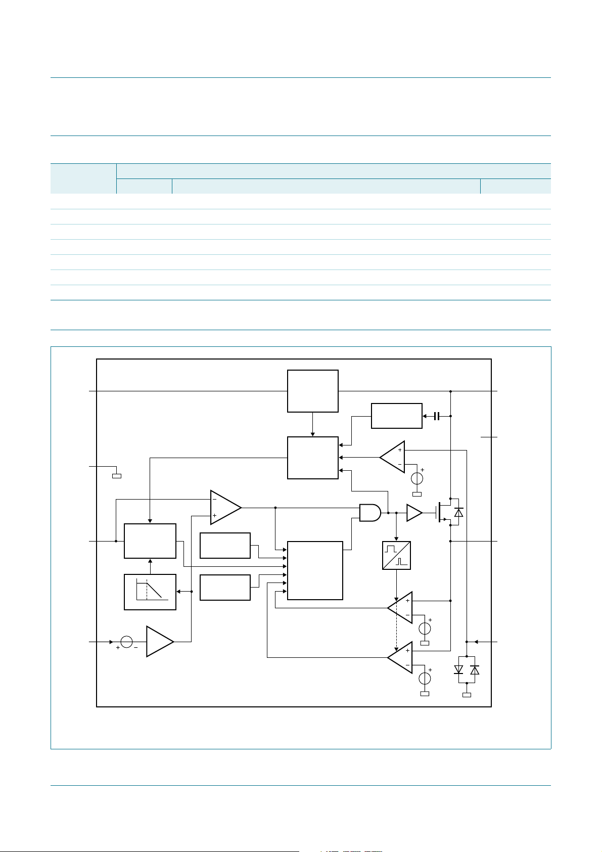
6. Block diagram
V
CC
GND
1 (1)
2 (2, 3, 4,
5, 9, 10)
SUPPLY
VALLEY
TEA152x
LOGIC
100 mV
8 (14)
7 (12, 13)
DRAIN
n.c.
PWM
THERMAL
SHUTDOWN
POWER-UP
RESET
PROTECTION
LOGIC
overcurrent
short circuit winding
blank
0.5 V
0.75 V
6 (11)
5 (8)
SOURCE
AUX
mgt419
RC
REG
3 (6)
4 (7)
stop
OSCILLATOR
low freq
F
1.8 U
2.5 V
10x
Pin numbers without parenthesis refer to DIP8 packages and within parenthesis refer to SO14 packages.
Fig 1. Block diagram
TEA152X All information provided in this document is subject to legal disclaimers. © NXP B.V. 2010. All rights reserved.
Product data sheet Rev. 04 — 14 September 2010 3 of 20
NXP Semiconductors
7. Pinning information
7.1 Pinning
TEA152x
SMPS ICs for low-power systems
14
13
12
11
10
V
CC
GND
RC
REG
1
2
TEA152xP
3
4
001aae137
8
7
6
5
DRAIN
n.c.
SOURCE
AUX
1
V
CC
2
GND n.c.
3
GND n.c.
4
GND SOURCE
GND GND
RC GND
REG AUX
TEA152xT
5
6
7 8
001aae138
Fig 2. Pin configuration DIP8 Fig 3. Pin configuration SO14
7.2 Pin description
Table 3. Pin description
Symbol Pin Description
DIP8 SO14
V
CC
GND 2 2, 3, 4,
RC 36frequency setting
REG 4 7 regul ation input
AUX 5 8 input for voltage from the auxiliary winding for timing
SOURCE 6 11 source of the internal MOS switch
n.c. 7 12, 13 not connected
DRAIN 8 14 drain of the internal MOS switch; input for the start-up current
1 1 supply voltage
ground
5, 9, 10
(demagnetization)
and valley sensing
DRAIN
9
8. Functional description
The TEA152x family is the heart of a compact flyback converter, with the IC placed at the
primary side. The auxiliary winding of the transformer can be used for indirect feedback to
control the isolated output. This additional winding also powers the IC. A more accurate
control of the output voltage and/or current can be implemented with an additional
secondary sensing circuit and optocoupler feedback.
The TEA152x family uses voltage mode control. The frequency is determined by the
maximum transformer demagnetizing time and the time of the oscillator. In the first case,
the converter operates in the Self-Oscillating Power Supply (SOPS) mode. In the latter
case, it operates at a constant frequency, which can be adjusted with external
TEA152X All information provided in this document is subject to legal disclaimers. © NXP B.V. 2010. All rights reserved.
Product data sheet Rev. 04 — 14 September 2010 4 of 20

NXP Semiconductors
components RRC and CRC. This mode is called Pulse Width Modulation (PWM).
Furthermore, a primary stroke is started only in a valley of the secondary ringing. This
valley switching principle minimizes capacitive switch-on losses.
8.1 Start-up and Underoltage lockout
Initially , the IC is self supplying from the rectified main s volt age. The IC st art s switching as
soon as the voltage on pin VCC passes the V
the auxiliary winding of the transformer as soon as V
from the line is stopped for high efficiency operation.
When for some reason the auxiliary supply is not sufficient, the high-voltage supply also
supplies the IC. As soon as the voltage on pin V
stops switching and restarts from the rectified mains voltage.
8.2 Oscillator
The frequency of the oscillator is set by the external resistor and capacitor on pin RC. The
external capacitor is charged rapidly to the V
stroke, it discharges to the V
relative sensitivity of the duty factor to the regulation voltage at low duty factor is almost
equal to the sensitivity at high duty factors. This results in a more constant gain over the
duty factor range compared to PWM systems with a linear sawtooth oscillator. Stable
operation at low duty factors is easily realized. For high efficiency, the frequency is
reduced as soon as the duty factor drops below a certain value. This is accomplished by
increasing the oscillator charge time.
SMPS ICs for low-power systems
CC(startup)
RC(max)
level. Because the discharge is exponential, the
RC(min)
level. The supply is taken over by
is high enough and the supply
CC
drops below the V
CC
CC(stop)
level and, starting from a new primar y
TEA152x
level, the IC
To ensure that the capacitor can be charged within the cha rge time, the value of the
oscillator capacitor should be limited to approximately 1 nF.
8.3 Duty factor control
The duty factor is controlled by the internal regulation voltage and the oscillator signal on
pin RC. The internal regulation volt age is eq ual to the extern al reg ulation voltage (−2.5 V)
multiplied by the gain of the error amplifier (typically 20 dB which is 10×).
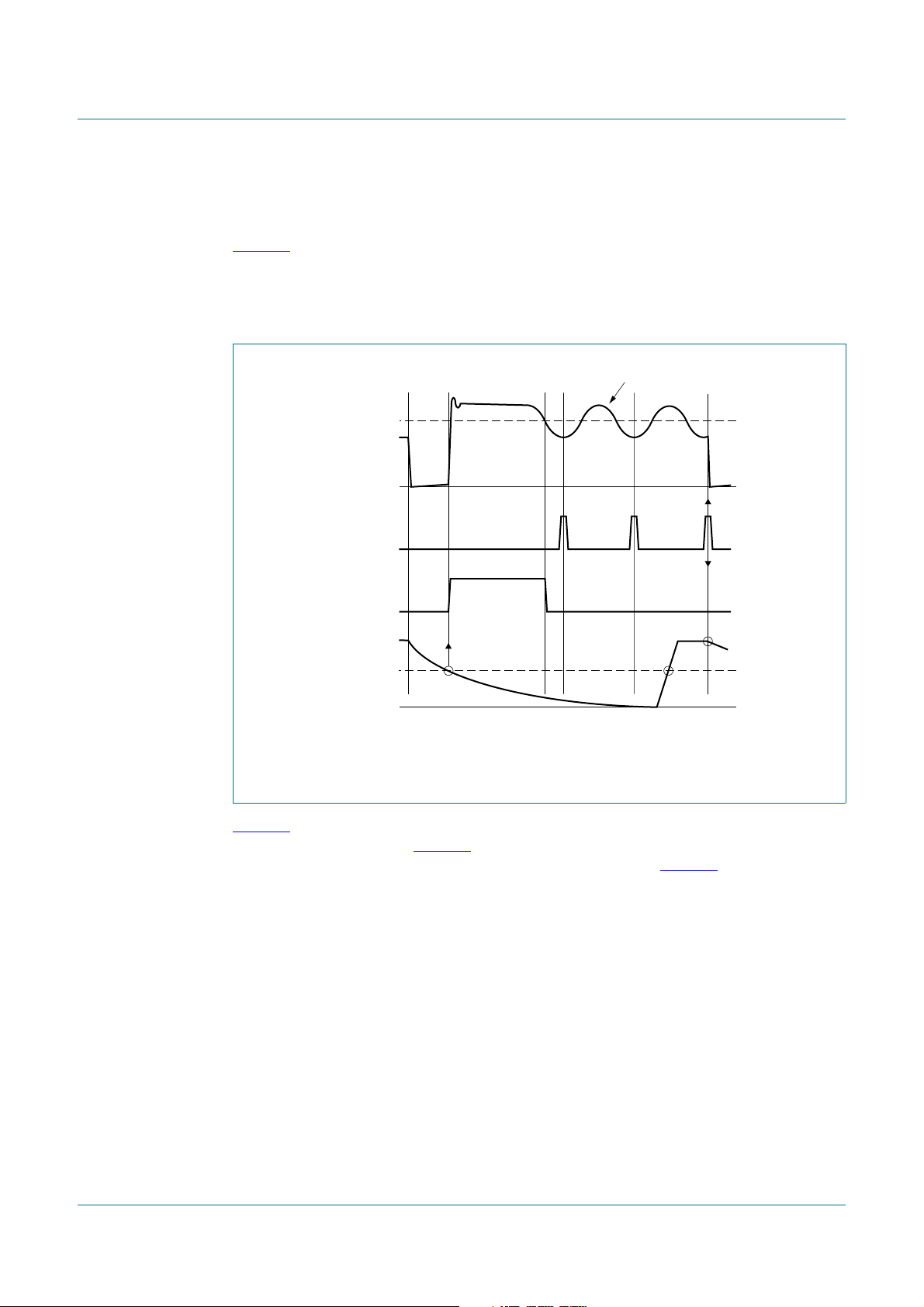
8.4 Valley switching
A new cycle is started when the primary switch is switched on (see Figure 4). After a
certain time (determined by the oscillator voltage RC and the internal regulation level), the
switch is turned off and the secondary stroke starts. The internal regulation level is
determined by the voltage on pin REG.
After the secondary stroke, the drain voltage shows an oscillation with a frequency of
approximately:
----------------------------------------------
2 π× LpC
where:
1
×()×
p
L
= primary self-inductance
p
C
= parasitic capacitance on drain node
p
(1)
TEA152X All information provided in this document is subject to legal disclaimers. © NXP B.V. 2010. All rights reserved.
Product data sheet Rev. 04 — 14 September 2010 5 of 20
NXP Semiconductors
3
As soon as the oscillator voltage is high again and the secondary stroke has ended, the
circuit waits for a low drain voltage before starting a new primary stroke.
TEA152x
SMPS ICs for low-power systems
Figure 4
shows the drain voltage together with the valley signal, the signal indicating the
secondary stroke and the RC voltage.
The primary stroke starts some time before the actu al valley at low ringing frequencies,
and some time after the actual valley at high ringing frequencies.
secondary
ringing
B
A
drain
valley
secondary
stroke
RC
oscillator
primary
stroke
secondary
stroke
regulation level
mgt42
A: Start of new cycle with valley switching
B: Start of new cycle in a classical PWM system
Fig 4. Signals for valley switching
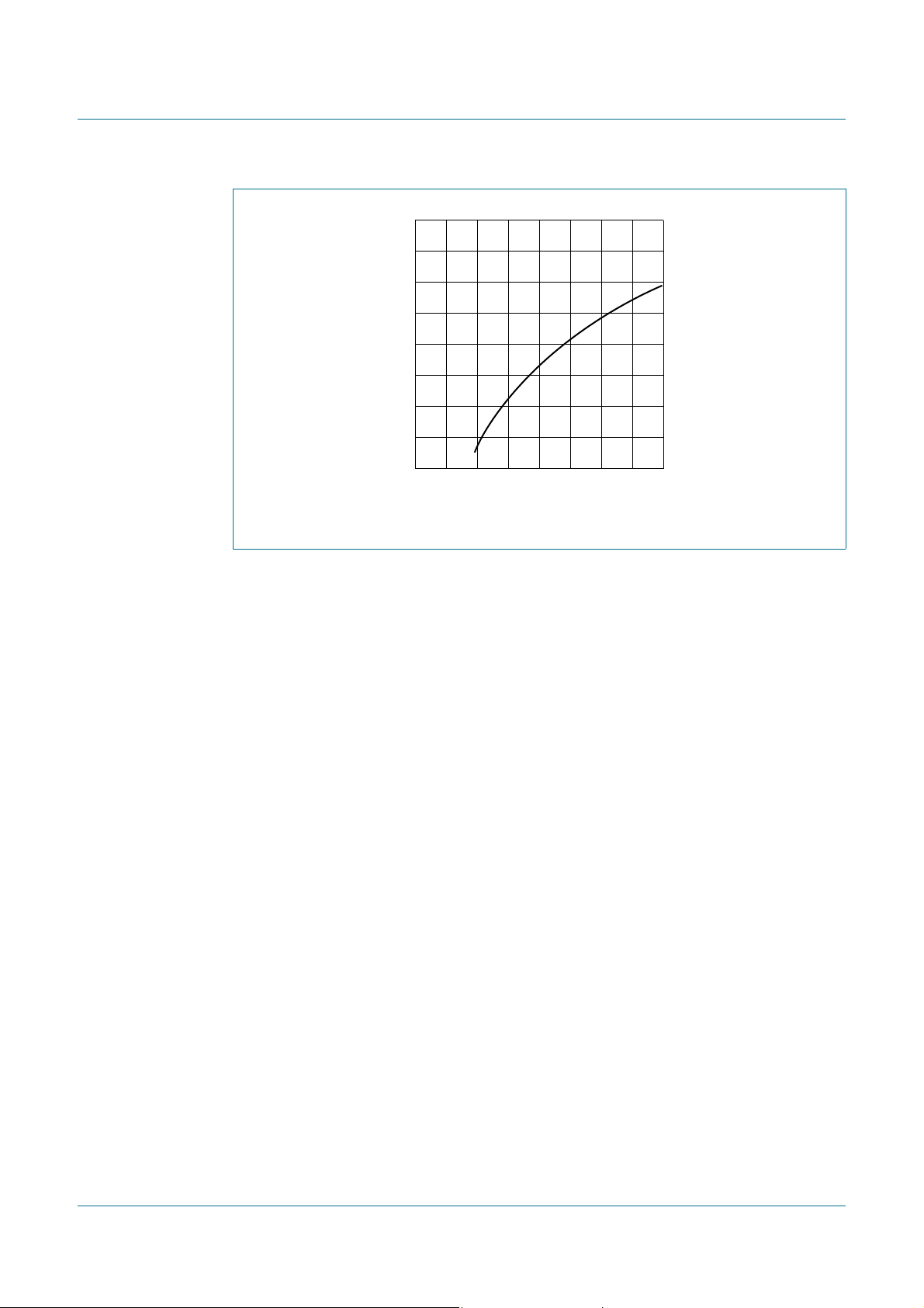
Figure 5 shows a typical curve for a reflected output voltage N × Vo of 80 V. This voltage is
the output voltage Vo (see
the factor N (determined by the turns ratio of the transformer).
Figure 6) transferred to the primary side of the transformer with
Figure 5 shows that the
system switches exactly at minimum drain voltage for ringing frequencies of 480 kHz, thus
reducing the switch-on losses to a minimum. At 200 kHz, the next primary stroke is started
at 33° before the valley. The switch-on losses are still reduced significantly.
TEA152X All information provided in this document is subject to legal disclaimers. © NXP B.V. 2010. All rights reserved.
Product data sheet Rev. 04 — 14 September 2010 6 of 20
NXP Semiconductors
mgt424
Fig 5. Typical phase of drain ringing at switch-on (at N × Vo=80V)
40
phase
(deg)
20
0
−20
−40
0 200 400 800
TEA152x
SMPS ICs for low-power systems
600
f (kHz)
8.5 Demagnetization
The system operates in discontinuous conduction mode all the time. As long as the
secondary stroke has not ended, the oscillator will not start a new primary stroke. During
the first t
seconds, demagnetization recognition is suppressed. This suppressio n may
suppr
be necessary in applications where the transformer has a large leakage induct ance and at
low output voltages.
8.6 Minimum and maximum duty factor
The minimum duty factor of the switched mode power supply is 0 %. The maximum duty
factor is set to 75 % (typical value at 100 kHz oscillation frequency).
8.7 OverCurrent Protection (OCP)
The cycle-by-cycle peak drain current limit circuit uses the external source resistor RI to
measure the current. The circuit is activated after the leading edge bla nking time t
protection circuit limits the source voltage to V
source(max)
, and thus limits the primary peak
current.
8.8 Short-circuit winding protection
The short-circuit winding protection circuit is also activated af ter the leading edge bla nking
time. If the source voltage exceeds the short-circuit winding protection voltage V
stops switching. Only a power-on reset will restart normal operation. The short-circuit
winding protection also protects in case of a secondary diode short circuit.
leb
swp
. The
, the IC
8.9 OverTemperature Protection (OTP)
An accurate temperature protection is provided in the device. When the junction
temperature exceeds the thermal shutdown temperature, the IC stops switching. During
thermal protection, the IC current is lowered to the start-up current. The IC continues
normal operation as soon as the overtemperature situation has disapp eared.
TEA152X All information provided in this document is subject to legal disclaimers. © NXP B.V. 2010. All rights reserved.
Product data sheet Rev. 04 — 14 September 2010 7 of 20

NXP Semiconductors
8.10 OverVoltage Protection (OVP)
Overvoltage protection can be achieved in the application by pulling pin REG above its
normal operation level. The current primary stroke is terminated immediately, and no new
primary stroke is started until the voltage on pin REG drops to its normal operation level.
Pin REG has an internal clamp. The current feed into this pin must be limited.
8.1 1 Output characteristics of complete power-plug
Typical characteristics:
• Output power: A wide range of output power levels can be handled by choosing the
• Accuracy: The accuracy of the complete conv er te r, functioning as a voltage source
• Efficiency: An efficiency of 75 % at maximum output power can be achieved for a
• Ripple: A minimum ripple is obtained in a system designed for a maximum duty factor
TEA152x
SMPS ICs for low-power systems
R
with primary sensing, is approximately 8 % (mainly dependent on the transformer
coupling). The accuracy with secondary sensing is defined by the accuracy of the
external components. For safety requirements in case of optocoupler feedback loss,
the primary sensing remains active when an over vo ltage circuit is conn ec te d.
complete converter designed for universal mains.
of 50 % under normal operating conditions, and a minimized dead time. The
magnitude of the ripple in the output voltage is determined by the frequency and duty
factor of the converter, the output cur rent level and the value and ESR of the output
capacitor.
and package of the TEA152x family. Power levels up to 30 W can be realized.
DS(on)
8.12 Input characteristics of complete power-plug
Typical characteristics:
• The input voltage range comprises the universal AC mains (80 V to 276 V)
TEA152X All information provided in this document is subject to legal disclaimers. © NXP B.V. 2010. All rights reserved.
Product data sheet Rev. 04 — 14 September 2010 8 of 20

NXP Semiconductors
9. Limiting values
Table 4. Limiting values
In accordance with the Absolute Maximum Rating System (IEC 60134). All voltages are measured
with respect to ground; positive currents flow into the device; pins V
current driven and pins REG and AUX are not allowed to be voltage driven.
Symbol Parameter Conditions Min Max Unit
Voltages
V
CC
V
RC
V
source
V
drain
Currents
I
REG
I
AUX
I
source
I
drain
General
P
tot
T
stg
T
j
V
esd
TEA152x
SMPS ICs for low-power systems
and RC are not allowed to be
CC
supply voltage continuous −0.4 +40 V
voltage on pin RC −0.4 +3 V
voltage on pin SOURCE DMOS power
transistor
voltage on pin DRAIN Tj>0°C −0.4 +650 V
current on pin REG - 6 mA
current on pin AUX −10 +5 mA
source current
TEA1520x −0.25 +0.25 A
TEA1521x −0.5 +0.5 A
TEA1522x −1+1A
TEA1523P −2+2A
drain current
TEA1520x −0.25 +0.25 A
TEA1521x −0.5 +0.5 A
TEA1522x −1+1A
TEA1523P −2+2A
total power dissipation
DIP8 package T
SO14 package T
<45°C-1.0W
amb
<50°C-1.0W
amb
storage temperature −55 +150 °C
junction temperature −40 +145 °C
electrostatic discharge voltage human body model
machine model
−0.4 +5 V
[1]
- ±2500 V
[2]
- ±200 V
[1] Human body model: equivalent to discharging a 100 pF capacitor through a 1.5 kΩ series resistor. All pins
are 2500 V maximum, except pin DRAIN, which is 1000 V maximum.
[2] Machine model: equivalent to discharging a 200 pF capacitor through a 0.75 μH coil and a 10 Ω series
resistor.
TEA152X All information provided in this document is subject to legal disclaimers. © NXP B.V. 2010. All rights reserved.
Product data sheet Rev. 04 — 14 September 2010 9 of 20

NXP Semiconductors
10. Thermal characteristics
Table 5. Thermal characteristics
Symbol Parameter Conditions Typ Unit
R
th(j-a)
thermal resistance from junction to ambient in free air
DIP8 package 100 K/W
SO14 package 91 K/W
TEA152x
SMPS ICs for low-power systems
[1]
[1] Thermal resistance R
printed-circuit board. See the TEA152x application note for details.
11. Characteristics
Table 6. Characteristics
T
amb
positive when flowing into the IC; unless otherwise specified.
Symbol Parameter Conditions Min Typ Max Unit
Supply
I
CC(oper)
I
CC(startup)
I
CC(ch)
V
CC(startup)
V
CC(stop)
I
drain
Pulse-width modulator
δ
min
δ
max
SOPS
V
det(demag)
t
sup(xfmr_ring)
RC oscillator
V
RC(min)
V
RC(max)
t
ch(RC)
f
osc
Duty factor regulator: pin REG
V
REG
G
v
V
clamp(REG)
can be lower when the GND pins are connected to sufficient copper area on the
th(j-a)
=25°C; no overtemperature; all voltages are measured with respect to ground; currents are
operating supply current normal operation - 1.3 1.9 mA
start-up supply current start-up - 180 400 μA
charge supply current V
>60V −6 −4 −3mA
drain
start-up supply voltage 9 9.5 10 V
stop supply voltage undervoltage lockout 7.0 7.5 8.0 V
current on pin DRAIN V
drain
>60V
no auxiliary supply - 1.5 2 mA
with auxiliary
- 30 125 μA
supply
minimum duty factor - 0 - %
maximum duty cycle f = 100 kHz - 75 - %
demagnetization detection
50 100 150 mV
voltage
transformer ringing
start of 2nd stroke 1.0 1.5 2.0 μs
suppression time
minimum voltage on pin RC 60 75 90 mV
maximum voltage on pin RC 2.4 2.5 2.6 V
charge time on pin RC - 1 - μs
oscillator frequency 10 100 200 kHz
voltage on pin REG 2.4 2.5 2.6 V
voltage gain error amplifier - 20 - dB
clamp voltage on pin REG I
=6mA --7.5V
REG
TEA152X All information provided in this document is subject to legal disclaimers. © NXP B.V. 2010. All rights reserved.
Product data sheet Rev. 04 — 14 September 2010 10 of 20

NXP Semiconductors
Table 6. Characteristics …continued
T
amb
positive when flowing into the IC; unless otherwise specified.
Symbol Parameter Conditions Min Typ Max Unit
Valley switching
(ΔV/Δt)
f
valley
t
d(vrec-swon)
Current and short-circuit winding protection
V
source(max)
t
d(prop)
V
swp
t
leb
FET output stage
I
L(drain)
V
BR(DRAIN)
R
DSon
t
f(DRAIN)
Temperature protection
T
prot(max)
T
prot(hys)
TEA152x
SMPS ICs for low-power systems
=25°C; no overtemperature; all voltages are measured with respect to ground; currents are
vrec
valley recognition voltage
change with time
ringing frequency for valley
N × Vo= 100 V 200 550 800 kHz
switching
valley recognition to
switch-on delay time
maximum voltage on pin
ΔV/Δt=0.1V/μs 0.470.500.53V
SOURCE
delay from detecting
V
source(max)
to switch-off
short-winding protection
ΔV/Δt=0.5V/μs - 160 185 ns
ΔV/Δt=0.5V/μs 0.7 0.75 0.8 V
voltage
leading edge blanking time 250 350 450 ns
leakage current on pin
V
= 650 V - - 125 μA
drain
DRAIN
breakdown voltage on pin
Tj>0°C 650 - - V
DRAIN
drain-source on-state
resistance
TEA1520x I
TEA1521x I
TEA1522x I
TEA1523P I
= −0.06 A
source
=25°C - 48 55.2 Ω
T
j
=100°C - 68 78.2 Ω
T
j
= −0.125 A
source
=25°C - 24 27.6 Ω
T
j
=100°C - 34 39.1 Ω
T
j
= −0.25 A
source
=25°C - 12 13.8 Ω
T
j
=100°C - 17 19.6 Ω
T
j
= −0.50 A
source
=25°C-6.57.5Ω
T
j
=100°C - 9.0 10.0 Ω
T
j
fall time on pin DRAIN Vi=300V;
no external capacitor
at drain
maximum threshold
temperature
hysteresis of protection
temperature
−102 - +102 V/μs
-150-ns
-75-ns
150 160 170 °C
-2-°C
TEA152X All information provided in this document is subject to legal disclaimers. © NXP B.V. 2010. All rights reserved.
Product data sheet Rev. 04 — 14 September 2010 11 of 20

NXP Semiconductors
12. Application information
TEA152x
SMPS ICs for low-power systems
LF
C
VCC
R
C
CF2
RC
RC
V
CC
GND
RC
REG
R2
1
2
TEA152xP
3
4
D2
8
7
6
5
DRAIN
n.c.
SOURCE
AUX
CF1
mains
R1
R4
R3
Fig 6. Primary sensed application; configuration for TEA152xP (DIP8)
Further application information can be found in the TEA152x application note.
D5
mgt425
V
o
Z1
D1
R
I
R
AUX
C5
C6 - Ycap
TEA152X All information provided in this document is subject to legal disclaimers. © NXP B.V. 2010. All rights reserved.
Product data sheet Rev. 04 — 14 September 2010 12 of 20

NXP Semiconductors
D
-1
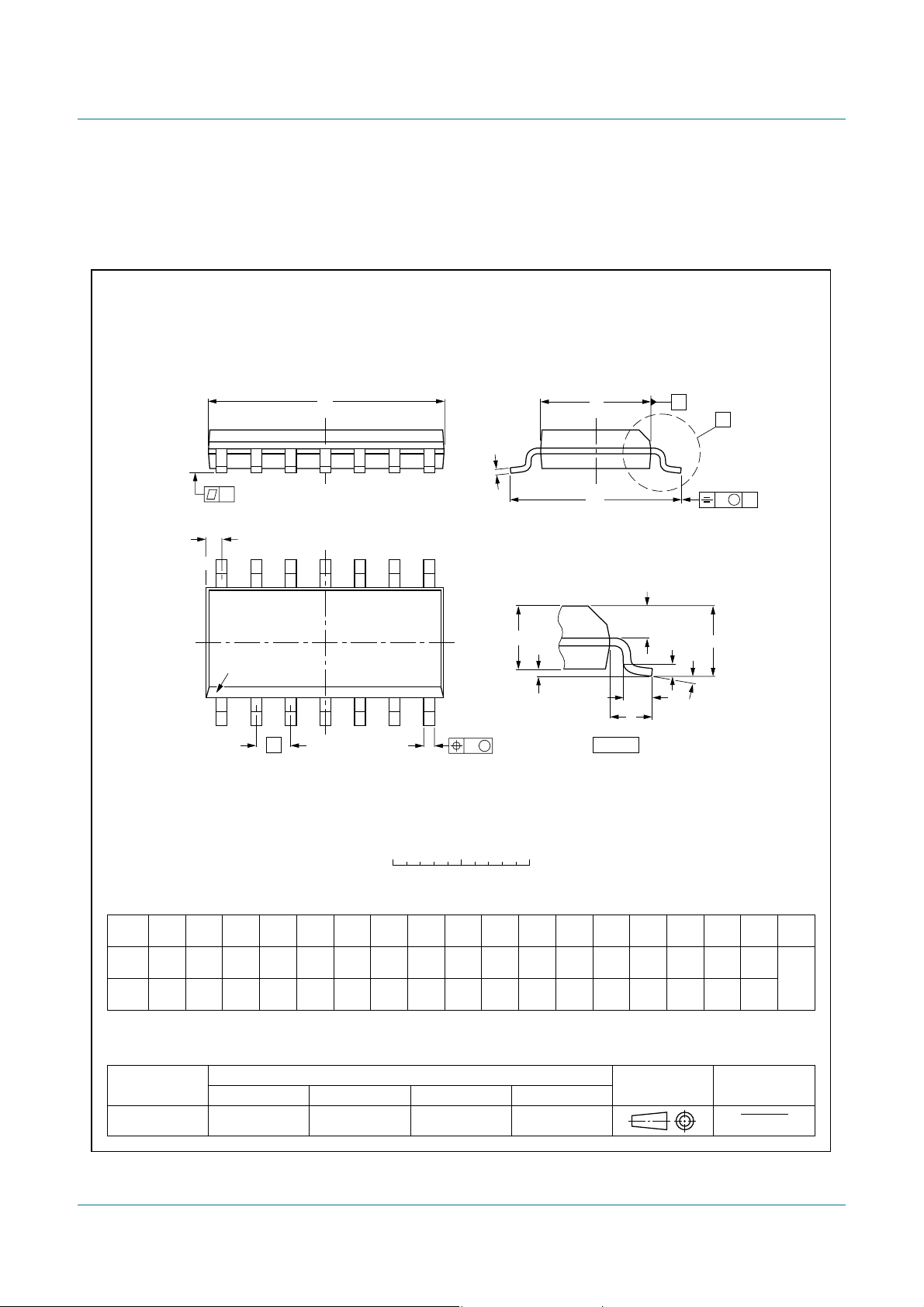
13. Package outline
TEA152x
SMPS ICs for low-power systems
IP8: plastic dual in-line package; 8 leads (300 mil)
D
M
E
A
2
1
2
w M
A
c
(e )
1
M
H
E
seating plane
L
Z
8
pin 1 index
A
b
e
b
1
b
5
SOT97
1
DIMENSIONS (inch dimensions are derived from the original mm dimensions)
A
A
12
min.
max.
050G01 MO-001 SC-504-8
b
1.73
1.14
0.068
0.021
0.045
0.015
IEC JEDEC JEITA
mm
OUTLINE
VERSION
SOT97-1
A
max.
UNIT
inches
Note
1. Plastic or metal protrusions of 0.25 mm (0.01 inch) maximum per side are not included.
b
0.53
0.38
1
4
0 5 10 mm
scale
b
2
1.07
0.36
0.89
0.23
0.014
0.042
0.009
0.035
REFERENCES
(1) (1)
cD E e M
9.8
6.48
9.2
6.20
0.39
0.26
0.36
0.24
1
3.60
3.05
0.14
0.12
E
8.25
7.80
0.32
0.31
EUROPEAN
PROJECTION
10.0
0.39
0.33
M
L
e
H
8.3
w
max.
0.2542.54 7.62
1.154.2 0.51 3.2
0.010.1 0.3
0.0450.17 0.02 0.13
ISSUE DATE
99-12-27
03-02-13
(1)
Z
Fig 7. Package outline SOT97-1 (DIP8)
TEA152X All information provided in this document is subject to legal disclaimers. © NXP B.V. 2010. All rights reserved.
Product data sheet Rev. 04 — 14 September 2010 13 of 20
NXP Semiconductors
S
-1
TEA152x
SMPS ICs for low-power systems
O14: plastic small outline package; 14 leads; body width 3.9 mm
y
Z
14
pin 1 index
1
e
D
c
8
A
2
A
1
7
w M
b
p
E
H
E
detail X
A
X
v M
Q
(A )
L
p
L
A
3
θ
SOT108
A
0 2.5 5 mm
scale
DIMENSIONS (inch dimensions are derived from the original mm dimensions)
A
UNIT
mm
inches
Note
1. Plastic or metal protrusions of 0.15 mm (0.006 inch) maximum per side are not included.
OUTLINE
VERSION
SOT108-1
A1A2A3b
max.
0.25
1.75
0.10
0.010
0.069
0.004
p
1.45
1.25
0.057
0.049
IEC JEDEC JEITA
076E06 MS-012
0.25
0.01
0.49
0.36
0.019
0.014
0.25
0.19
0.0100
0.0075
(1)E(1)
cD
8.75
8.55
0.35
0.34
REFERENCES
eHELLpQZywv θ
1.27
0.05
6.2
5.8
0.244
0.228
4.0
3.8
0.16
0.15
1.05
0.041
1.0
0.4
0.039
0.016
0.7
0.25
0.6
0.028
0.01 0.004
0.024
EUROPEAN
PROJECTION
0.25 0.1
0.01
(1)
0.7
0.3
0.028
0.012
ISSUE DATE
99-12-27
03-02-19
o
8
o
0
Fig 8. Package outline SOT108-1 (SO14)
TEA152X All information provided in this document is subject to legal disclaimers. © NXP B.V. 2010. All rights reserved.
Product data sheet Rev. 04 — 14 September 2010 14 of 20

NXP Semiconductors
TEA152x
SMPS ICs for low-power systems
14. Abbreviations
Table 7. Abbreviations
Acronym Description
BiCMOS Bipolar Complementary Metal-Oxide Semiconductor
DMOS Diffusion Metal-Oxide Semiconductor
ESR Equivalent Series Resistance
EZ-HV SOI Easy High Voltage Silicon-On-Insulator
FET Field-Effect Transistor
PWM Pulse Width Modulation
SMPS Switched Mode Power Supply
SOPS Self-Oscillating Power Supply
15. Revision history
Table 8. Revision history
Document ID Release date Data sheet status Change notice Supersedes
TEA152X v4.0 20100914 Product data sheet - TEA152X_3
Modifications:
TEA152X_3 20090323 Product data sheet - TEA152X_FAM_2
Modifications: • The format of this data sheet has been redesigned to comply with the new identity
TEA152X_FAM_2 20060125 Product data sheet - TEA152X_FAMILY_1
TEA152X_FAMILY_1 20000908 Product specification - -
•
Table 1 “Quick reference data” updated
Table 4 “Limiting values” updated
•
guidelines of NXP Semiconductors.
• Legal texts have been adapted to the new company name where appropriate.
• The minimum value of T
• The minimum value of T
has changed in Table 1 and Table 4
amb
has changed in Table 4
j
TEA152X All information provided in this document is subject to legal disclaimers. © NXP B.V. 2010. All rights reserved.
Product data sheet Rev. 04 — 14 September 2010 15 of 20

NXP Semiconductors
TEA152x
SMPS ICs for low-power systems
16. Legal information
16.1 Data sheet status
Document status
Objective [short] data sheet Development This document contains data from the objective specification for product development.
Preliminary [short] data sheet Qualification This document contains data from the preliminary specification.
Product [short] data sheet Production This document contains the product specification.
[1] Please consult the most recently issued document before initiating or completing a design.
[2] The term ‘short data sheet’ is explained in section “Definitions”.
[3] The product status of device(s) d escribed i n this docume nt may have changed since this docume nt was publis hed and ma y dif fer in case of multiple devices. The latest product status
information is available on the Internet at URL
[1][2]
Product status
http://www.nxp.com.
[3]
Definition
16.2 Definitions
Draft — The document is a draft version only. The content is still under
internal review and subject to formal approval, which may result in
modifications or additions. NXP Semiconductors does not give any
representations or warranties as to the accuracy or completeness of
information included herein and shall have no liability for the consequences of
use of such information.
Short data sheet — A short data sheet is an extract from a full data sheet
with the same product type number(s) and title. A short data sheet is intended
for quick reference only and should not be relied u pon to co nt ain det ailed and
full information. For detailed and full information see the relevant full data
sheet, which is available on request via the local NXP Semiconductors sales
office. In case of any inconsistency or conflict with the short data sheet, the
full data sheet shall prevail.
Product specification — The information and data provided in a Product
data sheet shall define the specification of the product as agreed between
NXP Semiconductors and its customer, unless NXP Semiconductors and
customer have explicitly agreed otherwise in writing. In no event however,
shall an agreement be valid in which the NXP Semiconductors product is
deemed to offer functions and qualities beyond those described in the
Product data sheet.
16.3 Disclaimers
Limited warranty and liability — Information in this document is believed to
be accurate and reliable. However, NXP Semiconductors does not give any
representations or warranties, expressed or implied, as to the accuracy or
completeness of such information and shall have no liability for the
consequences of use of such information.
In no event shall NXP Semiconductors be lia ble for any indirect, incidental,
punitive, special or consequential damages (including - without limitation - lost
profits, lost savings, business interruption, costs related to the removal or
replacement of any products or rework charges) whether or not such
damages are based on tort (including negligence), warranty, breach of
contract or any other legal theory.
Notwithstanding any damages that customer might incur for any reason
whatsoever, NXP Semi conductors’ aggregat e and cumulative liabil ity towards
customer for the products described herein shall be limited in accordance
with the Terms and conditions of commercial sale of NXP Semiconductors.
Right to make changes — NXP Semiconductors reserves the right to make
changes to information published in this document, including without
limitation specifications and product descriptions, at any time and without
notice. This document supersedes and replaces all information supplied prior
to the publication hereof.
Suitability for use — NXP Semiconductors products are not designed,
authorized or warranted to be suitable for use in life support, life-critical or
safety-critical systems or equipment, nor in applications where failure or
malfunction of an NXP Semiconductors product can reasonabl y be expected
to result in personal injury, death or severe property or environmental
damage. NXP Semiconductors accepts no liability for inclusion and/or use of
NXP Semiconductors products in such equipment or applications and
therefore such inclusion and/or use is at the customer’s own risk.
Applications — Applications that are described herein for any of these
products are for illustrative purposes only. NXP Semiconductors makes no
representation or warranty that such applications will be suitable for the
specified use without further testing or modification.
Customers are responsible for the design and operation of their applications
and products using NXP Semiconductors products, and NXP Semiconductors
accepts no liability for any assistance with applications or customer product
design. It is customer’s sole responsibility to determine whether the NXP
Semiconductors product is suitable and fit for the customer’s applications and
products planned, as well as for the planned application and use of
customer’s third party customer(s). Customers should provide appropriate
design and operating safeguards to minimize the risks associated with their
applications and products.
NXP Semiconductors does not accept any liability related to any default ,
damage, costs or problem which is based on any weakness or default in the
customer’s applications or products, or the application or use by customer’s
third party customer(s). Customer is responsible for doing all necessary
testing for the customer’s applications and products using NXP
Semiconductors products in order to avoid a default of the applications and
the products or of the application or use by customer’s third part y
customer(s). NXP does not accept any liability in this respect.
Limiting values — Stress above one or more limiting values (as defined in
the Absolute Maximum Ratings System of IEC 60134) will cause permanent
damage to the device. Limiting values are stress ratings only and (proper)
operation of the device at these or any other conditions above those given in
the Recommended operating conditions section (if present) or the
Characteristics sections of this document is not warranted. Constant or
repeated exposure to limiting values will permanently and irreversibly affect
the quality and reliability of the device.
Terms and conditions of commercial sale — NXP Semiconductors
products are sold subject to the general terms and conditions of commercial
sale, as published at
agreed in a valid written individual agreement. In case an individual
agreement is concluded only the terms and conditions of the respective
agreement shall apply. NXP Semiconductors hereby expressly objects to
applying the customer’s general terms and conditions with regard to the
purchase of NXP Semiconductors products by customer.
No offer to sell or license — Nothing in this document may be interpreted or
construed as an offer to sell product s that is ope n for accept ance or the gr ant,
conveyance or implication of any license under any copyrights, patents or
other industrial or intellectual property rights.
Export control — This document as well as the item(s) described herein
may be subject to export control regulations. Export might require a prior
authorization from national authorities.
http://www.nxp.com/profile/terms
, unless otherwise
TEA152X All information provided in this document is subject to legal disclaimers. © NXP B.V. 2010. All rights reserved.
Product data sheet Rev. 04 — 14 September 2010 16 of 20

NXP Semiconductors
TEA152x
SMPS ICs for low-power systems
Quick reference data — The Quick reference data is an extract of the
product data given in the Limiting values and Characteristics sections of this
document, and as such is not complete, exhaustive or legally binding.
Non-automotive qualified products — Unless this data sheet expressly
states that this specific NXP Semiconductors product is automotive qualified,
the product is not suitable for automotive use. It i s neither qua lif ied nor test ed
in accordance with automotive testing or application requirements. NXP
Semiconductors accepts no liability for inclusion and/or use of
non-automotive qualified products in automotive equ ipment or applications.
In the event that customer uses the product for design-in and use in
automotive applications to automotive specifications and standards, customer
(a) shall use the product without NXP Semiconductors’ warranty of the
product for such automotive applications, use and specifications, and (b)
whenever customer uses the product for automotive applications beyond
NXP Semiconductors’ specifications such use shall be solely at customer’s
own risk, and (c) customer fully indemnifies NXP Semiconductors for any
liability, da mages or failed produ ct cl aims resulting from custome r design and
use of the product for automotive applications beyond NXP Semiconductors’
standard warranty and NXP Semiconductors’ product specifications.
16.4 Trademarks
Notice: All referenced brands, prod uct names, service names and trad emarks
are the property of their respective owners.
STARplug — is a trademark of NXP B.V.
EZ-HV — is a trademark of NXP B.V.
17. Contact information
For more information, please visit: http://www.nxp.com
For sales office addresses, please send an email to: salesaddresses@nxp.com
TEA152X All information provided in this document is subject to legal disclaimers. © NXP B.V. 2010. All rights reserved.
Product data sheet Rev. 04 — 14 September 2010 17 of 20

NXP Semiconductors
18. Tables
Table 1. Quick reference data . . . . . . . . . . . . . . . . . . . . .2
Table 2. Ordering information . . . . . . . . . . . . . . . . . . . . .3
Table 3. Pin description . . . . . . . . . . . . . . . . . . . . . . . . . .4
Table 4. Limiting values . . . . . . . . . . . . . . . . . . . . . . . . . .9
Table 5. Thermal characteristics . . . . . . . . . . . . . . . . . .10
Table 6. Characteristics . . . . . . . . . . . . . . . . . . . . . . . . .10
Table 7. Abbreviations . . . . . . . . . . . . . . . . . . . . . . . . . .15
Table 8. Revision history . . . . . . . . . . . . . . . . . . . . . . . .15
TEA152x
SMPS ICs for low-power systems
continued >>
TEA152X All information provided in this document is subject to legal disclaimers. © NXP B.V. 2010. All rights reserved.
Product data sheet Rev. 04 — 14 September 2010 18 of 20

NXP Semiconductors
19. Figures
Fig 1. Block diagram . . . . . . . . . . . . . . . . . . . . . . . . . . . .3
Fig 2. Pin configuration DIP8. . . . . . . . . . . . . . . . . . . . . .4
Fig 3. Pin configuration SO14 . . . . . . . . . . . . . . . . . . . . .4
Fig 4. Signals for valley switching . . . . . . . . . . . . . . . . . .6
Fig 5. Typical phase of drain ringing at switch-on
(at N × Vo= 80 V). . . . . . . . . . . . . . . . . . . . . . . . . .7
Fig 6. Primary sensed application; configuration
for TEA152xP (DIP8). . . . . . . . . . . . . . . . . . . . . .12
Fig 7. Package outline SOT97-1 (DIP8) . . . . . . . . . . . .13
Fig 8. Package outline SOT108-1 (SO14) . . . . . . . . . . .14
TEA152x
SMPS ICs for low-power systems
continued >>
TEA152X All information provided in this document is subject to legal disclaimers. © NXP B.V. 2010. All rights reserved.
Product data sheet Rev. 04 — 14 September 2010 19 of 20

NXP Semiconductors
20. Contents
1 General description. . . . . . . . . . . . . . . . . . . . . . 1
2 Features and benefits . . . . . . . . . . . . . . . . . . . . 1
3 Applications . . . . . . . . . . . . . . . . . . . . . . . . . . . . 2
4 Quick reference data . . . . . . . . . . . . . . . . . . . . . 2
5 Ordering information. . . . . . . . . . . . . . . . . . . . . 3
6 Block diagram . . . . . . . . . . . . . . . . . . . . . . . . . . 3
7 Pinning information. . . . . . . . . . . . . . . . . . . . . . 4
7.1 Pinning . . . . . . . . . . . . . . . . . . . . . . . . . . . . . . . 4
7.2 Pin description . . . . . . . . . . . . . . . . . . . . . . . . . 4
8 Functional description . . . . . . . . . . . . . . . . . . . 4
8.1 Start-up and Underoltage lockout . . . . . . . . . . . 5
8.2 Oscillator. . . . . . . . . . . . . . . . . . . . . . . . . . . . . . 5
8.3 Duty factor control . . . . . . . . . . . . . . . . . . . . . . 5
8.4 Valley switching . . . . . . . . . . . . . . . . . . . . . . . . 5
8.5 Demagnetization. . . . . . . . . . . . . . . . . . . . . . . . 7
8.6 Minimum and maximum duty factor . . . . . . . . . 7
8.7 OverCurrent Protection (OCP) . . . . . . . . . . . . . 7
8.8 Short-circuit winding protection. . . . . . . . . . . . . 7
8.9 OverTemperature Protection (OTP) . . . . . . . . . 7
8.10 OverVoltage Protection (OVP) . . . . . . . . . . . . . 8
8.1 1 Output characteristics of complete power-plug. 8
8.12 Input characteristics of complete power-plug . . 8
9 Limiting values. . . . . . . . . . . . . . . . . . . . . . . . . . 9
10 Thermal characteristics . . . . . . . . . . . . . . . . . 10
11 Characteristics. . . . . . . . . . . . . . . . . . . . . . . . . 10
12 Application information. . . . . . . . . . . . . . . . . . 12
13 Package outline . . . . . . . . . . . . . . . . . . . . . . . . 13
14 Abbreviations. . . . . . . . . . . . . . . . . . . . . . . . . . 15
15 Revision history. . . . . . . . . . . . . . . . . . . . . . . . 15
16 Legal information. . . . . . . . . . . . . . . . . . . . . . . 16
16.1 Data sheet status . . . . . . . . . . . . . . . . . . . . . . 16
16.2 Definitions. . . . . . . . . . . . . . . . . . . . . . . . . . . . 16
16.3 Disclaimers. . . . . . . . . . . . . . . . . . . . . . . . . . . 16
16.4 Trademarks. . . . . . . . . . . . . . . . . . . . . . . . . . . 17
17 Contact information. . . . . . . . . . . . . . . . . . . . . 17
18 Tables . . . . . . . . . . . . . . . . . . . . . . . . . . . . . . . . 18
19 Figures . . . . . . . . . . . . . . . . . . . . . . . . . . . . . . . 19
20 Contents . . . . . . . . . . . . . . . . . . . . . . . . . . . . . . 20
TEA152x
SMPS ICs for low-power systems
Please be aware that important notices concerning this document and the product(s)
described herein, have been included in section ‘Legal information’.
© NXP B.V. 2010. All rights reserved.
For more information, please visit: http://www.nxp.com
For sales office addresses, please send an email to: salesaddresses@nxp.com
Date of release: 14 September 2010
Document identifier: TEA152X

 Loading...