


INTEGRATED CIRCUITS
DATA SH EET
TDA8552T; TDA8552TS
2 x 1.4 W BTL audio amplifiers with
digital volume control and
headphone sensing
Product specification
Supersedes data of 1998 Jun 02
File under Integrated Circuits, IC01
2002 Jan 04

Philips Semiconductors Product specification
2 x 1.4 W BTL audio amplifiers with digital
volume control and headphone sensing
FEATURES
• One pin digital volume control (for each channel)
• Volume setting with up/down pulses
• Auto repeat function on volume setting
• Headphone sensing
• Maximum gain set by selection pin
• Low sensitivity for EMC radiation
• Internal feedback resistors
• Flexibility in use
• Few external components
• Low saturation voltage of output stage
• Standby mode controlled by CMOS compatible levels
• Low standby current
• No switch-on/switch-off plops
• High supply voltage ripple rejection
• Protected against electrostatic discharge
• Outputs short-circuitsafe to ground, VDDand across the
load
• Thermally protected.
APPLICATIONS
GENERAL DESCRIPTION
TheTDA8552T isatwo channelaudiopower amplifierthat
provides an output power of 2 × 1.4 W into an 8 Ω load
using a 5 V power supply. The circuit contains two BTL
power amplifiers, two digital volume controls and
standby/mute logic. Volume and balance of the amplifiers
are controlled using two digital input pins which can be
driven by simple push-buttons or by a microcontroller.
Using the selection pin(GAINSEL) the maximum gain can
be set at 20 or 30 dB. The headphone sense input (HPS)
can be used to detect if a headphone is plugged into the
jack connector. If a headphone is plugged into the jack
connector the amplifier switches from the BTL to the SE
mode and the BTL loudspeakers are switched off. This
also results in a reduction of quiescent current
consumption.
The TDA8552T is contained in a 20-pin small outline
package. For the TDA8552TS, which is contained in a
20-pin very small outline package, the maximum output
power is limited by the maximum allowed ambient
temperature. More information can be found in Section
“Thermal design considerations”. The SO20 package has
the four corner leads connected to the die pad so that the
thermal behaviour can be improved by the PCB layout.
TDA8552T; TDA8552TS
• Portable consumer products
• Notebook computers
• Communication equipment.
ORDERING INFORMATION
TYPE
NUMBER
TDA8552T SO20 plastic small outline package; 20 leads; body width 7.5 mm SOT163-1
TDA8552TS SSOP20 plastic shrink small outline package; 20 leads; body width 4.4 mm SOT266-1
NAME DESCRIPTION VERSION
PACKAGE
2002 Jan 04 2
Philips Semiconductors Product specification
2 x 1.4 W BTL audio amplifiers with digital
TDA8552T; TDA8552TS
volume control and headphone sensing
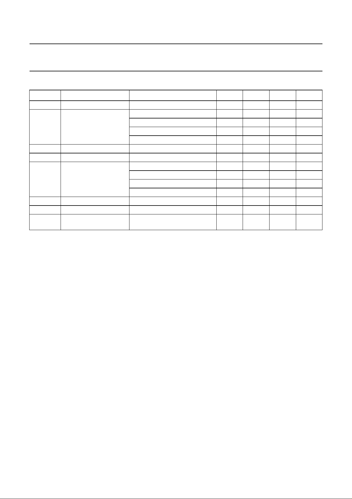
QUICK REFERENCE DATA
SYMBOL PARAMETER CONDITIONS MIN. TYP. MAX. UNIT
V
DD
I
q
I
stb
P
o
G
v
N
step
THD total harmonic distortion P
SVRR supply voltage ripple
supply voltage 2.7 5 5.5 V
quiescent supply current BTL mode; VDD=5V − 14 20 mA
BTL mode; V
SE mode; V
SE mode; V
= 3.3 V − 10 15 mA
DD
=5V − 8.5 12 mA
DD
= 3.3 V − 58mA
DD
standby current − 110µA
output power THD = 10%; RL=8Ω; VDD=5V 1 1.4 − W
voltage gain low gain; maximum volume − 20 − dB
low gain; minimum volume −−60 − dB
high gain; maximum volume − 30 − dB
high gain; minimum volume −−50 − dB
number of volume steps − 64 −
= 0.5 W − 0.1 − %
o
50 −−dB
rejection
2002 Jan 04 3
Philips Semiconductors Product specification
h
2 x 1.4 W BTL audio amplifiers with digital
TDA8552T; TDA8552TS
volume control and headphone sensing
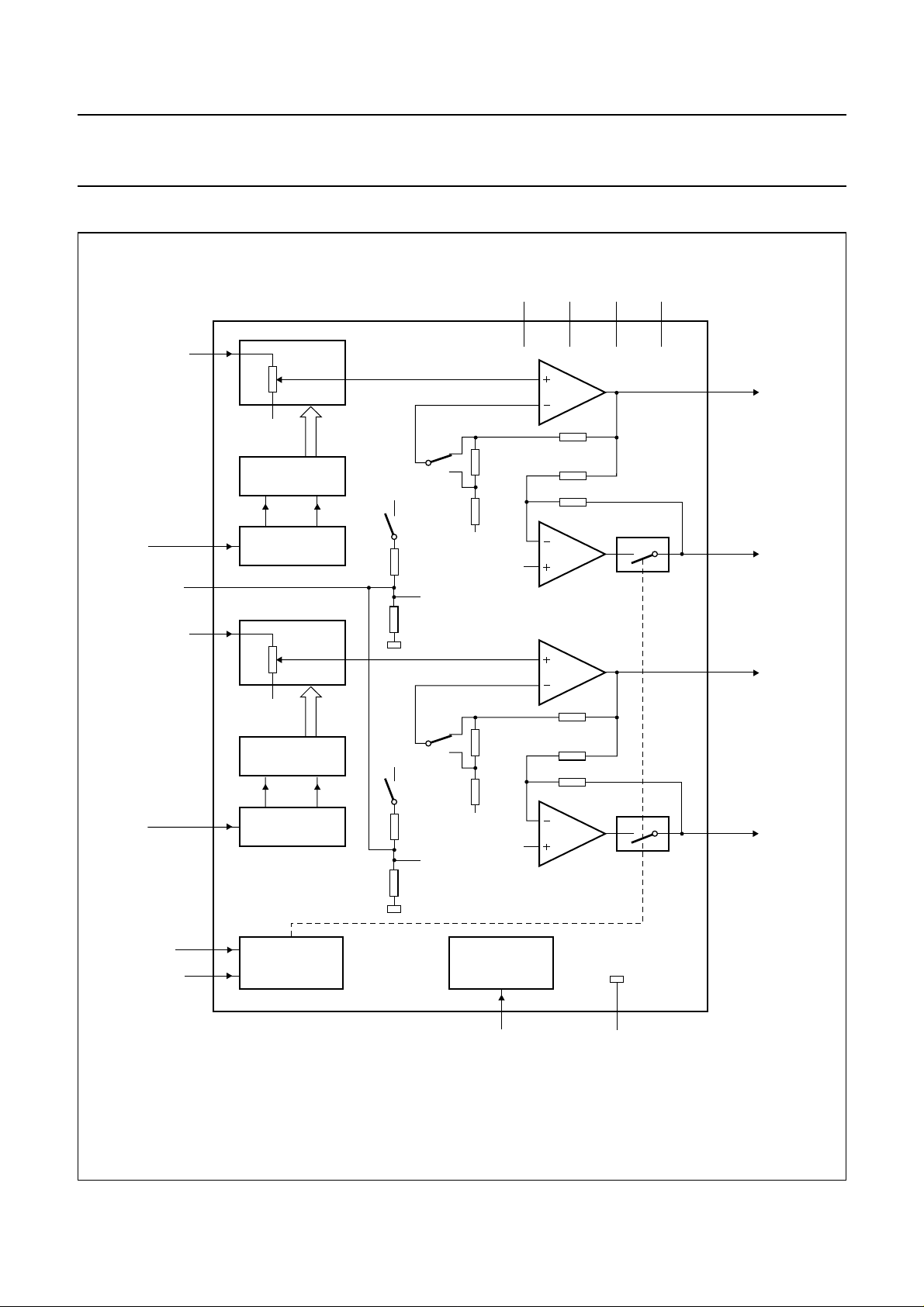
BLOCK DIAGRAM
andbook, full pagewidth
17
IN1
UP/DOWN1
SVR
IN2
6
16
15
VOLUME
CONTROL
20
kΩ
0.5V
DD
UP/DOWN
COUNTER
up down
INTERFACE
VOLUME
CONTROL
20
kΩ
20 dB
30 dB
V
DD
0.5V
DD
15 kΩ
0.5V
15 kΩ
0.5V
DD
V
DD1VDD2VDD3VDD4
381318
MASTER
15 kΩ
3.4 kΩ
1.6 kΩ
DD
20 kΩ
20 kΩ
SLAVE
TDA8552T
MASTER
12
OUT1+
19
OUT1−
2
OUT2+
UP/DOWN2
MODE
HPS
0.5V
UP/DOWN
COUNTER
7
INTERFACE
5
STANDBY/MUTE
4
AND OPERATING
DD
up down
20 dB
0.5V
DD
SELECTION
3.4 kΩ
1.6 kΩ
DD
0.5V
GAIN
V
DD
30 dB
15 kΩ
0.5V
15 kΩ
Fig.1 Block diagram.
15 kΩ
20 kΩ
20 kΩ
SLAVE
DD
1, 10, 11, 2014
GAINSEL GND1 to GND4
9
OUT2−
MGM608
2002 Jan 04 4
Philips Semiconductors Product specification
2 x 1.4 W BTL audio amplifiers with digital
volume control and headphone sensing
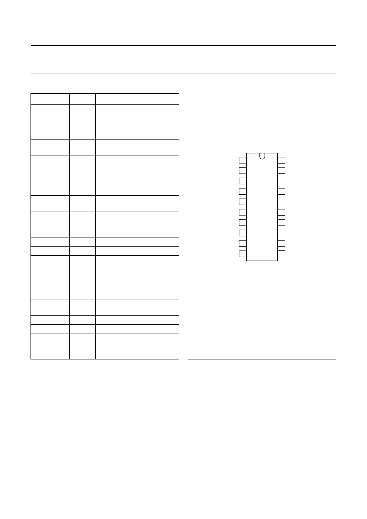
PINNING
SYMBOL PIN
GND1 1 ground 1, substrate/leadframe
OUT2+ 2 positive loudspeaker terminal
V
DD1
HPS 4 digital input for headphone
MODE 5 digital trinary input for mode
UP/DOWN1 6 digital trinary input for volume
UP/DOWN2 7 digital trinary input for volume
V
DD2
OUT2− 9 negative loudspeaker terminal
GND2 10 ground 2, substrate/leadframe
GND3 11 ground 3, substrate/leadframe
OUT1+ 12 positive loudspeaker terminal
V
DD3
GAINSEL 14 digital input for gain selection
IN2 15 audio input channel 2
SVR 16 halfsupplyvoltage, decoupling
IN1 17 audio input channel 1
V
DD4
OUT1− 19 negative loudspeaker terminal
GND4 20 ground 4, substrate/leadframe
(1)
DESCRIPTION
output channel 2
3 supply voltage 1
sensing
selection (standby, mute and
operating)
control channel 1
control channel 2
8 supply voltage 2
output channel 2
output channel 1
13 supply voltage 3
ripple rejection
18 supply voltage 4
output channel 1
handbook, halfpage
UP/DOWN1
UP/DOWN2
TDA8552T; TDA8552TS
GND1
1
OUT2+
2
V
3
DD1
HPS
4
MODE
5
TDA8552T
6
7
V
8
DD2
OUT2−
9
GND2
10
MGM610
Fig.2 Pin configuration.
20
19
18
17
16
15
14
13
12
11
GND4
OUT1−
V
DD4
IN1
SVR
IN2
GAINSEL
V
DD3
OUT1+
GND3
Note
1. For the SO20 (SOT163-1) package only: the ground
pins 1, 10, 11 and 20 are mechanically connected to
the leadframe and electrically to the substrate of the
die. On the PCB the ground pins can be connected to
a copper area to decrease the thermal resistance.
2002 Jan 04 5

Philips Semiconductors Product specification
2 x 1.4 W BTL audio amplifiers with digital
volume control and headphone sensing
FUNCTIONAL DESCRIPTION
The TDA8552T is a 2 × 1.4 W BTL audio power amplifier
capable of delivering 2 × 1.4 W output power into an 8 Ω
load at THD = 10%using a 5 V power supply. The gain of
the amplifier can be set by the digital volume control.
The gain in the maximum volume setting is 20 dB (low
gain) or 30 dB (high gain). This maximum gain can be
selected by the gain selection pin. The headphone sense
input (HPS) can be used to detect if a headphone is
pluggedinto thejack connector.If a headphoneis plugged
intothe jackconnector theamplifier switchesfrom the BTL
to the SE mode and the BTL loudspeakers are switched
off. This also results in a reduction of quiescent current
consumption. Using the MODE pin the device can be
switched to the standby condition, the mute condition or
the normal operating condition.The device is protected by
an internal thermal shutdown protection mechanism.
Power amplifier
The power amplifier is a Bridge-Tied Load (BTL) amplifier
with a complementary CMOS output stage. The total
voltage loss for both output power MOS transistors is
within 1 V and with a 5 V supply and an 8 Ω loudspeaker
an output power of 1.4 W can be delivered. The total gain
of this power amplifier can be set at 20 or 30 dB by the
gain selection pin.
Gain selection
The gain selection can be used for a fixed gain setting,
depending on the application. The gainselection pin must
be hard wired to ground (20 dB) or to VDD (30 dB). Gain
selecting during the operation is not advised, switching is
not guaranteed plop free.
Input attenuator
The volume control operates as adigitally controlled input
attenuator between the audio input pin and the power
amplifier. In the maximum volume control setting the
attenuation is 0 dB and in the minimum volume control
setting the typical attenuation is 80 dB. The attenuation
can be set in 64 steps by the UP/DOWN pin. Both
attenuators forchannels 1 and 2 are separated from each
other and are controlled by there own UP/DOWN pin.
Balance control can be arranged by applying UP/DOWN
pulses only on pins 6 and 7, see Fig.5.
TDA8552T; TDA8552TS
Volume control
Each attenuator is controlled with its own UP/DOWN pin
(trinary input):
• Floating UP/DOWN pin: volume remains unchanged
• Negative pulses: decreasing volume
• Positive pulses: increasing volume.
Each pulse on the UP/DOWN pin results in a change in
80
gain of (typical value).
In the basic application the UP/DOWN pin is switched to
ground or VDDby a double push-button. When the supply
voltage is initially connected, after a complete removal of
the supply, the initial state of the volume control is an
attenuation of 40 dB (low volume), so the gain of the total
amplifier is −20 dB in the low gain setting or −10 dB in the
high gainsetting. After powering-up, some positive pulses
have to be applied to the UP/DOWN pin for turning up to
listening volume.
Auto repeat
If the UP/DOWN pin is LOW or HIGH for the wait time (t
in seconds) (one of the keys is pressed) then the device
starts making up or down pulses by itself with a frequency
given by (repeat function).
The wait time and the repeat frequency are set using an
internal RC oscillator with an accuracy of ±10%.
Volume settings in standby mode
When the device is switched with the MODE select pin to
the mute or the standby condition, the volume control
attenuation setting keeps its value, under the assumption
that the voltage on the V
minimum supply voltage. After switching the device back
to the operation mode, the previous volume setting is
maintained. In the standby mode the volume setting is
maintained as long as the minimum supply voltage is
available. The current consumption is very low,
approximately 1 µA (typ.). In battery fed applications the
volumesetting can bemaintained during batteryexchange
if there is a supply capacitor available.
-----64
-------t
rep
1.25 dB=
wait
1
pin does not fall below the
DD
2002 Jan 04 6

Philips Semiconductors Product specification
2 x 1.4 W BTL audio amplifiers with digital
volume control and headphone sensing
Mode select pin
The deviceis in thestandby mode (with a very low current
consumption) if the voltage at the MODE pin is between
VDDandVDD− 0.5 V.At a modeselectvoltage levelofless
than 0.5 V the amplifier is fully operational. In the range
between 1 V and VDD− 1 V the amplifier is in the mute
condition.The muteconditionis usefulforusing itasa ‘fast
mute’, in this mode the output signal is suppressed, while
the volume setting remains at its value. It is advised to
keep the device in the mute condition while the input
capacitor is being charged. This can be achieved by
holding the MODE pin at a level of 0.5VDD, or by waiting
approximately 100 ms before giving the first volume-UP
pulses.
Headphone sense pin (HPS)
A headphone can beconnected tothe amplifier by using a
coupling capacitorfor each channel. The common ground
pin of the headphone is connected to the ground of the
amplifier, see Fig.4. By using the HPS pin as illustrated in
Fig.4, the TDA8552T detects if a headphone jack plug is
inserted into the connector.
TDA8552T; TDA8552TS
When noheadphone is plugged in, thevoltage level at the
HPSpin willremain LOW.A voltage lessthan VDD− 1Vat
the HPS pin will keep the device in theBTL mode,thus the
loudspeakers can be operational. If the HPS pin is not
connected then the device will remain in the BTL mode.
When a headphone is plugged into the connector, the
voltage at the HPS pin will be set to VDD. The device then
switches to the Single-Ended (SE) mode, this means that
the slave power amplifiers at the outputs OUT1− and
OUT2− will be switched to the standby mode. This results
in floating outputs OUT1− and OUT2−, the loudspeaker
signal isthus attenuated byapproximately 80 dB and only
the headphone can operate.
One of the benefits of this system is that the loudspeaker
current does not flow through the jack connector switch,
which could give some output power loss. The other
benefit is that the quiescent current is reduced when the
headphone jack is inserted.
2002 Jan 04 7
Philips Semiconductors Product specification
2 x 1.4 W BTL audio amplifiers with digital
TDA8552T; TDA8552TS
volume control and headphone sensing
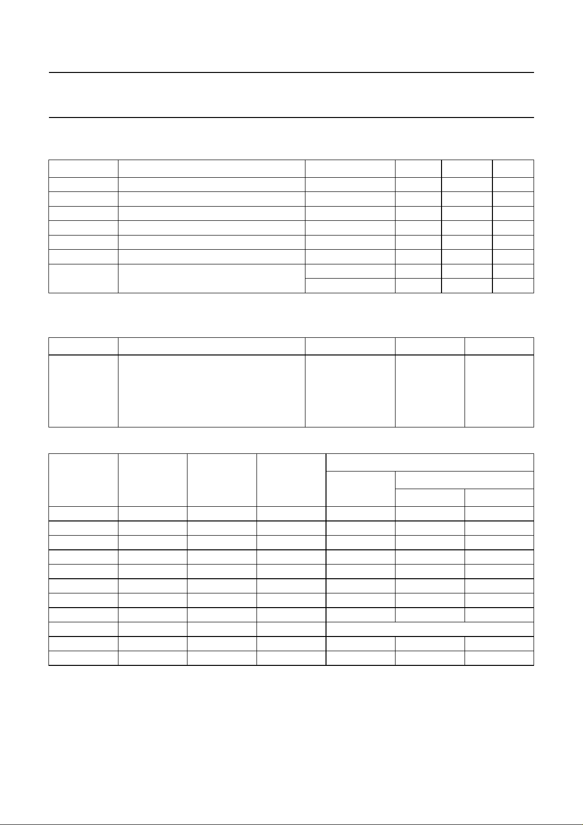
LIMITING VALUES
In accordance with the Absolute Maximum Rating System (IEC 60134).
SYMBOL PARAMETER CONDITIONS MIN. MAX. UNIT
V
DD
V
i
I
ORM
T
stg
T
amb
V
sc
P
tot
THERMAL CHARACTERISTICS
See Section “Thermal design considerations” in Chapter “Test and application information”.
SYMBOL PARAMETER CONDITIONS VALUE UNIT
R
th(j-a)
supply voltage operating −0.3 +5.5 V
input voltage −0.3 VDD+ 0.3 V
repetitive peak output current − 1A
storage temperature −55 +150 °C
operating ambient temperature −40 +85 °C
AC and DC short-circuit safe voltage − 5.5 V
maximum power dissipation SO20 − 2.2 W
SSOP20 − 1.1 W
thermal resistance from junction to ambient
for the TDA8552T (SO20) in free air 60 K/W
extra copper 55 K/W
for the TDA8552TS (SSOP20) in free air 110 K/W
extra copper 80 K/W
Table 1 Power rating; note 1
MUSIC POWER
P
V
(V) RL (Ω)
DD
o (w)
THD = 10%
OPERATION
T
P
(W)
max
amb(max)
SO20 SSOP20
3.3 4 0.9 BTL 0.55 120 106
3.3 8 0.6 BTL 0.28 134 127
3.3 16 0.3 BTL 0.14 142 139
3.3 32SE 0.035 headphone 0.03 150 150
5.0 4 2.0 BTL 1.25 81 50
5.0 8 1.4 BTL 0.65 114 98
5.0 16 0.8 BTL 0.32 132 124
5.0 32SE 0.09 headphone 0.07 146 144
continuous sine wave
3.3 4 0.9 BTL 1.1 89 62
5 8 1.4 BTL 1.25 81 50
Note
1. The power rating is based on R
with recommended copperpattern of at least 4 × 1cm2to the cornerleads and
th(j-a)
copper under the IC package.
(°C)
2002 Jan 04 8
Philips Semiconductors Product specification
2 x 1.4 W BTL audio amplifiers with digital
TDA8552T; TDA8552TS
volume control and headphone sensing
QUALITY SPECIFICATION
Quality specification in accordance with
DC CHARACTERISTICS
VDD=5V; T
=25°C; RL=8Ω; V
amb
specified.
SYMBOL PARAMETER CONDITIONS MIN. TYP. MAX. UNIT
V
DD
I
DD
I
stb
V
O
V
OUT+
− V
OUT−
supply voltage 2.7 5 5.5 V
supply current BTL mode; VDD=5V;
standby current V
DC output voltage note 2 − 2.5 − V
differential output offset
voltage
Mode select pin
V
MODE
I
MODE
α
mute
input voltage standby VDD− 0.5 − V
input current 0 < V
mute attenuation note 3 80 tbf − dB
Gain select pin
V
GAINSEL
I
GAINSEL
input voltage low gain (20 dB) 0 − 0.6 V
input current −−1µA
Headphone sense pin
V
I
HPS
HPS
input voltage SE mode; headphone
input current −−1µA
“SNW-FQ-611 part E”
= 0 V; total gain setting at 7 dB; according to Fig.4.; unless otherwise
MODE
, if this type is used as an audio amplifier.
− 14 20 mA
RL=∞; note 1
SE mode; V
BTL mode; V
=5V − 8.5 12 mA
DD
DD
= 3.3 V;
− 10 15 mA
RL= ∞; note 1
SE mode; V
MODE=VDD
= 3.3 V − 58mA
DD
− 110µA
GAINSEL=0V −−50 mV
GAINSEL = V
DD
−−150 mV
mute 1 − V
operating 0 − 0.5 V
MODE<VDD
−−1µA
high gain (30 dB) 4.1 − V
VDD− 1 − V
detected
DD
− 1.4 V
DD
DD
DD
V
V
V
2002 Jan 04 9

Philips Semiconductors Product specification
2 x 1.4 W BTL audio amplifiers with digital
TDA8552T; TDA8552TS
volume control and headphone sensing
SYMBOL PARAMETER CONDITIONS MIN. TYP. MAX. UNIT
Volume control
t
W
t
rep
V
th(up)
V
float(max)
V
float(min)
V
th(down)
I
I(up/down)
t
wait
t
rep
Volume attenuator
G
v(l)
G
v(h)
N
step
∆G
v
Z
i
V
i(max)(rms)
pulse width 50 −−ns
pulse repetition time 100 −−ns
UP/DOWN pin UP threshold
4.1 − V
DD
level
UP/DOWN pin floating high
−−3.4 V
level
UP/DOWN pin floating low
1.0 −−V
level
UP/DOWN pin DOWN
0 − 0.6 V
threshold level
input current UP/DOWN pin 0 < V
UP/DOWN<VDD
−−200 µA
auto repeat wait time − 500 − ms
repeat time key pressed − 130 − ms
low gain; maximum volume
19 20 21 dB
(including power amplifier)
low gain; minimum volume
tbf −60 tbf dB
(including power amplifier)
high gain; maximum volume
29 30 31 dB
(including power amplifier)
high gain; minimum volume
tbf −50 tbf dB
(including power amplifier)
number of gain steps − 64 −
variation of gain per step − 1.25 − dB
input impedance 14 20 − kΩ
maximum input voltage
−−1.75 V
(RMS value)
V
Notes
1. With a load connected at the outputs the quiescent current will increase, the maximum of this increase being equal
DC output offset voltage
2
to
×
----------------------------------------------------------------
R
L
2. The DC output voltage with respect to ground is approximately 0.5VDD.
3. Output voltage inmute position ismeasured with an input of1 V (RMS) in a bandwidthof 20 kHz, so including noise,
gain select pin is LOW (0 V).
2002 Jan 04 10
Philips Semiconductors Product specification
2 x 1.4 W BTL audio amplifiers with digital
TDA8552T; TDA8552TS
volume control and headphone sensing
AC CHARACTERISTICS (VDD= 3.3 V)
T
=25°C; RL=8Ω; f = 1 kHz; total gain setting at 7 dB; V
amb
(maximum gain = 20 dB); according to Fig.4.
SYMBOL PARAMETER CONDITIONS MIN. TYP. MAX. UNIT
P
o
output power THD = 10%; RL=4Ω− 0.9 − W
THD = 10%; R
THD = 10%; R
THD = 0.5%; R
THD = 0.5%; R
THD = 0.5%; R
THD total harmonic distortion P
V
o(n)
noise output voltage note 2 − 60 −µV
SVRR supply voltage ripple
= 0.1 W; note 1 − 0.1 − %
o
note 3 tbf 55 − dB
rejection
V
i(max)
maximum input voltage THD = 1%;
Gv= −50 to 0 dB
α
sup
α
cs
channel suppression V
HPS=VDD
channel separation − 55 − dB
; note 4 − 80 − dB
= 0 V; gain select pin is at 0 V
MODE
=8Ω− 0.6 − W
L
=16Ω− 0.3 − W
L
=4Ω− 0.6 − W
L
=8Ω− 0.4 − W
L
=16Ω− 0.2 − W
L
−−1.1 V
Notes
1. Volume setting at maximum.
2. The noise output voltage is measured at the output in a frequency band from 20 Hz to 20 kHz (unweighted),
R
3. Supply voltage ripple rejection is measured at the output, with a source impedance of R
=0Ω, gain select pin is LOW (0 V).
source
=0Ω at the input.
source
The ripple voltage is a sine wave with a frequency of 1 kHz and an amplitude of 100 mV (RMS) is applied to the
positive supply rail, gain select pin is LOW (0 V).
4. Channel suppression is measured at the output with a source impedance of R
=0Ω at the input and a
source
frequency of 1 kHz. The output level in the operating single-ended channel (OUT+) is set at 2 V (RMS).
2002 Jan 04 11

Philips Semiconductors Product specification
2 x 1.4 W BTL audio amplifiers with digital
TDA8552T; TDA8552TS
volume control and headphone sensing
AC CHARACTERISTICS (VDD=5V)
T
=25°C; RL=8Ω; f = 1 kHz; total gain setting at 7 dB; V
amb
(maximum gain = 20 dB); according to Fig.4; package is SO20.
SYMBOL PARAMETER CONDITIONS MIN. TYP. MAX. UNIT
P
o
output power THD = 10%; RL=8Ω 1.0 1.4 − W
THD = 10%; R
THD = 0.5%; R
THD = 0.5%; R
THD total harmonic distortion P
V
o(n)
noise output voltage GAINSEL. = 0 V; note 2 − 60 100 µV
= 0.1 W; note 1 − 0.15 0.4 %
o
= 0.5 W; note 1 − 0.1 0.3 %
P
o
GAINSEL. = V
SVRR supply voltage ripple
note 3 50 55 − dB
rejection
V
i(max)
a maximum input voltage THD = 1%;
Gv= −50 to 0 dB
α
sup
α
cs
channel suppression V
HPS=VDD
channel separation 50 −−dB
; note 4 70 80 − dB
= 0 V; Gain select pin is at 0 V
MODE
=16Ω− 0.8 − W
L
=8Ω 0.6 1.0 − W
L
=16Ω− 0.6 − W
L
; note 2 − 100 −µV
DD
−−1.75 V
Notes
1. Volume setting at maximum.
2. The noise output voltage is measured at the output in a frequency band from 20 Hz to 20 kHz (unweighted),
source
=0Ω.
=0Ω at the input.
source
R
3. Supply voltage ripple rejection is measured at the output, with a source impedance of R
The ripple voltage is a sine wave with a frequency of 1 kHz and an amplitude of 100 mV (RMS) is applied to the
positive supply rail, gain select pin is LOW (0 V).
4. Channel suppression is measured at the output with a source impedance of R
=0Ω at the input and a
source
frequency of 1 kHz. The output level in the operating single-ended channel (OUT+) is set at 1 V (RMS).
2002 Jan 04 12

Philips Semiconductors Product specification
2 x 1.4 W BTL audio amplifiers with digital
TDA8552T; TDA8552TS
volume control and headphone sensing
AC CHARACTERISTICS (FOR HEADPHONE; RL=32Ω; CONNECTED SE)
V
=5V; T
DD
(maximum gain = 20 dB); according to Fig.4.
SYMBOL PARAMETER CONDITIONS MIN. TYP. MAX. UNIT
P
o
THD total harmonic distortion P
V
o(n)
SVRR supply voltage ripple
V
i(max)
α
cs
Notes
1. The noise output voltage is measured at the output in a frequency band from 20 Hz to 20 kHz (unweighted),
R
source
2. Supply voltage ripple rejection is measured at the output, with a source impedance of R
The ripple voltage is a sine wave with a frequency of 1 kHz and an amplitude of 100 mV (RMS) is applied to the
positive supply rail, gain select pin is LOW (0 V).
=25°C; f = 1 kHz; total gain setting at 20 dB; V
amb
output power THD = 10%; VDD= 3.3 V − 35 − mW
THD = 10%; V
THD = 0.5%; V
THD = 0.5%; V
=60mW − 0.04 − %
o
noise output voltage note 1 − 60 100 µV
note 2 50 55 − dB
rejection
maximum input voltage THD = 1%;
Gv= −50 to 0 dB
channel separation 50 −−dB
=0Ω, gain select pin is LOW (0 V).
= 0 V; gain select pin is 0 V
MODE
= 5.0 V − 90 − mW
DD
= 3.3 V − 25 − mW
DD
= 5.0 V − 60 − mW
DD
−−1.75 V
=0Ω at the input.
source
handbook, full pagewidth
t
V
DD
V
th(UP)
V
float(max)
V
UP/DOWN
V
float(min)
V
th(DOWN)
0
The rise time (tr) of the pulse may have any value.
r
t
rep
t
w
decreasing volume
t
Fig.3 Timing UP/DOWN pin.
2002 Jan 04 13
increasing volume
floating
t
r
t
rep
t
w
MGM611

Philips Semiconductors Product specification
2 x 1.4 W BTL audio amplifiers with digital
volume control and headphone sensing
TEST AND APPLICATION INFORMATION
handbook, full pagewidth
C1
17
volume
control
volume
control
IN1
330 nF
V
IN1
V
DD
up
R5
2.2 kΩ
down
V
DD
up
down
C7
R6
2.2 kΩ
mute
100
nF
V
V
330 nF
IN2
C8
100 nF
DD
standby
operating
UP/DOWN1
C3
220 µF
C2
UP/DOWN2
MODE
SVR
IN2
HPS
6
16
15
7
5
4
VOLUME
CONTROL
20
kΩ
0.5V
DD
UP/DOWN
COUNTER
up down
INTERFACE
VOLUME
CONTROL
20
kΩ
0.5V
DD
UP/DOWN
COUNTER
up down
INTERFACE
STANDBY/MUTE
AND OPERATING
20 dB
30 dB
V
DD
15 kΩ
0.5V
15 kΩ
20 dB
V
DD
30 dB
15 kΩ
0.5V
15 kΩ
V
0.5V
DD
0.5V
DD
DD
V
DD1, 2
3, 8 13, 18
MASTER
15 kΩ
3.4 kΩ
1.6 kΩ
DD
0.5V
20 kΩ
20 kΩ
SLAVE
DD
TDA8552T
MASTER
15 kΩ
3.4 kΩ
1.6 kΩ
DD
0.5V
GAIN
SELECTION
20 kΩ
20 kΩ
SLAVE
DD
GAINSEL GND1 to GND4
TDA8552T; TDA8552TS
VDD = 5 V
V
DD3, 4
12
19
2
9
1, 10, 11, 2014
R3
100 kΩ
C3 C4
OUT1+
220 µF
8 Ω
OUT1−
OUT2+
8 Ω
OUT2−
V
DD
R2
820 kΩ
100
nF
C5
C6
220 µF
220 µF
R1
1 kΩ
headphone jack
tip
ring
sleeve
R4
1 kΩ
ground
MGM609
Fig.4 Test and application diagram.
2002 Jan 04 14

Philips Semiconductors Product specification
2 x 1.4 W BTL audio amplifiers with digital
volume control and headphone sensing
Test conditions
T
=25°C if not specially mentioned; VDD=5V;
amb
f = 1 kHz, R
22 Hz to 22 kHz.Thethermal resistance (instandardprint,
without extra copper) = 110 K/W for the SSOP20; the
maximum sine wave power dissipation is:
150 25–
---------------------110
For T
amb
150 60–
---------------------110
Thermal design considerations
The ‘measured’ thermal resistance of the IC package is
highly dependent on the configuration and size of the
application board. All surface mount packages rely on the
traces of the PCB to conductheat awayfrom thepackage.
To improve the heat flow, a significant area on the PCB
must be attached to the (ground) pins. Data may not be
comparable between different semiconductor
manufacturers because the application boards and test
methods are not (yet) standardized. Also, the thermal
performance of packagesfor aspecific applicationmay be
differentthan presented here,because theconfigurationof
the application boards (copper area) may be different.
PhilipsSemiconductors uses FR-4typeapplication boards
with 1 oz copper traces with solder coating Solder Resist
Mask (SRM).
The SSOP20 package has improved thermal conductivity
which reduces the thermal resistance. Using a practical
PCB layout (see Fig.18) with wider copper tracks to the
corner pins and just under the IC, the thermal resistance
from junction to ambient can be reduced to approximately
80 K/W. For T
dissipation for this PCB layout is:
The thermal resistance for the SO20 is approximately
55 K/W if applied to a PCBwith wider copper tracks to the
corner pins and just under the body of the IC.
The maximum total power dissipation for this practical
application is:
150 60–
----------------------
55
=8Ω, Gv= 20 dB, audio band-pass
L
1.14 W=
=60°C the maximum total power dissipation is:
0.82 W=
=60°C the maximum total power
amb
150 60–
---------------------80
1.63 W=
1.12 W=
TDA8552T; TDA8552TS
BTL application
The BTL application diagram is illustrated in Fig.4.
The quiescent current has been measured without any
load impedance. The total harmonic distortion as a
function of frequency was measured with a low-pass filter
of 80 kHz. The value of capacitor C3 influences the
behaviour of the SVRR at low frequencies, increasing the
value of C3 increases the performance of the SVRR.
Headphone application
=25°C if not specially mentioned, VDD=5V,
T
amb
f = 1 kHz, RL=32Ω, Gv= 14 dB, audio band-pass
22 Hz to 22 kHz.
For headphone application diagram see: Fig.4
If a headphone is plugged into the headphone jack, the
HPS pin will switch-off the outputs of the SLAVE output
stage, this results in a mute attenuation >80 dB for the
loudspeakers. In this condition the quiescent current will
be reduced.
General remarks
Reduction of the value of capacitor C3 results in a
decrease of the SVRR performance at low frequencies.
The capacitor value of C5 and C6 in combination with the
load impedance of the headphone determines the low
frequency behaviour.
To prevent against high output currents during inserting
the headphone into theheadphone jack,resistors of5.1 Ω
have to be connected in series with the SE output lines.
The UP/DOWNpin can be driven by a 3-statelogic output
stage (microprocessor) without extra external
components. If the UP/DOWN pin is driven by
push-buttons, then it is advised to have an RC-filter
between the buttons and the UP/DOWN pin. Advised
valuesfor the RC-filterare2.2 kΩ and100 nF. Resistor R4
is not necessary for basic operation, but is advised to
keep C6 charged to a voltage of 0.5VDD This has the
advantage that the plop noise when inserting the
headphone plug is minimal. If the headphone sense
function (HPS) is not used then the HPS-pin 4 should be
hard-wired to ground. This pin should never be left
unconnected.
Using double push buttons, the volume step for both
channels can be controlled. When for the balance control
only a single contact is used, the balance steps are
1.25 dB. If double contacts are used for the balance
buttons and the dashed connection is made, then the
balance steps are 2.5 dB.
2002 Jan 04 15

Philips Semiconductors Product specification
2 x 1.4 W BTL audio amplifiers with digital
TDA8552T; TDA8552TS
volume control and headphone sensing
Application without volume control
If pins 6, 7 and 8 are hardwired together the device operates with the volume control setting at maximum.
When the supply voltage is connectedand thedevice isswitched fromstandby tomute or operating for the first time then
the gain is ramped up from −20 dB to +20 dB. This takes approximately 5 s.
This maximum gain setting is maintained until the supply voltage drops below the minimum value.
V
V
DD
DD
balance left
volume
down
up
2.2 kΩ
UP/DOWN1
100 nF
6
TDA8552T
2.2 kΩ
UP/DOWN2
100 nF
7
MGM612
handbook, full pagewidth
V
DD
balance right
Fig.5 Volume and balance control using buttons.
2002 Jan 04 16
Philips Semiconductors Product specification
2 x 1.4 W BTL audio amplifiers with digital
volume control and headphone sensing
5
MGR005
VDD (V)
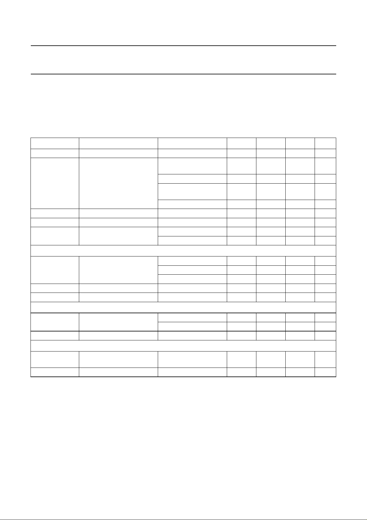
20
handbook, halfpage
I
DD
(mA)
15
10
5
0
234 6
RL= ∞.
40
handbook, halfpage
G
(dB)
20
0
−20
−40
−60
02040 80
VDD= 5 V; RL=8Ω.
(1) Gv= 30 dB (max.).
(2) Gv= 20 dB (max.).
TDA8552T; TDA8552TS
MGR006
(1)
(2)
60
volume steps
Fig.6 IDD as a function of VDD.
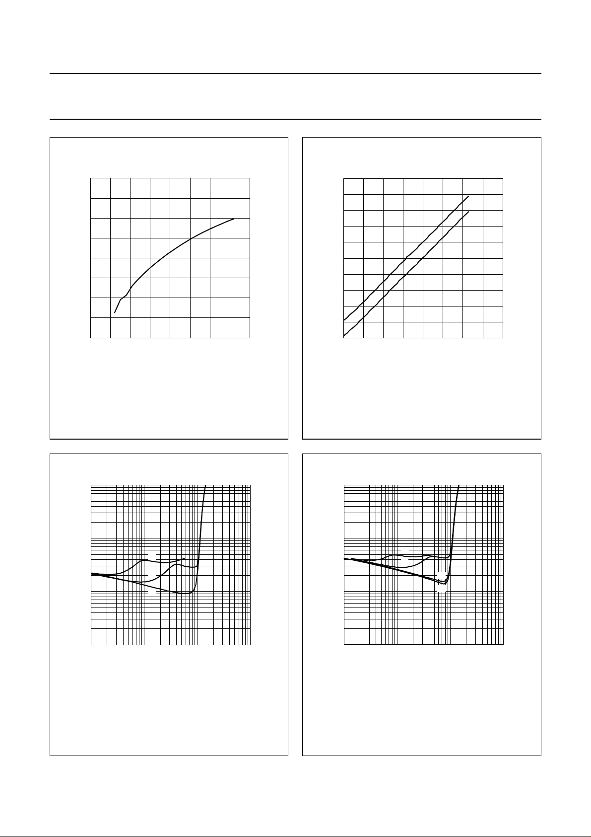
10
handbook, halfpage
THD
(%)
1
(1)
(2)
−1
10
−2
10
−2
10
VDD= 5 V; RL=8Ω; f = 1 kHz; Gv= 20 dB (max.).
(1) Gv= 0 dB.
(2) Gv= 7 dB.
(3) Gv= 20 dB.
(3)
−1
10
MGR007
110
Po (W)
Fig.7 Gain as a function of volume steps.
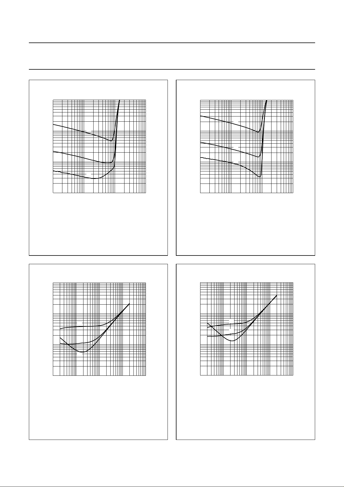
10
handbook, halfpage
THD
(%)
1
(1)
(2)
(3)
−1
10
−2
10
−2
10
VDD= 5 V; RL=8Ω; f = 1 kHz; Gv= 30 dB (max.).
(1) Gv= 0 dB.
(2) Gv= 7 dB.
(3) Gv=20dB.
(4) Gv=30dB.
−1
10
(4)
MGR008
110
Po (W)
Fig.8 THD as a function of Po.
2002 Jan 04 17
Fig.9 THD as a function of Po.
Philips Semiconductors Product specification
2 x 1.4 W BTL audio amplifiers with digital
volume control and headphone sensing
10
handbook, halfpage
THD
(%)
1
−1
10
−2
10
−2
10
(1)
(2)
(3)
−1
10
VDD= 5 V; RL=8Ω; Gv= 20 dB (max.).
(1) f = 10 kHz.
(2) f = 1 kHz.
(3) f = 100 Hz.
110
MGR009
Po (W)
TDA8552T; TDA8552TS
10
handbook, halfpage
THD
(%)
1
−1
10
−2
10
−2
10
VDD= 5 V; RL=8Ω; Gv= 30 dB (max.).
(1) f = 10 kHz.
(2) f = 1 kHz.
(3) f = 100 Hz.
(1)
(2)
(3)
−1
10
MGR010
110
Po (W)
Fig.10 THD as a function of Po.
10
handbook, halfpage
THD
(%)
1
(1)
−1
10
−2
10
10 10
VDD= 5 V; RL=8Ω; Po= 0.1 W; Gv= 20 dB (max.).
(1) Gv= 0 dB.
(2) Gv= 7 dB.
(3) Gv= 20 dB.
(2)
(3)
2
3
10
Fig.11 THD as a function of Po.
MGR011
10
handbook, halfpage
THD
(%)
1
(1)
(2)
−1
10
−2
4
10
f (Hz)
5
10
10
10 10
(3)
2
3
10
VDD= 5 V; RL=8Ω; Po= 0.1 W; Gv= 30 dB (max.).
(1) Gv= 0 dB.
(2) Gv= 7 dB.
(3) Gv=30dB.
MGR012
4
10
f (Hz)
5
10
Fig.12 THD as a function of frequency.
2002 Jan 04 18
Fig.13 THD as a function of frequency.

Philips Semiconductors Product specification
2 x 1.4 W BTL audio amplifiers with digital
volume control and headphone sensing
MGR013
4
10
f (Hz)
5
10
SVRR
0
(1)
handbook, halfpage
(dB)
(2)
−20
(3)
(4)
−40
(5)
(6)
−60
−80
10 10
VDD= 5 V; RL=8Ω; V
(1) C3 = 10 µF; Gv=20dB.
(2) C3 = 10 µF; Gv= 7 dB.
(3) C3 = 100 µF; Gv= 20 dB.
(4) C3 = 10 µF; Gv=10dB.
(5) C3 = 100 µF; Gv= 7 dB.
(6) C3 = 100 µF; Gv= 10 dB.
2
= 100 mV.
ref
3
10
TDA8552T; TDA8552TS
2.4
handbook, halfpage
V
i
(V)
2
1.6
1.2
0.8
0.4
0
−50 −30 −10
VDD= 5 V; RL=8Ω; f = 1 kHz; THD = 1%.
(1) Gv= 20 dB (max.).
(2) Gv= 30 dB (max.).
MGR014
(1)
(2)
G (dB)
30
100
Fig.14 SVRR as a function of frequency.
handbook, halfpage
0
α
sup
(dB)
−20
−40
−60
−80
−100
10
VP= 5 V; Vo= 1 V; V
(1) Channel 1.
(2) Channel 2.
2
10
HPS=VP
Fig.15 Input voltage as a function of gain.
MGL436
handbook, halfpage
α
(dB)
0
cs
−20
−40
−60
(1)
(2)
3
10
4
10
f (Hz)
5
10
.
−80
−100
10
VP= 5 V; Vo=1V.
2
10
(1)
(2)
3
10
(1) Gv=30dB.
(2) Gv=20dB.
MGL435
4
10
f (Hz)
5
10
Fig.16 Channel suppression as a function of
frequency.
2002 Jan 04 19
Fig.17 Channel separation as a function of
frequency.

Philips Semiconductors Product specification
2 x 1.4 W BTL audio amplifiers with digital
volume control and headphone sensing
handbook, full pagewidth
TDA8552T; TDA8552TS
77
79
top view
IN1
330 nF
330 nF
IN2
20 dB
30 dB
TDA
8552/53TS
Analog Audio
CIC – Nijmegen
220 µF
100 nF
MODE
20 1
150 nF
220 µF
TDA8552/53TS
1 kΩ
− OUT1 +− OUT2 +
+VddGND
100 kΩ
220 µF
220 µF
820
kΩ
1.5 kΩ
5 Ω
bottom view
1.5 kΩ
UP
DOWN
HP
5 Ω
1 kΩ
MGR015
Fig.18 Printed-circuit board layout.
2002 Jan 04 20

Philips Semiconductors Product specification
2 x 1.4 W BTL audio amplifiers with digital
volume control and headphone sensing
PACKAGE OUTLINES
SO20: plastic small outline package; 20 leads; body width 7.5 mm
D
c
y
Z
20
11
TDA8552T; TDA8552TS
SOT163-1
E
H
E
A
X
v M
A
pin 1 index
1
e
0 5 10 mm
DIMENSIONS (inch dimensions are derived from the original mm dimensions)
mm
A
max.
2.65
0.10
A
0.30
0.10
0.012
0.004
1
A2A
2.45
2.25
0.096
0.089
0.25
0.01
b
0.49
0.36
p
cD
0.32
0.23
0.013
0.009
3
0.019
0.014
UNIT
inches
Note
1. Plastic or metal protrusions of 0.15 mm maximum per side are not included.
10
w M
b
p
scale
(1)E(1) (1)
13.0
12.6
0.51
0.49
eHELLpQ
7.6
1.27
7.4
0.30
0.050
0.29
10.65
10.00
0.419
0.394
Q
A
2
A
1
1.4
0.055
1.1
0.4
0.043
0.016
detail X
1.1
1.0
0.043
0.039
(A )
L
p
L
0.25
0.01
A
3
θ
0.25 0.1
0.01
ywv θ
Z
0.9
0.4
8
0.004
0.035
0.016
0
o
o
OUTLINE
VERSION
SOT163-1
IEC JEDEC EIAJ
075E04 MS-013
REFERENCES
2002 Jan 04 21
EUROPEAN
PROJECTION
ISSUE DATE
97-05-22
99-12-27

Philips Semiconductors Product specification
2 x 1.4 W BTL audio amplifiers with digital
volume control and headphone sensing
SSOP20: plastic shrink small outline package; 20 leads; body width 4.4 mm
20
D
c
y
Z
11
E
H
E
TDA8552T; TDA8552TS
SOT266-1
A
X
v M
A
pin 1 index
110
w M
b
e
DIMENSIONS (mm are the original dimensions)
mm
A
max.
1.5
0.1501.4
1.2
2
A3b
0.25
p
0.32
0.20
UNIT A1A
Note
1. Plastic or metal protrusions of 0.20 mm maximum per side are not included.
p
0 2.5 5 mm
cD
0.20
6.6
0.13
6.4
(1)E(1)
4.5
4.3
scale
eHELLpQZywv θ
0.65 1.0 0.2
6.6
6.2
Q
A
2
A
1
detail X
0.75
0.65
0.45
0.45
(A )
L
p
L
A
3
θ
0.13 0.1
0.48
0.18
(1)
o
10
o
0
OUTLINE
VERSION
SOT266-1 MO-152
IEC JEDEC EIAJ
REFERENCES
2002 Jan 04 22
EUROPEAN
PROJECTION
ISSUE DATE
95-02-22
99-12-27

Philips Semiconductors Product specification
2 x 1.4 W BTL audio amplifiers with digital
volume control and headphone sensing
SOLDERING
Introduction to soldering surface mount packages
Thistext givesa verybrief insight toa complex technology.
A more in-depth account of soldering ICs can be found in
our
“Data Handbook IC26; Integrated Circuit Packages”
(document order number 9398 652 90011).
There is no soldering method that is ideal for all surface
mount IC packages. Wave soldering can still be used for
certainsurface mount ICs,but it isnotsuitable forfine pitch
SMDs. In these situations reflow soldering is
recommended.
Reflow soldering
Reflow soldering requires solder paste (a suspension of
fine solder particles, flux and binding agent) to be applied
tothe printed-circuitboard by screenprinting, stencillingor
pressure-syringe dispensing before package placement.
Several methods exist for reflowing; for example,
convection or convection/infrared heating in a conveyor
type oven. Throughput times (preheating, soldering and
cooling) vary between 100 and 200 seconds depending
on heating method.
Typical reflow peak temperatures range from
215 to 250 °C. The top-surface temperature of the
packages should preferable be kept below 220 °C for
thick/large packages, and below 235 °C for small/thin
packages.
Wave soldering
Conventional single wave soldering is not recommended
forsurface mount devices(SMDs) or printed-circuitboards
with a high component density, as solder bridging and
non-wetting can present major problems.
To overcome these problems the double-wave soldering
method was specifically developed.
TDA8552T; TDA8552TS
• Use a double-wave soldering method comprising a
turbulent wavewith high upwardpressure followed by a
smooth laminar wave.
• For packages with leads on two sides and a pitch (e):
– larger than or equal to 1.27 mm, the footprint
longitudinal axis is preferred to be parallel to the
transport direction of the printed-circuit board;
– smaller than 1.27 mm, the footprint longitudinal axis
must be parallel to the transport direction of the
printed-circuit board.
The footprint must incorporate solder thieves at the
downstream end.
• Forpackages with leadson four sides,thefootprint must
be placedat a 45° angle to the transportdirection of the
printed-circuit board. The footprint must incorporate
solder thieves downstream and at the side corners.
During placement and before soldering, thepackage must
be fixed with a droplet of adhesive. The adhesive can be
applied by screen printing, pin transfer or syringe
dispensing. The package can be soldered after the
adhesive is cured.
Typical dwell time is 4 seconds at 250 °C.
A mildly-activated flux will eliminate the need for removal
of corrosive residues in most applications.
Manual soldering
Fix the component by first soldering two
diagonally-opposite end leads. Use a lowvoltage (24 V or
less) soldering iron applied to the flat part of the lead.
Contact time must be limited to 10 seconds at up to
300 °C.
When using a dedicated tool, all other leads can be
soldered in one operation within 2 to 5 seconds between
270 and 320 °C.
If wave soldering is used the following conditions must be
observed for optimal results:
2002 Jan 04 23

Philips Semiconductors Product specification
2 x 1.4 W BTL audio amplifiers with digital
TDA8552T; TDA8552TS
volume control and headphone sensing
Suitability of surface mount IC packages for wave and reflow soldering methods
PACKAGE
BGA, HBGA, LFBGA, SQFP, TFBGA not suitable suitable
HBCC, HLQFP, HSQFP, HSOP, HTQFP, HTSSOP, HVQFN, SMS not suitable
(3)
PLCC
LQFP, QFP, TQFP not recommended
SSOP, TSSOP, VSO not recommended
Notes
1. All surface mount (SMD) packages are moisture sensitive. Depending upon the moisture content, the maximum
2. These packages are not suitable for wave soldering. On versions with the heatsink on the bottom side, the solder
3. If wave soldering is considered, then the package must be placed at a 45° angle to the solder wave direction.
4. Wave soldering is only suitable for LQFP, TQFP and QFP packages with a pitch (e) equal to or larger than 0.8 mm;
5. Wave soldering isonly suitable forSSOP and TSSOP packages witha pitch (e) equal toor larger than 0.65 mm; it is
, SO, SOJ suitable suitable
temperature (with respect to time) and body size of the package, there is a risk that internal or external package
cracks may occur due to vaporization of the moisture in them (the so called popcorn effect). For details, refer to the
Drypack information in the
cannot penetrate between the printed-circuit board and the heatsink. On versions with the heatsink on the top side,
the solder might be deposited on the heatsink surface.
The package footprint must incorporate solder thieves downstream and at the side corners.
it is definitely not suitable for packages with a pitch (e) equal to or smaller than 0.65 mm.
definitely not suitable for packages with a pitch (e) equal to or smaller than 0.5 mm.
“Data Handbook IC26; Integrated Circuit Packages; Section: Packing Methods”
SOLDERING METHOD
WAVE REFLOW
(2)
(3)(4)
(5)
suitable
suitable
suitable
(1)
.
2002 Jan 04 24

Philips Semiconductors Product specification
2 x 1.4 W BTL audio amplifiers with digital
TDA8552T; TDA8552TS
volume control and headphone sensing
DATA SHEET STATUS
PRODUCT
DATA SHEET STATUS
Objective data Development This data sheet contains data from the objective specification for product
Preliminary data Qualification This data sheet contains data from the preliminary specification.
Product data Production This data sheet contains data from the product specification. Philips
Notes
1. Please consult the most recently issued data sheet before initiating or completing a design.
2. The product status of the device(s) described in this data sheet may have changed since this data sheet was
published. The latest information is available on the Internet at URL http://www.semiconductors.philips.com.
(1)
STATUS
(2)
development. Philips Semiconductors reserves the right to change the
specification in any manner without notice.
Supplementary data will be published at a later date. Philips
Semiconductors reserves the right to change the specification without
notice, in order to improve the design and supply the best possible
product.
Semiconductors reserves the right to make changes at any time in order
to improve the design, manufacturing and supply. Changes will be
communicated according to the Customer Product/Process Change
Notification (CPCN) procedure SNW-SQ-650A.
DEFINITIONS
DEFINITIONS
Short-form specification The data in a short-form
specification is extracted from a full data sheet with the
same type number and title. For detailed information see
the relevant data sheet or data handbook.
Limiting values definition Limiting values given are in
accordance with the Absolute Maximum Rating System
(IEC 60134). Stress above one or more of the limiting
values may cause permanent damage to the device.
These are stress ratings only and operation of the device
atthese oratany otherconditionsabove thosegivenin the
Characteristics sectionsof the specification is not implied.
Exposure to limiting values for extended periods may
affect device reliability.
Application information Applications that are
described herein for any of these products are for
illustrative purposes only. Philips Semiconductors make
norepresentation or warrantythatsuch applicationswill be
suitable for the specified use without further testing or
modification.
DISCLAIMERS
Life support applications These products are not
designed for use in life support appliances, devices, or
systems where malfunction of these products can
reasonably be expectedto resultin personalinjury. Philips
Semiconductorscustomers using orsellingthese products
for use in such applications do so at their own risk and
agree to fully indemnify Philips Semiconductors for any
damages resulting from such application.
Right to make changes Philips Semiconductors
reserves the right to make changes, without notice, in the
products, including circuits, standard cells, and/or
software, described or contained herein in order to
improve design and/or performance. Philips
Semiconductors assumes no responsibility or liability for
theuse of anyof these products,conveysno licenceor title
under any patent, copyright, or mask work right to these
products,and makesnorepresentations orwarranties that
these products are free from patent, copyright, or mask
work right infringement, unless otherwise specified.
2002 Jan 04 25

Philips Semiconductors Product specification
2 x 1.4 W BTL audio amplifiers with digital
volume control and headphone sensing
NOTES
TDA8552T; TDA8552TS
2002 Jan 04 26

Philips Semiconductors Product specification
2 x 1.4 W BTL audio amplifiers with digital
volume control and headphone sensing
NOTES
TDA8552T; TDA8552TS
2002 Jan 04 27

Philips Semiconductors – a w orldwide compan y
Contact information
For additional information please visit http://www.semiconductors.philips.com. Fax: +31 40 27 24825
For sales offices addresses send e-mail to: sales.addresses@www.semiconductors.philips.com.
© Koninklijke Philips Electronics N.V. 2002
All rights are reserved. Reproduction in whole or in part is prohibited without the prior written consent of the copyright owner.
The information presented in this document does not form part of any quotation orcontract, is believed to be accurate and reliable and may be changed
without notice. No liability will be accepted by the publisher for any consequence of its use. Publication thereof does not convey nor imply any license
under patent- or other industrial or intellectual property rights.
Printed in The Netherlands 753503/03/pp28 Date of release: 2002 Jan 04 Document order number: 9397 750 09236
SCA74
 Loading...