

Page 1
.HIGH SPEED
tPD= 6 ns (TYP.) AT VCC=5V
.LOWPOWER DISSIPATION
ICC=1 µA (MAX.) AT TA=25°C
.HIGH NOISEIMMUNITY
V
NIH=VNIL
=28%VCC(MIN.)
.OUTPUT DRIVE CAPABILITY
10 LSTTL LOADS
.SYMMETRICAL OUTPUT IMPEDANCE
IOH =IOL= 4 mA(MIN.)
.BALANCEDPROPAGATION DELAYS
t
PLH=tPHL
.WIDE OPERATINGVOLTAGERANGE
VCC(OPR)= 2 V TO 6 V
.PIN AND FUNCTION COMPATIBLE WITH
54/74LS04
M54HC04
M74HC04
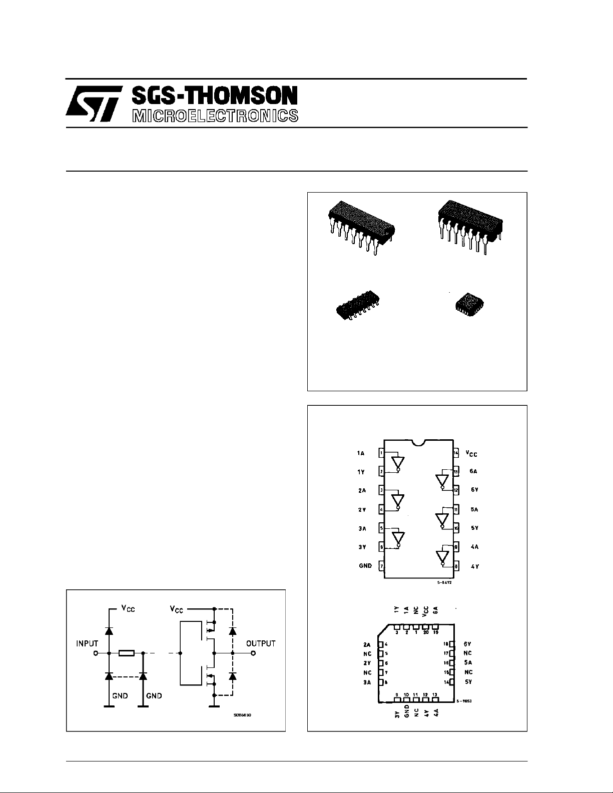
HEX INVERTER
B1R
(PlasticPackage)
M1R
(MicroPackage)
ORDER CODES :
M54HC 04F1R M74H C04M1R
M74HC 04B1R M 74HC04C1R
(CeramicPackage)
(Chip Carrier)
F1R
C1R
DESCRIPTION
The M54/74HC04 is a highspeed CMOS HEX INVERTERfabricated in silicon gate C2MOS technology. It has the same high speed performance of
LSTTL combined with true CMOS low power consumption.
The internal circuit is composedof 3 stages including buffer output, which enables high noise immunity and stable output. All inputs are equipped
with circuits against static discharge and transient
excess voltage.
INPUT AND OUTPUT EQUIVALENT CIRCUIT
PIN CONNECTIONS(top view)
NC =
No Internal
Connection
December1992
1/9
Page 2
M54/M74HC04
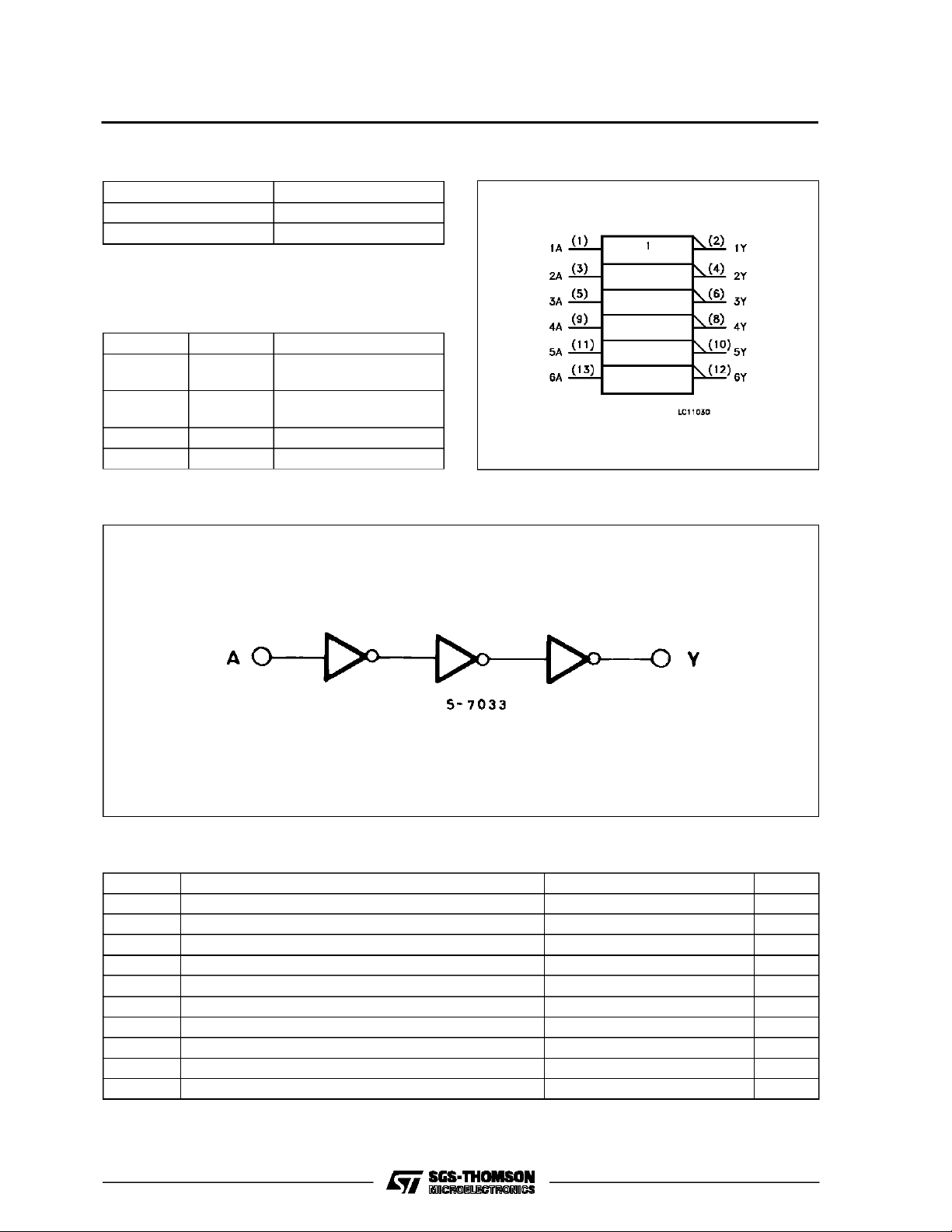
TRUTH TABLE
AY
LH
HL
PIN DESCRIPTION
PIN No SYMBOL NAME AND FUNCTION
1, 3, 5, 9,
1A to 6A Data Inputs
11, 13
2, 4, 6, 8,
1Y to 6Y Data Outputs
10, 12
7 GND Ground (0V)
14 V
CC
Positive Supply Voltage
LOGI C DI AG RAM (Pe r Gate)
IEC LOGIC SYMBOL
ABSOLU TE MAXI MU M RAT INGS
Symbol Parameter Value Unit
V
CC
V
V
O
I
IK
I
OK
I
O
or I
I
CC
P
D
T
stg
T
L
AbsoluteMaximumRatingsarethosevalues beyondwhichdamagetothedevicemayoccur. Functionaloperationunder theseconditionisnotimplied.
(*)500 mW: ≅ 65oC derate to300 mW by 10mW/oC: 65oCto85oC
2/9
Supply Voltage -0.5 to +7 V
DC Input Voltage -0.5 to VCC+ 0.5 V
I
DC Output Voltage -0.5 to VCC+ 0.5 V
DC Input Diode Current ± 20 mA
DC Output Diode Current ± 20 mA
DC Output Source Sink Current Per Output Pin ± 25 mA
DC VCCor Ground Current ± 50 mA
GND
Power Dissipation 500 (*) mW
Storage Temperature -65 to +150
Lead Temperature (10 sec) 300
o
C
o
C
Page 3

M54/M74HC04
RECO MM ENDED OPERATIN G C O NDITI ONS
Symbol Parameter Value Unit
V
V
V
T
t
r,tf
DC SPECIFICA TIONS
Symbol Parameter
V
IH
V
V
OH
V
OL
I
I
CC
Supply Voltage 2 to 6 V
CC
Input Voltage 0 to V
I
Output Voltage 0 to V
O
Operating Temperature: M54HC Series
op
M74HC Series
CC
CC
-55 to +125
-40 to +85
Input Rise and Fall Time VCC= 2 V 0 to 1000 ns
V
= 4.5 V 0 to 500
CC
V
= 6 V 0 to 400
CC
Test Conditions Value
V
(V)
CC
=25oC
T
A
54HC and 74HC
-40 to 85oC
74HC
-55 to 125oC
Min. Typ. Max. Min. Max. Min. Max.
High Level Input
Voltage
2.0 1.5 1.5 1.5
4.5 3.15 3.15 3.15
6.0 4.2 4.2 4.2
Low Level Input
IL
Voltage
2.0 0.5 0.5 0.5
4.5 1.35 1.35 1.35
6.0 1.8 1.8 1.8
High Level
Output Voltage
Low Level Output
Voltage
Input Leakage
I
Current
Quiescent Supply
2.0
V
=
I
4.5 4.4 4.5 4.4 4.4
6.0 5.9 6.0 5.9 5.9
4.5 I
6.0 I
2.0
4.5 0.0 0.1 0.1 0.1
6.0 0.0 0.1 0.1 0.1
4.5 I
6.0 I
6.0
IO=-20 µA
V
IH
or
V
IL
=-4.0 mA 4.18 4.31 4.13 4.10
O
=-5.2 mA 5.68 5.8 5.63 5.60
O
V
=
I
IO=20µA
V
IH
or
V
IL
= 4.0 mA 0.17 0.26 0.33 0.40
O
= 5.2 mA 0.18 0.26 0.33 0.40
O
VI=VCCor GND ±0.1 ±1 ±1 µA
1.9 2.0 1.9 1.9
0.0 0.1 0.1 0.1
6.0 VI=VCCor GND 1 10 20 µA
Current
54HC
V
V
o
C
o
C
Unit
V
V
V
V
3/9
Page 4

M54/M74HC04
AC ELECTRICAL CHARACTERISTICS (CL=50pF,Inputtr=tf=6ns)
Test Conditions Value
T
=25oC
Symbol Parameter
t
t
TLH
THL
Output Transition
Time
V
CC
(V)
2.0 30 75 95 110
4.5 8151922
A
54HC and 74HC
Min. Typ. Max. Min. Max. Min. Max.
6.0 7131619
t
PLH
t
PHL
Propagation
Delay Time
2.0 27 75 95 110
4.5 9151922
6.0 8131619
C
C
PD
Input Capacitance 5 10 10 10 pF
IN
(*) Power Dissipation
22
Capacitance
(*) CPDisdefined asthe valueof the IC’s internalequivalent capacitance whichiscalculated from the operating current consumption withoutload.
(Referto TestCircuit).Average operting currentcan be obtained bythe followingequation. ICC(opr) = CPD•VCC•fIN+ICC/6(per Gate)
SWITCHING CHARACTERISTICS TEST CIRCUIT
-40 to 85oC
74HC
-55 to 125oC
54HC
Unit
ns
ns
pF
TEST CIRCUIT ICC(Opr.)
INPUTWAVEFORMIS THE SAMEASTHAT INCASE OF SWITCHINGCHARACTERISTICSTEST.
4/9
Page 5

Plastic DIP14 MECHANICAL DATA
M54/M74HC04
DIM.
MIN. TYP. MAX. MIN. TYP. MAX.
a1 0.51 0.020
B 1.39 1.65 0.055 0.065
b 0.5 0.020
b1 0.25 0.010
D 20 0.787
E 8.5 0.335
e 2.54 0.100
e3 15.24 0.600
F 7.1 0.280
I 5.1 0.201
L 3.3 0.130
Z 1.27 2.54 0.050 0.100
mm inch
P001A
5/9
Page 6

M54/M74HC04
Ceramic DIP14/1 MECHANICAL DATA
DIM.
MIN. TYP. MAX. MIN. TYP. MAX.
A 20 0.787
B 7.0 0.276
D 3.3 0.130
E 0.38 0.015
e3 15.24 0.600
F 2.29 2.79 0.090 0.110
G 0.4 0.55 0.016 0.022
H 1.17 1.52 0.046 0.060
L 0.22 0.31 0.009 0.012
M 1.52 2.54 0.060 0.100
N 10.3 0.406
P 7.8 8.05 0.307 0.317
Q 5.08 0.200
mm inch
6/9
P053C
Page 7

SO14 MECHANICAL DATA
M54/M74HC04
DIM.
MIN. TYP. MAX. MIN. TYP. MAX.
A 1.75 0.068
a1 0.1 0.2 0.003 0.007
a2 1.65 0.064
b 0.35 0.46 0.013 0.018
b1 0.19 0.25 0.007 0.010
C 0.5 0.019
c1 45° (typ.)
D 8.55 8.75 0.336 0.344
E 5.8 6.2 0.228 0.244
e 1.27 0.050
e3 7.62 0.300
F 3.8 4.0 0.149 0.157
G 4.6 5.3 0.181 0.208
L 0.5 1.27 0.019 0.050
M 0.68 0.026
S8°(max.)
mm inch
P013G
7/9
Page 8

M54/M74HC04
PLCC20 MECHANICAL DATA
DIM.
MIN. TYP. MAX. MIN. TYP. MAX.
A 9.78 10.03 0.385 0.395
B 8.89 9.04 0.350 0.356
D 4.2 4.57 0.165 0.180
d1 2.54 0.100
d2 0.56 0.022
E 7.37 8.38 0.290 0.330
e 1.27 0.050
e3 5.08 0.200
F 0.38 0.015
G 0.101 0.004
M 1.27 0.050
M1 1.14 0.045
mm inch
8/9
P027A
Page 9

M54/M74HC04
Information furnished is believed to be accurate and reliable. However, SGS-THOMSON Microelectronics assumes no responsability for the
consequences of use of such information nor for any infringement of patents or other rights of third parties which may results from its use. No
license is grantedbyimplication or otherwise under any patent or patent rights ofSGS-THOMSONMicroelectronics. Specificationsmentioned
in this publication are subject to change without notice. This publication supersedes and replaces all information previously supplied.
SGS-THOMSON Microelectronicsproductsare notauthorized foruse ascritical componentsinlife support devices orsystems without express
written approval of SGS-THOMSON Microelectonics.
1994 SGS-THOMSON Microelectronics - All Rights Reserved
Australia - Brazil - France - Germany - Hong Kong - Italy - Japan - Korea - Malaysia - Malta - Morocco - The Netherlands -
Singapore - Spain - Sweden - Switzerland - Taiwan - Thailand - UnitedKingdom - U.S.A
SGS-THOMSON Microelectronics GROUP OF COMPANIES
9/9
 Loading...