

Page 1
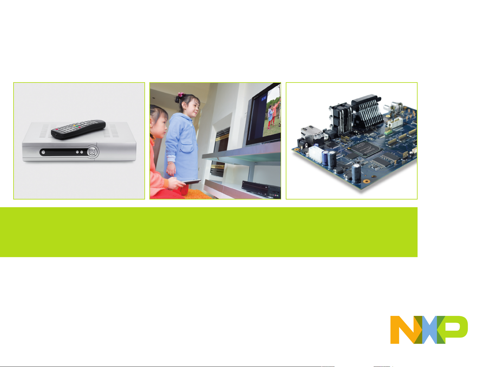
Application guide
Set-top boxes (STBs)
Page 2

Contents
Your partner for STBs 3
1. Power solutions 4
1.1 AC/DC controllers
1.2 Discretes
2. RF reception stage 6
2.1 Silicon tuners (cable, satellite, terrestrial)
2.2 LNA and loop-through switches
3. Analog audio and video interfaces 8
3.1 Audio digital-to-analog converters (DACs)
3.2 Audio and video switches
3.3 ESD protection for AV interfaces
(SCART, YC, YPbPr, Audio L/R, RGB, VGA)
4. HDMI interface 13
4.1 HDMI transmitters
4.2 HDMI switch
4.3 CEC controller
4.4 DDC and CEC buffers
4.5 ESD protection
6. Data transfer interfaces: ESD protection 22
6.1 ESD protection for USB
6.2 ESD protection for USB 3.0
6.3 ESD protection for SATA, eSATA
6.4 ESD protection for Ethernet
6.5 ESD protection and EMI ltering for SD card
and other low/medium-speed interfaces
7. Interfaces and control 26
7.1 Microcontrollers
7.2 I2C GPIO expanders
7.3 I2C temperature sensors
7.4 I2C level shifters
7.5 I2C bridges (SPI, UART) and 16C-compatible UARTs
7.6 I2C real-time clocks (RTCs)
7.7 I2C design tools and tech support
7.8 Logic functions
7.9 Memory termination regulator
8. Discrete components for 34
the main processing board
8.1 Power solutions
8.2 Special functions and general-purpose devices
Additional resources 36
5. Smart-card reader interface 18
2
Page 3
Introduction
Your partner for STBs
NXP Semiconductors offers a wide portfolio of advanced solutions for set-top-boxes (STBs).
All are built on our deep understanding of what network operators and manufacturers need.
We can deliver application-specific solutions for reception, drawing on a complete range of
silicon tuners that cover all the major standards for satellite, terrestrial, and cable reception.
We also support peripheral functions, such as advanced audio and HDMI interfaces, and
provide an extensive portfolio of standard products for STBs.
We use next-generation packaging to save space, lower costs, and improve AV content
security, and we reduce energy consumption with low-power technologies that dramatically
increase efficiency. We design for ruggedness, supplying devices that stand up to intensive
use, and we deliver the high integration needed to simplify development, lower BOM and
production costs, and reduce time-to-market.
We are known for innovation and our ability to introduce new technologies that set the
standard for performance, efficiency, and size. Our new chip-scale package (CSP) devices,
for example, have an exceptionally compact footprint yet achieve a new benchmark in
mechanical robustness.
We support our customers with a cost-efficient supply chain, and an enterprise-wide
commitment to the highest standards of security, quality, and reliability. We also help our
customers prepare for the future, by working with them to implement new features, such
as 3D, that will drive growth. In short, our customers have the confidence that comes from
working with a world-class partner.
There’s more.
This application guide provides an introduction to our STB portfolio. It highlights many of
the forward-thinking solutions we have available, but it’s only the beginning. To learn more,
please visit our dedicated application page at www.nxp.com/applications/set_top_box/.
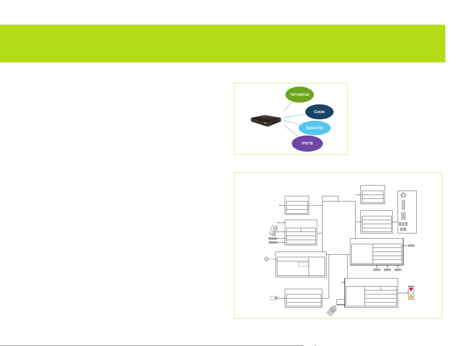
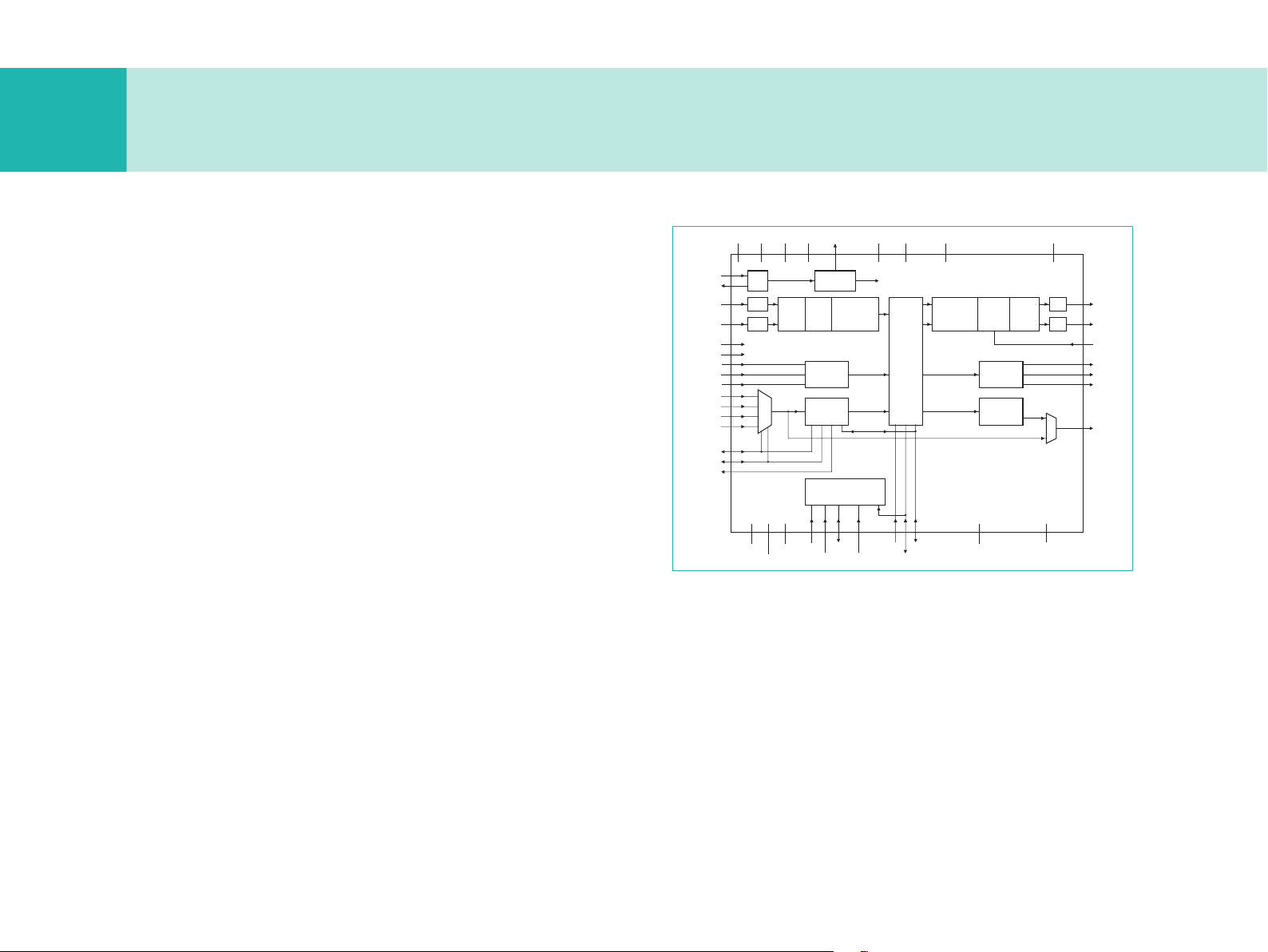
NXP supports all the existing STB standards
NXP improves performance throughout the system
WiFi, ethernet
hard-disk
drive
USB
USB 3.0
from
sat/cable/terr
IC card or CI
PCMCIA
RS232
UART
SATA
eSATA
LOOP-THROUGH SWITCH
SAT OR CABLE OR
TERRESTRIAL TUNER
module
LOW SPEED I/F
RS232
UART
LOGIC
MEMORY, STORAGE AND
COMMUNICATION I/F
FLASH SDRAM
ESD PROTECTION
DDR TERMINATOR
LOGIC
RF INPUT INTERFACE
LNA
CHANNEL
DECODER
CONTENT ACCESS CONTROL
ESD PROTECTION
IC CARD READER
LOGIC
DISCRETES
STB MAIN
PROCESSOR
key pad
IR
mains
TRANSMITTER
SYSTEM MANAGEMENT, POWER
MANAGEMENT, HUMAN INTERFACE
UC
POWER
DC-DC
POWER SUPPLY
DISCRETES
AUDIO VIDEO OUTPUTS
ESD PROTECTION
AUDIO DAC
VIDEO SWITCH
AUDIO SWITCH
DIGITAL AV INTERFACE
ESD PROTECTION
HDMI
CEC CONTROLLER
HDMI HDMI HDMI
PLL
BUS CONTROLLER
LOGIC
TEMP SENSOR
HDMI SWITCH
DDC BUFFER
HDMI RECEIVER
RTC
GPIO
brb540
AV outputs
S-VHS
SCART
VGA
YPbPr
L/R
HDMI
signalling
3
Page 4
1. Power solutions
We specialize in saving power, and build on decades of expertise in
portable and battery-powered systems. Our GreenChip family, now in its
third generation, delivers best-in-class efficiency for power supplies, and our
broad portfolio of discretes help optimize power consumption throughout
the system.
1.1 AC/DC controllers
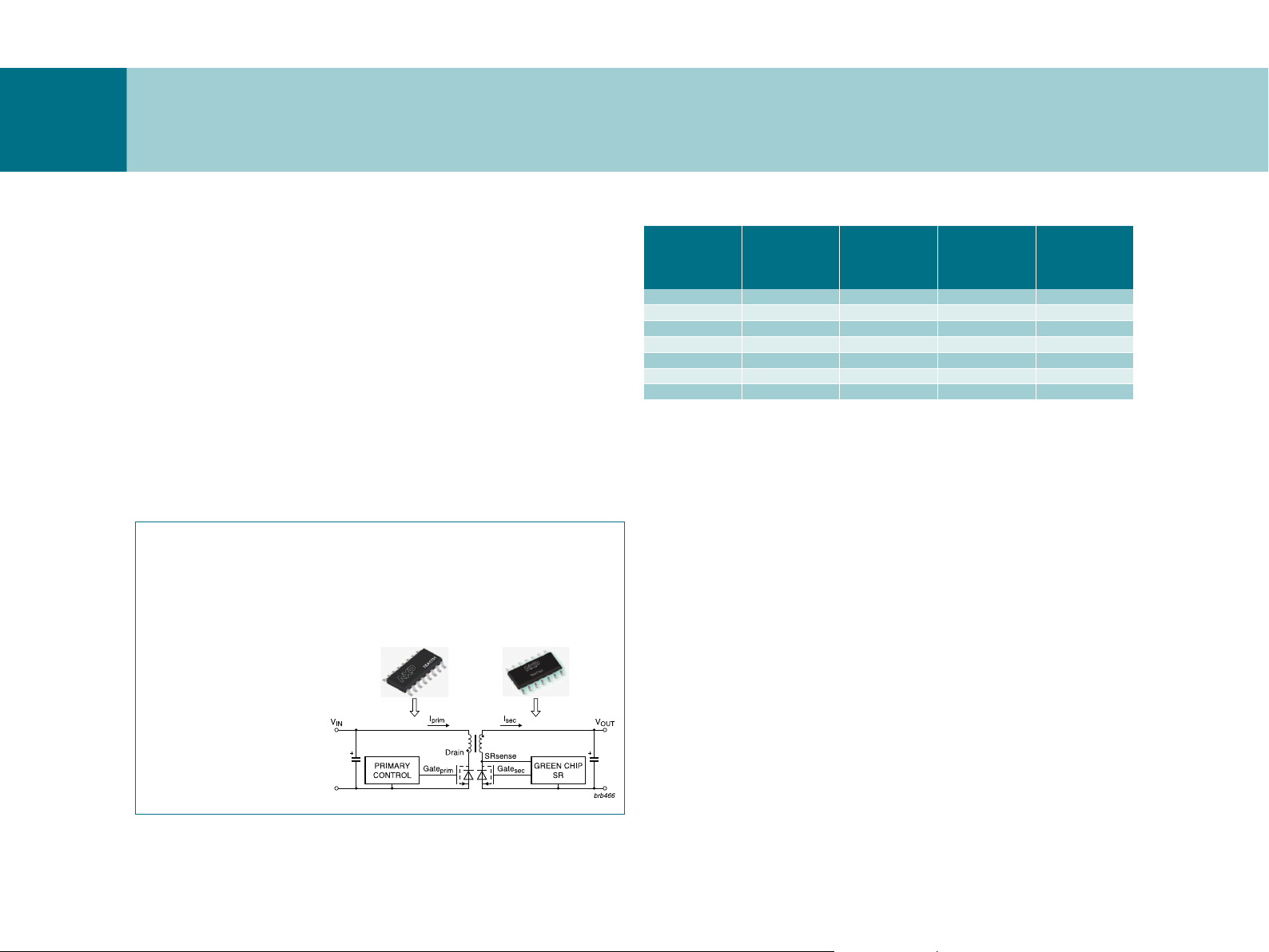
High-power GreenChip family TEA175x(L) and GreenChip SR family
TEA176x & TEA179x
Designed for switched-mode power supplies (SMPS), NXP’s extremely
efficient and highly integrated GreenChip ICs enable simple, cost-effective
power supplies with very few external components.
GreenChip III / SR: Flyback converters
TEA1571, TEA1752, TEA1761, TEA1762, TEA1791
• GEN3 SMPS controller & SR IC delivers
high efciency at all power levels
• Energy STAR V 2.0 compliant (87% eff.)
• Allows small adapter form factors
• High integration reduces external
component count, lowers overall cost
• Reduced design-in time with easy
controlled start-up behavior and V
• Special built-in green functions,
e.g. PFC switches off during stand-by,
lowload
• Standby power reduced by 100 mW
compared to conventional PFC solutions
• Minimizes losses on secondary side by
as much much as 5 W (rectifying diode
replaced by switch and smart controller IC)
• High protection level
Low-power STARplug family TEA152x
For simple STBs that use a power supply of less than 20 W (often called
“zapper” STBs), our STARplug family of SMPS ICs is the best fit.
cc
mngt
Type number Package R
TEA1520T/N2 SO-14 48 2 - 5 W Standby supply
TEA1520P/N2 DIP-8 48 2 - 5 W Standby supply
TEA1521T/N2 SO-14 24 3 - 7 W Standby s upply
TEA1521P/N2 DIP-8 24 3 - 7 W Standby supply
TEA1522T/N2 SO-14 12 7 - 9 W Stand by supp ly
TEA1522P/N2 DIP-8 12 7 - 9 W Standby supply
TEA1523P/N2 DIP-8 6.5 9 - 12 W Standby supply
DSon
Max output
power on
global mains
Application
example
>30 W SMPS IC TEA1733
Supporting power higher than 30 W, the TEA1733 is an ideal solution for
high-end STBs with multiple options (such as HDD for recording), and highend gateways that concentrate content reception at the home input.
Features
SMPS controller IC enabling low-cost applications
Large input voltage range (12 to 30 V)
Very low supply current during start-up and restart (10 μA typ)
Low supply current during normal operation (0.5 mA typ without load)
Over-power or high/low line compensation
Adjustable over-power time-out
Adjustable over-power restart timer
Fixed switching frequency with frequency jitter to reduce EMI
Frequency reduction with fixed minimum peak current to maintain high-
efficiency at low output power levels
Slope compensation for CCM operation
Low and adjustable over-current protection (OCP) trip level
Adjustable soft-start operation
Two protection inputs (e.g. for input UVP and OVP, OTP and output OVP)
IC over-temperature protection
4
Page 5
1. Power solutions
1.2 Discretes
The power consumption of STBs and other consumer appliances is
progressively going down, because of new efficiency requirements
and new power conservation regulations. This trend, among other
factors, enables the usage of our new medium power Schottky diodes
in the AC/DC 12 V rail.
Our medium power Schottky diodes in SOD123W and SOD128
packages are used as freewheeling diodes on the secondary side,
with an operating range of 30 to 60 V and 1 to 5 A. Recommended
products include PMEG6030EP and PMEG4050EP.
• Our TL431xxFDT series offer enhanced EMI ruggedness, an
outstanding step response, and stability area for all SMPS
applications.
Schot tky
diodes
PMEG403 0ER SOD123W BZX84 J-SERIES SOD323F
PMEG4050EP SOD128
PMEG6030EP SOD128 BZX84 -SERIES SOT23 TL431XXFDT SOT23(SC74)
Zener diodes Analog ICs
5
Page 6
2. RF reception stage
2.1 Silicon tuners
Our portfolio covers digital STBs for cable, satellite, and terrestrial
reception. We offer flexible platform development, whether the
system is being optimized for low cost or high performance. The
portfolio includes single and multiple tuners with optional loop-through
circuitry (but without external splitters), as well as the possibility
One product can be used for several designs, including cable and
terrestrial formats, and our software drivers simplify design work even
further. All our tuners deliver excellent performance and are suitable
for high-end analog/digital applications. Also, our products have been
validated against major standards worldwide.
to use several tuners in parallel for multistream viewing/recording.
NXP silicon tuners
Worldwide coverage • DVB-S, DVB-S2, DVB-C, DVB- C2, DVB-T, DVB-T2, ATSC A74, ISDB-T, DTMB, and more
Fully integrated • LNA, RF & Filters, Loo p Throu gh circ uitr y, RF split ters, and more
High perfor mance • Noise figure, AGC, maximum inp ut level, phase noise, image rejec tion, ACI, CSO, CTB, etc.
Validate d reference designs • ATSC A74, NorDig, CENELEC, DTG, and others
• More t han 1 billion MOPLL and IF ICs sold
Robus t technology
• Rigorous lab and fiel d testing
• Customer test-c ase validation
• System valid ation with par tners
Recommended tuners for cable STBs
Part number Europe China USA 1 GHz MOCA Filter Dual tuner Multiple tuner out Loop through
TDA18250
TDA18252
TDA18253
TDA18254A
TDA18260
• •
• • • •
• • • • •
• • • • • • •
• • • • • • • •
Recommended tuners for satellite STBs
Part number DVB-S DVB-S2 Single tuner Dual tuner Loop-through circuitry
CX24113A Yes No Yes No No No No
CX24118A Yes Yes Yes No No No No
CX24132 Yes Yes No Yes No No No
TDA20136 Yes Yes No Yes Yes Yes No
TDA20142 Yes Yes Yes No Yes No Yes
LNA splitter &
RF switch
FTA LNA
Recommended tuners for terrestrial STBs
Part number
TDA18218
TDA18219
TDA18212
DVB-T
•
•
•
DVB-T2 ATSC ISDB-T/DTMB Cable compliant 2nd tuner output Loop through
No
Ok
Best
• • • • •
• • •
•
6
Page 7
2. RF reception stage
2.2 LNA and loop-through switches
LNA BGU703x
For applications that require sensitivity and noise figure beyond what’s
already integrated into NXP’s high-performance silicon tuners, an
external LNA from the BGU703x series can be used in front of the tuner.
BGU703x series
BGU7031 LNA wit h fixed g ain
BGU7032 LNA wit h fixed g ain and bypass m ode
BGU7033 LNA wit h two gain levels and bypass mode
STB tuner
RF in
RF switch
BF11x8
RF out to TV
TV
LNAfilter
LNA
brb533
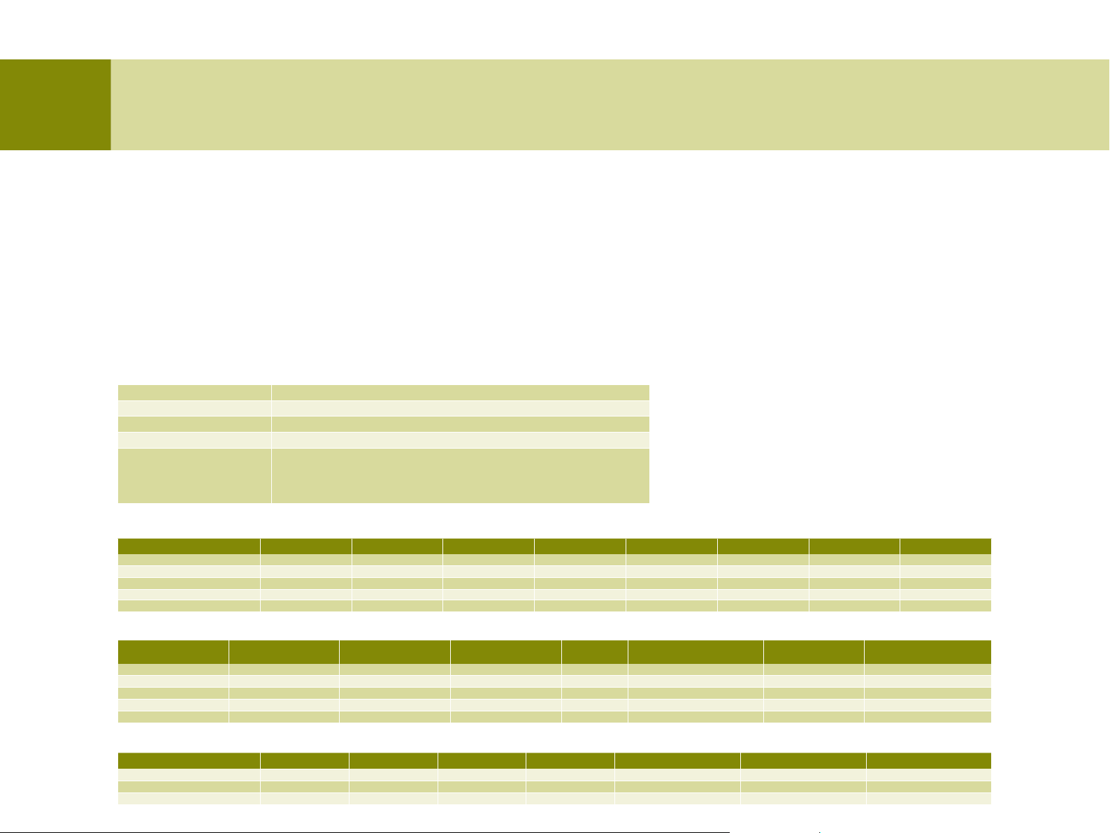
Silicon RF switch and MOSFET BF1108 and BF1118
NXP’s silicon tuners offer built-in loop-through functionality in standby
mode. Depending on the power requirements of the intended system,
designers may choose to implement the loop-through function outside
the tuner, using an external part. In this case, the BF1108/BF1118 is
the recommended solution. It lets the TV connection operate, without
quality loss, even when the STB is turned off. It is a depletion-type FET
and a band-switching diode in a single SOT143B package. Low loss and
high isolation provide excellent RF switching functions. The MOSFET
gate can be isolated from ground with the diode, resulting in low
losses. Integrated diodes between gate and source and between gate
and drain protect against excessive input voltage surges. The BF1108
operates at 5 V while the BF1118 is for designs using 3.3 V supply.
Features
Specially designed for low-loss RF switching up to 1 GHz
Easy to design-in
Power ON: high isolation (switch is open)
Power OFF: low losses (switch is closed)
ON or OFF, ZERO power consumption
7
Page 8
3. Analog audio and video interfaces
3.1 Audio digital-to-analog
converters (DACs)
We offer a wide range of stereo DACs with serial inputs. The UDA133x
series uses the I2S interface, the UDA1352TS supports SPDIF formats,
and the UDA1355 is ideal for designs that require very complex audio
I/O schemes.
Audio DAC series UDA133x
Type Supply PLL Volume control Control Data formats Package
UDA1330ATS 2.7 to 5.5 V Digi tal logarithm I2C / L3 / Static
UDA1334ATS 2.4 to 3.6 V • Static
UDA1334BTS 2.4 to 3.6 V Static SSOP16
UDA1334BT 2.4 to 3.6 V Static SO16
2
I
S, LSB, or MSB justified;
16, 18, 20, 24 bit; 1 F
2
I
S, LSB justified;
16, 18, 20, 24 bit; 1 F
s
s
SSOP16
SSOP16
PLL0
PLL
DAC
NOISE SHAPER
DAC
V
DDA
V
O(L)
V
O(R)
V
V
REF
SSA
brb534
BCK
DATA1
SYSCLK/PLL1
MUTE
DEEM/CLKOUT
WS
SFOR1 SFOR0
DIGITAL INTERFACE
FILTER
DE-EMPHASES
INTERPOLATION
V
DDDVSSD
Audio DAC UDA1352TS
Type Output Control
UDA1352TS Stereo L3/I2C 5th 256 f s • • • • 40- bit dB Lin
Noise
shaper
Sys
clock
PLL
PCM
detec t
SPDIF
lock
AC-3/MPEG
detec t
Ch
status
Vol
control
DAC DSP Data formats Package
Anti- plop
Auto mute
Bass boost,
treble
IEC958 (SPDIF);
28 to 100 kHz
SSOP28
8
Page 9
3. Analog audio and video interfaces
Audio codec UDA1355
An SPDIF codec for systems that require very complex audio I/O schemes.
Features
2.4 to 3.6 V supply voltage
SPDIF I/O codec
• 4 SPDIF inputs by select switch
• 1 SPDIF output
• Stereo analog I/O
I2C / L3 control and static mode of operation
Mixing features for 2 data streams
ADC with volume control -63.5 to 24 dB
DAC with sound processing
• Left/right volume control: -78 to 0 dB
• Left/right bass boost and treble control
• Optional resonant bass boost control
Multiple operating modes
• SPDIF to I2C to SPDIF + analog
• Analog to I2C to SPDIF
• SPDIF to analog
XTALIN
XTALOUT
VINR
RESET
RTCB
DATAI
BCKI
SPDIF0
SPDIF1
SPDIF2
SPDIF3
SLICER_SEL0
SLICER_SEL1
LOCK
TIMING
PROCESSOR
CONTROL
INTERFACE
MP2
AUDIO
FEATURE
SEL_STATIC
V
DDIVREFVDDE
INPUT
AND
OUTPUT
SELECT
MODE2
MODE0
MODE1
AUDIO
FEATURE
PROCESSOR
V
SSE
INTER-
POLATOR
DATA OUT
IEC 60958
ENCODER
UDA1355H
NOISE
SHAPER
V
DDA1
40
VOUTL
DAC
42
VOUTR
DAC
44
MUTE
9
WSO
8
DATAO
10
BCKO
5
SPDIFOUT
41
mgu826
V
SSA1
V
V
DDX
SSXVADCPVDDA2
12
15
13
XTAL
14
34
VINL
ADC
36
ADC
16
43
2
WSI
3
1
SLICER
23
24
25
26
21
22
4
33 35 28
V
ADCN
V
SSA2
CLK_OUT
32 37 27 38 6 3911
CLOCK AND
COMB
DECI-
FILTER
MATOR
DATA IN
IEC 60958
DECODER
29 30 31 20 17 18 19 7
V
SSIS
MP0
MP1
9
Page 10

3. Analog audio and video interfaces
3.2 Audio and video switches
These switches support multiplexing and demultiplexing of analog
audio and video signals (including HD and UXGA) without signal
degradation.
Quad 5 V 2-1 video mux/demux NX5DV330
This single 5 V analog switch (4PCO/4PTT) supports a bandwidth of 300
MHz and offers 5 Ω on resistance. It is available in SO, SSOP, TSSOP,
and DQFN packages.
Low-ohmic audio switches NX3LXXXX
These switches can be used to connect the STB’s SoC to multiple
selectable connectors on the back panel, such as SCART, Y/C, and
YPbPr connections.
Features
Low-ohmic, on resistance RON <1.0 Ω for minimal signal attenuation
-90 dB isolation and crosstalk for superior signal integrity
Low current consumption for higher power savings
Low RON / CON combination adds performance and flexibility:
• Digital data switching in portable applications
• Analog functions in audio applications
• Audio and data multiplexing around interface
7.5 kV ESD performance or better
Built-in “translator/level shifter” function (“T” models only)
• interfaces more easily with low voltage ASIC applications
• reduces component count
Smallest footprint: PicoGate and MicroPak packages with 0.35 mm pitch
10
Page 11
3. Analog audio and video interfaces
3.3 ESD protection for analog AV
interfaces
We offer discrete and integrated ESD protection devices for all the audio
and video interfaces commonly used by an STB, so it’s easy to find the
right configuration for a given application layout.
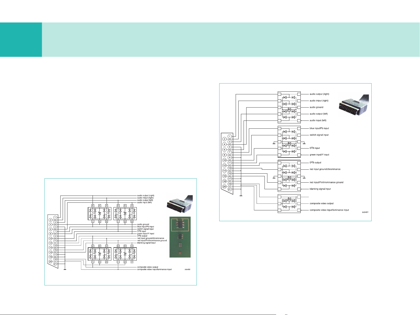
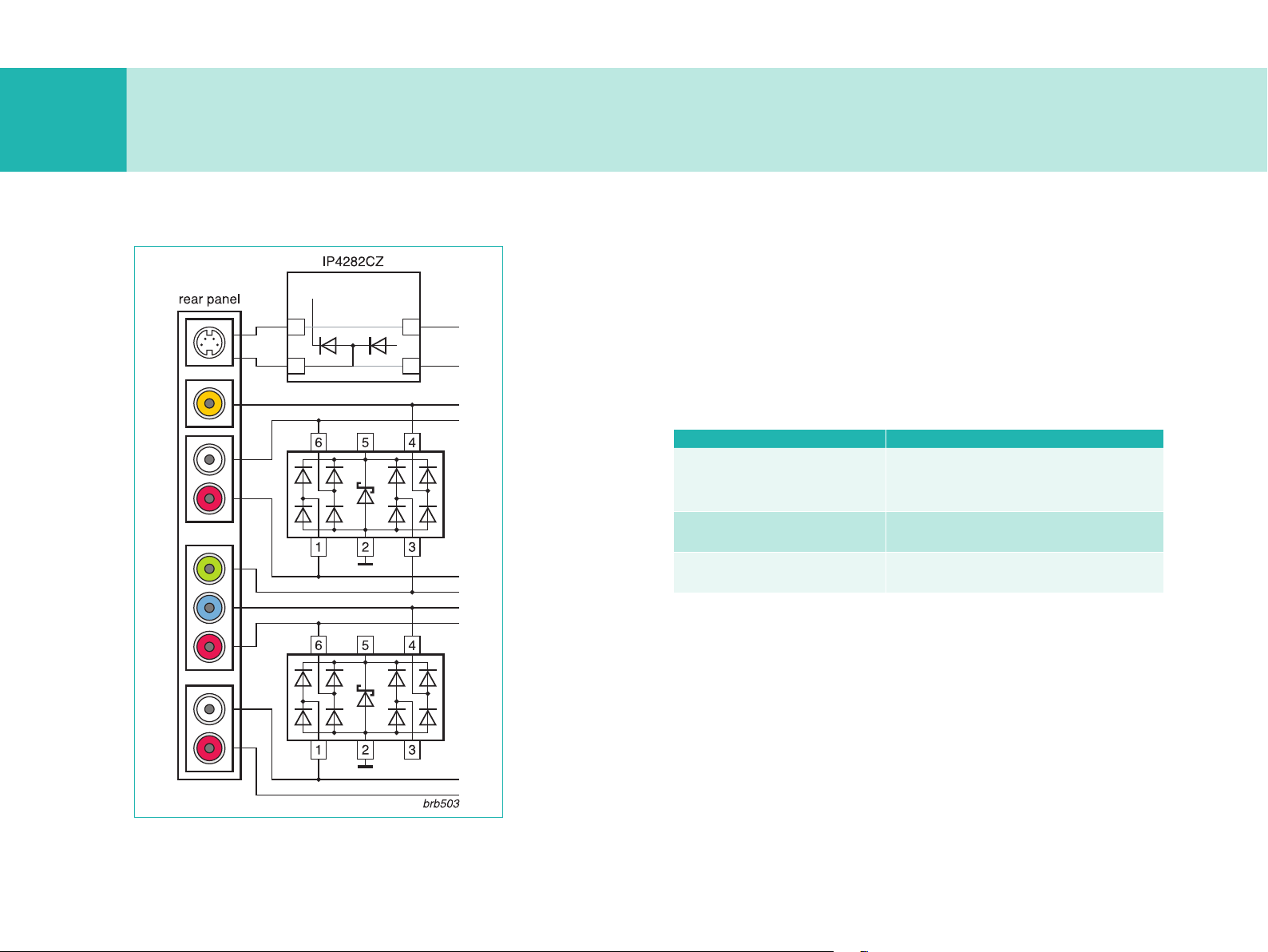
ESD protection for SCART
As shown in the diagrams, the IP4220CZ6 and the IP4221-S/XS can be
used to protect SCART signals, as can the IP4283CZ10 and IP4282CZ6.
Other configurations are also possible.
IP4220CZ6 and IP4221-S/XS configuration
IP4283CZ10 and IP4282CZ6 configuration
ESD protection for YC, YPbPr, audio L/R, RGB, and other interfaces
For A/V interfaces, we recommend the integrated solutions IP4283,
IP4282, IP4220 or IP4221-S/XS. For audio interfaces, use the PESD5V0S1BB. For SVHS, use the PESD5V0S1UB, and for SCART/YPbPr interfaces,
use either the PESD5V0S5UD or the PESD5V0L7BS.
11
Page 12
3. Analog audio and video interfaces
ESD protection with level shifters/buffers for VGA interfaces
For designs that include a VGA output connector that connects to the
VGA plug of a TV or PC monitor, we recommend the integrated solutions listed in the table. These devices combine ESD protection and
sync signal buffering, along with DDC level shifting, in a single package.
Other options include the IP4283CZ10 and PRTR5V0U8S as well as the
discrete solution PESD5V0S1UB, which is housed in an SOD523 package.
Part number Features
IP4770/1/2CZ16
IP4770CZ16: Sync buffer Rout = 55
IP4771CZ16: Sync buffer Rout = 65
IP4772CZ16: Sync buf fer Rout = 10
Ω
Ω
Ω
IEC61000 -4-2, level 4
DDC level shif ting
H-sy nc buf fer
V-sync buffer
IP4769CZ14
IP4774CZ14
Sync buffer Rout = 10
IEC61000 -4-2, level 4
DDC level shif ting
IEC61000 -4-2, level 4
Ω
H-sy nc buf fer
12
Page 13

4. HDMI interface
Our support for the High Definition Multimedia Interface (HDMI) extends through a wide range of products, from transmitters and receivers to switches
ESD protection. Designers can leverage our extensive knowledge of system design, for fast development of high-definition
Recommended devices for HDMI
TDA9981 TDA9984 TDA19989 TDA19995 TDA19997 TDA19998
HDMI Tx Yes Yes Yes No No No
Key feature Pass t hroug h Upscal er 1080p Low-power 1080 p – – –
HDMI switch No No No Yes Yes Yes
NB inputs No No No 3:1 4:1 4:1
5th EDID No No No Yes Yes Yes
F3 technology No No No No No Yes
Availabliity Full production Full product ion Full pro duction Full pro duction Full production Full produc tion
4.1 HDMI transmitters
HDMI 1.4a transmitter TDA9984 with upscaler
Optimized for use in HD consumer applications, this device makes it
easy to add an HD output to any legacy STB platform. For example,
in an STB based on a source decoder with a 16-bit SD YCbCr output,
using the TDA9984 will enable the output of full HD 1080p with minimal
effort. For STBs based on source decoders allowing only 720p or 1080i
HDMI output, using the combination of a TDA19977 (HDMI receiver)
and a TDA9984 (transmitter with integrated upscaler) makes it possible
to upgrade the STB to 1080p output capability with minimal hardware
and software development.
Features
YUV/RGB video input with DDR mode and color space conversion
I2C/SPDIF audio input
On-chip upscaler from 480i/576i or 480p/576p, 720p, 1080i to 1080p
Enables HDMI-compliant applications, as verified by an HDMI
Authorized Test Center.
Benefits
Enables high-quality upscaling to 1080p
Minimal software development thanks to availability of software
drivers
applications.
and
13
Page 14

4. HDMI interface
HDMI 1.4a transmitter TDA19989 with CEC support
Optimized for use in mobile applications, this low-power device
delivers 1080p performance, integrates HDCP keys, has embedded
CEC, and is housed in a 0.5 mm pitch BGA that measures only
4.5 x 4.5 mm.
Features
YUV/RGB video input with DDR mode and color space conversion
I2C/SPDIF audio input
Low power consumption (55 mW in 720p, 120 mW in 1080p)
Optimized for use with the standard Type A connector and Type D
micro connector
Enables HDMI- and CEC-compliant applications, as verified in an
HDMI Authorized Test Center.
Benefits
Enables 1080p output on mobile devices, including DSCs, DVCs, and
mobile phones
Enables easy CEC implementation
BGA package offers additional signal protection against snooping
brb472
14
Page 15

4. HDMI interface
4.2 HDMI Switch
HDMI 1.4a switch TDA19998
This advanced 4:1 switch accepts a bit rate of 2.25 giga-samples per
second on each input, which enables it to support full HD formats such
as 1080p at 60 Hz, in the 12-bit Deep Color mode as defined in the
HDMI1.3a standard. It supports color depth processing at 24, 30, and
36 bits (3 x 12-bit), offers automatic power management, and, along
with the four EDIDs needed for HDMI input, embeds a fifth EDID for
an additional VGA input. It includes ESD protection on its inputs, as
well as DDC buffers. It enables HDMI source compliance, thus allowing
manufacturers to use it as the output stage of their STB and adding
switch-box functionality to the original design with minimal effort.
Features
Fast switch
Built on NXP HDMI standards expertise
HDMI 1.4 compatible (HEC voltage, ARC)
Reference design compliance verified
Respect of HDCP rule (encrypted output)
Enables design of HDMI source compliant products
Benefits
Fast switching performance
Low power consumption
Adding the functionality of a switch box to a standard set-top-box for
optimized cost
Pass-through for HDCP-encrypted streams
15
Page 16

4. HDMI interface
4.3 CEC controller
CEC controller TDA9950
This device offers a simple way to add CEC function to a design. It
translates CEC messages to I2C and vice-versa, and manages all the
timing and error-control aspects of CEC. All designers need to do is
modify the main system software to support creation and reception/
interpretation of messages in I2C format.
4.4 DDC and CEC buffers
HDMI DDC buffer with rise time accelerator PCA9507
This two-wire, bidirectional DDC buffer has 3.3 and 5 V supply rails and
integrates a rise time accelerator. It is recommended for designs that
don’t have the function built into the transmitter, switch, or receiver ICs.
It is also well suited for use in systems that have HDMI functions built
into the main system ICs and use low-power supplies. It delivers normal
I/O voltage swing with high drive on the A side. ESD protection is 5 kV
HBM, and it is available in a TSSOP8 (3.0 x 3.0 x 1.0 mm) or SO8 (4.0 x
5.0 x 1.75 mm) package.
Features
Bidirectional bus buffer, to isolate capacitance and noise on DDC line
3.3 and 5 V dual supplies to permit DDC level shift
Rise time accelerator on A side, for extending cable length beyond 18 m
Normal A-side driver, for compatibility with all types of source/sink
devices
Integrated ESD protection (5 kV HBM) so there’s no need for external
discrete components
16
Page 17

4. HDMI interface
3-channel DDC/CEC voltage translating buffer PCA9527
This is a 3.3 and 5 V dual VCC level translating buffer. It is recommended
for designs that don’t have the function built into the transmitter,
switch, or receiver ICs. It is also well suited for use in systems that have
HDMI functions built into the main system ICs and use low-power
supplies. It has a rise-time accelerator for the DDC clock and data
lines only. the CEC line is 3.3 V and remains active when the 5 V line
is powered down. The B side has static-level offset. It features highimpedance I/O when the power is off and low power when V
(< 100 µA). It is available in a TSSOP10 package.
Features
Bidirectional bus buffer, to isolate capacitance and noise on DDC line
3.3 and 5 V dual supplies, for DDC level shift
Rise time accelerator on A side, for extending cable length beyond 18 m
Normal A-side driver, for compatibility with all types of source/sink
devices
Integrated ESD protection (8 kV HBM), so there’s no need for external
discrete components
Part number Features
8kV ESD IEC
IP4776CZ38
IP4777CZ38
DDC level shif ting
Hot Plug back drive
CEC back d rive
8kV ESD IEC
DDC buf fer
Hot Plug module
CEC terminatio n and bac k drive
CCA
is off
4.5 ESD protection
The IP4776CZ38 and IP4777CZ38 protect HDMI and DVI signals,
and offer varying levels of integration to reduce component count.
Depending on layout constraints, the IP4280CZ10, IP4283CZ10,
IP4282CZ6, IP4221CZ6, or PRTR5V0U4D are also available, as is the
PESD5V0F1BL in SOD882. The IP4776CZ38 and IP4777CZ38 integrated
ESD protection circuits also include buffer capabilities.
17
Page 18

5. Smart-card reader interface
Selection guide for smart-card reader ICs
Analog interface CPU+UART+analog
Product features TDA8024 TDA8020 TDA8025 TDA8034 TDA8029
Number of card slots 1 2 1 1 1
ISO7816 UART no no no no yes
ISO7816 timers no no no no yes
µC core 80C51RB+
ROM [kbyte] / RAM [byte] 16/768
Flexible sequencer programming no no no no no
Host interface IO I
ESD protection on ISO contacts (kV) 6 6 6 6 6
Auxiliary protected lines for C4 & C8 lines 2 0 2 2 (on 24 pins package) 0
card (V)
V
CC
Card supply current at V
Card supply current at V
Card supply current at V
Card supply current at V
Card clock frequency max (MHz) 26 20 26 26 20
Card activation time max (µs) 225 135 220 3500 225
Card deactivation time max (µs) 100 110 100 90 100
Protocol support
Synchronous card management yes - yes yes yes
Asynchronous cards (T=0 1 , T=1) yes yes yes yes yes
Security features
Voltage supervisor and over-current detection yes yes yes yes yes
Current protection on V
Additional product information
Power supply interface V
Power supply (V) 2.7 - 6.5 2.5 - 6.5 2.7 - 5.5 2.7 - 5.5 2.7 - 6.0
Power down current max (µA) - 150 100 12 20
Temperature range (°C) -40 / +85 -25 / +85 -25 / +85 -25 / +85 -25 / +85
Package SO28, TSSOP28 LQFP32 HVQFN32 HVQFN24, SO16 LQFP32
Software libraries (EMV 4.2) yes
NDS compliance yes yes yes yes
EMV compliance EMV 4.2 EMV 4.2 EMV 4.2 EMV 4.2
= 5 V (mA)
cc
= 3 V (mA)
cc
= 1.8 V (mA)
cc
= 1.2 V (mA)
cc
, IO, RST, CLK
cc
(V) - - 1.6 - 3.6 1.6 - 3.6
DDI
3, 5 3, 5 1.2, 1.8, 3 1.8, 3, 5 1.8, 3, 5
80 2x55 65 65
65 2x50 65 65 50
- - 65 65 30
- - 30 -
yes yes yes yes yes
2
C IO IO serial or I2C
18
Page 19

5. Smart-card reader interface
Smart-card reader ICs TDA8024, TDA8025, and TDA8034
These are complete, cost-efficient analog interfaces for asynchronous
smart cards. They provide all the supply, protection, and control
functions between a smart card and the microcontroller. The TDA8025
is for use in smart cards operating at 1.8 or 3 V, while the TDA8024 is for
cards operating at 3 or 5 V. The TDA8034 is the same as the TDA8024,
but without a DC/DC converter. All are available with demo kits.
Selection tree for TDA8024, TDA8025 and TDA8034
TDA8034
The TDA8024 and TDA8034 are both NDS and EMV 4.2 compliant, and
they both can supply a VCC of 5 V to the smart card. The system supply
voltage influences device selection. Use the TDA8034 when the system
supply voltage is 5 V ± 3%. This will ensure that the card VCC value is
a minimum of 4.75 V with a current load of 65 mA. In systems that can
only supply a voltage of 5 V ± 10%, the TDA8024 is a better choice,
because it can guarantee a proper value on VCC = 5 V.
The TDA8034 is available in a 24-pin HVQFN or, to meet low-cost
requirements, can be housed in a 16-pin SO package. The TDA8034 is
not pin-compatible with the TDA8024, which has 28 pins.
19
Page 20

5. Smart-card reader interface
Smart-card reader interface TDA8034
TDA8024 without DC/DC
Smaller package HVQFN24 & SO16
NDS compliant (depending on package option)
EMV compliant
BCAS compliant
1.8, 3, and 5 V cards supported (on 24-pin version)
3 full-duplex I/O lines
Synchronous clock division supported 8/4/2/1
Interface voltage V
LDO instead of DC/DC means that V
guarantee VCC = 4.75 V min with 65 mA load
On board oscillator or possibility to use external clock source on
XTAL1
Shutdown mode on both packages
Deep shutdown on HVQFN24 (<10 µa)
down to 1.6 V
DDI
should be >4.85 V to
DDP
20
Page 21

5. Smart-card reader interface
Comparison of TDA8024 and TDA8034
Feature Condition
Package SO28 or TSSOP28 HVQFN24 SO16 SO16
Smart-card supply voltage 3, 5 V 1.8, 3, 5 V 3, 5 V 3, 5 V
Power block type DC/DC LDO LDO LDO
Supply voltage (power) V
Supply voltage (interface V
Supply voltage (interface & or digital) V
Supervision of supplies V
Number of bidirectional IO lines 3 3 1 1
Number of presence detection pins 2 (PRES & PRESN) 1 (PRESN) 1 (PRESN) 1 (PRESN)
Clock source XTAL or external XTAL or external XTAL or external XTAL or external
Clock division ratio 1/2/4/8 1/2/4/8 2/4 1/2
Automatic shutdown mode no yes yes yes
RST enabled in the activation sequence activation sequence, t5 220 µs max 3.4 ms (wake-up time) 3.4 ms (wake-up time) 3.4 ms (wake-up time)
PORadj pin yes yes no no
NDS certication yes yes no no
EMV 4.2 compliance yes with lter on I/O line yes yes yes
DDP
) 2.7 to 6.5 V 1.6 to 3.6 V 1.6 to 3.6 V 1.6 to 3.6 V
DDI
Vcc= 5 V, ± 5%, Icc= 80 mA
= 5 V, ± 5%, Icc= 30 mA
V
cc
DD
TDA8024T or
TDA8024TT
4 to 6.5 V 4.85 to 5.5 V 4.85 to 5.5 V 4.85 to 5.5 V
3.3 to 6.5 V 4.85 to 5.5 V 4.85 to 5.5 V 4.85 to 5.5 V
2.7 to 6.5 V 2.7 to 3.6 V 2.7 to 3.6 V 2.7 to 3.6 V
DD
TDA8034HN TDA8034T TDA8034AT
V
& V
DDI
DD
V
& V
DDI
DD
V
DDI
& V
DD
21
Page 22

6. Data transfer interfaces: ESD protection
6.1 ESD protection for USB
For designs that use a USB interface – to connect permanent data
storage devices using flash memory, for example – we offer a range
of protection devices. In addition to the IP4282 and IP4234, listed
below, the PESD5V0X1BL, PRTR5V0U2D, PRTR5V0U2AX, PRTR5V0U4D,
PRTR5V0U2F can also be used. Other options for USB, such as
alternative packaging (including CSP), flow-through routing, different
capacitance ratings, and support for On-The-Go (OTG) are also
available.
ESD protection device IP4282 with pass-thru routing
Simply place this UTLP device on top of the signal lines to provide ESD
protection. No additional PCB space is consumed, and there’s no need
for special routing. The extremely short distance between the ESD
diodes and the signal lines ensures very fast reaction times.
ESD protection device IP4234 with pi-filter concept
This device delivers excellent clamping performance and extremely
high robustness against ESD pulses (15KV IEC 61000-4-2 contact).
IP4282CZ6
22
Page 23

6. Data transfer interfaces: ESD protection
IP4284CZ10
IP4282CZ6
6.2 ESD protection for USB 3.0
ESD protection device IP4284CZ10
Use this device, which has an extremely low capacitive load, to create
an impedance design that protects the high transfer speeds (up to
5 Gpbs) of USB 3.0.
Features
4 channels
Straight-through routing
Only 0.5 pF
Very small footprint with SOT1059 (XSON10)
Leaded TSSLP10 package also available
Excellent signal integrity
• 0.05 pF line-to-line matching
• -70 dB differential crosstalk at 2.5 GHz
ESD protection of ±8 kV according to IEC61000-4-2, level 4
For designs that use a combi-connector (USB 2.0 + 3.0), the IP4282CZ6
can be used in combination with the IP4284CZ10.
IP4282CZ6
IP4282CZ6
USB 2.0 / USB 3.0
VBUS
GND
Rx
Rx
D+
GND
D−
Tx
Tx
IP4284CZ10
IP4284CZ10
brb537
brb167
brb537
23
Page 24

6. Data transfer interfaces: ESD protection
6.3 ESD protection for SATA, eSATA
In designs that use a hard disk drive equipped with a SATA or eSATA
interface, we recommend the IP4284CZ10.
SATA
GND
1
A+
2
A−
3
IP4284
GND
B−
B+
GND
4
5
6
7
brb538
6.4 ESD protection for Ethernet
For designs that include an Ethernet interface, we recommend the
IP4233CZ6. Alternatively, the IP4280 or the IP4220/3 can be used. To
protect high-speed Gigabit Ethernet, use the PRTR5V0U4D.
1
2
3
6
5
4
brb505 & brb506
24
Page 25

6. Data transfer interfaces: ESD protection
6.5 ESD protection and EMI ltering
for SD Card and other low/mediumspeed interfaces
Our integrated ESD protection devices, which include EMI filtering,
are well suited for use with multi-channel interfaces such as
SD/SDHC, medium-speed interfaces such as LCD displays, and
low-speed interfaces such as keyboards. To protect an SD card
connector, for example, use the IP4253, which is available with 4, 6,
or 8 channels, or the IP4254. For memory-card interfaces,
we recommend the PESD5V0L4UG or the PESD5V0V4UW.
IN
IP4253-4/CZ8
4-channel
IP4253
200 Ω
15
pF
15
pF
0.5 mm
OUT
IP4253-6/CZ12
IN
6-channel
0.5 mm
IP4254
100 Ω
15
pF
15
pF
IP4253-8/CZ16
8-channel
GNDGNDGND
OUT
0.5 mm
brb507
25
Page 26

7. Interfaces and control
7.1 Microcontrollers
8/16/32-bit microcontrollers
We offer highly-integrated and cost-effective products,
from the smallest 8-bit to the highest performing 32-bit ARM
microcontrollers.
The LPC111x family, based on Cortex-M0, is an excellent choice for
standby microcontroller tasks. It can be used for power management,
system and human interface monitoring (including remote control and
keypad), signaling, LEDs, and more. The family delivers the outstanding
performance of a 32-bit architecture, with best-in-class power
consumption, and the optimized code footprint enables memory cost
reduction.
The NXP approach lets designers work with a single ARM development
environment to cover all their processing needs, from ARM7 and ARM9
to Cortex-M. Our portfolio also includes an industry-leading selection
of enhanced 80C51.
Read more
Web page
www.ics.nxp.com/microcontrollers
7.2 I2C GPIO expanders
Our GPIO expanders make it easy to increase the number of I/O using
the I2C-bus. Add inputs for a keypad, a switch, signal monitoring, or fan
control, or add outputs for LED control, an ACPI power switch, a relay,
timers, or sensors.
Combat “feature creep” by increasing the number of I/O ports instead
of adding a new microcontroller. Or, enable seamless migration to
a newer microcontroller and still keep the same peripherals. Using
expanders eliminates costly, congested PCBs, since a trace or wire isn’t
needed for each signal.
NXP offers an extremely wide selection. We have 4-, 8-, 16-, and 40-bit
formats, support quasi-directional and push-pull outputs, and offer
options with interrupts and/or resets — all in a wide range of packages.
# of
Outputs
8
16 PCF8575/75C, PC A9675 PCA9671 PCA9673 - -
Interrupt Reset
Quas i ouput (25 ma sin k and 100 uA sourc e)
PCF8574/74A, PC A8574/74A,
PCA9674/74A
PCA9670 PCA9672 PCA9500/58 PCA9501
Interrupt
& reset
2 kbit
EEPROM
Interrupt &
2 kbit EEPROM
Selection guide
www.ics.nxp.com/literature/other/microcontrollers/pdf/line.card.pdf
26
Page 27

7. Interfaces and control
Temperature
sensor inside
2. W hen temperature
becomes too high e.g. in a
cabinet, an alarm is generated
/
3. Fan is turned on to lower
the temperature
MCU
I C bus
Interrupt
Vcc
7.3 I2C temperature sensors
These devices can be used in power supplies, STBs, and home
gateways, to determine the temperature or define the window for an
action, such as an interrupt, an alarm, fan control, or shutdown. We
offer a large selection of commonly used sensors, in a wide array of
package types.
1. MCU sets the digital high
low alarm levels in the
temperature indicator
MCU
/
Vcc
Interrupt
3. Fan is turned on to lower
the temperature
I C bus
Temperature
sensor inside
2. When temperature
becomes too high e.g. in a
cabinet, an alarm is generated
Local sensor
LM75A/B ±2 °C local (thermal Watchdog, -55 to +125 °C)
SE95 ±1 °C local (ther mal Watchdog, -55 to +125 °C)
SE97 ±1 °C local (ther mal Watchdog, 2 kbit EEPROM, -20 to +125 *C)
Local & Remote Sensor
NE1617A ±2 to ±3 °C ( 0 to +125 °C)
NE1619 ±2 to ±3 °C (voltage moni tor, 0 to +125 °C)
SA560 04X ±2 to ±1 °C (alarms, -40 to +125 °C)
Depending on
application
temperature
,
Local
sensor
may be replaced
with
Local
temperature
sensor
Remote
temperature
sensor
27
Page 28

7. Interfaces and control
Local digital temperature sensor and thermal Watchdog timer LM75B
This highly integrated device provides advanced performance in a
cost-effective format and is available in a package that measures only
2 x 3 mm.
Features
Pin-for-pin replacement for industry-standard LM75 and LM75A
I2C-bus interface: up to 8 devices on the same bus
Power supply range from 2.8 to 5.5 V
Temperatures range from -55 to +125 °C
Frequency range from 20 Hz to 400 kHz with bus fault time-out to
prevent hanging up the bus
11-bit ADC with temperature resolution of 0.125 °C
Temperature accuracy of
• ±2 °C from -25 to +100 °C
• ±3 °C from -55 to +125 °C
Programmable temperature threshold and hysteresis set points
Max supply current of 1.0 µA in shutdown mode
Standalone operation as thermostat at power-up
ESD protection exceeds 4500 V HBM per JESD22-A114, 450 V MM
per JESD22-A115 and 2000 V CDM per JESD22-C101
Small 8-pin package types: SO8, TSSOP8 and XSON8 (2 x 3 x 0.8 mm)
Type
number
LM75BD LM75BD SO8 Plastic small outline package; 8 leads; body width 3.9 mm SOT96-1
LM75BDP LM75B TSSOP8 Plastic thin shrink small outline p ackag e; 8 leads; b ody width 3 mm SOT505 -1
LM75BGD 75B XSON8U
Topside
mark
Package
Name Description Version
Plastic extremely t hin small outline package; no leads; 8 terminals;
UTLP based; body 3 x 2 x 0.5 mm
SOT996-2
28
Page 29

7. Interfaces and control
7.4 I2C level shifters
These devices provide digital logic level translation between a host
processor and a slave device. This is an important part of voltage level
shifting, since the host processor’s I2C voltage continues to go down
while the voltages used by the peripheral devices remain unchanged.
We offer a very large selection of active and passive level shifters, and
have evolved our NVT20xx family to include widths of 1, 2, 3, 4, 6, 8,
and 10 bits.
Device Description Normal I/O Static level off set I/O Accelerator
PCA9507 2.7 to 5.5 V level shifter A side B side • (A side) 5 kV
PCA9508 0.9 to 5.5 V level shifter with of fset free hot-swap A side B side • 6 kV
PCA9509 1.0 to 5.5 V level shifter B side A side 2 kV
PCA9517A 0.9 to 5.5 V level s hifter A side B side 5 kV
PCA9519 1.1 to 5.5 V quad level shifter B side A side 2 kV
PCA9527 3.0 to 5.5 V level shif ter A side B side • (A side) • 8 kV
Idle stop
detec t for hot swap
Interrupt ESD (HBM)
29
Page 30

7. Interfaces and control
7.5 I2C bridges (SPI, UART) and
16C-compatible UARTs
SPI-to-I2C bridge SC18IS600/601
Control multiple I2C devices using a source decoder equipped with an
SPI interface, or use its I2C interface for other purposes. The SC18IS600
has a maximum SPI clock rate of 1 Mbps and uses an internal oscillator.
The SC18IS601 has a maximum SPI clock rate of
3 Mbps and uses an external oscillator.
RESET
MISO
MOSI
SCLK
SC18IS601
CONTROL
LOGIC
2
C-BUS
SPI
CS
INTERRUPT
INT
CONTROL
LOGIC
INTERCONNECT BUS LINES
BUFFER
AND
CONTROL SIGNALS
I
CONTROLLER
GENERAL
PURPOSE
I/Os
SDA
SCL
GPIO0
GPIO1
GPIO2
IO5
IO4/WAKEUP
Features
SPI host interface
I2C bus controller
Multi-master capability
5 configurable I/O ports
High-speed I2C: 400 Kbps
96-byte Rx and Tx FIFOs
Operating range: 2.4 to 3.6 V
Power-down mode with wakeup pin
Small, 16-pin TSSOP package
external clock input
(CLKIN)
OSCILLATOR
brb539
30
Page 31

7. Interfaces and control
UART-to-I2C bridge SC18IM700
Use this device to add an RS-232 interface to the design, or when
implementing development, on-site debug, service, or maintenance
functions.
Features
UART host interface
I2C master bus controller
High-speed RS-232 with baud rate up to 460.8 Kbps
Fast-mode I2C with speed up to 400 kbps
16-byte Rx and Tx FIFO
8 programmable I/O pins
Programmable baud rate generator
Operating range: 2.3 to 3.6 V
Input pins tolerant to 5 V
Sleep mode (power down)
I2C-like RS-232 Protocol in ASCII format
Master, multi-master capability
Fixed 8N1 RS-232 format (1 start, 8 data, 1 stop, no parity bit)
Supports hardware reset
After reset, the baud rate is 9600 bps (can then be changed via
Baud Rate Generator)
Wakeup pin
Very small 16-pin TSSOP package
16C-compatible UARTs
Our UARTs, available with 1, 2, or 4 channels, deliver low-power
operation with data rates up to 5 Mbps. They support 2.5, 3.3, and 5 V
operation, and include IrDA for wireless links.
Channel
FIFO
byte
1 16 16C550BIBS
1 32 16C650BIBS
1 64 16C750BIBS
2 16 16C2550 BIBS
2 32 16C652BIBS
2 64 16C752BIBS
4 16 16C554BIBS 16C554BIBM
4 64 16C654BIBS 16C654BIEC 16C654BIBM
4 64 16C754BIBM
HVQFN-32 HVQFN-48 LFBGA- 64 LQFP64
5 x 5 x 0.85 6 x 6 x 0.85 6 x 6 x 1.05 7 x 7 x 1.4
31
Page 32

7. Interfaces and control
7.6 I2C real-time clocks (RTCs)
Our I2C portfolio includes high-accuracy RTCs that need no calibration,
low-power RTCs that use less than 150 nA, and an extended
temperature range for reliable performance in the harshest conditions.
Accurate RTCs
PCF2127A ±3ppm (typ) over -20 to +70 °C, calibrated at V
PCF2129A ±3ppm (typ) over -20 to +70 °C, calibrated at V
Low-power RTCs
PCF8593 Low power, 1/100 s resolution
PCF8583 Low power, 240 scratch-pad RAM
PCF8563 Very low power (250 n A)
PCF2123 E xtremely low power (as low as 100 nA), SPI, ele ctronic fre quency tuning register
RTCs with extended temperature range
PCA8565 Low power, extend ed temp r ange to 125 °C, I2C
PCA2125 Exten ded temp range to 125 °C, SPI
= 3.3 V, I2C & SPI, RAM
dd
= 3.3 V, I2C & SPI, cost-optimized
dd
32
Page 33

7. Interfaces and control
7.7 I2C design tools and tech support
As a leading provider of I2C solutions, we have one of the largest
portfolios in the industry, with hundreds of options for all kinds of
applications. We support all our I2C product families with an extensive
array of development tools, application notes, sample designs, and
discussion forums.
I2C demo board I2C2005-1
This kit is an easy-to-use tool for experimentation and training. It
includes I2C-bus I/O ports, temperature sensors, LED drivers, and realtime clocks. It employs a USB interface to connect to a Windows PC or
laptop and for power. To place an order, go to www.demoboard.com or
visit eTools.
7.8 Logic functions
We offer a wide range of logic functions in state-of-the-art packages.
Our portfolio includes the industry-leading HC/T and LVC families, our
new AUP family, plus translator and bus functions.
source decoder functions with minimal PCB rework or expansion. There
are two versions of DQFN: one with accessible pads, for easy signal
probes during system validation, test, and production, and one without
access to signals, to prevent probes, for use in applications with higher
security requirements.
7.9 Memory termination regulator
DDR memory termination regulator NE578xx
Designed for STBs using DDR-type SDRAM, these devices include a
standby mode and deliver enhanced efficiency.
Features
Fast transient response time
Over-temperature and over-current protection
High bandwidth drivers minimize requirement for output hold-up filter
capacitors
Internal divider maintains termination voltage at 1/2 memory supply
voltage
Packages include the ultra-compact DQFN, HVQFN, MicroPak XSON,
and PicoGate. The PicoGate format is especially useful for adding
33
Page 34

8.
Discrete components for the main processing board
8.1 Power solutions
Since integrated circuits typically use a lower core supply voltage
than interfaces and memory devices, most boards require a number
of different supply voltages. Our power solutions include a variety of
devices, including medium-power Schottky diodes, bipolar transistors,
and MOSFETs, to help create efficient, cost-effective linear regulators
and DC/DC converters.
The PBSS4041PZ can be used as a linear PNP regulator to generate
2.5 and 1.5 V analog supplies. It delivers excellent gain up to 15 A
ICM while supporting 5.7 A of continuous current.
Supporting 1.2 or 1.8 V or the LNB supply, the PMEG2005EH,
PMEG4010EH, and PMEG4030ER are excellent options for the
freewheeling Schottky diodes commonly used in DC/DC conversion.
The BSP030, a 10 A, N-channel MOSFET in an SOT233 package, can
be used as an external MOSFET for synchronous rectification.
The TL431xxSDT series of shunt regulators, along with the BC847, a
general-purpose transistor, are recommended for low-power, discrete
linear voltage regulators.
Schot tky diodes
PMEG2005EH SOD123F PTVS12VS1UR SOT123W BSP030 SOT223 PBSS306P2 SOT223 TL431xxSDT SOT23
PMEG4010EH SOD123F PBSS4041PZ SOT223
PMEG4030ER SOD123W
Protection diodes MOSFETs BJTs Analog ICs
34
Page 35

8.
Discrete components for the main processing board
8.2 Special functions and general-
purpose devices
To complement function-specific solutions, such as modem, USB, and
audio interface devices, we offer general-purpose discrete devices that
are well suited for use on the main processing board.
The high-voltage switching diode BAS101S is recommended for use
as a bridge rectifier on the Tip and Ring wires. In this configuration,
it can be used for current steering, to maintain DAA operation, or for
connection to AC-coupled Tip and Ring ports.
For Tip and Ring control, as well as off-hook functionality, the high-
voltage transistors MMBTA42 or PBHV8540T are recommended.
For audio muting, there is the low-noise low VCEsat (BISS) transistor
PBSS2515E, which is housed in an ultra-small SOT416 package, and
the PBSS4140T, housed in the cost-efficient, high-volume SOT23
package.
Discrete PESD5V0xx protection diodes are also available for USB,
memory, audio, video, and HDMI interfaces. Please refer to the specific
chapters in this guide for details.
35
Page 36

Additional resources
The listed web pages provide access to additional
information about NXP and its product lines.
Application notes
www.nxp.com/all_appnotes
Datasheets (all released products and product families)
www.nxp.com/all_datasheets
Interactive selection guides
www.nxp.com/selectionguides/all-selectionguides.html
Sales literature (product leaflets, brochures)
www.nxp.com/all_literature
X-reference tool (search tool for NXP website, for use offline)
www.nxp.com/search/advanced
NXP Chinese website (simplified characters)
www.cn.nxp.com
NXP Chinese website (traditional characters)
www.tw.nxp.com
36
Page 37

www.nxp.com
© 2011 NXP Semi conduc tors N.V.
All right s reserv ed. Reprodu ction in whole or in part is prohibit ed without the pri or writt en consen t of the copyright owne r. The informati on presen ted in this docum ent
does not form part of any q uotation or contr act, is belie ved t o be ac curate and re liable and may be cha nged without notice. No liabilit y will be a ccepted by the
publis her for any conse quence of its u se. Public ation thereo f does not c onvey nor i mply any li cense under pa tent- or oth er industria l or intellect ual prop erty r ights.
Date of rel ease: Januar y 2011
Docum ent orde r number : 9397 750 16979
Printe d in the Net herlan ds
 Loading...