

Page 1

Optimizing the S32K1xx eDMA for
Performance Demanding Applications
by: NXP Semiconductors
1. Introduction
Direct memory access (DMA) is a feature for data
transfers between main memory and a peripheral
device without passing it through the CPU. It is
possible to achieve higher transmission speed by
parallel work with the host processor.
The eDMA controller can perform complex data
transfers, but sometimes its transfer speed is limited
with the simultaneous access to the internal buses.
Another factor that limits the transfer speed is the
response time of the connected peripheral (frequency
at which its engine is working), it is the key to find a
proper combination of peripheral clock, eDMA and
CPU clock frequencies.
This application note intends to provide the reader
with clues and good practices to improve the
performance of their application. See the S32K1xx-
RM for more details.
NXP Semiconductors
Document Number: AN12972
Application Notes
Rev. 0
,
02/2021
Contents
1. Introduction ........................................................................ 1
2. Integration of the eDMA module on S32K14x ................... 2
2.1. Scatter Gather feature .............................................. 4
2.2. Channel to channel linking ...................................... 5
2.3. eDMA data transfer process .................................... 7
3. Use cases ............................................................................ 7
3.1. eDMA for serial communications ........................... 8
3.2. ADC readings through eDMA ............................... 11
3.3. Other factors .......................................................... 13
4. Conclusions ...................................................................... 15
5. Reference .......................................................................... 15
Page 2
Integration of the eDMA module on S32K14x
Optimizing the S32K1xx eDMA for Performance Demanding Applications, Rev. 0, 02/2021
2 NXP Semiconductors
NOTE
It is important to remark that the performance of the eDMA would vary
because of application dependent factors and in some use cases they
cannot be changed. This document intends to provide the analysis of those
factors and how some cases could be managed.
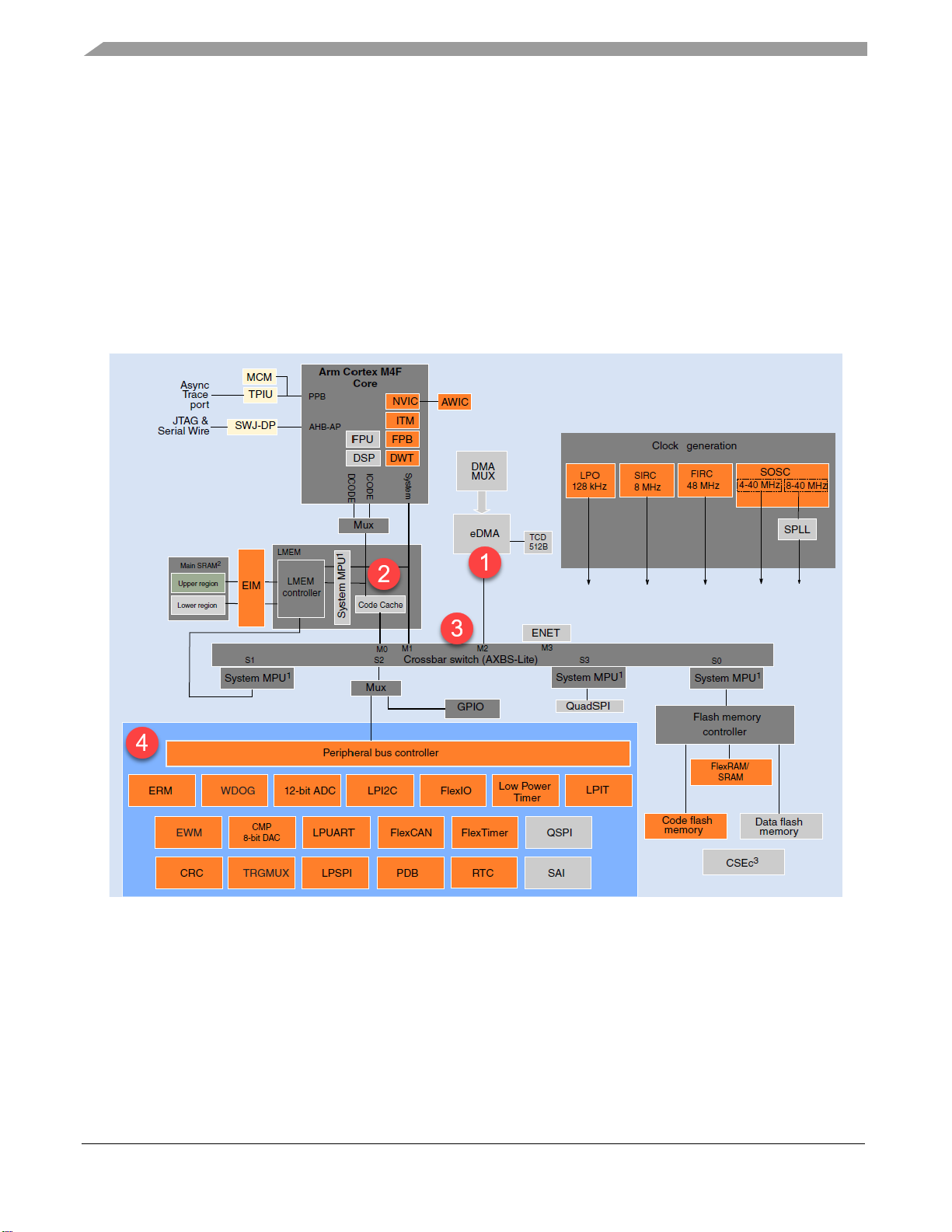
2. Integration of the eDMA module on S32K14x
The following figure shows the S32K14x product integration and it is followed by a list that shows some
features/components that may affect the performance of the data transfers.
Figure 1. S32K14x Block Diagram
1. eDMA options: Number of channels, priority configuration, bandwidth control, transfer size,
features enabled, etc. They will be discussed in next section.
2. Code cache: The chip includes one 4KB code cache to minimize the performance impact of
memory access latencies. The LMEM controller provides the processor with tightly-coupled
processor-local memories and bus paths to all slave memory spaces.
3. Crossbar switch: AXBS provides arbitration among the bus masters when they access the same
slave. One bottleneck arises when one eDMA tries to access SRAM (or any slave bus) while
Page 3
Integration of the eDMA module on S32K14x
Optimizing the S32K1xx eDMA for Performance Demanding Applications, Rev. 0, 02/2021
NXP Semiconductors 3
other master bus (i.e. CPU) tries to access that slave bus as well. Depending on the application
use case, it could be needed to add bandwidth control with MCM_CPCR[CBRR] register.
MCM_CPCR[CBRR] could program the crossbar arbitration as round robin or fixed priority.
Applications that require the eDMA to have control of the bus as much as possible, they will
need to set fixed priority (with starvation risk of other masters).
4. Peripheral configuration: depending in the application that it is needed to implement, it could be
some configuration of the peripheral related with eDMA that can improve the performance. In
next chapter it will be discussed some use cases.
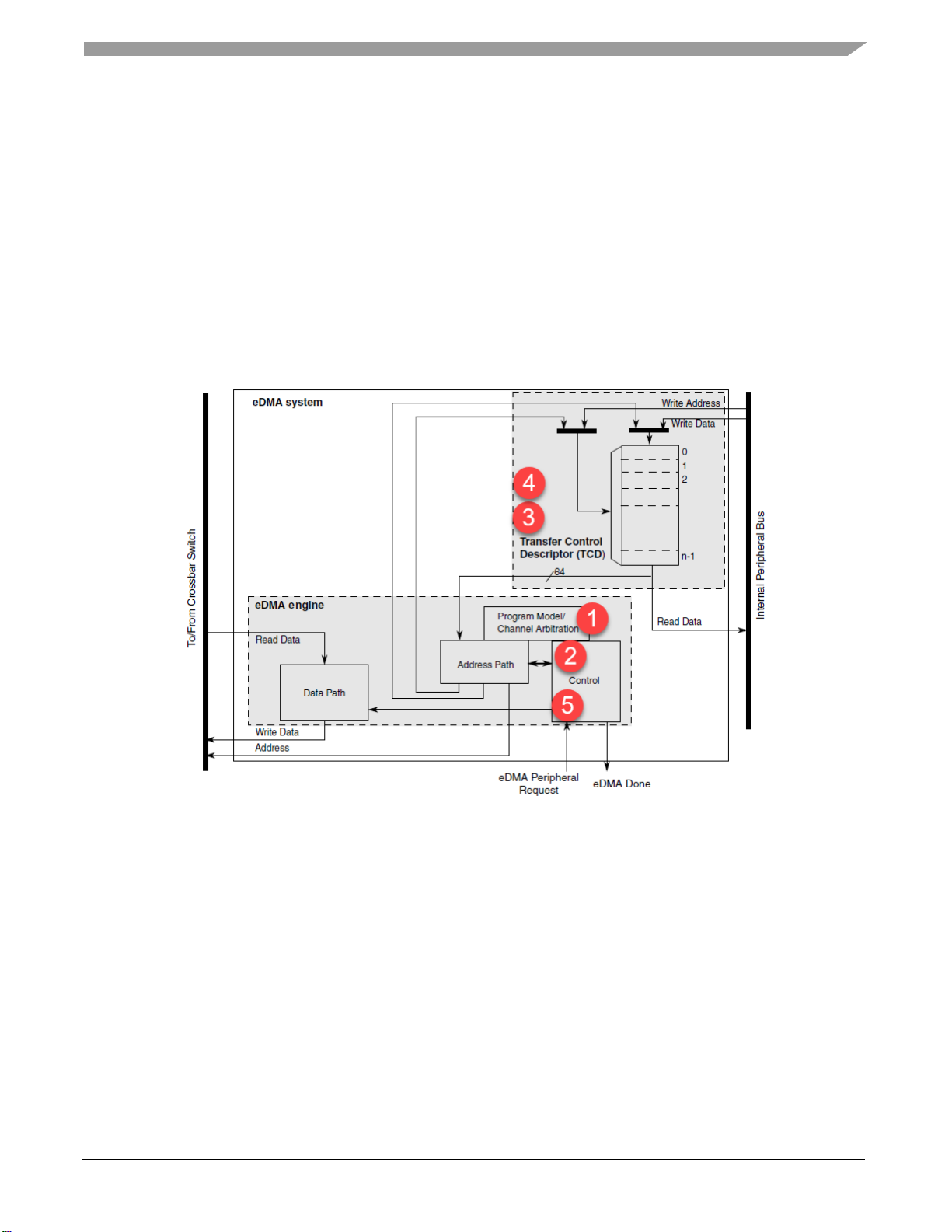
The following figure shows the eDMA internal composition, followed by a list of configurations which
might impact eDMA performance.
Figure 2. eDMA Block Diagram
Page 4

Integration of the eDMA module on S32K14x
Optimizing the S32K1xx eDMA for Performance Demanding Applications, Rev. 0, 02/2021
4 NXP Semiconductors
1. Priority configuration: eDMA has the capability to select fixed priority or round robin between
channels, depending on the application, you could need one channel to have higher priority than
others. It is more optimum to have fixed priority and assigned higher priority to critical channels,
but some cases and depending in the application, this is not an option.
2. Number of channels: As long as there is only one eDMA engine, only one channel can be
serviced at a time. With more active channels and constant eDMA requests, it is very likely to
have delays to attend one channel as other channel is being attended.
3. Bandwidth control: In some applications (with large transfer size) you need to avoid starvations
of other bus master in the crossbar, and in order to do this, eDMA can stall its own engine for
each R/W operation. This option allows other masters (like CPU) to take control of the slave port
and be able to work along with the eDMA. This feature does not improve the performance, but it
needs to be taken in consideration for some implementations.
4. Transfer size: eDMA supports programmable source, destination and transfer size, for data
transfers where the source and destination sizes are equal, the eDMA engine performs a series of
source-read / destination-write operations. For descriptors where the sizes are not equal, multiple
accesses of the smaller size data are required for each reference of the larger size. E.g. Source
sizes references 8-bit data and destination is 32-bit data, four reads are performed, then one
single 32-bit write.
5. eDMA Features enabled: There are some features of the eDMA (like Scatter gather, linking
channel or Minor loop offset) that can ease the implementation of specific applications. Some of
those features has the disadvantage of increasing transfer times and in those cases, software
designer must analyze the potential benefits at the expense of eDMA performance.
2.1.
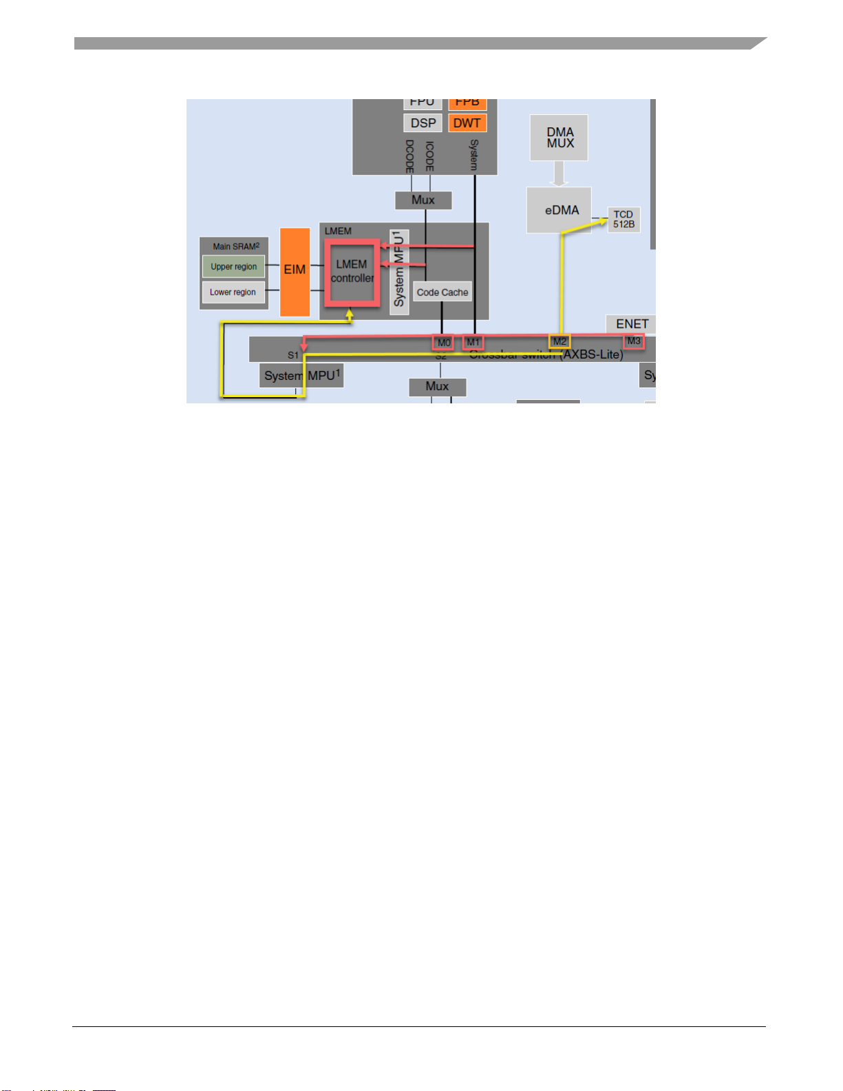
Scatter Gather feature
Scatter Gather (SGA) feature allows an eDMA channel to load different Transfer Control Descriptors
(TCD) when major loop is completed. The basic idea is that when one channel completes its major loop,
the channel will be reloaded with a new TCD that is saved in local memory, all without the intervention
of the CPU.
This capability allows the user to define different TCDs for one channel, but it causes a delay in the
eDMA transfers because to load the new TCD at the end of the major loop the eDMA engine needs to
de-reference the pointer address of the TCD from the memory where it was saved (flash or RAM), so
the eDMA engine needs to go through some busses to reach it, this represents clock cycles added to the
process which could increase depending in bus availability.
The following figure shows the path that the eDMA engine must go through in order to recharge the
TCD config (yellow) and the possible bottleneck by bus traffic (red) (assuming TCD is saved in RAM).
Page 5
Integration of the eDMA module on S32K14x
Optimizing the S32K1xx eDMA for Performance Demanding Applications, Rev. 0, 02/2021
NXP Semiconductors 5
Figure 3. eDMA path to RAM memory when TCD reloading
2.2.
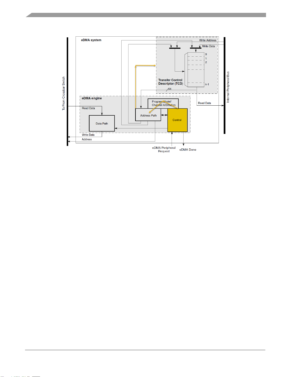
Channel to channel linking
Linking channel feature allows to trigger a eDMA channel when another eDMA channel completes a
transfer (major or minor loop). This capability allows to “connect” or “link” channels, so when one
transfer is completed, other transfer config from another channel can start. This feature is often used
when one transfers depends on the job of another transfer or when a specific order of transfers is
required.
This feature is a better option than the scatter gathers in terms of memory and time. Contrary to SGA,
linking channel does not use extra memory space (for the TCD configs) as you configure the channel
directly in the registers of the eDMA channel. Now, as the eDMA engine does not have to go through
any external bus (like the crossbar bus) to reload the TCD, linking channel does not add time to the
process (only the normal startup time for the eDMA channel).
This feature is limited to the number of channels available, which represent a limit number of TCD
configurations. Also, the minor link feature shares the register space memory with the NBYTES field,
therefore if you enable minor linking channel feature, you will be limited to 512 transfers or minor loops
count.
In the following figure you can see how the control submodule perform the linking process without
going out to crossbar bus and internal bus.
Page 6
Integration of the eDMA module on S32K14x
Optimizing the S32K1xx eDMA for Performance Demanding Applications, Rev. 0, 02/2021
6 NXP Semiconductors
Figure 4. Linking process inside eDMA module
Page 7

Use cases
Optimizing the S32K1xx eDMA for Performance Demanding Applications, Rev. 0, 02/2021
NXP Semiconductors 7
2.3.
eDMA data transfer process
The flow of any eDMA data transfer can be partitioned into three segments.
Table 1. eDMA transfer process
Channel
Activation
eDMA request (peripheral or software) is registered internally and then routed
through the eDMA engine.
Channel arbitration is performed (fixed-priority or round-robin).
The activated channel number is converted into the required address to access.
TCD memory is accessed, the required descriptor is read from the local memory
and loaded into the eDMA engine.
Read / Write
The source reads are initiated, and the fetched data is temporarily stored in the
data path block. Data will be there until it is gated onto the internal bus during the
destination write.
This process continues until the minor byte count has transferred.
TCD Reloading
Address path logic performs the required updates to certain fields in the
appropriate TCD.
If the major iteration count is exhausted, additional operations are performed such
as final address adjustments and BITER reloading.
Assertion of an optional IRQ or possible fetch of a new TCD from memory
(using scatter/gather) also occur at this time.
The table below summarizes the previous process and shows the theorical transfer time, assuming the
crossbar bus is free. Please, note that these numbers represent an ideal scenario.
Table 2. eDMA ideal transfer timing
Channel Active
7 cycles for
start-up.
Transfer
3 cycles for read
4 cycles for write
eDMA scatter/gather
intervention
11 cycles
3. Use cases
As mentioned at the beginning of this application note, the transfer time and performance vary according
to the application, this chapter proposes some use-cases to highlight the points we have reviewed so far.
Page 8
Use cases
Optimizing the S32K1xx eDMA for Performance Demanding Applications, Rev. 0, 02/2021
8 NXP Semiconductors
3.1.
eDMA for serial communications
3.1.1.
LPUART and FLEXIO
Consider a scenario where we enable two serial communication, one instance with LPUART and
another one with FlexIO emulating UART, both in full duplex mode. MCU will run the core at 80 MHz
and bus at 40 MHz and for this implementation the baud rate is at 10 Mbps in both communications.
In order to increase the performance of the MCU, we will include eDMA and this will allow us to avoid
reading and writing data into peripheral buffer with the CPU. Normally you would consider two eDMA
descriptors for each serial communication, which are one for TX (internal RAM to transmission buffer)
and one for RX (reception buffer to internal RAM). But for this use case, we will consider a scenario
where we want to modify the addresses of the internal Rx or Tx data.
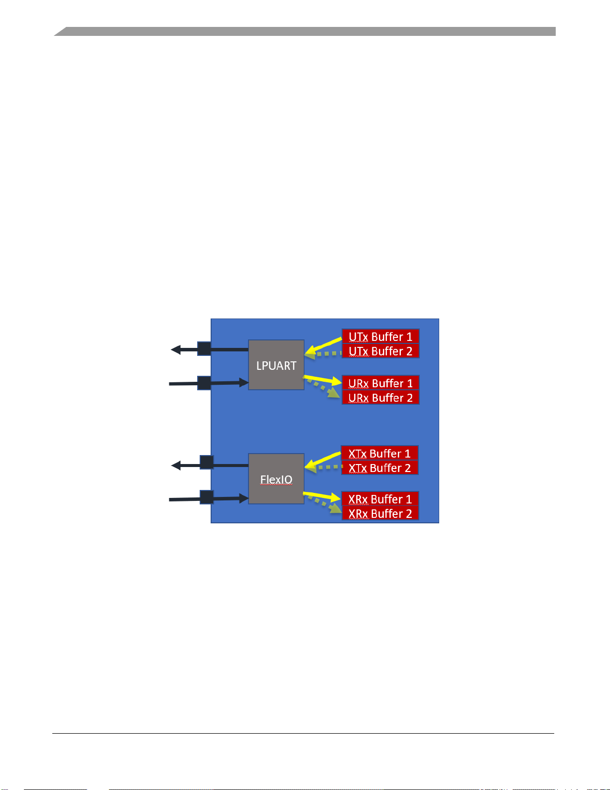
As you can see in the following image, red squares represent the internal RAM buffers, and the yellow
arrows the four transfers that eDMA will perform. eDMA module can take the data from/to buffer 1 or
buffer 2.
Figure 5. LPUART and FlexIO communication
In order to implement this, we need to use four eDMA channels (two for tx and two for Rx), and with
scatter gather, we enable the ability to change the RAM buffers locations.
There are three important points to consider here which will impact this implementation; number of
channels, baud rate and scatter gather enabling.
As we need two full-duplex communication we will use four channels, this represents a great workload
to the eDMA, because with 10 Mbps we have 1 MBps (8 data bits + start bit + stop bit = 10 bits per
UART transfer), which gives us a time slot request of 1uS. Time slot request is the interval of time
between two requests for the same channel
Page 9

Use cases
Optimizing the S32K1xx eDMA for Performance Demanding Applications, Rev. 0, 02/2021
NXP Semiconductors 9
This means that in order to avoid delays in Tx line (underrun) or possible missing info in Rx line
(overrun), eDMA should be able to receive four eDMA requests, handle them, and transfer the data in
less than 1µS (before another request from the same channel arrives).
Added to this, we also need to consider that scatter gather feature will introduce delay in the eDMA
process when the TCD is reloaded, giving us dependency in the RAM bus availability. The goal here is
optimize eDMA transfers to give enough time for the four eDMA channels.
Figure 6. Time slot request
Normally, delays in the Tx line are not serious issues in serial communication (they can be associated to
a timeout as error detection for example), but missing data in the Rx line in the other hand is a critical
issue that must be avoided. One option that we have in the LPUART module for S32K1 is the FIFO
buffer in Rx, enable it will increase the space to store received data in case Rx buffer hasn’t been read,
minimizing the risk of overruns and data losses. As the eDMA requests are triggered by the Watermark
value, we can leave this value as 0 and still the eDMA request will be triggered until the Rx FIFO buffer
is empty.
Results
Next scope shows the resulting transfer of this implementation. You will connect Uart Tx to Rx and
FlexIO Tx to Rx.
UART Tx eDMA channel perform four transfers from “UTx buffer 1” and then it reloads the TCD with
SGA feature. After this, eDMA pull data from “UTx buffer 2” and then it transfers another eight data.
UART Rx eDMA channel perform four transfers from UART buffer to “URx buffer 1” and then it also
reloads the TCD. It then saves other eight data received in “URx buffer 2”.
FlexIO Tx eDMA channel perform four transfer from “XTx buffer 1” and then it reloads the TCD with
SGA feature. After this, eDMA points to “XTx buffer 2” and then it transfers another eight data.
As we can observe the intervention of Scatter gather reloading is noted with delays in the UART output,
but inspecting the internal buffer “URx buffer 1” we saw that there is no data lost. For the case of
FlexIO we observe that there is not delays nor data lost.
Page 10

Use cases
Optimizing the S32K1xx eDMA for Performance Demanding Applications, Rev. 0, 02/2021
10 NXP Semiconductors
Figure 7. UART and FlexIO communication with Scatter gatter feature.
3.1.2.
SAI
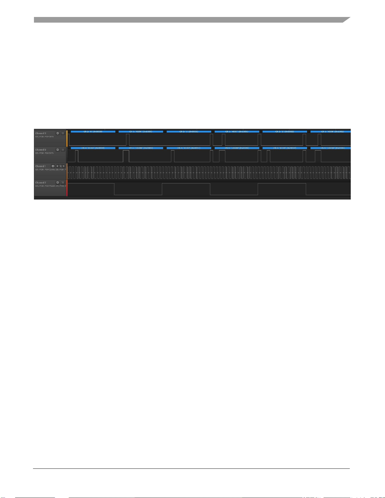
This document presents a use case of two Tx channels of 16-bit in I2S mode at 16 KHz. For other
eDMA usage in SAI module (ping pong buffer, separated channel, etc), refer to AN12202.
I2S (or TDM or any other audio protocol communication) is a special case of synchronous
communication where you can have different formats in the data array.
In a classic Tx I2S communication you have two data words in one line for each frame (Left and Right),
and in some cases the audio data should be processed in each channel separately, for these scenarios,
application code has separated “left” and “right” buffers and the eDMA is used to transfer the data from
different addresses (left and right buffers) to one buffer address (internal SAI tx buffer). In order to do
this, TCD can be configured to have an offset on each transfer.
Now, this case presents four data words in two lines for each frame (Ch0 L, Ch0 R, Ch1 L and Ch1 R),
and normally user could use two eDMA channels for each Audio channel, but eDMA channels would
need to be linked in the minor loop transfer, which as we already commented, it reduce the number of
transfer that can be set on TCD config. S32K148 SAI module has the “combining” feature, this feature
allows to “multiplex” SAI channels, so basically each write in the SAI channel 0 buffer is distributed in
all the enabled channels.
In the following figure you can see how combining the mode of SAI module and the minor loop offset
of the eDMA module works in conjunction for two channels left right config with separated buffers.
Figure 8. Combining mode in SAI module
This implementation will give the advantage of reducing eDMA resources to use only one eDMA
channel, also, it will not add time for scatter gather and we will not be forced to reduced data length for
linking channel.
Page 11
Use cases
Optimizing the S32K1xx eDMA for Performance Demanding Applications, Rev. 0, 02/2021
NXP Semiconductors 11
We don’t address the sample frequency topic, but in SAI module note that although there is no specific
minimum bus clock frequency specification, the bus clock must be fast enough (relative to the bit clock)
to ensure that the FIFOs can be serviced, without generating either a transmitter FIFO underrun or
receiver FIFO overflow condition.
Results
Next scope shows this implementation working normally, as you can see, 0x000x represent channel 0 L
data, 0x100x is channel 0 R, 0x200x channel 1 L and 0x300x channel 1 R. All of them in one frame (one
frame cycle).
Figure 9. Two Tx SAI channels with eDMA
3.2.
ADC readings through eDMA
As we know, ADC readings can be done through the eDMA, avoiding CPU intervention in the ADC_R
register and clear flags. Normal disadvantage of this is that you have a fix ADC channel, and to change
it you need to use the CPU.
There are some modules that are specialized in automating all the ADC process, including the ADC
channel change (like the BCTU in other Automotive devices), but we can emulate this capability with
some features of the eDMA. Flexible scan mode allows to perform the ADC conversion, save the value
in an internal buffer and change the ADC channel automatically, all with two eDMA channels and one
ADC converter.
Basic process can be divided in three parts;
1. The conversion complete flag COCO requests a eDMA transfer for eDMA channel 1.
2. The eDMA channel 1 transfer the ADC resulting value to the SRAM buffer.
3. Channel 1 is linked to eDMA channel 0, Channel 0 transfer from a RAM mux array to the
ADCx_SC (selector channel) a new ADC channel. Repeat step 1.
Page 12

Use cases
Optimizing the S32K1xx eDMA for Performance Demanding Applications, Rev. 0, 02/2021
12 NXP Semiconductors
Figure 10. Two Tx SAI channels with eDMA
All this process controlled by a timer that trigger ADC conversion (with a periodic triggering). These
steps can be repeated as many times as you need and you can have as many ADC ch saved as you need,
so this will mark the number of times that the ADC will convert and the number of transfers that the
eDMA will perform.
For example, if you have three ADC channels, and you need four measures for each channel, you will
have internal SRAM result buffer 3x4=12 values saved. Now if the ADC is triggered with a PDB timer
of 0.5 s, this process is going to take 0.5x12= 6s.
One important factor here is that the timer that trigger the conversion also sets the time slot request, this
mean that for our example ADC conversion, two eDMA transfers must happen in 500 ms. ADC SAR is
created with no intention of use it with fast conversions, but users must assure that there is enough time
for ADC conversions and two eDMA transfers (and any other possible time added by using eDMA in
other application).
Results
The following table shows an example of this implementation, with three ADC channels (Potentiometer,
VREFH and VREFL) and four measurements saved in internal SRAM memory.
Page 13

Use cases
Optimizing the S32K1xx eDMA for Performance Demanding Applications, Rev. 0, 02/2021
NXP Semiconductors 13
3.3.
Other factors
It’s time to evaluate some factors that could also affect the eDMA performance at SoC level.
Let’s assume a case where a huge amount of data has to be moved from Flash to the upper SRAM
region to then process it piece by piece, a [320x240] pixels image can be stored in an array of
76,800 bytes (in a real scenario, this data could be obtained by the user code through an acquisition
procedure from sensors e.g. cameras, or transmitted from other devices).
In order to obtain measurements of the time it takes the eDMA to do these operations, you will transfer
the whole array to a single SRAM-U location in a single request operation, transfer will be initiated by
software and the corresponding channel interrupt will be enabled.
The MCU will be in VLPR mode from 8 MHz SIRC, core and bus clocks will be set at 1 MHz and flash
clock will be 0.25 MHz. after initiating the eDMA transfer, CPU will enter an infinite loop with no
operations at all.
3.3.1.
CACHE
A cache is a block of high-speed memory locations containing address information (tag) and the
associated data. Its purpose is to decrease the average time of a memory access.
In this case, we are interested in the first principle of locality with which our cache operates, Spatial
locality: “An access to one location is likely to be followed by accesses from adjacent locations”.
Figure 11. Moving data from FLASH to Upper SRAM
The spatial locality property groups several locations together under the same tag. When data is loaded
into the cache, access times for subsequent loads are reduced, resulting in overall performance benefits.
Page 14

Use cases
Optimizing the S32K1xx eDMA for Performance Demanding Applications, Rev. 0, 02/2021
14 NXP Semiconductors
3.3.2.
Speculative Flash reads
The Flash controller (FMC) has a single buffer that reads ahead to the next word in flash memory.
When speculative reads are enabled, the Flash controller immediately requests the next sequential
address after a read is completed, this helps to reduce or even eliminate wait states when accessing
sequential code and/or data.
NOTE
Flash acceleration features are enabled by default.
Results
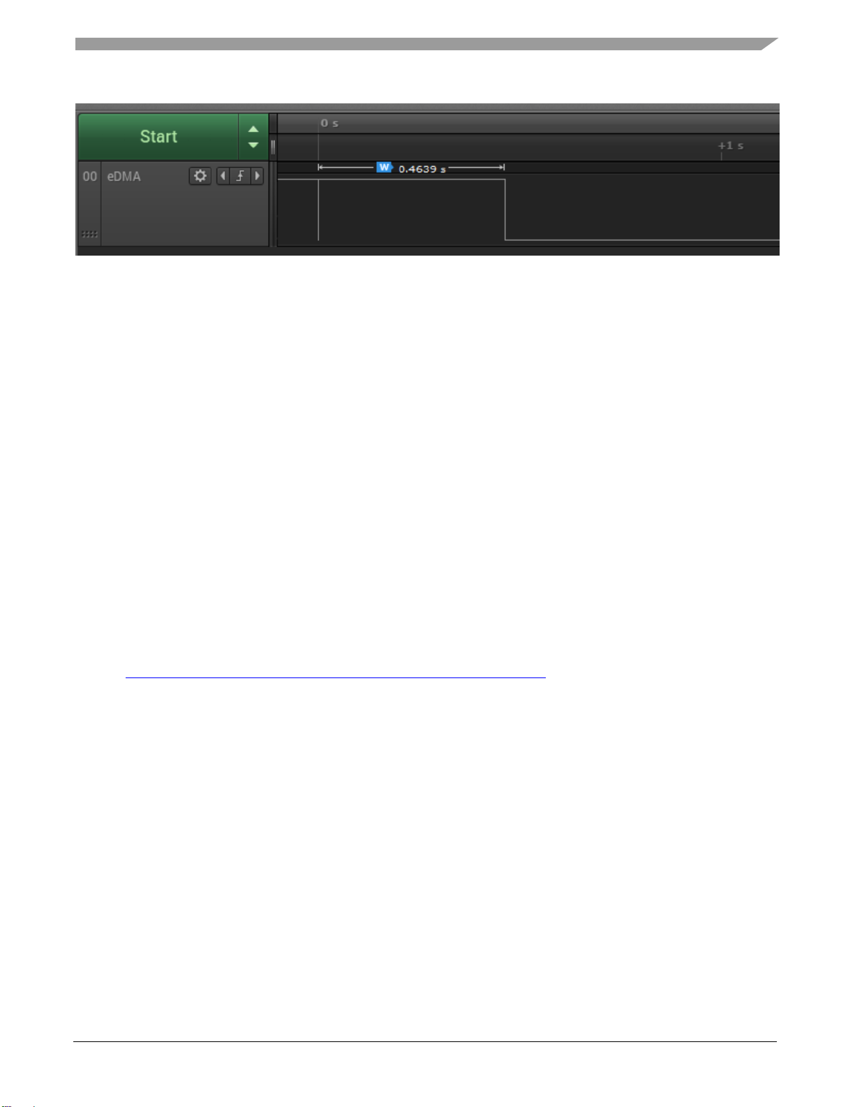
After reset, Cache is disabled, while Data prefetch and Flash speculate options are enabled. Let’s disable
Data Flash prefetch (MSCM_OCMDR[OCM1]) to see how long it takes.
Figure 12. eDMA Transfers 76,800 bytes
That took 0.9275 seconds, let’s enable the speculation for data (default settings from reset).
Figure 13. eDMA Transfers 76,800 bytes, Data Flash prefetch enabled
The transfer time decreased by 16.66 %, but we also have to review the role that Cache plays in this
case, to do that we will enable it with the LMEM controller.
Page 15
Reference
Optimizing the S32K1xx eDMA for Performance Demanding Applications, Rev. 0, 02/2021
NXP Semiconductors 15
Figure 14. eDMA Transfers 76,800 bytes, Cache enabled
You can see that it decreased to 0.4639 secs. (half the original time).
4. Conclusions
• The transfer data structure to TCD in Scatter-Gather mode causes small delay in data transfer.
• There are some features included in the eDMA module that could improve data transfer.
• There are some screws outside the eDMA block that we can tighten to improve the performance
of certain applications.
• Even if eDMA transfers takes a few clock cycles, whole time application could be affected by
bus traffic and not eDMA related problems.
• User should consider worst case scenario points and try to manage them with different features
and implementation.
5. Reference
• S32K1xx Data Sheet. 2020
• S32K14x Series Reference Manual. 2020
• https://www.nxp.com/docs/en/application-note/AN4590.pdf
Page 16

Reference
Optimizing the S32K1xx eDMA for Performance Demanding Applications, Rev. 0, 02/2021
16 NXP Semiconductors
Page 17

Page 18

Document Number: AN12972
Rev. 0
02/2021
How to Reach Us:
Home Page:
nxp.com
Web Support:
nxp.com/support
Information in this document is provided solely to enable system and software implementers
to use NXP products. There are no express or implied copyright licenses granted hereunder
todesign or fabricate any integrated circuits based on the information in this document. NXP
reserves the right to make changes without further notice to any products herein.
NXP makes no warranty, representation, or guarantee regarding the suitability of its products
for any particular purpose, nor does NXP assume any liability arising out of the application or
use of any product or circuit, and specifically disclaims any and all liability, including without
limitation consequential or incidental damages. “Typical” parameters that may be provided in
NXP data sheets and/or specifications can and do vary in different applications, and actual
performance may vary over time. All operating parameters, including “typicals,” must be
validated for each customer application by customer's technical experts. NXP does not convey
any license under its patent rights nor the rights of others. NXP sells products pursuant to
standard terms and conditions of sale, which can be found at the following address:
nxp.com/SalesTermsandConditions.
While NXP has implemented advanced security features, all products may be subject to
unidentified vulnerabilities. Customers are responsible for the design and operation of their
applications and products to reduce the effect of these vulnerabilities on customer’s
applications and products, and NXP accepts no liability for any vulnerability that is discovered.
Customers should implement appropriate design and operating safeguards to minimize the
risks associated with their applications and products.
NXP, the NXP logo, NXP SECURE CONNECTIONS FOR A SMARTER WORLD, OOLFLUX,
EMBRACE, GREENCHIP, HITAG, I2C BUS, ICODE, JCOP, LIFE VIBES, MIFARE, MIFARE
CLASSIC, MIFARE DESFire, MIFARE PLUS, MIFARE FLEX, MANTIS, MIFARE
LTRALIGHT, MIFARE4MOBILE, MIGLO, NTAG, ROADLINK, SMARTLX, SMARTMX,
TARPLUG, TOPFET, TRENCHMOS, UCODE, Freescale, the Freescale logo, AltiVec, C‑5,
CodeTEST, CodeWarrior, ColdFire, ColdFire+, C‑Ware, the Energy Efficient Solutions logo,
Kinetis, Layerscape, MagniV, mobileGT, PEG, PowerQUICC, Processor Expert, QorIQ, QorIQ
Qonverge, Ready Play, SafeAssure, the SafeAssure logo, StarCore, Symphony, VortiQa,
Vybrid, Airfast, BeeKit, BeeStack, CoreNet, Flexis, MXC, Platform in a Package, QUICC
Engine, SMARTMOS, Tower, TurboLink, and UMEMS are trademarks of NXP B.V. All other
product or service names are the property of their respective owners. AMBA, Arm, Arm7,
Arm7TDMI, Arm9, Arm11, Artisan, big.LITTLE, Cordio, CoreLink, CoreSight, Cortex,
DesignStart, DynamIQ, Jazelle, Keil, Mali, Mbed, Mbed Enabled, NEON, POP, RealView,
SecurCore, Socrates, Thumb, TrustZone, ULINK, ULINK2, ULINK-ME, ULINK-PLUS,
ULINKpro, μVision, Versatile are trademarks or registered trademarks of Arm Limited (or its
subsidiaries) in the US and/or elsewhere. The related technology may be protected by any or
all of patents, copyrights, designs and trade secrets. All rights reserved. Oracle and Java are
registered trademarks of Oracle and/or its affiliates. The Power Architecture and Power.org
word marks and the Power and Power.org logos and related marks are trademarks and
service marks licensed by Power.org.
© 2021 NXP B.V.
 Loading...