

Page 1

NXP Semiconductors Document identifier: QCVS_DDR_User_Guide
User's Guide Rev. 4.x, 01/2021
QCVS DDR Tool User Guide
Page 2

NXP Semiconductors
Contents
Chapter 1 DDR Configuration and Validation........................................................ 3
1.1 DDR configuration..................................................................................................................... 3
1.1.1 Using DDR configuration tool......................................................................................................3
1.1.1.1 Create a new QorIQ configuration project..................................................................................... 4
1.1.1.2 Configure DDR controller...............................................................................................................6
1.1.1.3 Generate code from DDR component......................................................................................... 11
1.1.2 Importing DDR configuration.....................................................................................................13
1.1.2.1 Memory dump formats................................................................................................................. 16
1.1.2.2 Get memory dump formats.......................................................................................................... 20
1.1.3 Exporting DDR configuration.....................................................................................................21
1.1.4 Advanced DDR configuration options....................................................................................... 21
1.1.4.1 DDR configuration by reading SPD............................................................................................. 22
1.1.4.2 DDR configuration by importing from target.................................................................................24
1.2 DDR validation.........................................................................................................................28
1.2.1 Overview of DDR validation UI..................................................................................................28
1.2.1.1 Validation scenarios panel........................................................................................................... 29
1.2.1.2 Validation control panel................................................................................................................30
1.2.1.3 Test configuration panel...............................................................................................................30
1.2.1.4 Scenario results panel................................................................................................................. 30
1.2.1.5 Validation page toolbar................................................................................................................ 32
1.2.2 Using DDR validation tool......................................................................................................... 33
1.2.2.1 Choose validation scenarios and tests........................................................................................ 33
1.2.2.2 Customize validation tests........................................................................................................... 34
1.2.2.3 Run validation.............................................................................................................................. 36
1.2.2.4 Report validation results.............................................................................................................. 37
1.2.2.5 Set DDR validation preferences...................................................................................................38
1.2.3 Advanced DDR validation operations....................................................................................... 39
1.2.3.1 DDR validation using margin scenarios....................................................................................... 39
1.2.3.2 DDR validation using stressing scenarios....................................................................................43
1.2.3.3 DDR validation with warm boot....................................................................................................45
1.2.3.4 Validation code customization..................................................................................................... 47
1.2.4 Licensing................................................................................................................................... 48
QCVS DDR Tool User Guide, Rev. 4.x, 01/2021
User's Guide 2 / 49
Page 3

NXP Semiconductors
Chapter 1
DDR Configuration and Validation
This document introduces the double data rate (DDR) RAM configuration and validation tool, which is an embedded component
of QorIQ Configuration and Validation Suite (QCVS).
The DDR tool has two components: DDR configuration tool and DDR validation tool. The DDR configuration tool allows you to
create a configuration for the DDR component and the DDR validation tool allows you to validate the DDR configuration using
various validation scenarios.
This chapter is divided into the following sections:
• DDR configuration
• DDR validation
1.1 DDR configuration
This section describes how to create a new QorIQ configuration project, how to configure the DDR component, and how to
perform some basic operations using the DDR configuration tool.
The DDR configuration tool inside the QCVS configures the DDR controller embedded in various supported QorIQ/Qonverge
device families.
The DDR configuration tool provides a user-friendly graphical interface to configure the DDR controller. It can be used for tweaking
some of the configuration parameters when you want to use different DDR Dual In-line Memory Modules (DIMMs) than the ones
received with the board or when you want to optimize the DDR configuration.
While configuring DDR, you can view register values of the DDR controller. The register values will be exported by the DDR
tool into C, TCL, or GDB code. After configuring the DDR controller, you can generate code that will fit easily into your software
environment in the following ways:
• OS-agnostic low-level C source code that configures the DDR controller(s) registers' values.
• C source code that outputs the register values in the format required by U-Boot. This file can replace an existing file inside
uBoot.
• Source code in DDR related part of the CodeWarrior target initialization file *.tcl. The code in this file can be used inside
CodeWarrior projects.
This section contains the following subsections:
• Using DDR configuration tool
• Importing DDR configuration
• Exporting DDR configuration
1.1.1 Using DDR configuration tool
The DDR configuration tool helps you configure the DDR controller in a QorIQ processor, based on the DDR implementation
(discrete or DIMM) used in the processor.
The DDR implementation may differ by various parameters, such as number of chip selects, memory size, or ranks interleaving.
To configure a new DDR controller, you need to use the specifications from the DDR manufacturer data sheet and fill the values
in the interface. The DDR parameters are grouped together by functionality.
This section contains the following subsections:
• Create a new QorIQ configuration project
• Configure DDR controller
• Generate code from DDR component
QCVS DDR Tool User Guide, Rev. 4.x, 01/2021
User's Guide 3 / 49
Page 4
NXP Semiconductors
DDR Configuration and Validation
1.1.1.1 Create a new QorIQ configuration project
To use the DDR configuration tool, you first need to create a QorIQ configuration project with DDR configuration.
To create a new QorIQ configuration project for DDR configuration, follow these steps:
1. Select File > New > QorIQ Configuration Project. Follow the steps in the New QorIQ Configuration Project wizard.
2. Enter project name.
3. Select the target SoC.
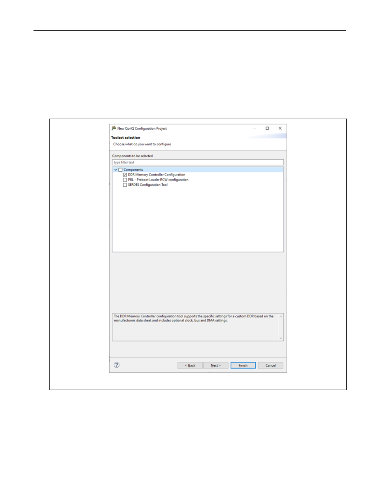
4. On the Toolset selection page, select the DDR Memory Controller Configuration checkbox.
Figure 1. Toolset selection page
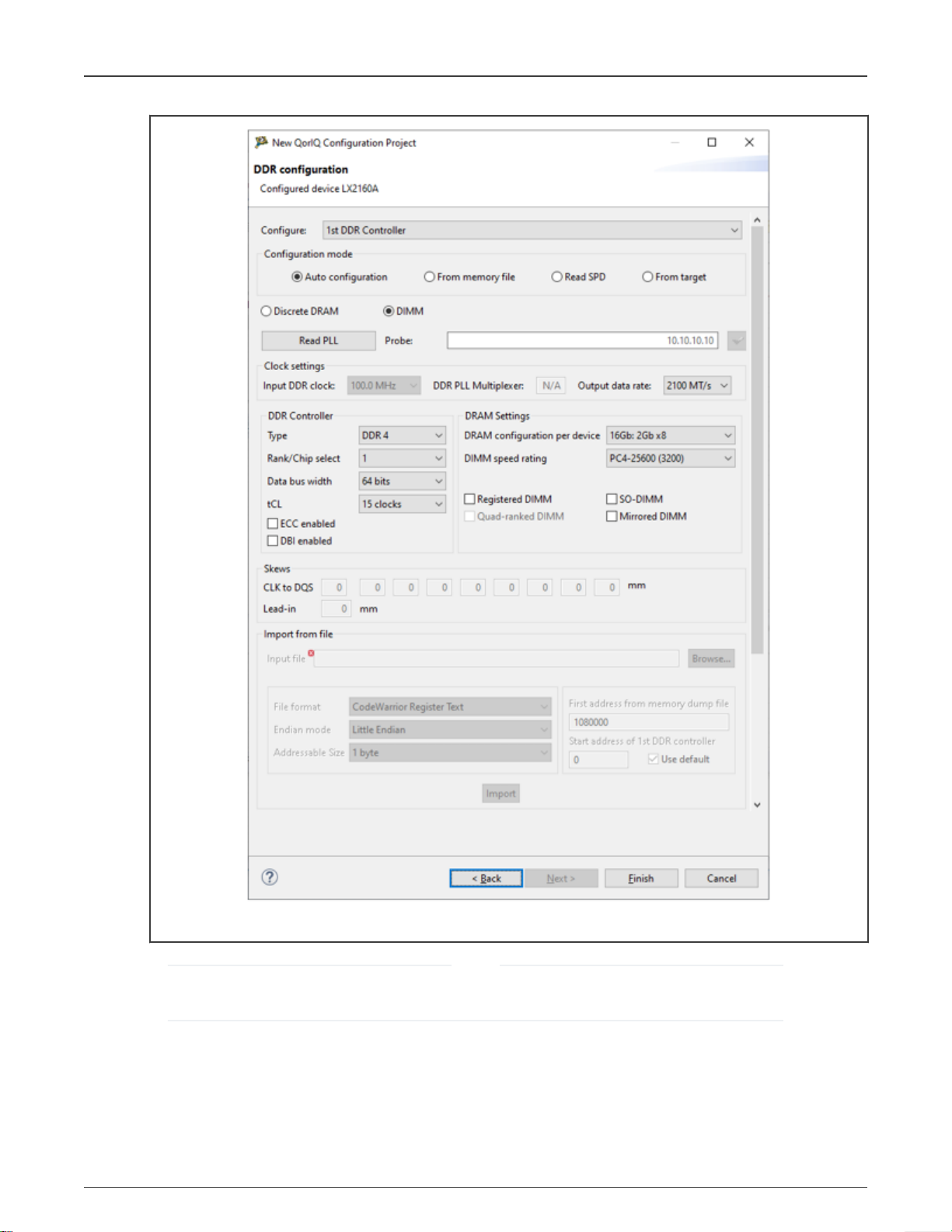
5. Click Next. The DDR configuration page appears.
• To configure the DDR with DIMM settings, select the DIMM option.
QCVS DDR Tool User Guide, Rev. 4.x, 01/2021
User's Guide 4 / 49
Page 5
NXP Semiconductors
DDR Configuration and Validation
Figure 2. DDR configuration for DIMM
NOTE
Lead-in skew is the difference between the A/C bus trace length and data bus trace length from the controller pins
to the DIMM connector pins.
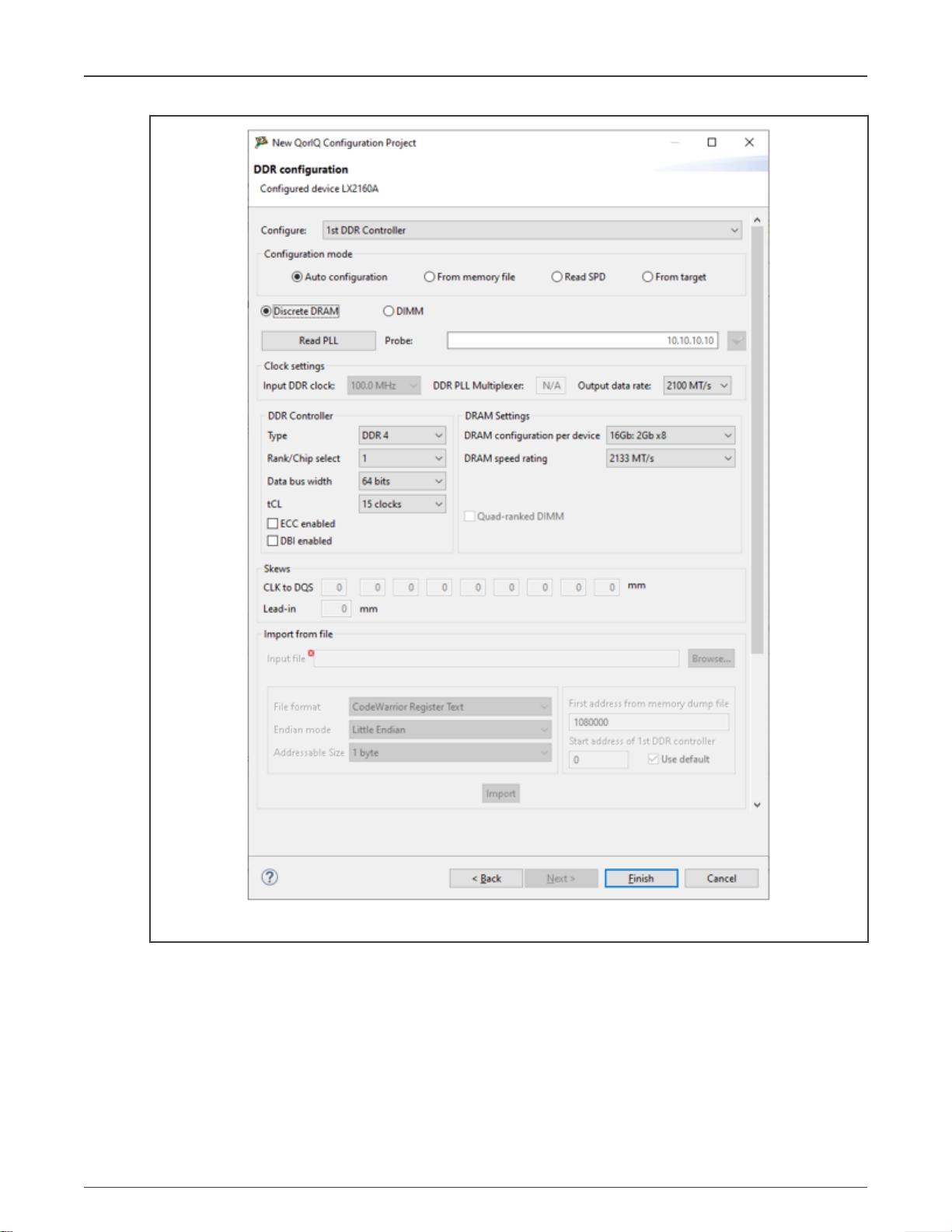
• For designs that utilize embedded, discrete devices, select the Discrete DRAM option.
QCVS DDR Tool User Guide, Rev. 4.x, 01/2021
User's Guide 5 / 49
Page 6
NXP Semiconductors
DDR Configuration and Validation
Figure 3. DDR configuration for discrete DRAM
6. Click Finish to complete project creation.
This creates a QorIQ configuration project for DDR configuration.
1.1.1.2 Configure DDR controller
After creating a QorIQ configuration project with the DDR toolset, you can configure the DDR controller using the DDR
configuration tool.
Perform the following steps to configure DDR controller:
QCVS DDR Tool User Guide, Rev. 4.x, 01/2021
User's Guide 6 / 49
Page 7
NXP Semiconductors
DDR Configuration and Validation
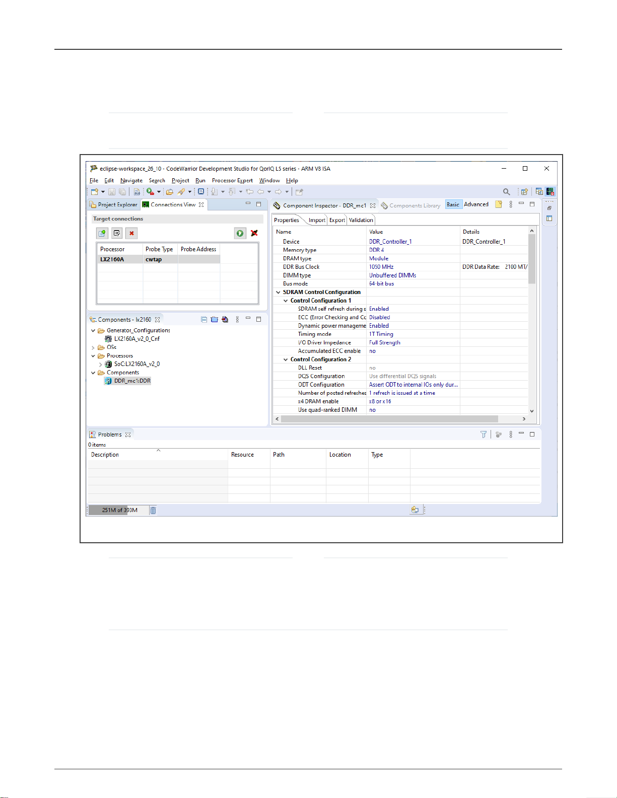
1. Select the DDR component under the Components folder in the Components view, as shown in the following figure. The
properties of the DDR component opens in the Component Inspector view.
NOTE
If the Component Inspector view is closed, you can open it by right-clicking the DDR component in the Components
view and choosing the Inspector option from the shortcut menu.
Figure 4. Select DDR components in Components view
NOTE
You can add multiple DDR components to a project. Each DDR component maps to one DDR controller of the SoC.
For example, LS2088A SoC has two embedded DDR controllers, so if you want to configure both of them, add two
DDR components from the Components Library to the project, one component for each controller. Right-click the
DDR component in the Categories tab and select Add to project with Wizard from the shortcut menu, as shown in
the following figure.
QCVS DDR Tool User Guide, Rev. 4.x, 01/2021
User's Guide 7 / 49
Page 8

NXP Semiconductors
Figure 5. Add DDR component to project
DDR Configuration and Validation
2. Modify the following basic DDR parameters according to your requirements:
• Memory type: Specify the DDR memory type, for example, DDR 4 or DDR 3L
Figure 6. Set memory type
• DDR Bus Clock: For each DDR bus clock, there is a specific bus clock frequency that measures the duration of a
bus clock cycle
Figure 7. Set DDR bus clock
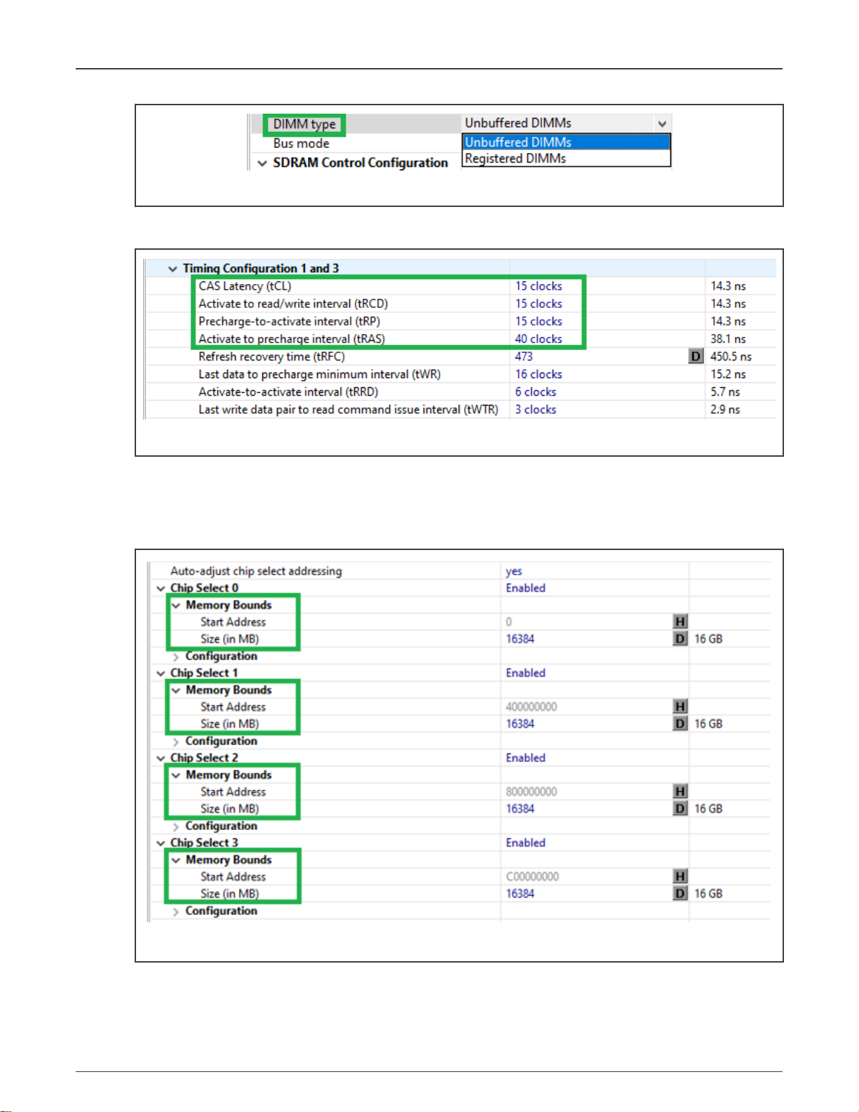
• DIMM type: Specify the DIMM type: unbuffered or registered
QCVS DDR Tool User Guide, Rev. 4.x, 01/2021
User's Guide 8 / 49
Page 9
NXP Semiconductors
Figure 8. Set DIMM type
DDR Configuration and Validation
• Timing Configuration 1: Set four basic DDR timings:
tRAS
. The timings are measured in bus clock cycles.
tCL, tRCD, tRP, tRAS
specified usually as
tCL-tRCD-tRP-
Figure 9. Set timing configuration 1
• Chip Select 0, 1, 2, 3: Specify the number of physical ranks or chip selects. A DIMM can have 1, 2, or 4 ranks and
are specified in the basic DIMM information as 1R ... or 2R... or 4R. For this, from the four chip selects, enable the
ones that correspond to the ranks (each chip select corresponds to one rank). Also, set size of the DIMM. The size
is configured inside each chip select. For example, a 32 GB dual-ranked DIMM has its size split evenly between the
two ranks such that each chip select is of 16 GB size.
Figure 10. Set chip select / physical ranks
3. Set rest of the parameters as per the datasheet of the DDR device. The datasheet can be obtained from the DDR
manufacturer's website or directly from the DDR manufacturer.
QCVS DDR Tool User Guide, Rev. 4.x, 01/2021
User's Guide 9 / 49
Page 10
NXP Semiconductors
DDR Configuration and Validation
NOTE
For each step of the configuration process, you might receive validation errors for some specific parameters along
with information on how to fix the validation conflict.
You can import register values of the DDR component from a memory dump, containing the values of the DDR memory-mapped
registers. Memory dumps can be obtained from U-Boot (using the md command) or CodeWarrior (using the Export registers/
memory feature).
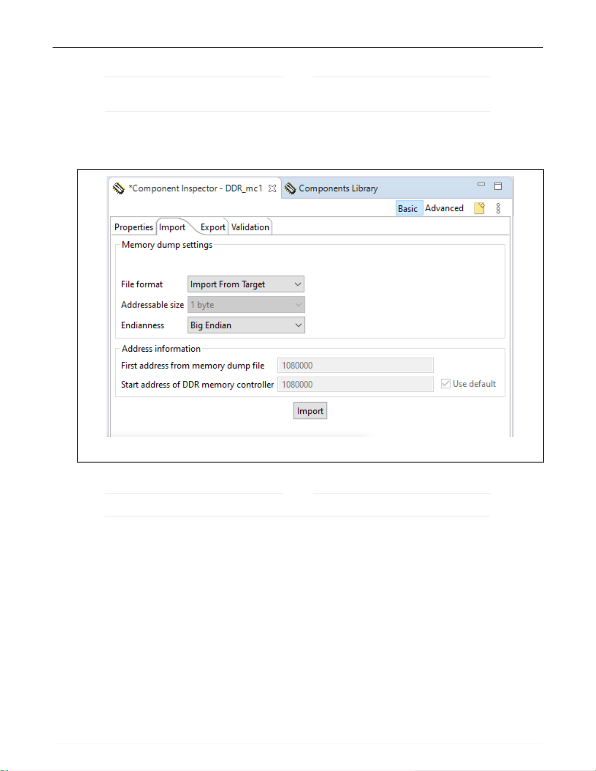
1. Select the Import tab in the Component Inspector view.
Figure 11. Import tab - DDR component
2. Specify the location of the input file in the Input file field. The red mark denoting an error/conflict disappears.
NOTE
The red marks indicate errors; therefore, before clicking the Import button, ensure that no red mark is displaying.
3. Choose an appropriate file format for the input file from the File format menu. If the file content is not in accordance with
the chosen format, the import operation will fail and an error message will pop up.
4. Specify the number of bytes by choosing an option from the Addressable size menu.
5. Specify byte order by choosing an option from the Endianness menu.
6. Specify valid address information of the memory dump file in the First address from memory dump file field.
7. Specify the beginning address of the memory-mapped DDR registers inside the memory dump in the Start address of
DDR memory controller field. The First address from memory dump file and Start address of DDR memory controller
fields are enabled for editing only after deselecting the Use default checkbox.
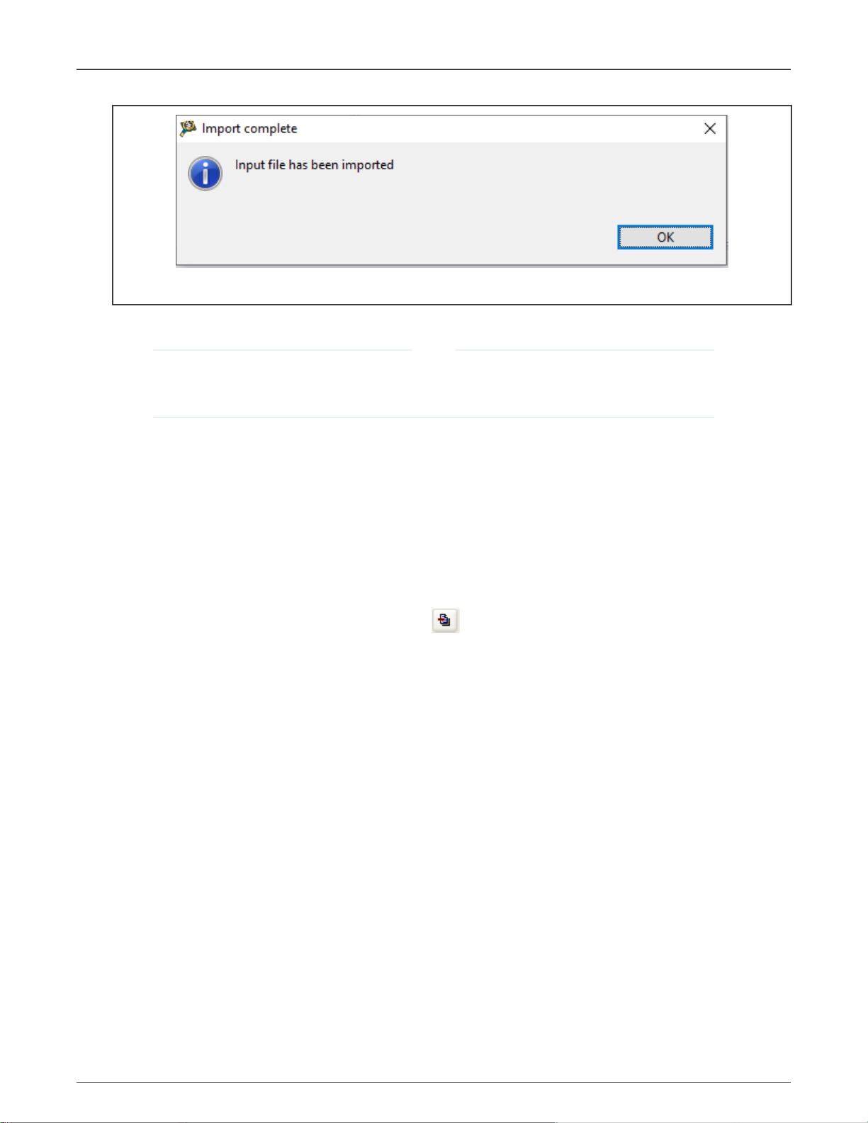
8. Click Import. The input file is imported.
9. Click OK in the Import complete dialog (shown below).
QCVS DDR Tool User Guide, Rev. 4.x, 01/2021
User's Guide 10 / 49
Page 11
NXP Semiconductors
Figure 12. Import complete dialog
10. Open the Problems view to see reported errors if any.
You can also configure the DDR component while creating the QorIQ project. On the DDR Configuration page (see
Figure 3), select the appropriate option, Auto configuration or From memory file, and provide the necessary details
corresponding to the selected option.
1.1.1.3 Generate code from DDR component
NOTE
DDR Configuration and Validation
After you finish configuring the DDR controller, you can generate code from DDR component to get updated output of the
component.
The source code generated from the DDR component helps you configure the DDR controller registers and it can be used in the
CodeWarrior projects.
The code generation from the DDR component is based on the properties set in the Component Inspector view. You can use any
of the following options to generate DDR component code:
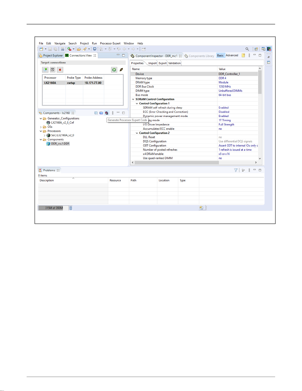
• Click the Generate Processor Expert Code icon
in the Components view, as shown in the following figure.
• Right-click ProcessorExpert.pe in the Project Explorer and choose Generate Processor Expert Code from the shortcut
menu.
• Choose the Project > Generate Processor Expert Code option from the Eclipse IDE menu.
QCVS DDR Tool User Guide, Rev. 4.x, 01/2021
User's Guide 11 / 49
Page 12
NXP Semiconductors
DDR Configuration and Validation
Figure 13. Generate Processor Expert code
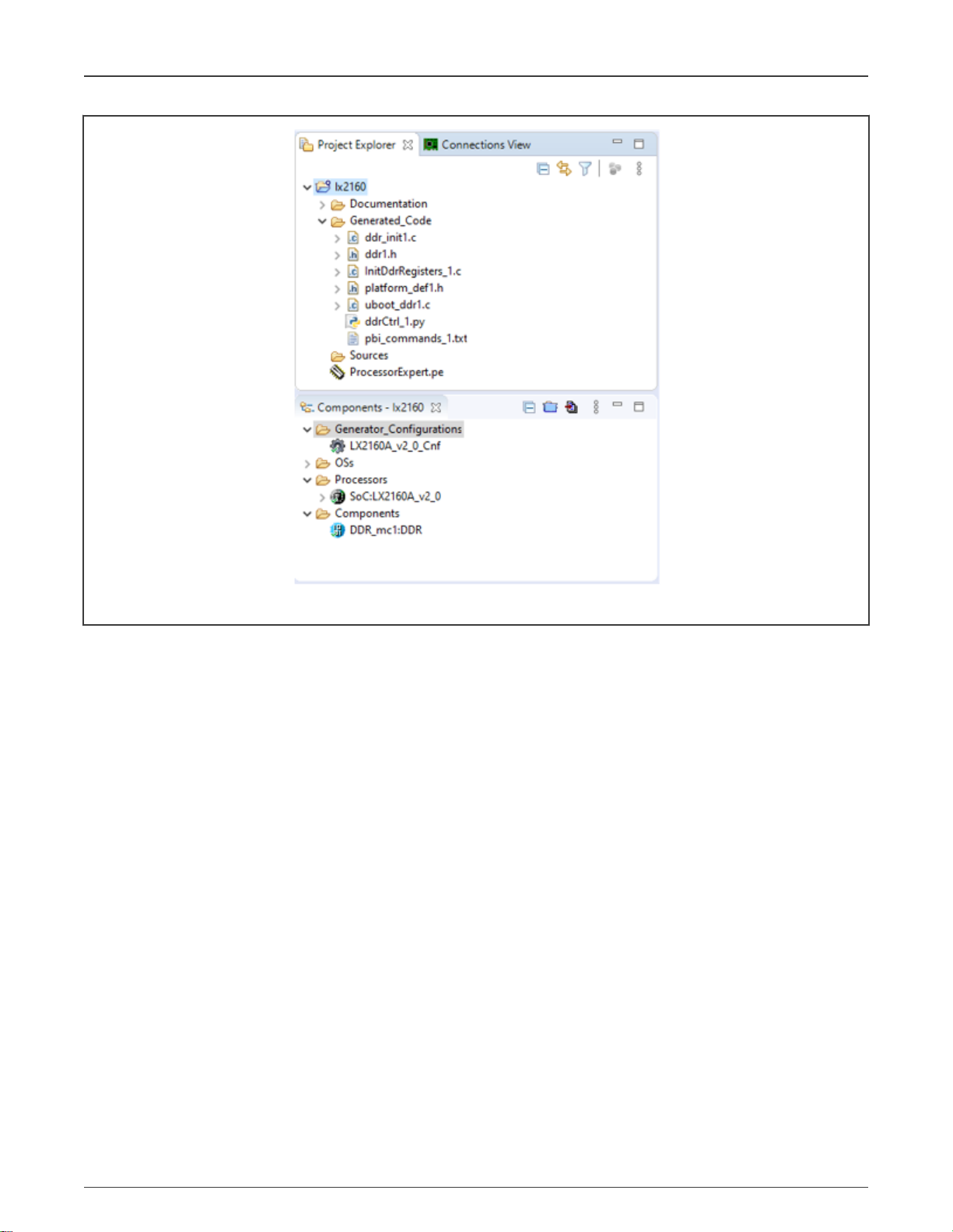
The output file is generated and placed in the Generated_Code folder of the Project Explorer. The output file is named according
to the DDR component name used in the QorIQ Configuration project, as shown in the figure below.
QCVS DDR Tool User Guide, Rev. 4.x, 01/2021
User's Guide 12 / 49
Page 13
NXP Semiconductors
DDR Configuration and Validation
Figure 14. DDR-generated code file in Project Explorer
1.1.2 Importing DDR configuration
The DDR tool allows you to import a memory dump, which can be in a format, such as U-Boot, S-Record, AnnotatedHex,
Signed/Unsigned decimal, CodeWarrior Regs, Hex, or Raw Binary.
The memory dump is decoded into a DDR configuration, which then can be visualized, validated, and adjusted, if required.
To import a DDR configuration, a QorIQ Configuration project must be created. You can import the DDR configuration during
project creation or later for any component already added to the project. Perform the following steps:
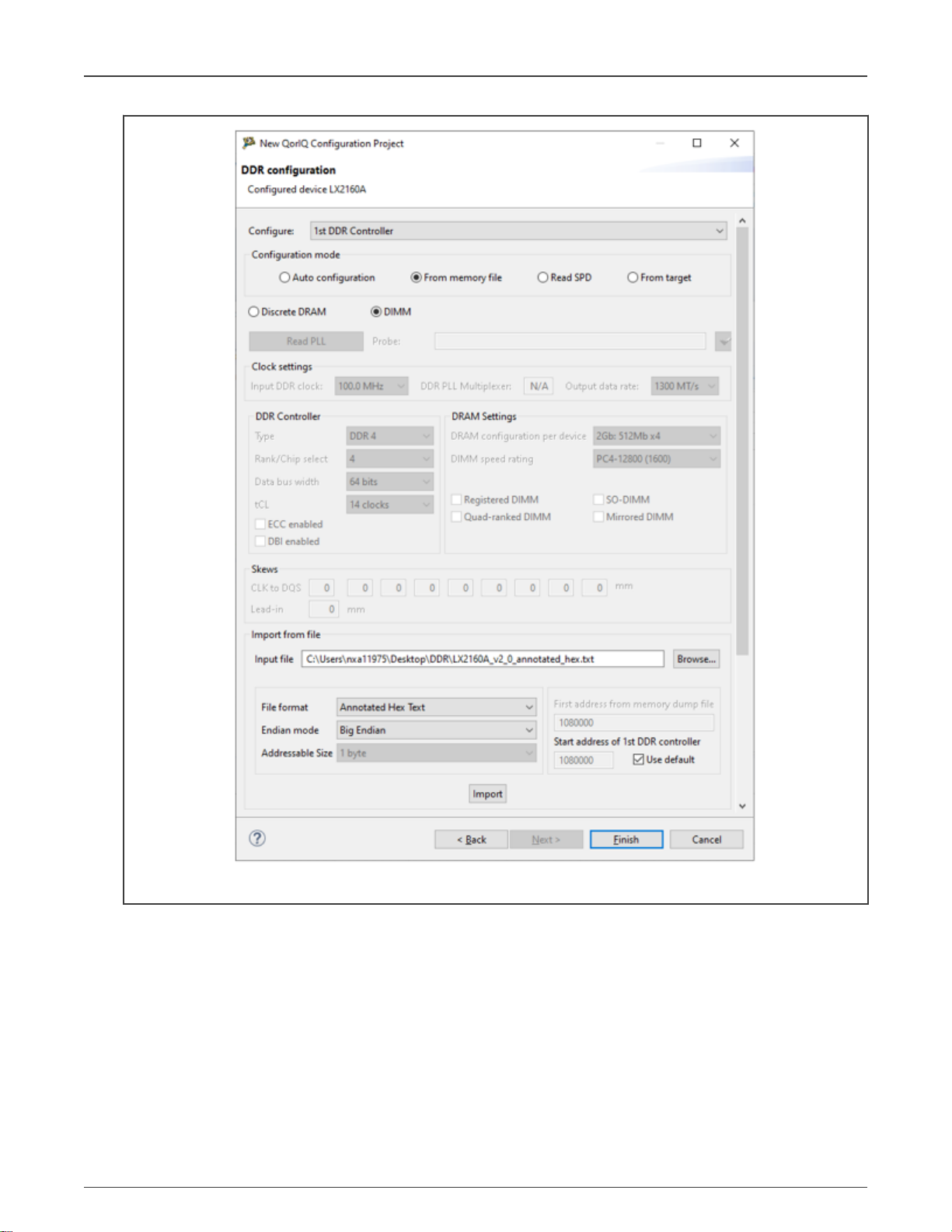
1. On the DDR Configuration page of the New QorIQ Configuration Project wizard (shown below), select the From memory
file option.
2. Specify the memory dump file to be imported in the Input file text box.
3. Based on file content, choose a file format for the input file from the File format menu.
4. Choose byte order from the Endian mode menu.
5. Click Import and wait to see if the import was done correctly. The Finish button will be enabled.
QCVS DDR Tool User Guide, Rev. 4.x, 01/2021
User's Guide 13 / 49
Page 14
NXP Semiconductors
DDR Configuration and Validation
Figure 15. Selecting input file for DDR configuration
6. Click Finish. The DDR project is created.
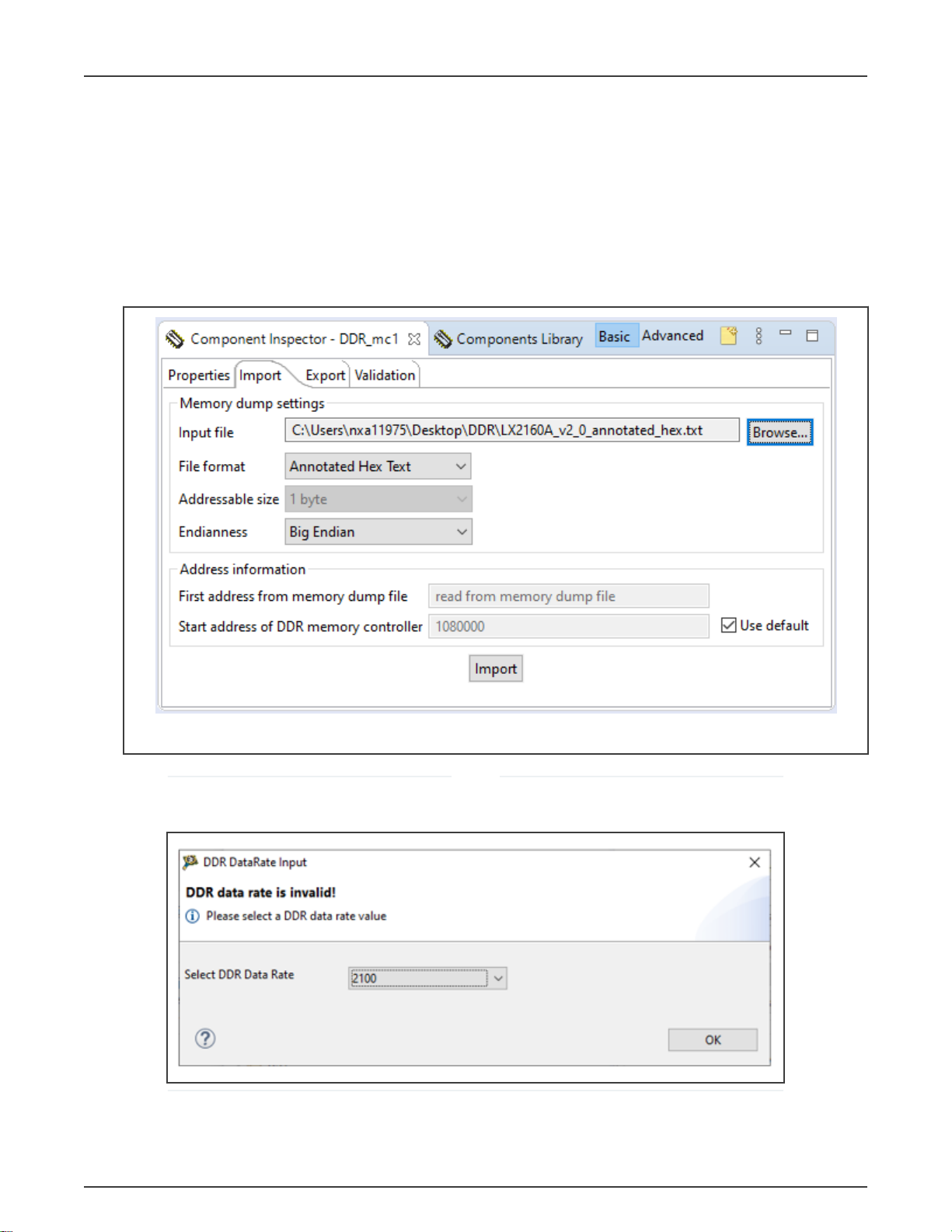
7. Open Component Inspector for the DDR project.
8. Select the Import tab and set the following parameters as shown in the next figure:
• Input file: Specify the file that encapsulates the memory dump
• File format: Choose a file format for the input file based on the file content. If the file content is not in accordance
with the chosen format, the import operation will fail and an error message will pop up.
You can also import a DDR configuration from the target board by choosing Import from target from the File format
menu. This action only works if an active and working connection is configured in the Connections View (see
Getting Started Guide
User's Guide 14 / 49
for more information). If such a connection exists, the DDR tool reads the DDR registers from
QCVS DDR Tool User Guide, Rev. 4.x, 01/2021
QCVS
Page 15
NXP Semiconductors
the board and populates the active component with the data read. Note that this type of action is relevant only if the
DDR registers were previously configured (for example, by U-Boot).
• Addressable size: Specify the number of bytes
• Endianness: Specify byte order
• First address from memory dump file: Specify valid address information of the memory dump file
• Start address of DDR memory controller: Specify the beginning address of the memory-mapped DDR registers
inside the memory dump. The First address from memory dump file and Start address of DDR memory controller
fields are enabled for editing only after deselecting the Use default checkbox.
DDR Configuration and Validation
Figure 16. Component Inspector - Specifying import parameters
NOTE
In case the input file does not contain the DDR data rate value on the first line, you will be prompted to choose a
data rate value.
This is how a DDR configuration can be imported.
QCVS DDR Tool User Guide, Rev. 4.x, 01/2021
User's Guide 15 / 49
Page 16

NXP Semiconductors
NOTE
While performing the import operation during project creation, you can configure all the DDR controllers. Choose
the current DDR controller from the Configure list on the DDR Configuration page (see Figure 15). If you import from
Component Inspector for DDR, then the import operation will be done only for the selected DDR controller.
This section contains the following subsections:
• Memory dump formats
• Get memory dump formats
1.1.2.1 Memory dump formats
This section describes the different memory dump formats available for importing.
The various memory dump formats available for importing are shown in the following figures.
• AnnotatedHex: In this format:
— The first line contains the corresponding data rate
— The second line contains the start address of DDR memory controller
— Each line contains four registers, each of them is a 32-bit register
— First four registers are: CS0_BNDS, CS1_BNDS, CS2_BNDS, CS3_BNDS
DDR Configuration and Validation
Figure 17. AnnotatedHex memory dump format
• S-Record: You can find detailed information at http://en.wikipedia.org/wiki/SREC_(file_format)
QCVS DDR Tool User Guide, Rev. 4.x, 01/2021
User's Guide 16 / 49
Page 17

NXP Semiconductors
DDR Configuration and Validation
Figure 18. S-Record memory dump format
• Signed/Unsigned Decimal: The difference between Signed and Unsigned is that the former has a decimal number with a
sign while the latter contains a decimal number without a sign.
Figure 19. Signed/Unsigned Decimal memory dump format
• CodeWarrior Regs: It is the CodeWarrior-specific memory dump format. Such a dump can be obtained from a
CodeWarrior product (PA, ARMv7, or ARMv8) by exporting the DDR registers (using the Register View dialog) into XML
format.
QCVS DDR Tool User Guide, Rev. 4.x, 01/2021
User's Guide 17 / 49
Page 18

NXP Semiconductors
DDR Configuration and Validation
Figure 20. CodeWarrior Regs memory dump
• Hex: It contains a list of hex-formatted values where four consecutive lines form a register value.
QCVS DDR Tool User Guide, Rev. 4.x, 01/2021
User's Guide 18 / 49
Page 19

NXP Semiconductors
DDR Configuration and Validation
Figure 21. Hex memory dump format
• Raw binary: It is a binary file. It represents a stream of hex values in a binary format, and four consecutive values form a
register value.
Figure 22. Raw binary memory dump format
QCVS DDR Tool User Guide, Rev. 4.x, 01/2021
User's Guide 19 / 49
Page 20

NXP Semiconductors
DDR Configuration and Validation
• PHY parameters: This format is only available for LX series targets. Each line contains PHY parameters values. These
parameters are part of the input for the “Full Init” performed by the firmware.
Figure 23. PHY parameters
1.1.2.2 Get memory dump formats
Using CodeWarrior, you can get a memory dump format from the DDR controller registers of a board.
The DDR configuration tool allows you to import, view, and then configure the DDR controller registers of a board. The DDR
controller registers can be downloaded from the board in a memory dump format using a dump utility provided by NXP's
CodeWarrior Development Studio.
To get a dump from a memory controller using Code Warrior, follow these steps:
1. Open Memory view at runtime, and select Export option, as shown in the figure below.
Figure 24. Memory view
The Export Memory dialog appears, as shown in the figure below.
QCVS DDR Tool User Guide, Rev. 4.x, 01/2021
User's Guide 20 / 49
Page 21

NXP Semiconductors
DDR Configuration and Validation
Figure 25. Export Memory dialog
2. Specify the start and end memory addresses from where registers will be read, the number of registers, and the name
and location of file where the registers will be dumped.
3. Click OK. The CodeWarrior memory dump file will be generated. For more information about the export memory dump,
see ARMv8 Targeting Manual.
1.1.3 Exporting DDR configuration
The DDR configuration tool allows you to export memory dump, which can be in a format, such as S-Record, AnnotatedHex,
Signed/Unsigned decimal, CodeWarrior Regs, Hex, or Raw Binary.
The DDR configuration is exported as a memory dump that can be shared with others and/or imported into the tool later.
To export a DDR configuration, create a QorIQ Configuration project. You can export the DDR configuration for any component
already existing in the project. Click the Export tab and set the following parameters:
• Output file: Specify the file where you will write the memory dump
• File format: Choose the supported format of the memory dump into which you want to export the DDR configuration
• Endianness: Specify byte order
Figure 26. Component Inspector - Specifying export file
1.1.4 Advanced DDR configuration options
This section provides some advanced configuration options to quickly configure DDR controller.
The section contains the following subsections:
• DDR configuration by reading SPD
QCVS DDR Tool User Guide, Rev. 4.x, 01/2021
User's Guide 21 / 49
Page 22

NXP Semiconductors
DDR Configuration and Validation
• DDR configuration by importing from target
1.1.4.1 DDR configuration by reading SPD
DDR controller can be configured quickly using the Read SPD option available on the DDR configuration page of the New
QorIQ Configuration Project wizard.
This option allows you to perform DDR configuration according to the DIMM vendor recommendation. It helps you to determine
an optimized DDR configuration in less time.
Configuring DDR controller using serial presence detect (SPD) involves the following steps:
1. Select an update package from the Configure drop-down list.
2. Select the Configuration mode as Read SPD.
QCVS DDR Tool User Guide, Rev. 4.x, 01/2021
User's Guide 22 / 49
Page 23

NXP Semiconductors
DDR Configuration and Validation
Figure 27. DDR configuration by reading SPD
3. Choose the debug device from the Probe menu and specify the probe ID or IP address in the text field.
4. Click the Read SPD button. A green tick mark sign appears next to the Probe text box if SPD is read successfully. Disabled
parameters are read from SPD.
QCVS DDR Tool User Guide, Rev. 4.x, 01/2021
User's Guide 23 / 49
Page 24

NXP Semiconductors
DDR Configuration and Validation
5. Click the Finish button. This button is only enabled if SPD is read successfully.
The read SPD information is used to create the DRAM part of a DDR configuration. Later on, you can view what has actually been
read from SPD using the following steps:
1. Finish creating the DDR component using the Read SPD configuration mode.
2. Go to the DDR component and open it in Component Inspector.
3. Select Serial Presence Detect > SPD Data on the Properties page.
4. Click where you are instructed to (go to the second table column, and then click the (...) button) and a new window
opens on the right side. In that window, complete information about SPD is displayed, with the SPD fields on the left
column and their values on the right column, as shown in the figure below. For some fields, multiple values have been
provided by the vendor; such values are separated by a comma.
Figure 28. Read and/or apply SPD
5. Click the Apply SPD button to apply the SPD settings on the current DDR configuration.
1.1.4.2 DDR configuration by importing from target
Another option to configure DDR controller quickly is by copying the DDR configuration of an already configured working
target.
You can use this configuration option either while creating a new QorIQ configuration project or after creating the project. Both
approaches are explained below:
• While creating a new QorIQ configuration project:
QCVS DDR Tool User Guide, Rev. 4.x, 01/2021
User's Guide 24 / 49
Page 25

NXP Semiconductors
1. Initiate creating a new QorIQ configuration project with DDR component and go to the DDR configuration page of
the New QorIQ Configuration Project wizard.
2. Choose the DDR controller from the Configure menu on the DDR configuration page.
3. Select From target as the configuration mode.
4. Choose the probe type and probe ID from the Probe menu and specify the probe ID or IP address in the text field.
5. Click the Read from target button. A green tick mark sign appears next to the Probe text box if SPD is read
successfully, as shown in the figure below.
DDR Configuration and Validation
QCVS DDR Tool User Guide, Rev. 4.x, 01/2021
User's Guide 25 / 49
Page 26

NXP Semiconductors
DDR Configuration and Validation
Figure 29. Importing DDR configuration while creating a new project
6. Click the Finish button. This button is only enabled if the target is read successfully.
• After creating a QorIQ configuration project:
QCVS DDR Tool User Guide, Rev. 4.x, 01/2021
User's Guide 26 / 49
Page 27

NXP Semiconductors
1. Select the DDR component and go to the Import tab of Component Inspector.
2. Choose Import From Target from the File format menu.
3. Click the Import button. The import operation starts and the import progress is displayed in a progress window, as
shown in the figure below.
DDR Configuration and Validation
Figure 30. Import operation in progress
Eventually, a status window appears indicating whether the import was successful or not, as shown in the figure
below. If the import was successful, then the new values are added directly to the DDR component. The registers
that change will turn yellow in the Configuration Registers view.
QCVS DDR Tool User Guide, Rev. 4.x, 01/2021
User's Guide 27 / 49
Page 28

NXP Semiconductors
DDR Configuration and Validation
Figure 31. Import operation completed
In each of the two approaches mentioned above, if the controller being read is not initialized, then the data is not imported and an
error message is displayed.
1.2 DDR validation
This section describes the DDR validation (DDRv) tool and explains how to use the tool to validate and optimize a DDR
configuration using different validation scenarios.
The DDR validation tool can be used to validate a DDR configuration either created using memory specifications or read from a
memory dump or target. The validation process is performed in stages, by gradually refining an initial DDR configuration up to an
optimal configuration. Each validation step is responsible with the verification and optimization of specific DDR parameters. The
outcome of a validation stage represents the input to the next one; therefore, gradually refining the DDR settings.
DDRv is a licensed product; therefore, it requires a valid license. See Licensing for more information related to licensing.
This section explains:
• Overview of DDR validation UI
• Using DDR validation tool
• Advanced DDR validation operations
• Licensing
1.2.1 Overview of DDR validation UI
This section describes the different elements of the DDR validation user interface.
The Component Inspector view displays a dedicated page, named Validation, for the validation of a DDR component. The
Validation page, shown in the figure below, represents the GUI of the DDR validation tool.
QCVS DDR Tool User Guide, Rev. 4.x, 01/2021
User's Guide 28 / 49
Page 29

NXP Semiconductors
A working target connection is mandatory to run DDR validation. For instructions to set up a target connection, see
QCVS Getting Started Guide.
NOTE
DDR Configuration and Validation
Figure 32. Validation page
NOTE
To validate DDR using an existing QorIQ configuration project that does not have a DDR component, add a new
DDR component to the project from the Components Library.
The subsections below explain the different panels of the Validation page:
• Validation scenarios panel
• Validation control panel
• Test configuration panel
• Scenario results panel
• Validation page toolbar
1.2.1.1 Validation scenarios panel
The validation scenarios panel lists the predefined DDR validation scenarios.
A scenario represents a test approach for testing DDR. A scenario takes a DDR configuration as input, applies changes to it,
verifies each change against several tests, and delivers an optimal DDR configuration. A particular case is the Operational DDR
tests scenario, which takes the newly created DDR configuration as input and verifies it against several tests without applying
any changes to it. The scenarios are grouped into: Validation, Margins, and Stressing. For LX series targets, there is one more
scenario: Cold Boot.
Usually, a scenario takes the following form:
QCVS DDR Tool User Guide, Rev. 4.x, 01/2021
User's Guide 29 / 49
Page 30

NXP Semiconductors
DDR Configuration and Validation
• It modifies the input DDR configuration by programming the DDR controller memory-mapped registers with a different set of
values. This results in a set of derived DDR configurations.
• Each derived DDR configuration is tested against several types of tests. Depending on the scenario, you can select the tests
from a predefined list or the tests are automatically selected by the tool.
• The test results are displayed in a tabular format, with each cell in the table representing a derived DDR configuration.
The results indicate which parameters are varied and how they are varied as well as an overview of the passed/failed
DDR configurations.
• After completion of all the tests, an optimal DDR configuration is determined that represents the input to the next scenario
NOTE
To access any of the derived configurations (including the optimal configuration), click the corresponding cell.
This loads the corresponding DDR configuration. You can export the DDR configuration to a file or obtain DDR
initialization code out of it.
1.2.1.2 Validation control panel
The validation control panel allows you to control the validation process.
You can control the validation process to start, stop, pause, or resume it. This is performed by two buttons, Start Validation and
Pause that are present above the target connection panel.
1.2.1.3 Test configuration panel
The test configuration panel allows you to configure the validation tests.
The DDRv tool provides several predefined tests, some of them are configurable. To achieve the optimal DDR configuration for
each scenario, a test can be run multiple times. You can choose and configure the tests you want to run for a scenario, using
the Choose Tests page (some scenarios do not have configurable tests to choose from). You can add your own tests using Add
custom test button located in the right upper side of the tests list. When you add a new test to the list, a default test is created using
a template that you have to fill in with your own DDR testing code. The code has to be written in Python syntax.
You can remove or rename the user-defined (custom) tests using a context menu of each test. Any test from the list can be viewed
by double-clicking it. The test content is displayed in a new window. You can modify the test content and also see the DDR default
test scripts.
1.2.1.4 Scenario results panel
The scenario results panel summarizes the results of the validation tests.
It is located in the center of the Validation page inside the Results page. It is organized into two sections: high-level summary and
detailed summary. The high-level summary is organized into one or more tables that show the following:
• All the variations of the scenario's input DDR configuration. Each input derivative is abstracted as a cell.
• The validation progress while it is running
A variation table is a visual representation of how the input DDR configuration for a scenario varies while the scenario runs. The
validation progress is displayed using colors and numbers. The color code helps in visualizing the results of the executed scenario.
The colors and numbers are decoded as follows:
• The current cell that is being tested flashes
• The cells, which are being validated displays the number in fraction. The numerator represents how many tests have
passed, while the denominator represents how many tests were run for that cell
• Each cell is colored based on the validation result (see the figure below):
— Red: Indicates that validation failed for the cell due to target connection issues or unknown causes
— Yellow: Indicates that validation failed for the cell because it could not pass some tests
QCVS DDR Tool User Guide, Rev. 4.x, 01/2021
User's Guide 30 / 49
Page 31

NXP Semiconductors
— Orange: Indicates that validation failed for the cell due to incorrect DDR configuration
— Light green: Indicates that the cell passed all tests
— Bright green: Indicates that the cell has optimal DDR configuration
NOTE
In case of multiple errors, the color code displayed for a cell corresponds to the most critical error occurred for the
cell during the test iterations. The order of criticality from high to low is: red, yellow, orange.
DDR Configuration and Validation
Figure 33. Cell color code
The detailed summary displays detailed information about the cell selected in the high-level summary. The information is
organized into three pages:
• Summary page: Shows the DDR configuration register values that were updated for the selected cell along with the detailed
status (queued, passed, failed, or skipped) and error register values for each test execution
• Logs page: Displays the execution log for each test execution, redirected from CDDE log. You can use this log to understand
why a test failed or passed.
• Scripts page: Shows the exact Python scripts that were executed on the target using CDDE. You can open a script in a
separate editor by clicking the Open in editor button, located at the top-right corner of the Scripts page.
• Scenario Specific page: Shows the write-leveling start value for each data strobe (DQS). It is available only for the Determine
the best clock adjust value table.
The figure below shows the detailed summary.
QCVS DDR Tool User Guide, Rev. 4.x, 01/2021
User's Guide 31 / 49
Page 32

NXP Semiconductors
DDR Configuration and Validation
Figure 34. Results page
The high-level and detailed scenario execution summaries are available during and after the scenario has executed. The
information is updated as the scenario execution progresses.
1.2.1.5 Validation page toolbar
The Validation page toolbar allows you to perform different operations before or during DDR validation.
The figure below shows the options on the Validation page toolbar.
QCVS DDR Tool User Guide, Rev. 4.x, 01/2021
User's Guide 32 / 49
Page 33

NXP Semiconductors
DDR Configuration and Validation
Figure 35. Validation page toolbar options
You can perform the following operations using the Validation page toolbar options:
• Schedule report generation: Using a toolbar option, you can make validation reports generated based on a schedule. This
option is available only before the validation starts.
• Revert to the initial DDR configuration: Using a toolbar option, you can revert the DDR configuration to the last known
default configuration used in a previous validation. This option is available only before the validation starts. It is useful
when running the validation multiple times over the same DDR configuration.
• Toggle between the Basic and Advanced validation modes: Using a toolbar option, you can toggle between the Basic and
Advanced validation error view modes. This provides improved viewing of the validation failures that helps in determining
the failure cause quickly.
• Choose the DDR parameters to test: You can choose which DDR parameters to test using one of the three icons on the
toolbar: choose all, an area, or none. This option is useful when you want to perform a quick test of a specific variation
without waiting for the full set to be tested.
1.2.2 Using DDR validation tool
This section explains how to use the DDR validation tool to perform validation of a DDR component.
Performing DDR validation involves the following operations:
• Choose validation scenarios and tests
• Customize validation tests
• Run validation
• Report validation results
• Set DDR validation preferences
1.2.2.1 Choose validation scenarios and tests
After the tool is successfully connected to a validation server, you can choose the validation scenarios and tests that will be
run during the validation of the DDR component.
You can choose:
• Which scenarios will be run: You can select the scenarios you want to run, using the left pane of the Validation page
of Component Inspector (see the figure below). At least, one scenario needs to be selected. If multiple scenarios are
selected, then they will run, one by one.
• Which tests will be run for a scenario: After selecting a scenario, you can select the tests you want to run for that scenario,
using the Choose Tests page on the right pane of the Validation page (see the figure below)
• Which of the derived DDR configurations will be tested (all, some, or none)
QCVS DDR Tool User Guide, Rev. 4.x, 01/2021
User's Guide 33 / 49
Page 34

NXP Semiconductors
DDR Configuration and Validation
Figure 36. Choose validation scenarios and tests
1.2.2.2 Customize validation tests
While selecting tests to run for a validation scenario, you can customize settings related to these tests.
To access the tests, go to the Choose Tests tab (see the figure below) located on the Validation page of Component Inspector.
In the Choose Tests tab, you can:
• Select or deselect what tests will be run for a selected scenario
• Update the number of repetitions for each test (by selecting the test and typing a new value in the cell under the Repetition
column)
• Add custom tests
• Remove or rename a custom test (by right-clicking the test)
• Edit the existing test script content (by double-clicking a test)
QCVS DDR Tool User Guide, Rev. 4.x, 01/2021
User's Guide 34 / 49
Page 35

NXP Semiconductors
DDR Configuration and Validation
Figure 37. Choose Tests page
Some tests can only be selected for some particular scenarios. The set of tests for a validation scenario depends on:
• The validation scenario
• The device whose DDR is being validated
Some of the tests have customizable parameters. Those parameters depend on the test type, and you can modify them within
several constraints. Whenever a constraint is broken, you will be notified about it using an error decorator on the UI.
Besides the standard tests provided by the tool, you can add your custom tests to the list of tests (see the figure below). A custom
test consists of a template (a Write-Read-Compare template) that you can further enhance. Similar to standard tests, custom tests
can be added, removed, or selected to be run for a validation scenario. The DDR tool provides the following additional options
related to tests:
• You can select each test (standard or custom) to be run multiple times for a scenario
• You can use for all scenarios the set of tests you selected for a scenario
QCVS DDR Tool User Guide, Rev. 4.x, 01/2021
User's Guide 35 / 49
Page 36

NXP Semiconductors
DDR Configuration and Validation
Figure 38. Customizing tests for a validation scenario
1.2.2.3 Run validation
When one or more test scenarios are selected, the Start Validation button gets enabled. You can click this button to start the
validation of the DDR component.
A validation starts executing various configurations with each combination represented as a cell in the Results table as shown
below. For example, you select the Centering the clock scenario and BIST and Walking Ones as tests. The Centering the clock
scenario varies the DDR controller parameters, CLK_ADJ and WRLVL_START. When this scenario runs, the chosen tests are
run for each of the two parameter variations.
Figure 39. Results page
QCVS DDR Tool User Guide, Rev. 4.x, 01/2021
User's Guide 36 / 49
Page 37

NXP Semiconductors
DDR Configuration and Validation
When the validation step for the scenario is finished, the Results table shows whether or not the test passed. In addition, the bright
green cell, which corresponds to the optimal DDR configuration, is automatically selected.
Before proceeding to the next validation step (that is the next test scenario), the tool applies the DDR configuration corresponding
to the bright green cell of the last executed test scenario. In case none of the cells has passing configurations, then you should
restart the validation step. In case there are few passing cells but you are not satisfied with the automatic selection of the bright
green cell, then you can select a different passing cell to have its configuration applied for the next validation step.
1.2.2.4 Report validation results
After or during the validation, you can save the validation results of a scenario in a format, such as PDF, XLS, or CSV.
To print the results in a format, use the action buttons shown in figure below.
Figure 40. Report validation results
In addition, you can set up a reporting job to auto-generate reports at different events, such as scenario completion or periodically
after some time.
Figure 41. Auto-generate DDRv report
The report is generated periodically with all the validations executed until that time. Adjust the report generation settings, if needed.
QCVS DDR Tool User Guide, Rev. 4.x, 01/2021
User's Guide 37 / 49
Page 38

NXP Semiconductors
Figure 42. On demand report
DDR Configuration and Validation
1.2.2.5 Set DDR validation preferences
This section explains you how to specify your preferences for using the DDR validation tool.
The DDR validation page of the Preferences dialog allows you to specify your preferences for using the DDR validation tool. To
open the DDR validation page, follow these steps:
1. Choose Window > Preferences. The Preferences dialog appears.
2. Expand the Processor Expert node and click DDR validation. The DDR validation page appears, as shown in the figure
below.
QCVS DDR Tool User Guide, Rev. 4.x, 01/2021
User's Guide 38 / 49
Page 39

NXP Semiconductors
DDR Configuration and Validation
Figure 43. DDR validation page
1.2.3 Advanced DDR validation operations
This section explains some advanced DDR validation operations using some example use cases.
The section is divided into the following subsections:
• DDR validation using margin scenarios
• DDR validation using stressing scenarios
• DDR validation with warm boot
• Validation code customization
1.2.3.1 DDR validation using margin scenarios
The DDR validation tool provides two scenarios for validating data bus read/write margin: read margin and write margin.
Using read margin or write margin scenario, you can perform the following two types of validation tests:
• 1D margin test
• 2D margin test
1.2.3.1.1 1D margin test
1D margin test is used for DDR validation when DDR data rate of the processor is less than or equal to 1600 MT/s.
The validation process for read/write data bus margin scenario using 1D margin test involves the following operations:
QCVS DDR Tool User Guide, Rev. 4.x, 01/2021
User's Guide 39 / 49
Page 40

NXP Semiconductors
DDR Configuration and Validation
1. The read or write margin validation scenario allows the memory controller to complete its normal initialization process and
perform the normal operation.
2. The timing location of each strobe corresponding to its data byte lane (golden value) is stored.
3. The scenario sweeps the strobe signal in the data eye for each byte lane, using small timing steps. At each timing step
during the sweep:
• Randomly generated data is transferred via DMA engine from one memory space in DDR to another and values at the
destination are compared with generated data to determine if the test is passed or failed.
• When the DMA test is passed, the corresponding cell/step is marked as passed and is displayed as green cell in the
generated margin table.
• When an error is detected, the cell is marked as failed and is displayed as white cell in the margin table.
4. After all data byte lanes have gone through this process and have determined the passed and failed cells, then the location
of strobe where memory controller was selected during its initialization process (that is, golden value) is added to the
margin table.
NOTE
Not all QorIQ families support this feature. If the scenarios described here are not visible in your DDRv GUI, then it
implies that the DDR controller in the processor you are working with does not support this feature (the support has
not yet been added to QCVS for these scenarios for that particular processor). The QorIQ processors (B4/G4/T)
were the first ones to support this feature.
Every time the read or write margin test is run, the memory controller is initialized at the start. The resulting display is a
reconstructed margin data eye, including the strobe signal crossing location within the data eye. A simple visual inspection of
location of strobe with the reconstructed margin data eye will show the number of timing steps before a failure could occur.
QCVS DDR Tool User Guide, Rev. 4.x, 01/2021
User's Guide 40 / 49
Page 41

NXP Semiconductors
DDR Configuration and Validation
Figure 44. Interpretation of results of a read or write margin scenario
In the figure above, each cell in each lane column shows a combination of two digits. The first digit indicates the number of tests
passed. The second digit indicates the total number of tests conducted.
The size of each step can be calculated by dividing the data rate unit interval by the number of cells between the two blue lines
that indicate the start and end of the theoritical maximum data eye size.
For additional details about the margin scenarios, see
QCVS FAQ Guide
.
1.2.3.1.2 2D margin test
2D margin test is used for DDR validation when DDR data rate of the processor is greater than 1600 MT/s.
2D margin test is based on data eye margin, which is a post-operational reconstruction of data eye. In 2D margin test, DMA test
is used to define pass and fail for each timing/voltage step. The strobe is shifted in steps to traverse the data unit interval (x-axis).
For each timing step, V
reconstruction is done for each byte lane. The results are oscilloscope like reconstructed data eye margins for each byte lane and
the location of trained DQS within that data eye.
The figure below shows the results of performing 2D margin test on LS series targets.
User's Guide 41 / 49
is shifted to traverse between the available range of V
REF
QCVS DDR Tool User Guide, Rev. 4.x, 01/2021
values (y-axis) and GVDD. The data eye
REF
Page 42

NXP Semiconductors
DDR Configuration and Validation
Figure 45. 2D margin test results for LS series targets
The figure below shows the results of performing margin test on LX series targets using a diagnosis tool from Synopsys.
QCVS DDR Tool User Guide, Rev. 4.x, 01/2021
User's Guide 42 / 49
Page 43

NXP Semiconductors
DDR Configuration and Validation
Figure 46. Margin test results for LX series targets
1.2.3.2 DDR validation using stressing scenarios
The DDR validation tool provides two scenarios for checking the memory subsystem for faults: Stress tests and MemTester. You
can run these scenarios individually or sequentially. Each scenario contains several stress tests that run back-to-back on the
target system. You can modify source address and size for each test.
The figure below shows the different tests available for Stress tests scenario.
QCVS DDR Tool User Guide, Rev. 4.x, 01/2021
User's Guide 43 / 49
Page 44

NXP Semiconductors
DDR Configuration and Validation
Figure 47. Stress tests scenario
The figure below shows the different tests available for MemTester scenario.
QCVS DDR Tool User Guide, Rev. 4.x, 01/2021
User's Guide 44 / 49
Page 45

NXP Semiconductors
DDR Configuration and Validation
Figure 48. MemTester scenario
1.2.3.3 DDR validation with warm boot
This section contains the following subsections:
• Running cold boot scenario test
• Running a test with warm boot option
1.2.3.3.1 Running cold boot scenario test
The DDR validation tool provides one cold boot scenario: Save PHY registers. This scenario is only available for LX series targets.
The Save PHY registers scenario has one test, which performs a cold boot, and saves the PHY registers right after the firmware
training is executed. It also saves the DDR registers. All the registers are saved in a dump file within the workspace.
The figure below shows the test available for Save PHY registers scenario.
QCVS DDR Tool User Guide, Rev. 4.x, 01/2021
User's Guide 45 / 49
Page 46

NXP Semiconductors
DDR Configuration and Validation
Figure 49. Cold boot (Save PHY registers) scenario
If the active DDR configuration has changed (for example, by importing new configuration from target, by running
a validation test, or by changing DDR settings within Component Inspector) or PORESET was asserted, then the
cold boot scenario test should be run again to update the dump file. If you try to run a validation test with warm boot
ON without running cold boot again, then you will get a warning message, as shown in the figure below.
Figure 50. Warning message for cold boot
1.2.3.3.2 Running a test with warm boot option
NOTE
The warm boot option is only displayed for LX series targets. This option is available for tests of many validation scenarios, such as
Operational DDR tests, Stress tests, and MemTester. It is not available for tests of other scenarios, such as Centering the clock.
When a validation test is run with warm boot option selected, the PHY training is skipped, and the DDR controller and PHY are
initialized using a dump file that was created earlier while running the cold boot scenario test. If the cold boot scenario test was
QCVS DDR Tool User Guide, Rev. 4.x, 01/2021
User's Guide 46 / 49
Page 47

NXP Semiconductors
DDR Configuration and Validation
not run before (the dump file with registers was not found in the workspace), the warm boot option is disabled, as shown in the
figure below.
Figure 51. Warm boot option disabled
If you need to run a test with warm boot option selected after the DDR configuration was changed (for example, by importing new
configuration from target, by running a validation test, or by changing DDR settings within Component Inspector), then run the cold
boot scenario test first to ensure that you run the warm boot test with active configuration.
NOTE
The cold boot test must be run before running a warm boot test if PORESET was asserted or if DDR configuration
was changed.
1.2.3.4 Validation code customization
This section describes how to customize the code used by the DDR validation tool.
The DDR validation tool communicates with the target using GTA. The actual communication is facilitated by GDB extensions that
allow to execute target operations using Python scripts.
The DDR validation tests run as applications on the device cores; therefore, their customization is hidden. However, the pre- and
post-validation operations (for example, target reset, applying the DDR configuration, and clearing the error debug registers) can
be customized as they are written in Python. Such customizations could take the form of additional operations required at reset.
If needed, you can make such customizations (for example, performing an RCW override operation
before target reset happens) by modifying the default code of the DDR validation tool. The Python
scripts used by DDRv are located at
and
<INSTALL_DIR>\Common\QCVS\Optimization\resources\QorIQ\ARMv8\ddr\*
<INSTALL_DIR>\Common\QCVS\Optimization\resources\QorIQ\ARMv8\common\*
.
QCVS DDR Tool User Guide, Rev. 4.x, 01/2021
User's Guide 47 / 49
Page 48

NXP Semiconductors
DDR Configuration and Validation
1.2.4 Licensing
The DDR validation tool is a licensed software.
When QCVS is installed over CodeWarrior for PA/ARMv7/ARMv8, the CodeWarrior license file is used.
In case a license file is not found, the needed license key does not exist or has expired, or the license server is not responding,
then such details are displayed on the Validation page of Component Inspector for the DDR component (see the figure below).
Figure 52. Validation page - License error
In case you get a license error, you can perform one of the following steps:
• Get a new license. Use the provided link to go to the appropriate web page and request for a license.
• Apply an existing license. Click the Browse button, choose the license, and apply it. You might be asked to restart the tool.
QCVS DDR Tool User Guide, Rev. 4.x, 01/2021
User's Guide 48 / 49
Page 49

How To Reach Us
Home Page:
nxp.com
Web Support:
nxp.com/support
Limited warranty and liability — Information in this document is provided solely to enable
system and software implementers to use NXP products. There are no express or implied
copyright licenses granted hereunder to design or fabricate any integrated circuits based on the
information in this document. NXP reserves the right to make changes without further notice to
any products herein.
NXP makes no warranty, representation, or guarantee regarding the suitability of its products
for any particular purpose, nor does NXP assume any liability arising out of the application
or use of any product or circuit, and specifically disclaims any and all liability, including
without limitation consequential or incidental damages. “Typical” parameters that may be
provided in NXP data sheets and/or specifications can and do vary in different applications,
and actual performance may vary over time. All operating parameters, including “typicals,”
must be validated for each customer application by customer's technical experts. NXP does
not convey any license under its patent rights nor the rights of others. NXP sells products
pursuant to standard terms and conditions of sale, which can be found at the following address:
nxp.com/SalesTermsandConditions.
Right to make changes — NXP Semiconductors reserves the right to make changes to
information published in this document, including without limitation specifications and product
descriptions, at any time and without notice. This document supersedes and replaces all
information supplied prior to the publication hereof.
Security — Customer understands that all NXP products may be subject to unidentified
or documented vulnerabilities. Customer is responsible for the design and operation of its
applications and products throughout their lifecycles to reduce the effect of these vulnerabilities
on customer’s applications and products. Customer’s responsibility also extends to other open
and/or proprietary technologies supported by NXP products for use in customer’s applications.
NXP accepts no liability for any vulnerability. Customer should regularly check security updates
from NXP and follow up appropriately. Customer shall select products with security features
that best meet rules, regulations, and standards of the intended application and make the
ultimate design decisions regarding its products and is solely responsible for compliance with
all legal, regulatory, and security related requirements concerning its products, regardless of
any information or support that may be provided by NXP. NXP has a Product Security Incident
Response Team (PSIRT) (reachable at PSIRT@nxp.com) that manages the investigation,
reporting, and solution release to security vulnerabilities of NXP products.
NXP, the NXP logo, Freescale, the Freescale logo, CodeWarrior, Layerscape, PowerQUICC,
Processor Expert, QorIQ, QorIQ Qonverge, and QUICC Engine are trademarks of NXP B.V.
All other product or service names are the property of their respective owners. Arm, CoreLink,
CoreSight, Cortex, and TrustZone are trademarks or registered trademarks of Arm Limited (or its
subsidiaries) in the US and/or elsewhere. The related technology may be protected by any or all
of patents, copyrights, designs and trade secrets. All rights reserved. The Power Architecture and
Power.org word marks and the Power and Power.org logos and related marks are trademarks
and service marks licensed by Power.org.
©
NXP B.V. 2021. All rights reserved.
For more information, please visit: http://www.nxp.com
For sales office addresses, please send an email to: salesaddresses@nxp.com
Date of release: 01/2021
Document identifier: QCVS_DDR_User_Guide
 Loading...