


PZUxBA series
Single Zener diodes
Rev. 01 — 19 September 2008 Product data sheet
1. Product profile
1.1 General description
General-purpose Zener diodes in a SOD323 (SC-76) very small Surface-Mounted
Device (SMD) plastic package.
1.2 Features
n Non-repetitive peak reverse power
dissipation: P
n Total power dissipation: P
ZSM
≤ 40 W
≤ 320 mW n Small plastic package suitable for
tot
n Low reverse current IRrange
surface-mounted design
n Tolerance series:
n AEC-Q101 qualified
B: approximately ±5%;
B1, B2, B3: approximately ±2%
n Wide working voltage range:
nominal 2.4 V to 36 V (E24 range)
1.3 Applications
n General regulation functions
1.4 Quick reference data
Table 1. Quick reference data
Symbol Parameter Conditions Min Typ Max Unit
V
F
P
ZSM
P
tot
[1] Pulse test: tp≤ 300 µs; δ≤0.02.
[2] tp= 100 µs; square wave; Tj=25°C prior to surge
[3] Device mounted on an FR4 Printed-Circuit Board (PCB), single-sided copper, tin-plated and standard
forward voltage IF= 100 mA
non-repetitivepeakreverse
power dissipation
total power dissipation T
footprint.
amb
≤ 25 °C
[1]
- - 1.1 V
[2]
--40W
[3]
- - 320 mW
NXP Semiconductors
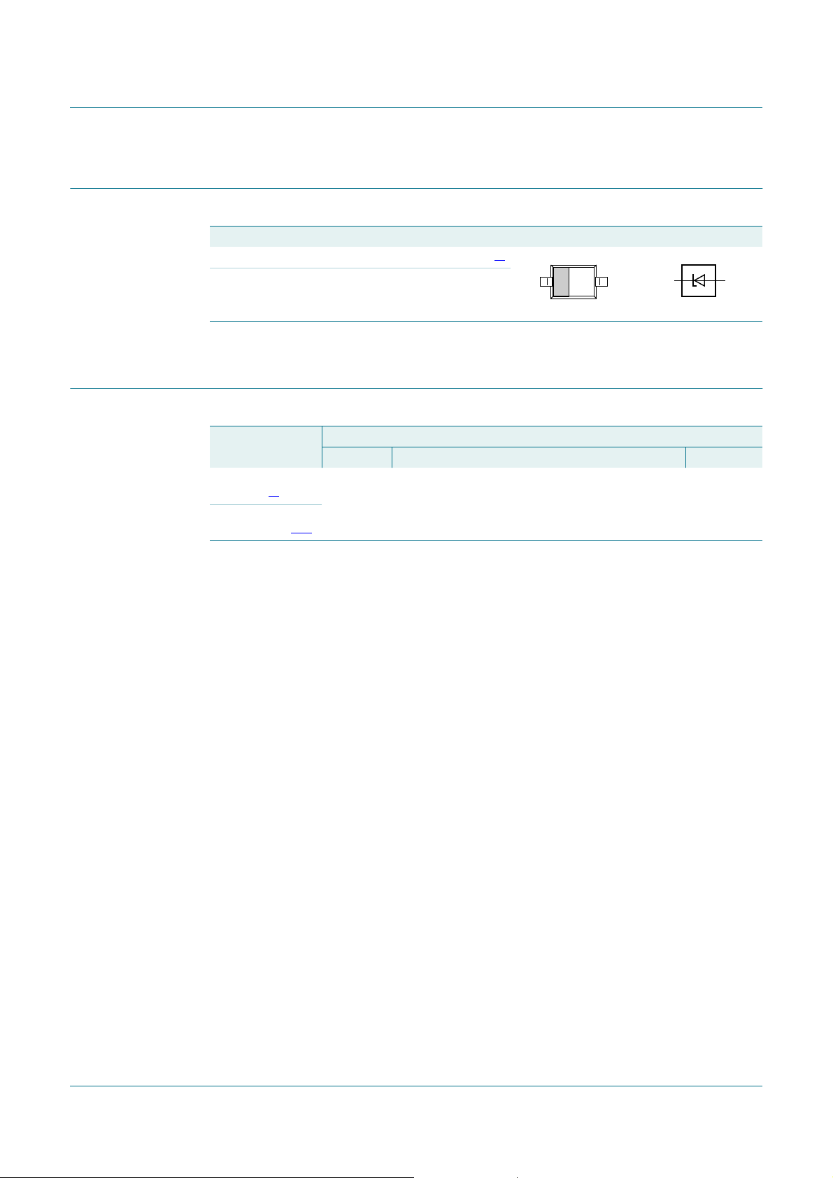
2. Pinning information
Table 2. Pinning
Pin Description Simplified outline Graphic symbol
1 cathode
2 anode
[1] The marking bar indicates the cathode.
3. Ordering information
Table 3. Ordering information
Type number Package
PZU2.4BA to
PZU36BA
PZU2.4BA/DG to
PZU36BA/DG
[1]
PZUxBA series
Single Zener diodes
[1]
21
Name Description Version
SC-76 plastic surface-mounted package; 2 leads SOD323
[1][2]
1
2
006aaa152
[1] The series consists of 97 types with nominal working voltages from 2.4 V to 36 V.
[2] /DG: halogen-free
PZUXBA_SER_1 © NXP B.V. 2008. All rights reserved.
Product data sheet Rev. 01 — 19 September 2008 2 of 14
NXP Semiconductors
4. Marking
Table 4. Marking codes
Type number
PZU2.4*A X8 - - - PZU2.4*A/DG Y8 - - PZU2.7*A X9 XA XB - PZU2.7*A/DG Y9 YA YB PZU3.0*A XT XU XV - PZU3.0*A/DG YT YU YV PZU3.3*A XW XX XY - PZU3.3*A/DG YW YX YY PZU3.6*A XZ MC MD - PZU3.6*A/DG YZ NC ND PZU3.9*A ME MF MG - PZU3.9*A/DG NE NF NG PZU4.3*A MM MN MP MR PZU4.3*A/DG NM NN NP NR
PZU4.7*A MS MT MU MV PZU4.7*A/DG NS NT NU NV
PZU5.1*A MW MX MY MZ PZU5.1*A/DG NW NX NY NZ
PZU5.6*A LF LG LH LK PZU5.6*A/DG RF RG RH RK
PZU6.2*A LL LM LN LP PZU6.2*A/DG RL RM RN RP
PZU6.8*A LR LS LT LU PZU6.8*A/DG RR RS RT RU
PZU7.5*A LV LW LX LY PZU7.5*A/DG RV RW RX RY
PZU8.2*A LZ CR CS CT PZU8.2*A/DG RZ ER ES ET
PZU9.1*A CU CV CW CX PZU9.1*A/DG EU EV EW EX
PZU10*A VA VB VC VD PZU10*A/DG WA WB WC WD
PZU11*A VE VF VG VH PZU11*A/DG WE WF WG WH
PZU12*A VK VL VM VN PZU12*A/DG WK WL WM WN
PZU13*A VP VR VS VT PZU13*A/DG WP WR WS WT
PZU14*A - - VU - PZU14*A/DG - - WU PZU15*A VV VW VX VY PZU15*A/DG WV WW WX WY
PZU16*A VZ X1 X2 X3 PZU16*A/DG WZ Y1 Y2 Y3
PZU18*A X4 X5 X6 X7 PZU18*A/DG Y4 Y5 Y6 Y7
PZU20*A XC XD XE XF PZU20*A/DG YC YD YE YF
PZU22*A XG XH XK XL PZU22*A/DG YG YH YK YL
PZU24*A XM XN XP XR PZU24*A/DG YM YN YP YR
PZU27*A XS - - - PZU27*A/DG YS - - PZU30*A MH - - - PZU30*A/DG NH - - PZU33*A MK - - - PZU33*A/DG NK - - PZU36*A ML - - - PZU36*A/DG NL - - -
PZUxBA series
Single Zener diodes
[1]
Marking code Type number
B B1 B2 B3 B B1 B2 B3
[1]
Marking code
[1] * = B: tolerance series B, approximately ±5%
* = B1, B2, B3: tolerance series B1, B2, B3: approximately ±2%
PZUXBA_SER_1 © NXP B.V. 2008. All rights reserved.
Product data sheet Rev. 01 — 19 September 2008 3 of 14
NXP Semiconductors
5. Limiting values
Table 5. Limiting values
In accordance with the Absolute Maximum Rating System (IEC 60134).
Symbol Parameter Conditions Min Max Unit
I
F
I
ZSM
P
ZSM
P
tot
T
j
T
amb
T
stg
[1] tp= 100 µs; square wave; Tj=25°C prior to surge
[2] Device mounted on an FR4 PCB, single-sided copper, tin-plated and standard footprint.
[3] Device mounted on an FR4 PCB, single-sided copper, tin-plated, mounting pad for cathode 1 cm2.
PZUxBA series
Single Zener diodes
forward current - 200 mA
non-repetitive peak reverse
current
non-repetitive peak reverse
power dissipation
total power dissipation T
amb
≤ 25 °C
junction temperature - 150 °C
ambient temperature −55 +150 °C
storage temperature −65 +150 °C
[1]
- see
Table 8
and
9
[1]
-40W
[2]
- 320 mW
[3]
- 490 mW
6. Thermal characteristics
Table 6. Thermal characteristics
Symbol Parameter Conditions Min Typ Max Unit
R
th(j-a)
thermal resistance from
junction to ambient
R
th(j-sp)
thermal resistance from
junction to solder point
[1] Device mounted on an FR4 PCB, single-sided copper, tin-plated and standard footprint.
[2] Device mounted on an FR4 PCB, single-sided copper, tin-plated, mounting pad for cathode 1 cm2.
[3] Soldering point of cathode tab.
7. Characteristics
Table 7. Characteristics
Tj=25°C unless otherwise specified.
Symbol Parameter Conditions Min Typ Max Unit
V
F
[1] Pulse test: tp≤ 300 µs; δ≤0.02.
forward voltage
in free air
[1]
- - 390 K/W
[2]
- - 255 K/W
[3]
--55K/W
[1]
IF= 10 mA - - 0.9 V
= 100 mA - - 1.1 V
I
F
PZUXBA_SER_1 © NXP B.V. 2008. All rights reserved.
Product data sheet Rev. 01 — 19 September 2008 4 of 14

NXP Semiconductors
PZUxBA series
Single Zener diodes
Table 8. Characteristics per type; PZU2.4BA to PZU5.6B3A and PZU2.4BA/DG to PZU5.6B3A/DG
Tj=25°C unless otherwise specified.
PZUxBA Sel Working
voltage
V
(V)
Z
IZ=5mA IZ= 0.5 mA IZ=5mA IZ=5mA
Min Max Max Max Max VR(V) Typ Max Max
2.4 B 2.3 2.6 1000 100 50 1 −1.6 450 8
2.7 B 2.5 2.9 1000 100 20 1 −2.0 440 8
B1 2.5 2.75
B2 2.65 2.9
3.0 B 2.8 3.2 1000 95 10 1 −2.1 425 8
B1 2.8 3.05
B2 2.95 3.2
3.3 B 3.1 3.5 1000 95 5 1 −2.4 410 8
B1 3.1 3.35
B2 3.25 3.5
3.6 B 3.4 3.8 1000 90 5 1 −2.4 390 8
B1 3.4 3.65
B2 3.55 3.8
3.9 B 3.7 4.1 1000 90 3 1 −2.5 370 8
B1 3.7 3.97
B2 3.87 4.10
4.3 B 4.01 4.48 1000 90 3 1 −2.5 350 8
B1 4.01 4.21
B2 4.15 4.34
B3 4.28 4.48
4.7 B 4.42 4.9 800 80 2 1 −1.4 325 8
B1 4.42 4.61
B2 4.55 4.75
B3 4.69 4.9
5.1 B 4.84 5.37 250 60 2 1.5 0.3 300 5.5
B1 4.84 5.04
B2 4.98 5.2
B3 5.14 5.37
5.6 B 5.31 5.92 100 40 1 2.5 1.9 275 5.5
B1 5.31 5.55
B2 5.49 5.73
B3 5.67 5.92
Differentialresistance
r
(Ω)
dif
Reverse
current
I
(µA)
R
Temperature
coefficient
S
(mV/K)
Z
Diode
capacitance
d
(pF)
[1]
C
Non-repetitive
peak reverse
current
ZSM
(A)
[2]
I
[1] f = 1 MHz; VR=0V
[2] tp= 100 µs; square wave; Tj=25°C prior to surge
PZUXBA_SER_1 © NXP B.V. 2008. All rights reserved.
Product data sheet Rev. 01 — 19 September 2008 5 of 14

NXP Semiconductors
PZUxBA series
Single Zener diodes
Table 9. Characteristics per type; PZU6.2BA to PZU36BA and PZU6.2BA/DG to PZU36BA/DG
Tj=25°C unless otherwise specified.
PZUxBA Sel Working
voltage
V
(V)
Z
IZ=5mA IZ= 0.5 mA IZ=5mA IZ=5mA
Min Max Max Max Max VR(V) Typ Max Max
6.2 B 5.86 6.53 80 30 500 3 2.7 250 5.5
B1 5.86 6.12
B2 6.06 6.33
B3 6.26 6.53
6.8 B 6.47 7.14 60 20 500 3.5 3.4 215 5.5
B1 6.47 6.73
B2 6.65 6.93
B3 6.86 7.14
7.5 B 7.06 7.84 60 10 500 4 4.0 170 3.5
B1 7.06 7.36
B2 7.28 7.60
B3 7.52 7.84
8.2 B 7.76 8.64 60 10 500 5 4.6 150 3.5
B1 7.76 8.1
B2 8.02 8.36
B3 8.28 8.64
9.1 B 8.56 9.55 60 10 500 6 5.5 120 3.5
B1 8.56 8.93
B2 8.85 9.23
B3 9.15 9.55
10 B 9.45 10.55 60 10 100 7 6.4 110 3.5
B1 9.45 9.87
B2 9.77 10.21
B3 10.11 10.55
11 B 10.44 11.56 60 10 100 8 7.4 108 3
B1 10.44 10.88
B2 10.76 11.22
B3 11.1 11.56
12 B 11.42 12.6 80 10 100 9 8.4 105 3
B1 11.42 11.9
B2 11.74 12.24
B3 12.08 12.6
13 B 12.47 13.96 80 10 100 10 9.4 103 2.5
B1 12.47 13.03
B2 12.91 13.49
B3 13.37 13.96
Differentialresistance
r
(Ω)
dif
Reverse
current
I
(nA)
R
Temperature
coefficient
S
(mV/K)
Z
Diode
capacitance
d
(pF)
[1]
C
Non-repetitive
peak reverse
current
ZSM
(A)
[2]
I
PZUXBA_SER_1 © NXP B.V. 2008. All rights reserved.
Product data sheet Rev. 01 — 19 September 2008 6 of 14

NXP Semiconductors
PZUxBA series
Single Zener diodes
Table 9. Characteristics per type; PZU6.2BA to PZU36BA and PZU6.2BA/DG to PZU36BA/DG
…continued
Tj=25°C unless otherwise specified.
PZUxBA Sel Working
voltage
V
(V)
Z
Differentialresistance
r
(Ω)
dif
Reverse
current
I
(nA)
R
Temperature
coefficient
S
(mV/K)
Z
Diode
capacitance
d
(pF)
[1]
C
IZ=5mA IZ= 0.5 mA IZ=5mA IZ=5mA
Min Max Max Max Max VR(V) Typ Max Max
14 B2 13.70 14.30 80 10 100 11 10.4 101 2
15 B 13.84 15.52 80 15 50 11 11.4 99 2
B1 13.84 14.46
B2 14.34 14.98
B3 14.85 15.52
16 B 15.37 17.09 80 20 50 12 12.4 97 1.5
B1 15.37 16.01
B2 15.85 16.51
B3 16.35 17.09
18 B 16.94 19.03 80 20 50 13 14.4 93 1.5
B1 16.94 17.7
B2 17.56 18.35
B3 18.21 19.03
20 B 18.86 21.08 100 20 50 15 16.4 88 1.5
B1 18.86 19.7
B2 19.52 20.39
B3 20.21 21.08
22 B 20.88 23.17 100 25 50 17 18.4 84 1.3
B1 20.88 21.77
B2 21.54 22.47
B3 22.23 23.17
24 B 22.93 25.57 120 30 50 19 20.4 80 1.3
B1 22.93 23.96
B2 23.72 24.78
B3 24.54 25.57
27 B 25.1 28.9 150 40 50 21 23.4 73 1
30 B 28 32 200 40 50 23 26.6 66 1
33 B 31 35 250 40 50 25 29.7 60 0.9
36 B 34 38 300 60 50 27 33.0 59 0.8
Non-repetitive
peak reverse
current
ZSM
(A)
[2]
I
[1] f = 1 MHz; VR=0V
[2] tp= 100 µs; square wave; Tj=25°C prior to surge
PZUXBA_SER_1 © NXP B.V. 2008. All rights reserved.
Product data sheet Rev. 01 — 19 September 2008 7 of 14
NXP Semiconductors
PZUxBA series
Single Zener diodes
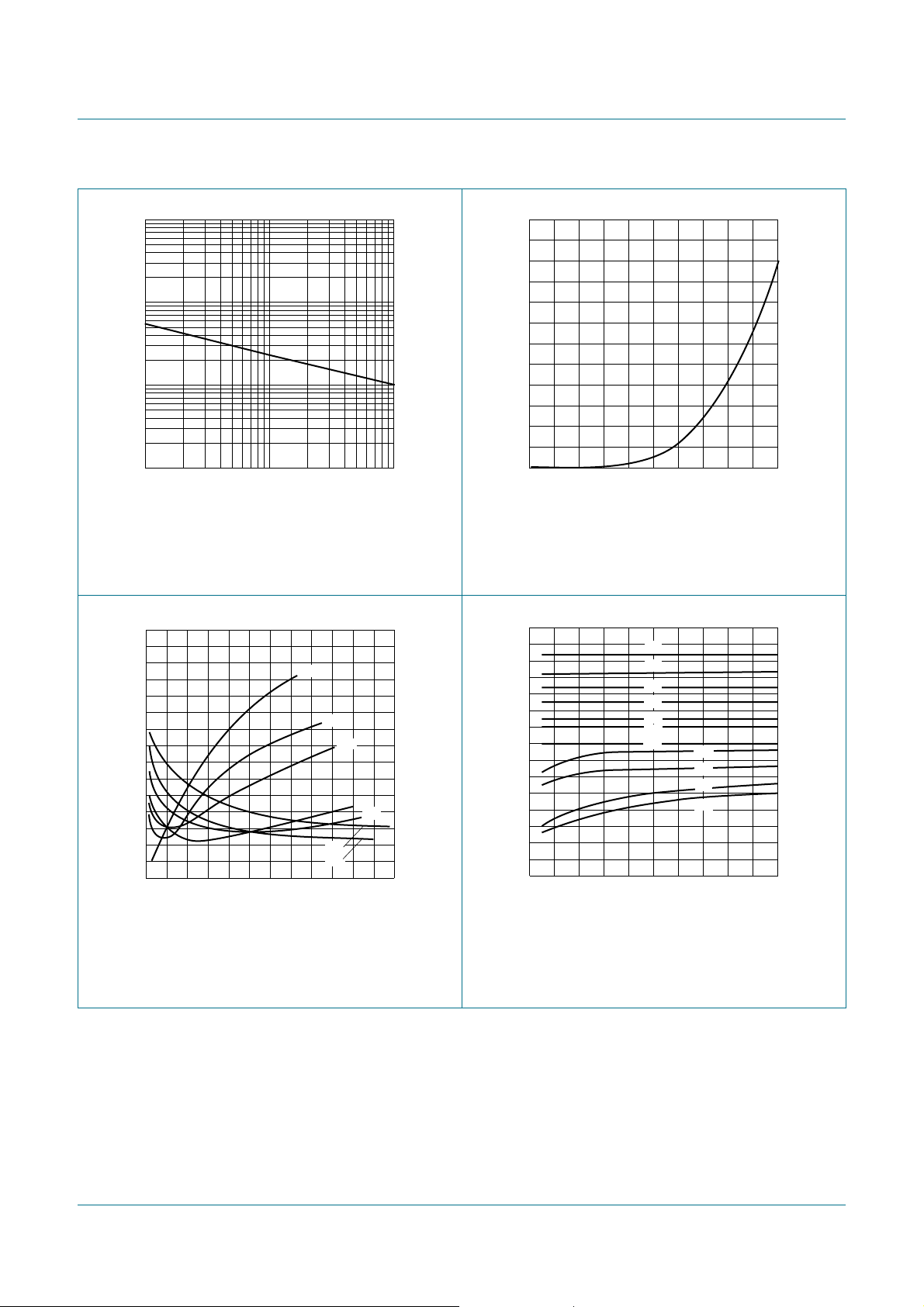
t
p
(s)
006aab215
10
−2
P
(W)
ZSM
3
10
2
10
10
1
−4
10
−3
10
Tj=25°C (prior to surge) Tj=25°C
Fig 1. Non-repetitive peak reverse power dissipation
as a function of pulse duration; maximum
values
mgl273
3.9
3.6
3.3
3.0
S
Z
(mV/K)
0
4.3
−1
−2
300
I
F
(mA)
200
100
0
0.6 10.8
mbg781
VF (V)
Fig 2. Forward current as a function of forward
voltage; typical values
mgl274
S
Z
(mV/K)
10
12
11
10
5
0
9.1
8.2
7.5
6.8
6.2
5.6
5.1
4.7
2.4
2.7
−3
060
20 40
I
Z
(mA)
Tj=25°C to 150 °C
VZ= 2.4 V to 4.3 V
Fig 3. Temperature coefficient as a function of
working current; typical values
PZUXBA_SER_1 © NXP B.V. 2008. All rights reserved.
−5
02016
4812
IZ (mA)
Tj=25°C to 150 °C
VZ= 4.7 V to 12 V
Fig 4. Temperature coefficient as a function of
working current; typical values
Product data sheet Rev. 01 — 19 September 2008 8 of 14

NXP Semiconductors
PZUxBA series
Single Zener diodes
3.0
3.3
006aab246
3.6
3.9
VZ (V)
4.3
I
Z
(mA)
10
10
10
2
10
10
1
−1
−2
−3
054231
V
Z(nom)
(V) = 2.4
2.7
Tj=25°C
VZ= 2.4 V to 4.3 V
Fig 5. Working current as a function of working
voltage; typical values
2
10
I
V
(mA)
Z
10
1
Z(nom)
14
15
16
(V) = 13
182022
10
006aab247
11
12
VZ (V)
2
10
V
I
Z(nom)
Z
(mA)
10
1
−1
10
−2
10
−3
10
01410 128624
(V) = 4.7
5.1
5.6
6.2
6.8
9.1
8.2
7.5
Tj=25°C
VZ= 4.7 V to 12 V
Fig 6. Working current as a function of working
voltage; typical values
006aab248
27
24
33
30
36
−1
10
−2
10
−3
10
10 403020
VZ (V)
Tj=25°C
VZ= 13 V to 36 V
Fig 7. Working current as a function of working voltage; typical values
PZUXBA_SER_1 © NXP B.V. 2008. All rights reserved.
Product data sheet Rev. 01 — 19 September 2008 9 of 14
NXP Semiconductors
8. Test information
8.1 Quality information
This product has been qualified in accordance with the Automotive Electronics Council
(AEC) standard
suitable for use in automotive applications.
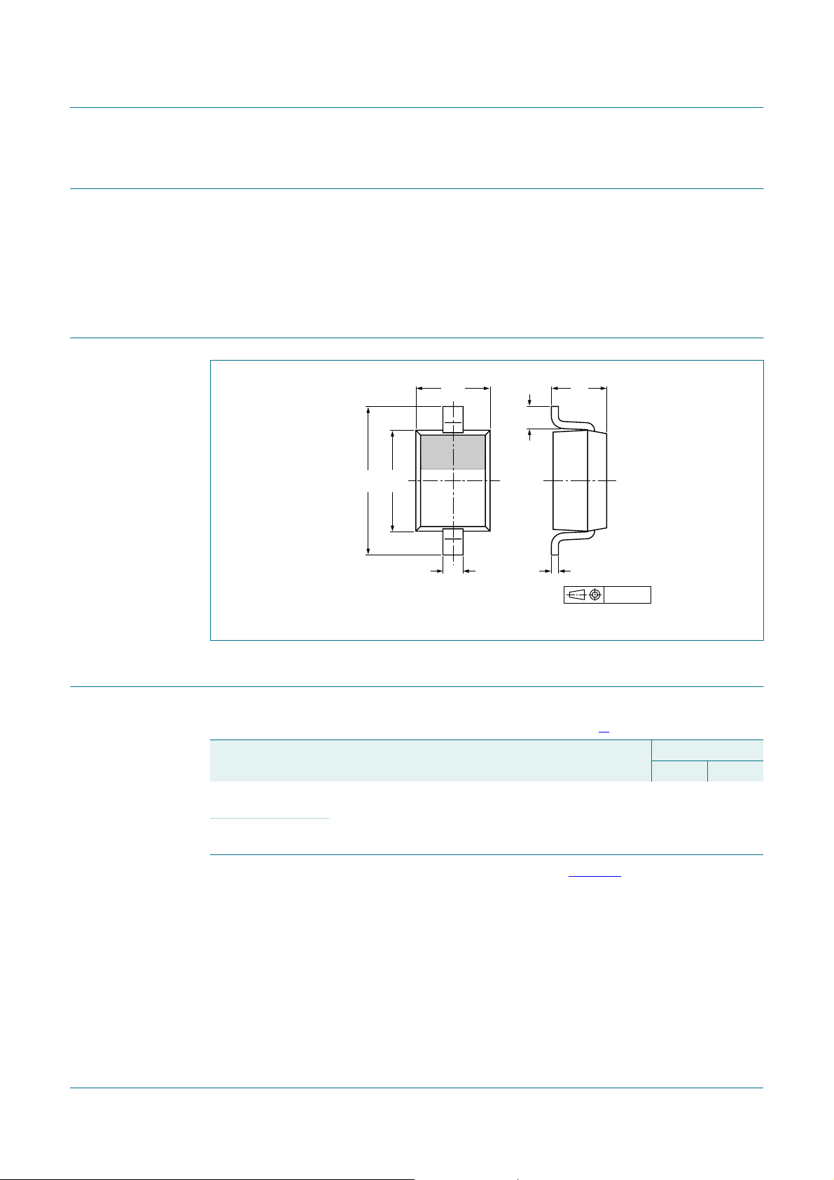
9. Package outline
PZUxBA series
Single Zener diodes
Q101 - Stress test qualification for discrete semiconductors
, and is
Fig 8. Package outline SOD323 (SC-76)
10. Packing information
Table 10. Packing methods
The indicated -xxx are the last three digits of the 12NC ordering code.
Type number Package Description Packing quantity
PZU2.4BA to
PZU36BA
PZU2.4BA/DG to
PZU36BA/DG
1.1
0.8
0.25
0.10
03-12-17Dimensions in mm
[1]
2.7
2.3
1.8
1.6
1.35
1.15
1
2
0.40
0.25
0.45
0.15
3000 10000
SOD323 4 mm pitch, 8 mm tape and reel -115 -135
[1] For further information and the availability of packing methods, seeSection 13.
PZUXBA_SER_1 © NXP B.V. 2008. All rights reserved.
Product data sheet Rev. 01 — 19 September 2008 10 of 14
NXP Semiconductors
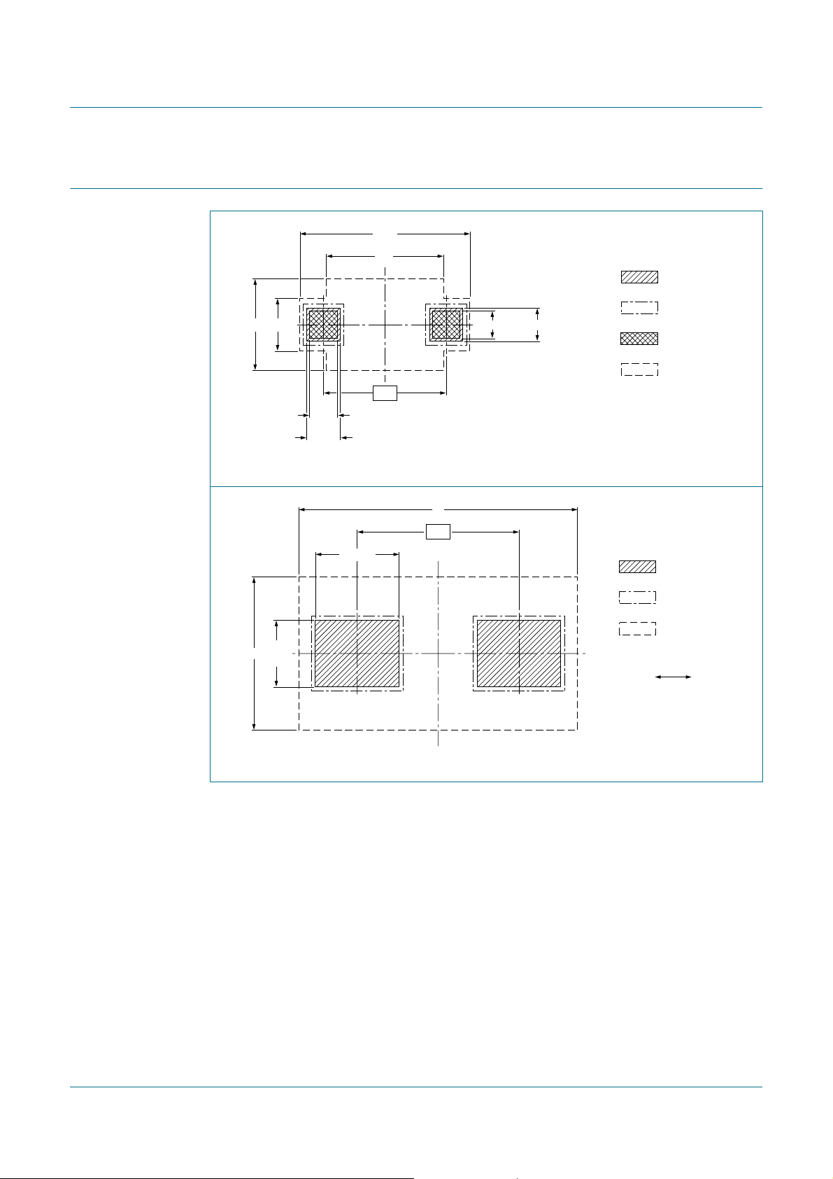
11. Soldering
PZUxBA series
Single Zener diodes
3.05
2.1
solder lands
solder resist
0.951.65
0.6 (2×)0.5 (2×)
solder paste
occupied area
2.2
0.5
(2×)
0.6
(2×)
Fig 9. Reflow soldering footprint SOD323 (SC-76)
5
2.9
1.5 (2×)
1.2
2.75
(2×)
Fig 10. Wave soldering footprint SOD323 (SC-76)
Dimensions in mm
sod323_fr
solder lands
solder resist
occupied area
Dimensions in mm
preferred transport
direction during soldering
sod323_fw
PZUXBA_SER_1 © NXP B.V. 2008. All rights reserved.
Product data sheet Rev. 01 — 19 September 2008 11 of 14

NXP Semiconductors
PZUxBA series
Single Zener diodes
12. Revision history
Table 11. Revision history
Document ID Release date Data sheet status Change notice Supersedes
PZUXBA_SER_1 20080919 Product data sheet - -
PZUXBA_SER_1 © NXP B.V. 2008. All rights reserved.
Product data sheet Rev. 01 — 19 September 2008 12 of 14

NXP Semiconductors
13. Legal information
13.1 Data sheet status
PZUxBA series
Single Zener diodes
Document status
Objective [short] data sheet Development This document contains data from the objective specification for product development.
Preliminary [short] data sheet Qualification This document contains data from the preliminary specification.
Product [short] data sheet Production This document contains the product specification.
[1] Please consult the most recently issued document before initiating or completing a design.
[2] The term ‘short data sheet’ is explained in section “Definitions”.
[3] The product status of device(s) described in this document may have changed since this document was published and may differ in case of multiple devices. The latest product status
information is available on the Internet at URL
[1][2]
Product status
13.2 Definitions
Draft — The document is a draft version only. The content is still under
internal review and subject to formal approval, which may result in
modifications or additions. NXP Semiconductors does not give any
representations or warranties as to the accuracy or completeness of
information included herein and shall haveno liability for the consequences of
use of such information.
Short data sheet — A short data sheet is an extract from a full data sheet
with the same product type number(s)and title. A short data sheet is intended
for quick reference only and should not be relied upon to contain detailed and
full information. For detailed and full information see the relevant full data
sheet, which is available on request via the local NXP Semiconductors sales
office. In case of any inconsistency or conflict with the short data sheet, the
full data sheet shall prevail.
13.3 Disclaimers
General — Information in this document is believed to be accurate and
reliable. However, NXP Semiconductors does not give any representations or
warranties, expressed or implied, as to the accuracy or completeness of such
information and shall have no liability for the consequences of use of such
information.
Right to make changes — NXP Semiconductors reserves the right to make
changes to information published in this document, including without
limitation specifications and product descriptions, at any time and without
notice. This document supersedes and replaces all information supplied prior
to the publication hereof.
Suitability for use — NXP Semiconductors products are not designed,
authorized or warranted to be suitable for use in medical, military, aircraft,
space or life support equipment, nor in applications where failure or
malfunction of an NXP Semiconductors product can reasonably be expected
to result in personal injury, death or severe property or environmental
[3]
http://www.nxp.com.
Definition
damage. NXP Semiconductors accepts no liability for inclusion and/or use of
NXP Semiconductors products in such equipment or applications and
therefore such inclusion and/or use is at the customer’s own risk.
Applications — Applications that are described herein for any of these
products are for illustrative purposes only. NXP Semiconductors makes no
representation or warranty that such applications will be suitable for the
specified use without further testing or modification.
Limiting values — Stress above one or more limiting values (as defined in
the Absolute Maximum Ratings System of IEC 60134) may cause permanent
damage to the device. Limiting valuesare stress ratings only and operation of
the device at these or any other conditions above those given in the
Characteristics sections of this document is not implied. Exposure to limiting
values for extended periods may affect device reliability.
Terms and conditions of sale — NXP Semiconductors products are sold
subject to the general terms and conditions of commercial sale, as published
at
http://www.nxp.com/profile/terms, including those pertaining to warranty,
intellectual property rights infringement and limitation of liability, unless
explicitly otherwise agreed to in writing by NXP Semiconductors. In case of
any inconsistency or conflict between information in this document and such
terms and conditions, the latter will prevail.
No offer to sell or license — Nothing in this document may be interpreted
or construed as an offer to sell products that is open for acceptance or the
grant, conveyance or implication of any license under any copyrights, patents
or other industrial or intellectual property rights.
Quick reference data — The Quick reference data is an extract of the
product data given in the Limiting values and Characteristics sections of this
document, and as such is not complete, exhaustive or legally binding.
13.4 Trademarks
Notice: All referenced brands, productnames, service names and trademarks
are the property of their respective owners.
14. Contact information
For more information, please visit: http://www.nxp.com
For sales office addresses, please send an email to: salesaddresses@nxp.com
PZUXBA_SER_1 © NXP B.V. 2008. All rights reserved.
Product data sheet Rev. 01 — 19 September 2008 13 of 14

NXP Semiconductors
15. Contents
1 Product profile . . . . . . . . . . . . . . . . . . . . . . . . . . 1
1.1 General description. . . . . . . . . . . . . . . . . . . . . . 1
1.2 Features . . . . . . . . . . . . . . . . . . . . . . . . . . . . . . 1
1.3 Applications . . . . . . . . . . . . . . . . . . . . . . . . . . . 1
1.4 Quick reference data. . . . . . . . . . . . . . . . . . . . . 1
2 Pinning information. . . . . . . . . . . . . . . . . . . . . . 2
3 Ordering information. . . . . . . . . . . . . . . . . . . . . 2
4 Marking . . . . . . . . . . . . . . . . . . . . . . . . . . . . . . . . 3
5 Limiting values. . . . . . . . . . . . . . . . . . . . . . . . . . 4
6 Thermal characteristics. . . . . . . . . . . . . . . . . . . 4
7 Characteristics. . . . . . . . . . . . . . . . . . . . . . . . . . 4
8 Test information. . . . . . . . . . . . . . . . . . . . . . . . 10
8.1 Quality information . . . . . . . . . . . . . . . . . . . . . 10
9 Package outline . . . . . . . . . . . . . . . . . . . . . . . . 10
10 Packing information. . . . . . . . . . . . . . . . . . . . . 10
11 Soldering . . . . . . . . . . . . . . . . . . . . . . . . . . . . . 11
12 Revision history. . . . . . . . . . . . . . . . . . . . . . . . 12
13 Legal information. . . . . . . . . . . . . . . . . . . . . . . 13
13.1 Data sheet status . . . . . . . . . . . . . . . . . . . . . . 13
13.2 Definitions. . . . . . . . . . . . . . . . . . . . . . . . . . . . 13
13.3 Disclaimers. . . . . . . . . . . . . . . . . . . . . . . . . . . 13
13.4 Trademarks. . . . . . . . . . . . . . . . . . . . . . . . . . . 13
14 Contact information. . . . . . . . . . . . . . . . . . . . . 13
15 Contents . . . . . . . . . . . . . . . . . . . . . . . . . . . . . . 14
PZUxBA series
Single Zener diodes
Please be aware that important notices concerning this document and the product(s)
described herein, have been included in section ‘Legal information’.
© NXP B.V. 2008. All rights reserved.
For more information, please visit: http://www.nxp.com
For sales office addresses, please send an email to: salesaddresses@nxp.com
Date of release: 19 September 2008
Document identifier: PZUXBA_SER_1

 Loading...