

132
4
56
S
1
D
1
G1S
2
msd901
D
2
G
2
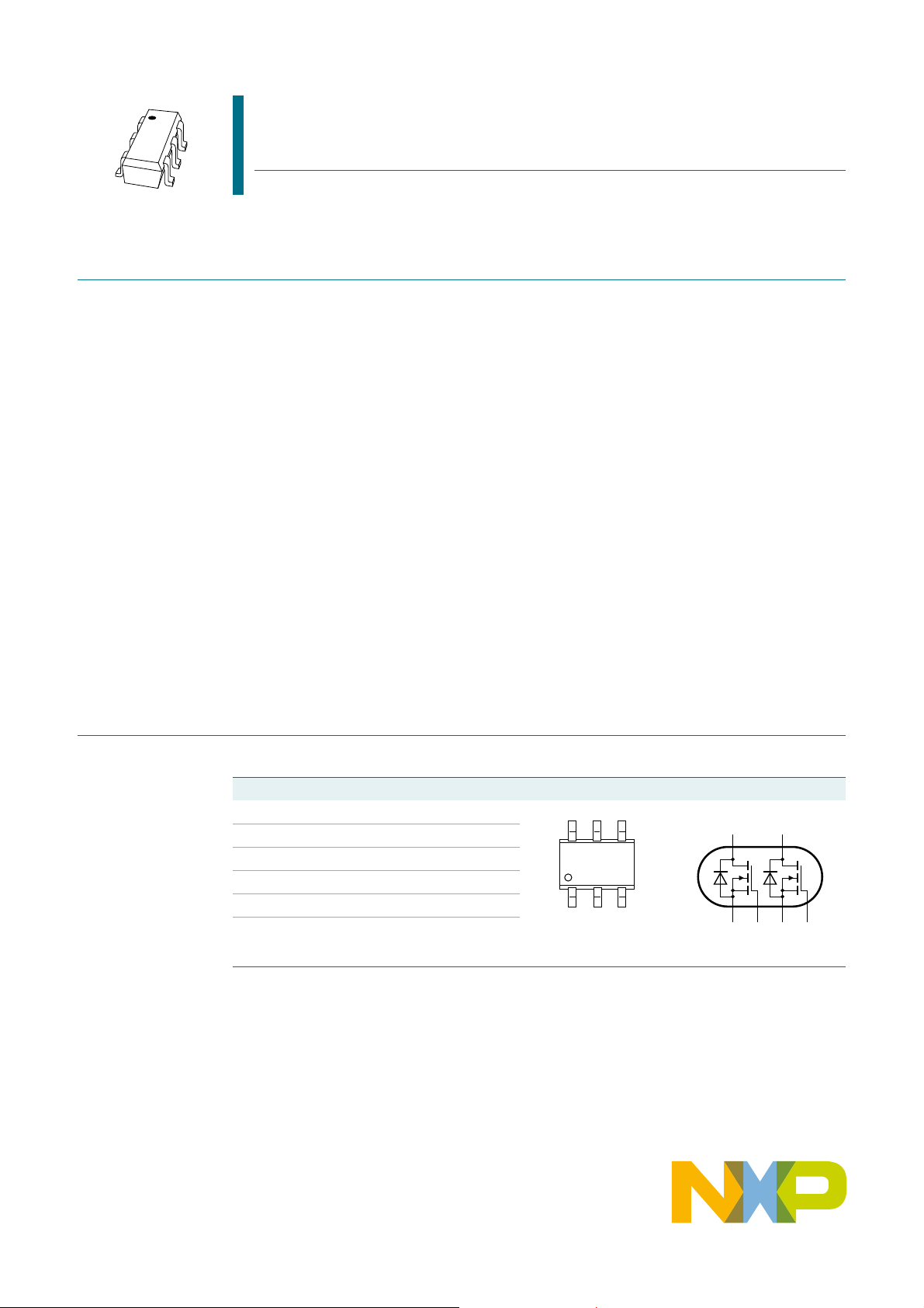
PMGD780SN
Dual N-channel μTrenchMOS standard level FET
Rev. 02 — 19 April 2010 Product data sheet
1. Product profile
1.1 General description
Dual N-channel enhancement mode field-effect transistor in a small SOT363 (SC-88)
Surface-Mounted Device (SMD) plastic package using TrenchMOS technology.
1.2 Features and benefits
Surface-mounted package Footprint 40 % smaller than SOT23
Standard level threshold voltage Fast switching
Low on-state resistance Dual device
1.3 Applications
Driver circuits Switching in portable appliances
1.4 Quick reference data
V
P
≤ 60 V ID≤ 0.49 A
DS
≤ 0.41 W R
tot
2. Pinning information
Table 1. Pinning - SOT363 (SC-88), simplified outline and symbol
Pin Description Simplified outline Graphic symbol
1 source1 (S1)
2 gate1 (G1)
3 drain2 (D2)
4 source2 (S2)
5 gate2 (G2)
6 drain1 (D1)
≤ 920 mΩ
DSon
SOT363 (SC-88)
NXP Semiconductors
3. Ordering information
PMGD780SN
Dual N-channel μTrenchMOS standard level FET
Table 2. Ordering information
Type number Package
PMGD780SN SC-88 plastic surface-mounted package; 6 leads SOT363
Name Description Ver s ion
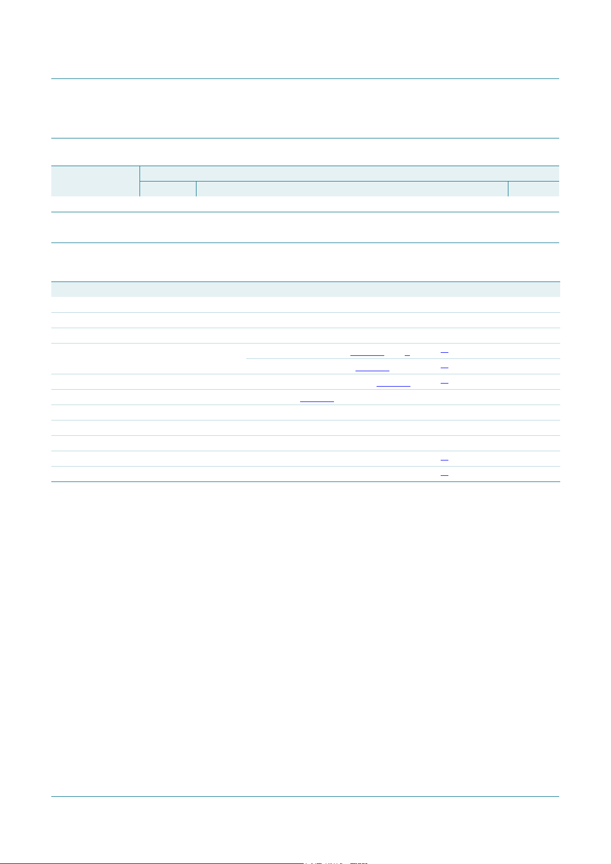
4. Limiting values
Table 3. Limiting values
In accordance with the Absolute Maximum Rating System (IEC 60134).
Symbol Parameter Conditions Min Max Unit
V
DS
V
DGR
V
GS
I
D
I
DM
P
tot
T
stg
T
j
Source-drain diode
I
S
I
SM
drain-source voltage 25 °C ≤ Tj≤ 150 °C-60V
drain-gate voltage 25 °C ≤ Tj≤ 150 °C; RGS=20kΩ -60V
gate-source voltage - ±20 V
drain current Tsp=25°C; VGS=10V; Figure 2 and 3
peak drain current Tsp=25°C; pulsed; tp≤ 10 μs; Figure 3
total power dissipation Tsp=25°C; Figure 1 -0.41W
storage temperature −55 +150 °C
junction temperature −55 +150 °C
source current Tsp=25°C
peak source current Tsp=25°C; pulsed; tp≤ 10 μs
[1]
-0.49A
=100°C; VGS=10V; Figure 2
T
sp
[1]
-0.31A
[1]
-0.99A
[1]
-0.34A
[1]
-0.69A
[1] Single device conducting.
PMGD780SN_2 All information provided in this document is subject to legal disclaimers. © NXP B.V. 2010. All rights reserved.
Product data sheet Rev. 02 — 19 April 2010 2 of 14
NXP Semiconductors
Tsp (°C)
0 20015050 100
03aa17
40
80
120
P
der
(%)
0
Tsp (°C)
0 20015050 100
03aa25
40
80
120
I
der
(%)
0
P
der
P
tot
P
tot 25 C°()
------------ -----------
100%×=
I
der
I
D
I
D25C
°
()
------------ -------
100%×=
03an22
10
-3
10
-2
10
-1
1
10
10
-1
1 10 10
2
VDS(V)
I
D
(A)
DC
10 ms
Limit R
DSon
= V
DS
/ I
D
1 ms
tp = 10 μs
100 ms
100 μs
PMGD780SN
Dual N-channel μTrenchMOS standard level FET
Fig 1. Normalized total power dissipation as a
function of solder point temperature
Fig 2. Normalized continuous drain current as a
function of solder point temperature
Tsp=25°C; IDM is single pulse; VGS=10V
Fig 3. Safe operating area; continuous and peak drain currents as a function of drain-source voltage
PMGD780SN_2 All information provided in this document is subject to legal disclaimers. © NXP B.V. 2010. All rights reserved.
Product data sheet Rev. 02 — 19 April 2010 3 of 14
NXP Semiconductors
03an28
1
10
10
2
10
3
10
-4
10
-3
10
-2
10
-1
1 10
tp (s)
Z
th(j-sp)
(K/W)
single pulse
δ
= 0.5
0.2
0.1
0.05
0.02
t
p
t
p
T
P
t
T
δ =
5. Thermal characteristics
PMGD780SN
Dual N-channel μTrenchMOS standard level FET
Table 4. Thermal characteristics
Symbol Parameter Conditions Min Typ Max Unit
R
th(j-sp)
thermal resistance from junction to solder point Figure 4 - - 300 K/W
Fig 4. Transient thermal impedance from junction to solder point as a function of pulse duration
PMGD780SN_2 All information provided in this document is subject to legal disclaimers. © NXP B.V. 2010. All rights reserved.
Product data sheet Rev. 02 — 19 April 2010 4 of 14
NXP Semiconductors
6. Characteristics
PMGD780SN
Dual N-channel μTrenchMOS standard level FET
Table 5. Characteristics
=25°C unless otherwise specified.
T
j
Symbol Parameter Conditions Min Typ Max Unit
Static characteristics
V
(BR)DSS
V
GS(th)
drain-source breakdown voltage ID= 250 μA; VGS=0V
=25°C 60--V
T
j
= −55 °C 55--V
T
j
gate-source threshold voltage ID= 0.25 mA; VDS=VGS; Figure 9
Tj=25°C 122.5V
=150°C0.6−−V
T
j
= −55 °C −−3.5 V
T
j
I
DSS
I
GSS
R
DSon
drain leakage current VDS=60V; VGS=0V
=25°C-0.051μA
T
j
=150°C - - 100 μA
T
j
gate leakage current VGS= ±20 V; VDS= 0 V - 10 100 nA
drain-source on-state resistance VGS=10V; ID=0.3A; Figure 7 and 8
Tj=25°C - 780 920 mΩ
=150°C - 1445 1700 mΩ
T
V
GS
j
= 4.5 V; ID=0.075A; Figure 7 and 8 -11001400mΩ
Dynamic characteristics
Q
Q
Q
C
C
C
t
d(on)
t
r
t
d(off)
t
f
G(tot)
GS
GD
iss
oss
rss
total gate charge ID=1A; VDD=30V; VGS=10V; Figure 13 -1.05-nC
gate-source charge - 0.2 - nC
gate-drain charge - 0.22 - nC
input capacitance VGS=0V; VDS= 30 V; f = 1 MHz; Figure 11 -23-pF
output capacitance - 5 - pF
reverse transfer capacitance - 3.5 - pF
turn-on delay time VDD=30V; RL=30Ω; VGS=10V; RG=6Ω -2-ns
rise time -4-ns
turn-off delay time - 5 - ns
fall time -2.2-ns
Source-drain diode
V
SD
source-drain voltage IS= 0.3 A; VGS=0V; Figure 12 - 0.83 1.2 V
PMGD780SN_2 All information provided in this document is subject to legal disclaimers. © NXP B.V. 2010. All rights reserved.
Product data sheet Rev. 02 — 19 April 2010 5 of 14

NXP Semiconductors
03an88
0
0.5
1
1.5
2
0123
V
DS
(V)
I
D
(A)
10
6
5
3.5
4
4.5
VGS (V) = 3
03an90
0
0.2
0.4
0.6
0.8
1
012345
V
GS
(V)
I
D
(A)
Tj = 150 °C 25 °C
03an89
0
1
2
3
0 0.2 0.4 0.6 0.8 1
I
D
(A)
R
DSon
(Ω)
10
6
5
4
4.5
VGS (V) = 3.5
Tj (°C)
−60 180120060
03aa28
1.2
0.6
1.8
2.4
a
0
a
R
DSon
R
DS o n 25 C°()
------------ -----------------
=
PMGD780SN
Dual N-channel μTrenchMOS standard level FET
Tj=25°CT
Fig 5. Output characteristics: drain current as a
function of drain-source voltage; typical
values
Tj=25°C
=25°C and 150 °C; VDS> ID× R
j
DSon
Fig 6. Transfer characteristics: drain current as a
function of gate-source voltage; typical values
Fig 7. Drain-source on-state resistance as a function
PMGD780SN_2 All information provided in this document is subject to legal disclaimers. © NXP B.V. 2010. All rights reserved.
Product data sheet Rev. 02 — 19 April 2010 6 of 14
of drain current; typical values
Fig 8. Normalized drain-source on-state resistance
as a function of junction temperature

NXP Semiconductors
Tj (°C)
−60 180120060
03aa34
1.2
0.6
1.8
2.4
V
GS(th)
(V)
0
typ
min
03an32
1E-8
1E-7
10
-6
10
-5
10
-4
10
-3
0 0.5 1 1.5 2 2.5
V
GS
(V)
I
D
(A)
min typ
03an92
1
10
10
2
10
-1
1 10 10
2
VDS (V)
C
(pF)
C
iss
C
oss
C
rss
PMGD780SN
Dual N-channel μTrenchMOS standard level FET
ID=0.25mA; VDS=V
GS
Fig 9. Gate-source threshold voltage as a function of
junction temperature
Fig 10. Sub-threshold drain current as a function of
Tj=25°C; VDS=5V
gate-source voltage
VGS=0V; f=1MHz
Fig 11. Input, output and reverse transfer capacitances as a function of drain-source voltage; typical values
PMGD780SN_2 All information provided in this document is subject to legal disclaimers. © NXP B.V. 2010. All rights reserved.
Product data sheet Rev. 02 — 19 April 2010 7 of 14

NXP Semiconductors
03an91
0
0.2
0.4
0.6
0.8
1
0 0.3 0.6 0.9 1.2
V
SD
(V)
I
S
(A)
Tj = 25 °C
150 °C
VGS = 0 V
03an93
0
2
4
6
8
10
0 0.3 0.6 0.9 1.2
Q
G
(nC)
V
GS
(V)
ID = 1 A
T
j
= 25 °C
V
DS
= 30 V
Tj=25°C and 150 °C; VGS=0V ID=1A; VDD=30V
Fig 12. Source current as a function of source-drain
voltage; typical values
PMGD780SN
Dual N-channel μTrenchMOS standard level FET
Fig 13. Gate-source voltage as a function of gate
charge; typical values
PMGD780SN_2 All information provided in this document is subject to legal disclaimers. © NXP B.V. 2010. All rights reserved.
Product data sheet Rev. 02 — 19 April 2010 8 of 14

NXP Semiconductors
REFERENCES
OUTLINE
VERSION
EUROPEAN
PROJECTION
ISSUE DATE
IEC JEDEC JEITA
SOT363 SC-88
wBM
b
p
D
e
1
e
pin 1
index
A
A
1
L
p
Q
detail X
H
E
E
v M
A
AB
y
0 1 2 mm
scale
c
X
132
456
Plastic surface-mounted package; 6 leads SOT363
UNIT
A
1
max
b
p
cD
E
e
1
H
E
L
p
Qywv
mm
0.1
0.30
0.20
2.2
1.8
0.25
0.10
1.35
1.15
0.65
e
1.3
2.2
2.0
0.2 0.10.2
DIMENSIONS (mm are the original dimensions)
0.45
0.15
0.25
0.15
A
1.1
0.8
04-11-08
06-03-16
PMGD780SN
Dual N-channel μTrenchMOS standard level FET
7. Package outline
Fig 14. Package outline SOT363 (SC-88)
PMGD780SN_2 All information provided in this document is subject to legal disclaimers. © NXP B.V. 2010. All rights reserved.
Product data sheet Rev. 02 — 19 April 2010 9 of 14

NXP Semiconductors
solder lands
solder resist
occupied area
solder paste
sot363_fr
2.65
2.35
0.4 (2×)
0.6
(2×)
0.5
(4×)
0.5
(4×)
0.6
(4×)
0.6
(4×)
1.5
1.8
Dimensions in mm
8. Soldering
Fig 15. Reflow soldering footprint SOT363 (SC-88)
PMGD780SN
Dual N-channel μTrenchMOS standard level FET
PMGD780SN_2 All information provided in this document is subject to legal disclaimers. © NXP B.V. 2010. All rights reserved.
Product data sheet Rev. 02 — 19 April 2010 10 of 14

NXP Semiconductors
Dual N-channel μTrenchMOS standard level FET
PMGD780SN
9. Revision history
Table 6. Revision history
Document ID Release date Data sheet status Change notice Supersedes
PMGD780SN_2 20100419 Product data sheet - PMGD780SN_1
Modifications:
PMGD780SN_1 20040211 Product data - -
• The format of this data sheet has been redesigned to comply with the new identity
guidelines of NXP Semiconductors.
• Legal texts have been adapted to the new company name where appropriate.
• Table 5 “Characteristics”: added V
• Section 10 “Legal information”: updated
maximum value at condition Tj=25°C
GS(th)
PMGD780SN_2 All information provided in this document is subject to legal disclaimers. © NXP B.V. 2010. All rights reserved.
Product data sheet Rev. 02 — 19 April 2010 11 of 14

NXP Semiconductors
PMGD780SN
Dual N-channel μTrenchMOS standard level FET
10. Legal information
10.1 Data sheet status
Document status
Objective [short] data sheet Development This document contains data from the objective specification for product development.
Preliminary [short] data sheet Qualification This document contains data from the preliminary specification.
Product [short] data sheet Production This document contains the product specification.
[1] Please consult the most recently issued document before initiating or completing a design.
[2] The term ‘short data sheet’ is explained in section “Definitions”.
[3] The product status of device(s) described in this document may have changed since this document was published and may differ in case of multiple devices. The latest product status
information is available on the Internet at URL http://www.nxp.com
[1][2]
Product status
[3]
Definition
.
10.2 Definitions
Draft — The document is a draft version only. The content is still under
internal review and subject to formal approval, which may result in
modifications or additions. NXP Semiconductors does not give any
representations or warranties as to the accuracy or completeness of
information included herein and shall have no liability for the consequences of
use of such information.
Short data sheet — A short data sheet is an extract from a full data sheet
with the same product type number(s) and title. A short data sheet is intended
for quick reference only and should not be relied upon to contain detailed and
full information. For detailed and full information see the relevant full data
sheet, which is available on request via the local NXP Semiconductors sales
office. In case of any inconsistency or conflict with the short data sheet, the
full data sheet shall prevail.
Product specification — The information and data provided in a Product
data sheet shall define the specification of the product as agreed between
NXP Semiconductors and its customer, unless NXP Semiconductors and
customer have explicitly agreed otherwise in writing. In no event however,
shall an agreement be valid in which the NXP Semiconductors product is
deemed to offer functions and qualities beyond those described in the
Product data sheet.
10.3 Disclaimers
Limited warranty and liability — Information in this document is believed to
be accurate and reliable. However, NXP Semiconductors does not give any
representations or warranties, expressed or implied, as to the accuracy or
completeness of such information and shall have no liability for the
consequences of use of such information.
In no event shall NXP Semiconductors be liable for any indirect, incidental,
punitive, special or consequential damages (including - without limitation - lost
profits, lost savings, business interruption, costs related to the removal or
replacement of any products or rework charges) whether or not such
damages are based on tort (including negligence), warranty, breach of
contract or any other legal theory.
Notwithstanding any damages that customer might incur for any reason
whatsoever, NXP Semiconductors’ aggregate and cumulative liability towards
customer for the products described herein shall be limited in accordance
with the Terms and conditions of commercial sale of NXP Semiconductors.
Right to make changes — NXP Semiconductors reserves the right to make
changes to information published in this document, including without
limitation specifications and product descriptions, at any time and without
notice. This document supersedes and replaces all information supplied prior
to the publication hereof.
Suitability for use — NXP Semiconductors products are not designed,
authorized or warranted to be suitable for use in medical, military, aircraft,
space or life support equipment, nor in applications where failure or
PMGD780SN_2 All information provided in this document is subject to legal disclaimers. © NXP B.V. 2010. All rights reserved.
malfunction of an NXP Semiconductors product can reasonably be expected
to result in personal injury, death or severe property or environmental
damage. NXP Semiconductors accepts no liability for inclusion and/or use of
NXP Semiconductors products in such equipment or applications and
therefore such inclusion and/or use is at the customer’s own risk.
Applications — Applications that are described herein for any of these
products are for illustrative purposes only. NXP Semiconductors makes no
representation or warranty that such applications will be suitable for the
specified use without further testing or modification.
NXP Semiconductors does not accept any liability related to any default,
damage, costs or problem which is based on a weakness or default in the
customer application/use or the application/use of customer ’s third party
customer(s) (hereinafter both referred to as “Application”). It is customer’s
sole responsibility to check whether the NXP Semiconductors product is
suitable and fit for the Application planned. Customer has to do all necessary
testing for the Application in order to avoid a default of the Application and the
product. NXP Semiconductors does not accept any liability in this respect.
Limiting values — Stress above one or more limiting values (as defined in
the Absolute Maximum Ratings System of IEC 60134) will cause permanent
damage to the device. Limiting values are stress ratings only and (proper)
operation of the device at these or any other conditions above those given in
the Recommended operating conditions section (if present) or the
Characteristics sections of this document is not warranted. Constant or
repeated exposure to limiting values will permanently and irreversibly affect
the quality and reliability of the device.
Terms and conditions of commercial sale — NXP Semiconductors
products are sold subject to the general terms and conditions of commercial
sale, as published at http://www.nxp.com/profile/terms
agreed in a valid written individual agreement. In case an individual
agreement is concluded only the terms and conditions of the respective
agreement shall apply. NXP Semiconductors hereby expressly objects to
applying the customer ’s general terms and conditions with regard to the
purchase of NXP Semiconductors products by customer.
No offer to sell or license — Nothing in this document may be interpreted or
construed as an offer to sell products that is open for acceptance or the grant,
conveyance or implication of any license under any copyrights, patents or
other industrial or intellectual property rights.
Export control — This document as well as the item(s) described herein
may be subject to export control regulations. Export might require a prior
authorization from national authorities.
Quick reference data — The Quick reference data is an extract of the
product data given in the Limiting values and Characteristics sections of this
document, and as such is not complete, exhaustive or legally binding.
Non-automotive qualified products — Unless this data sheet expressly
states that this specific NXP Semiconductors product is automotive qualified,
the product is not suitable for automotive use. It is neither qualified nor tested
in accordance with automotive testing or application requirements. NXP
Semiconductors accepts no liability for inclusion and/or use of
non-automotive qualified products in automotive equipment or applications.
, unless otherwise
Product data sheet Rev. 02 — 19 April 2010 12 of 14

NXP Semiconductors
PMGD780SN
Dual N-channel μTrenchMOS standard level FET
In the event that customer uses the product for design-in and use in
automotive applications to automotive specifications and standards, customer
(a) shall use the product without NXP Semiconductors’ warranty of the
product for such automotive applications, use and specifications, and (b)
whenever customer uses the product for automotive applications beyond
NXP Semiconductors’ specifications such use shall be solely at customer’s
own risk, and (c) customer fully indemnifies NXP Semiconductors for any
liability, damages or failed product claims resulting from customer design and
use of the product for automotive applications beyond NXP Semiconductors’
standard warranty and NXP Semiconductors’ product specifications.
10.4 Trademarks
Notice: All referenced brands, product names, service names and trademarks
are the property of their respective owners.
TrenchMOS — is a trademark of NXP B.V.
11. Contact information
For more information, please visit: http://www.nxp.com
For sales office addresses, please send an email to: salesaddresses@nxp.com
PMGD780SN_2 All information provided in this document is subject to legal disclaimers. © NXP B.V. 2010. All rights reserved.
Product data sheet Rev. 02 — 19 April 2010 13 of 14

NXP Semiconductors
12. Contents
1 Product profile . . . . . . . . . . . . . . . . . . . . . . . . . . 1
1.1 General description . . . . . . . . . . . . . . . . . . . . . 1
1.2 Features and benefits . . . . . . . . . . . . . . . . . . . . 1
1.3 Applications . . . . . . . . . . . . . . . . . . . . . . . . . . . 1
1.4 Quick reference data . . . . . . . . . . . . . . . . . . . . 1
2 Pinning information . . . . . . . . . . . . . . . . . . . . . . 1
3 Ordering information . . . . . . . . . . . . . . . . . . . . . 2
4 Limiting values. . . . . . . . . . . . . . . . . . . . . . . . . . 2
5 Thermal characteristics . . . . . . . . . . . . . . . . . . 4
6 Characteristics . . . . . . . . . . . . . . . . . . . . . . . . . . 5
7 Package outline . . . . . . . . . . . . . . . . . . . . . . . . . 9
8 Soldering . . . . . . . . . . . . . . . . . . . . . . . . . . . . . 10
9 Revision history . . . . . . . . . . . . . . . . . . . . . . . . 11
10 Legal information. . . . . . . . . . . . . . . . . . . . . . . 12
10.1 Data sheet status . . . . . . . . . . . . . . . . . . . . . . 12
10.2 Definitions. . . . . . . . . . . . . . . . . . . . . . . . . . . . 12
10.3 Disclaimers . . . . . . . . . . . . . . . . . . . . . . . . . . . 12
10.4 Trademarks. . . . . . . . . . . . . . . . . . . . . . . . . . . 13
11 Contact information . . . . . . . . . . . . . . . . . . . . . 13
12 Contents . . . . . . . . . . . . . . . . . . . . . . . . . . . . . . 14
PMGD780SN
Dual N-channel μTrenchMOS standard level FET
Please be aware that important notices concerning this document and the product(s)
described herein, have been included in section ‘Legal information’.
© NXP B.V. 2010. All rights reserved.
For more information, please visit: http://www.nxp.com
For sales office addresses, please send an email to: salesaddresses@nxp.com
Date of release: 19 April 2010
Document identifier: PMGD780SN_2

 Loading...