

Page 1

1 Overview
2 Features
PF8101; PF8201
9-channel power management integrated circuit for high
performance applications
Rev. 4 — 24 February 2021 Product data sheet
The PF8101/PF8201 is a power management integrated circuit (PMIC) designed for high
performance i.MX 8 based applications. It features five high efficiency buck converters
and three linear regulators for powering the processor, memory and miscellaneous
peripherals.
Built-in one time programmable memory stores key startup configurations, drastically
reducing external components typically used to set output voltage and sequence of
external regulators. Regulator parameters are adjustable through high-speed I2C after
start up offering flexibility for different system states.
• Up to five high efficiency buck converters
• Three linear regulators with load switch options
• RTC supply and coin cell charger
• Watchdog timer/monitor
• Monitoring circuit to fit ASIL B safety level
• One time programmable device configuration
• 3.4 MHz I2C communication interface
• 56-pin 8 x 8 QFN package
Page 2
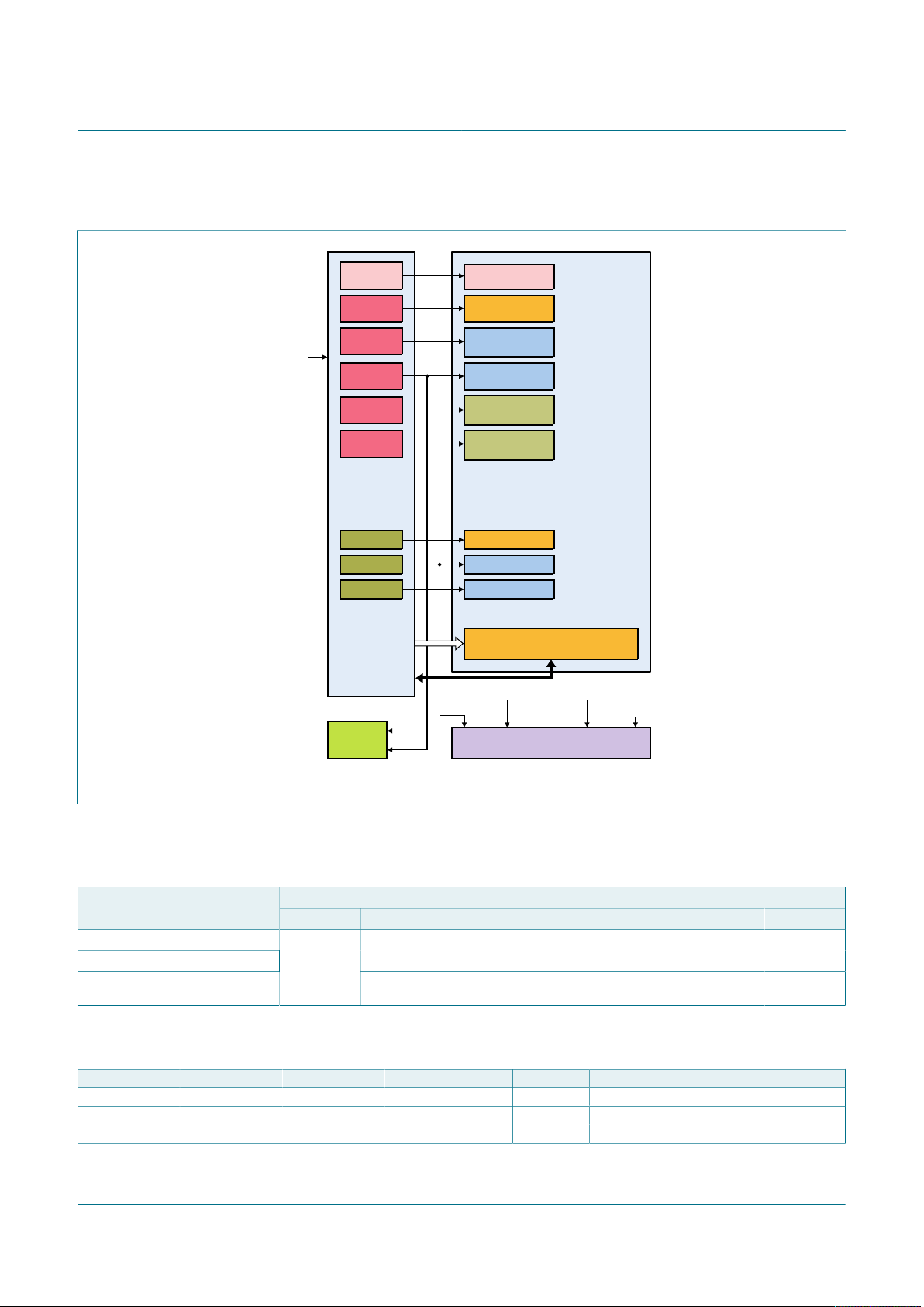
NXP Semiconductors
MCU
aaa- 029315
VDD_SNVS
VDD_DDRIO
VDD_MAIN
3.3 V I/O
(HV GPIO)
VDD_GPU
VDD_CPU(A35)
1.8 V I/O
(LV GPIO)
VDD_SCU
SDCARD0
2.5 V l/O
VIN:
2.7 V to
5.5 V
PF8101 / PF8201
VSNVS
BUCK7
BUCK6
BUCK5
BUCK2
BUCK1
LDO1
LDO2
LDO3
INTERFACING AND
I2C COMMUNICATIONS
Ethernet
eMMC SupplySIMCARD
SD Card
DRAM
CONTROL
SIGNALS
I2C
LPDDR
Memor y
MISCELLANEOUS
PERIPHERALS
9-channel power management integrated circuit for high performance applications
3 Simplified application diagram
PF8101; PF8201
Figure 1. Simplified application diagram
4 Ordering information
Table 1. Device options
PF8101 (automotive)
PF8201 (automotive)
PF8101 (industrial)
Table 2. Ordering information
Part number
MC33PF8101A0ES Automotive n/a Not programmed QM n/a
MC34PF8101A0EP Industrial n/a Not programmed QM n/a
MC33PF8201A0ES Automotive n/a Not programmed ASIL B n/a
[1] To order parts in tape and reel, add the R2 suffix to the part number.
PF8101_PF8201 All information provided in this document is subject to legal disclaimers. © NXP B.V. 2021. All rights reserved.
Product data sheet Rev. 4 — 24 February 2021
[1]
Target market NXP processor System comments Safety grade OTP ID
PackageType
Name Description Version
HVQFN56
HVQFN56, plastic, thermally enhanced very thin quad; flat non-leaded package,
wettable flanks; 56 terminals; 0.5 mm pitch; 8 mm x 8 mm x 0.85 mm body
HVQFN56, plastic, thermally enhanced very thin quad; flat non-leaded package,
56 terminals; 0.5 mm pitch; 8 mm x 8 mm x 0.85 mm body
SOT684-21
(DD/SC)
SOT684-21
2 / 126
Page 3

NXP Semiconductors
9-channel power management integrated circuit for high performance applications
5 Applications
• Automotive Infotainment
• High-end consumer and industrial
PF8101; PF8201
PF8101_PF8201 All information provided in this document is subject to legal disclaimers. © NXP B.V. 2021. All rights reserved.
Product data sheet Rev. 4 — 24 February 2021
3 / 126
Page 4
NXP Semiconductors
aaa-0 29316
EPAD
LDO3
LDO30 UT
LDO2EN
VSELECT
LDO3IN
SW5FB SW7IN SW7LX
Digita l Signal(s)
Analog Referenc e(s)
20 MHz Cl ock/Deriva tive
100 kHz Cl ock/Deriva tive
LDO2
LDO12IN
LDO2OUT
LDO2 VMO N
LDO3 VMO N
EA
AND
DRIVE R
SW7 MISC
REFEREN CE
SW7
VMON
LDO1
LDO1OUT
SYNCIN
SYNCOUT
AMUX
AGND
DGND
VIN
VSNVS
LICELL
V1P5D
VSNVS
VIN
OVLO
LDO1 VMO N
CLOCK MA NAGEMENT
(100 kHz / 20 MHz / PLL /
DIGITAL MO DULE)
24 CHAN NEL
ANALO G MUX
PMIC
INTERN AL
MONITO RS
PGOOD
MONITORS
SW1VMON
SW2VMO N
SW5VMO N
SW6VMON
SW7VMO N
LDO1VMON
LDO2V MON
LDO3V MON
EXTE RNAL
CHANN EL
INPUT
10 x DIE
TEMPER ATURE
MONITO RS
MANUA L TUNING
SPRE AD SPECTRUM
EXTER NAL CLOCK
SYNC
V1P5A
FSOBPGOOD
V
BG2
V
BG1
XFAILB
COIN CELL
CHARG ER
V1P5D
LDO
V1P5A
LDO
REGUL ATION
BANDG AP
BANDG AP
COMPAR ATOR
MONITOR ING
BANDG AP
FAIL SAFE
CONTRO L
EWARN BINTBRESETB MCU
WATCHDOG
TIMER
DIGITAL CO RE
AND
STATE MACHINE
THERMA L MONITORING
/ SHUTD OWN
OTP MEMO RY
WD monito ring
XINTTBBENSTANDBYPWRONWDISCLVDDIO VDDOTPSDA
V
BG2
V
BG2
V
BG2
V
BG2
EPAD
SW5FB
SW5IN
SW5LX
EA
AND
DRIVE R
REF
SELEC.
V
BG2
SW5
VMON
EPAD
SW6FB SW6IN SW6LX
EA
AND
DRIVE R
VTT
REFEREN CE
SELECTOR
SW6
VMON
REF
SELEC.
SW6 DVS
AND MI SC
REFEREN CE
SW5 DVS
AND MISC
REFEREN CE
÷ 2
V
BG2
EPAD
SW2FB
SW2IN
SW2LX
EA
AND
DRIVE R
REF
SELEC.
V
BG2
SW2
VMON
SW2 DVS
AND MISC
REFEREN CE
EPAD
SW1FB
SW1IN
SW1LX
EA
AND
DRIVE R
REF
SELEC.
V
BG2
SW1
VMON
SW1 DVS
AND MISC
REFEREN CE
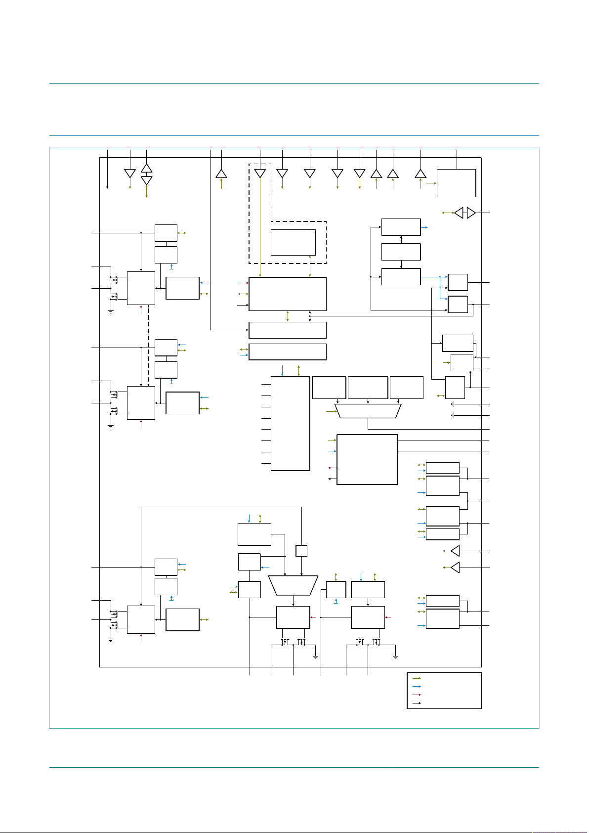
9-channel power management integrated circuit for high performance applications
6 Internal block diagram
PF8101; PF8201
Figure 2. Internal block diagram
PF8101_PF8201 All information provided in this document is subject to legal disclaimers. © NXP B.V. 2021. All rights reserved.
Product data sheet Rev. 4 — 24 February 2021
4 / 126
Page 5
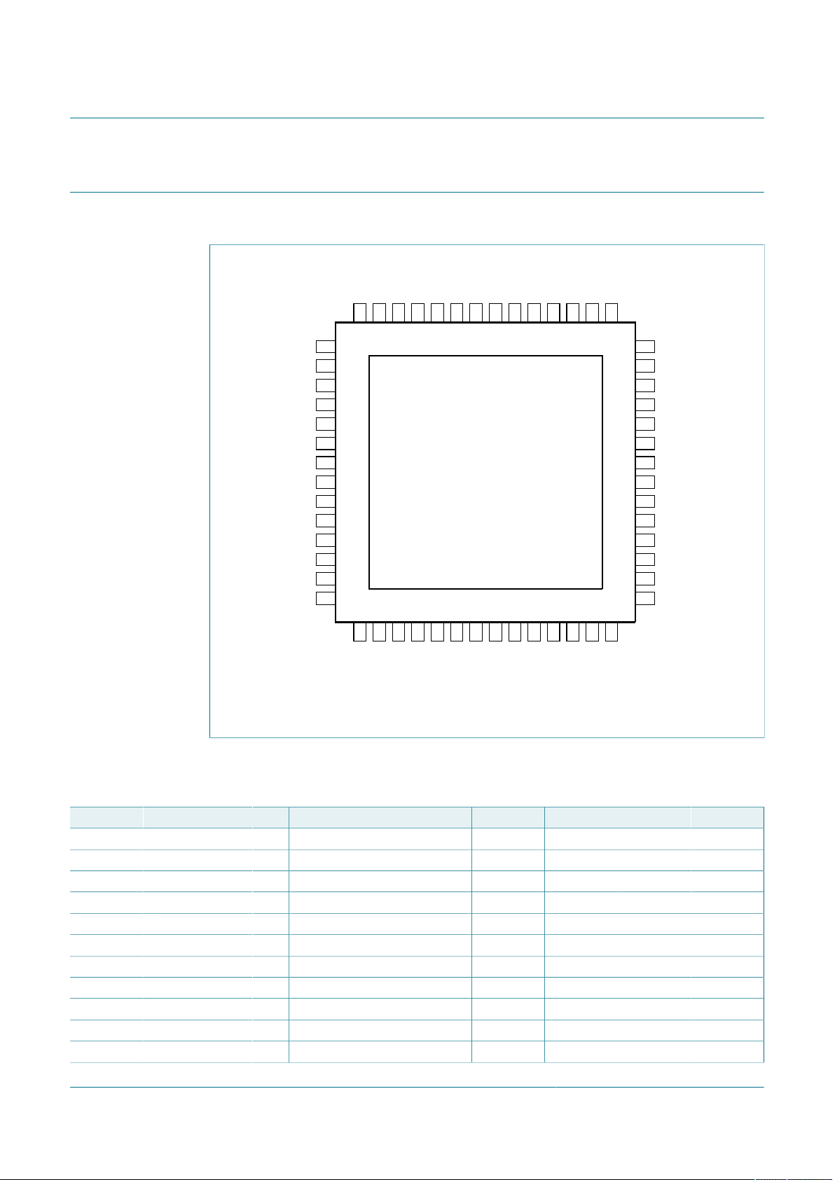
NXP Semiconductors
aaa- 029317
S
D
A
5
6
S
C
L
5
5
V
D
D
I
O
5
4
V
D
D
O
T
P
5
3
A
M
UX
52
A
G
N
D
5
1
V
I
N
5
0
S
Y
N
C
O
U
T
4
9
S
Y
N
C
I
N
4
8
V
S
N
V
S
47
L
I
C
E
L
L
4
6
D
G
ND
4
5
X
F
A
I
L
B
4
4
L
D
O
2
E
N
4
3
PGOOD
42
V1P5A
41
V1P5D
40
XINTB
39
SW7FB
38
SW7IN
37
SW7LX
36
SW6IN
35
SW6LX
34
SW5LX
33
SW5IN
32
SW5FB
31
SW6FB
30
FSOB
29
LDO1OUT
15
VSELECT
16
LDO12IN
17
LDO2OUT
18
WDI
19
EWARN
20
RESETB MCU
21
PWRON
22
STANDBY
23
INTB
24
LDO3OUT
25
LDO3IN
26
DNC8
27
DNC9
28
DNC1
1
SW2FB
2
SW1FB
3
SW1IN
4
SW1LX
5
SW2LX
6
SW2IN
EPAD
7
DNC2
8
DNC3
9
DNC4
10
DNC5
11
DNC6
12
DNC7
13
TBBEN
14
9-channel power management integrated circuit for high performance applications
7 Pinning information
7.1 Pinning
PF8101; PF8201
7.2 Pin description
Figure 3. Pin configuration for HVQFN56
Table 3. HVQFN56 pin description
Pin number Symbol Application description Pin type Min. Max. Units
1 DNC1 Do not connect — — — V
2 SW2FB Buck 2 output voltage feedback I −0.3 6.0 V
3 SW1FB Buck 1 feedback input I −0.3 6.0 V
4 SW1IN Buck 1 input supply I −0.3 6.0 V
5 SW1LX
6 SW2LX
7 SW2IN Buck 2 input supply I −0.3 6.0 V
8 DNC2 Do not connect — — — V
9 DNC3 Do not connect — — — V
10 DNC4 Do not connect — — — V
11 DNC5 Do not connect — — — V
PF8101_PF8201 All information provided in this document is subject to legal disclaimers. © NXP B.V. 2021. All rights reserved.
Product data sheet Rev. 4 — 24 February 2021
[1]
Buck 1 switching node O −0.3 6.0 V
[1]
Buck 2 switching node O −0.3 6.0 V
5 / 126
Page 6

NXP Semiconductors
PF8101; PF8201
9-channel power management integrated circuit for high performance applications
Pin number Symbol Application description Pin type Min. Max. Units
12 DNC6 Do not connect — — — V
13 DNC7 Do not connect — — — V
14 TBBEN Try Before Buy enable pin I −0.3 6.0 V
15 LDO1OUT LDO1 output O −0.3 6.0 V
16 VSELECT LDO2 voltage select input I −0.3 6.0 V
17 LDO12IN LDO1 and LDO2 input supply I −0.3 6.0 V
18 LDO2OUT LDO2 output O −0.3 6.0 V
19 WDI Watchdog Input from MCU I −0.3 6.0 V
20 EWARN Early warning to MCU O −0.3 6.0 V
21 RESETBMCU RESETBMCU open-drain output O −0.3 6.0 V
22 PWRON PWRON input I −0.3 6.0 V
23 STANDBY STANDBY input I −0.3 6.0 V
24 INTB INTB open-drain output O −0.3 6.0 V
25 LDO3OUT LDO3 output O −0.3 6.0 V
26 LDO3IN LDO3 input supply I −0.3 6.0 V
27 DNC8 Do not connect — — — V
28 DNC9 Do not connect — — — V
29 FSOB Safety output pin O −0.3 6.0 V
30 SW6FB Buck 6 output voltage feedback I −0.3 6.0 V
31 SW5FB Buck 5 output voltage feedback I −0.3 6.0 V
32 SW5IN Buck 5 input supply I −0.3 6.0 V
33 SW5LX
34 SW6LX
35 SW6IN Buck 6 input supply I -0.3 6.0 V
36 SW7LX
37 SW7IN Buck 7 input supply I −0.3 6.0 V
38 SW7FB Buck 7 output voltage feedback I −0.3 6.0 V
39 XINTB External interrupt input I −0.3 6.0 V
40 V1P5D 1.6 V digital core supply O −0.3 2.0 V
41 V1P5A 1.6 V analog core supply O −0.3 2.0 V
42 PGOOD PGOOD open-drain output O −0.3 6.0 V
43 LDO2EN LDO2 enable pin I −0.3 6.0 V
44 XFAILB External synchronization pin I/O -0.3 6.0 V
45 DGND Digital ground GND −0.3 0.3 V
46 LICELL Coin cell input I −0.3 5.5 V
47 VSNVS VSNVS regulator output O −0.3 6.0 V
48 SYNCIN External clock input pin for
49 SYNCOUT Clock out pin for external part
50 VIN Main input voltage to PMIC I −0.3 6.0 V
51 AGND Analog ground GND −0.3 0.3 V
[1]
Buck 5 switching node O −0.3 6.0 V
[1]
Buck 6 switching node O −0.3 6.0 V
[1]
Buck 7 switching node O −0.3 6.0 V
synchronization
synchronization
I −0.3 6.0 V
O −0.3 6.0 V
PF8101_PF8201 All information provided in this document is subject to legal disclaimers. © NXP B.V. 2021. All rights reserved.
Product data sheet Rev. 4 — 24 February 2021
6 / 126
Page 7

NXP Semiconductors
PF8101; PF8201
9-channel power management integrated circuit for high performance applications
Pin number Symbol Application description Pin type Min. Max. Units
52 AMUX Analog multiplexer output O −0.3 6.0 V
53 VDDOTP OTP selection input I −0.3 10 V
54 VDDIO I/O supply voltage. Connect to
voltage rail between 1.6 V and 3.3
V
55 SCL I2C clock signal I −0.3 6.0 V
56 SDA I2C data signal I/O −0.3 6.0 V
57 EPAD Exposed pad
Connect to ground
[1] Minimum voltage specification is given for DC voltage condition. While the regulator is switching, the LX pin may experience transient voltage spikes as
low as −3.0 V during the dead band time(<5 ns). The LX pins are tolerant to such transient spikes, however, it is responsibility of the hardware designer
to follow proper layout design guidelines to minimize the impact of parasitic inductance in the power path of the switching regulator, thus keeping the
magnitude of the negative voltage spike at the LX pin below 3.0 V.
I −0.3 6.0 V
GND −0.3 0.3 V
8 Absolute maximum ratings
Table 4. Absolute maximum ratings
Symbol Parameter Min Typ Max Unit
VIN Main input supply voltage
SWxVIN,
LDOxVIN
VDDOTP OTP programming input supply voltage −0.3 — 10 V
VLICELL Coin cell voltage −0.3 — 5.5 V
Regulator input supply voltage
[1]
−0.3 — 6.0 V
[1]
−0.3 — 6.0 V
[1] Pin reliability may be affected if system voltages are above the maximum operating range of 5.5 V for extended periods of time. To minimize system
reliability impact, system must not operate above 5.5 V for more than 1800 sec over the lifetime of the device.
9 ESD ratings
Table 5. ESD ratings
All ESD specifications are compliant with AEC-Q100 specification.
Symbol Parameter Min Typ Max Unit
V
ESD
V
ESD
I
LATCHUP
[1] ESD testing is performed in accordance with the human body model (HBM) (CZAP = 100 pF, RZAP = 1500 Ω), and the charge device model (CDM),
robotic (CZAP = 4.0 pF)
Human Body Model
Charge Device Model
QFN package - all pins
Latch-up current — — 100 mA
[1]
— — 2000 V
[1]
—
—
500
V
10 Thermal characteristics
Table 6. Thermal characteristics
Symbol Parameter Min Typ Max Unit
T
A
T
J
T
ST
Ambient operating temperature
Junction temperature −40 — 150 °C
Storage temperature range −55 — 150 °C
[1]
−40 — 105 °C
PF8101_PF8201 All information provided in this document is subject to legal disclaimers. © NXP B.V. 2021. All rights reserved.
Product data sheet Rev. 4 — 24 February 2021
7 / 126
Page 8

NXP Semiconductors
PF8101; PF8201
9-channel power management integrated circuit for high performance applications
Symbol Parameter Min Typ Max Unit
T
PPRT
[1] All parameters are specified up to a junction temperature of 150 °C. All parameters are tested at TA from −40°C to 105 °C to allow headroom for self
heating during operation. If higher TA operation is required, proper thermal and loading consideration must be made to ensure device operation below the
maximum TJ = 150 °C.
Table 7. QFN56 thermal resistance and package dissipation ratings
Symbol Parameter Min Max Unit
R
θJA
R
θJA
R
θJA
R
θJMA
R
θJMA
R
θJB
R
θJC
ΨJT Junction to package (top)
Peak package reflow temperature — — 260 °C
Junction to Ambient Natural Convection
[1] [2]
— 81 °C/W
Single Layer Board (1s)
Junction to Ambient Natural Convection
[1] [2]
— 27 °C/W
Four Layer Board (2s2p)
Junction to Ambient Natural Convection
— 22 °C/W
Eight Layer Board (2s6p)
Junction to Ambient (@200ft/min)
[1] [3]
— 66 °C/W
Single Layer Board (1s)
Junction to Ambient (@200ft/min)
[1] [3]
— 22 °C/W
Four Layer Board (2s2p)
Junction to Board
Junction to Case (bottom)
[4]
— 11 °C/W
[5]
— 0.6 °C/W
[6]
— 1 °C/W
[1] Junction temperature is a function of die size, on-chip power dissipation, package thermal resistance, mounting site (board) temperature, ambient
temperature, air flow, power dissipation of other components on the board, and board thermal resistance.
[2] Per JEDEC JESD51-2 with natural convection for horizontally oriented board. Board meets JESD51-9 specification for 1s or 2s2p board, respectively.
[3] Per JEDEC JESD51-6 with forced convection for horizontally oriented board. Board meets JESD51-9 specification for 1s or 2s2p board, respectively.
[4] Thermal resistance between the die and the printed circuit board per JEDEC JESD51-8. Board temperature is measured on the top surface of the board
near the package.
[5] Thermal resistance between the die and the solder pad on the bottom of the package. Interface resistance is ignored.
[6] Thermal characterization parameter indicating the temperature difference between package top and the junction temperature per JEDEC JESD51-2.
When Greek letters are not available, the thermal characterization parameter is written as Psi-JT.
11 Operating conditions
Table 8. Operating conditions
Symbol Parameter Min Typ Max Unit
V
IN
V
LICELL
Main input supply voltage UVDET — 5.5 V
LICELL input voltage range — — 4.2 V
12 General description
12.1 Features
The PF8101/PF8201 is a power management integrated circuit (PMIC) designed to be
the primary power management building block for NXP high-end multimedia application
processors from the i.MX 8 series. It is also capable of providing power solution to the
high end i.MX 6 series as well as several non-NXP processors.
• Buck regulators
– SW1, SW2, SW5, SW6: 0.4 V to 1.8 V; 2500 mA; up to 1.5 % accuracy
PF8101_PF8201 All information provided in this document is subject to legal disclaimers. © NXP B.V. 2021. All rights reserved.
Product data sheet Rev. 4 — 24 February 2021
8 / 126
Page 9

NXP Semiconductors
9-channel power management integrated circuit for high performance applications
– SW7; 1.0 V to 4.1 V; 2500 mA; 2 % accuracy
– Dynamic voltage scaling on SW1, SW2, SW5, SW6
– SW1, SW2 configurable as a dual phase regulator
– SW5, SW6 configurable as a dual phase regulator
– VTT termination mode on SW6
– Programmable current limit
– Spread-spectrum and manual tuning of switching frequency
• LDO regulators
– LDO1, 1.5 V to 5.0 V, 400 mA: 3 % accuracy with optional load switch mode
– LDO2, 1.5 V to 5.0 V, 400 mA; 3 % accuracy with optional load switch mode and
– LDO3, 1.5 V to 5.0 V, 400 mA; 3 % accuracy with optional load switch mode
• RTC LDO/Switch supply from system supply or coin cell
– RTC supply VSNVS 1.8 V/3.0 V/3.3 V, 10 mA
– Battery backed memory including coin cell charger with programmable charge
• System features
– Fast PMIC startup
– Advanced state machine for seamless processor interface
– High speed I2C interface support (up to 3.4 MHz)
– PGOOD monitor
– User programmable standby and off modes
– Programmable soft start sequence and power down sequence
– Programmable regulator configuration
– 24 channel analog multiplexer for smart system monitoring/diagnostic
• OTP (One time programmable) memory for device configuration
• Monitoring circuit to fit ASIL B safety level
– Independent voltage monitoring with programmable fault protection
– Advance thermal monitoring and protection
– External watchdog monitoring and programmable internal watchdog counter
– I2C CRC and write protection mechanism
– Analog built-in self-test (ABIST)
PF8101; PF8201
selectable hardware/software control
current and voltage
PF8101_PF8201 All information provided in this document is subject to legal disclaimers. © NXP B.V. 2021. All rights reserved.
Product data sheet Rev. 4 — 24 February 2021
9 / 126
Page 10
NXP Semiconductors
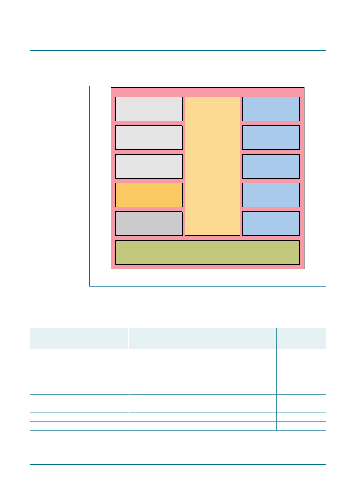
aaa- 029318
PF8101 / PF8201 FUNCTIONAL BLOCK DIAGR AM
LDO1
(1.5 V TO 5 V, 400 mA)
VSNVS (RTC SUPPLY)
(1.8 V/3.0 V/3.3 V, 10 mA)
LDO2
(1.5 V TO 5 V, 400 mA)
LOGIC AND CONTROL
I2C
WATCHDOG
MCU INTERFACE
REGUL ATOR CONTRO L
FAULT DETECTION
FUNCTIONAL SAFETY
(ABIST )
LDO3
(1.5 V TO 5 V, 400 mA)
24 CHANNEL AMUX
(DIAGNOSTICS)
OTP
(FLEXIBLE CONFIGUR ATION)
BUCK1 (MASTER /SL AVE)
(0.4 V TO 1.8 V, 2.5 A)
BUCK2 (MASTER /SLAVE)
(0.4 V TO 1.8 V, 2.5 A)
BUCK5 (MASTER/SLAVE)
(0.4 V TO 1.8 V, 2.5 A)
BUCK6 (MASTER/SLAVE)
(VT T/0.4 V TO 1.8 V, 2.5 A)
BUCK7 (INDEPENDENT)
(1.0 V TO 4.1 V, 2.5 A)
9-channel power management integrated circuit for high performance applications
12.2 Functional block diagram
PF8101; PF8201
Figure 4. Functional block diagram
12.3 Power tree summary
The following table shows a summary of the voltage regulators in the PF8101/PF8201.
Table 9. Voltage supply summary
Regulator Type Input supply Regulated output
SW1 Buck SW1IN 0.4 V to 1.8 V 6.25 2500
SW2 Buck SW2IN 0.4 V to 1.8 V 6.25 2500
SW5 Buck SW5IN 0.4 V to 1.8 V 6.25 2500
SW6 Buck SW6IN VTT/0.4 V to 1.8 V 6.25 2500
SW7 Buck SW7IN 1.0 V to 4.1 V — 2500
LDO1 Linear (P-type) LDO12IN 1.5 V to 5.0 V — 400
LDO2 Linear (P-type) LDO12IN 1.5 V to 5.0 V — 400
LDO3 Linear (P-type) LDO3IN 1.5 V to 5.0 V — 400
VSNVS LDO/Switch VIN/LICELL 1.8 V/3.0 V/3.3 V — 10
PF8101_PF8201 All information provided in this document is subject to legal disclaimers. © NXP B.V. 2021. All rights reserved.
Product data sheet Rev. 4 — 24 February 2021
range (V)
VOUT
programmable step
(mV)
IRATED (mA)
10 / 126
Page 11

NXP Semiconductors
PF8101; PF8201
9-channel power management integrated circuit for high performance applications
12.4 Device differences
Table 10. Device differences
Description PF8201 PF8101 Bits not available on PF8101
During the self-test, the device checks:
• The high speed oscillator circuit is operating within
a maximum of 15 % tolerance
• A CRC is performed on the mirror registers during
the self-test routine to ensure the integrity of the
registers before powering up
• ABIST test on all voltage monitors and toggling
signals
Fail-safe state: to lock down the system in case of
critical failures cycling the PMIC on/off
ABIST on demand Available Not available AB_RUN
Active safe state: allow the FSOB to remain asserted
as long as any of the non-safe conditions are present.
Allow the system to be set in safe state via the FSOB
pin.
Secure I2C write: I2C write procedure to modify
registers dedicated to safety features (I2C CRC is still
available)
Available Not available AB_SWx_OV
AB_SWx_UV
AB_LDOx_OVAB_LDOx_UV
STEST_NOK
Available Not available FS_CNT[3:0]
OTP_FS_BYPASS
OTP_FS_MAX_CNT[3:0]
OTP_FS_OK_TIMER[2:0]
Available Not available FSOB_ASS_NOK
OTP_FSOB_ASS_EN (always 0)
Available Not available I2C_SECURE_EN
OTP_I2C_SECURE _EN (always 0)
RANDOM_GEN[7:0]
RANDOM_CHK[7:0]
PF8101_PF8201 All information provided in this document is subject to legal disclaimers. © NXP B.V. 2021. All rights reserved.
Product data sheet Rev. 4 — 24 February 2021
11 / 126
Page 12
NXP Semiconductors
aaa-029376
Fault
WD_Reset
D
Q
O
L
R
F
K
U
J
P
M
C
E
Z
N
S
Fault
POWER DOWN
Turn-Off
POWER DOWN
1. WD_FAIL_CNT = WD_MAX_CNT
OR
2. PU_FAIL = True
OR
3. FAULT_CNT = FAULT_MAX_CNT
OR
4. Fault_Timer_Expired
OR
5. Tj > TSD
1. PWRON = 0
OR
2. PWRON H to L &&
PWRON = 0 > TRESET
OR
3. PMIC_OFF = 1 &&
500us_Shutdown_timer_expired
OR
4. VIN_OVLO_SDWN = 1 &&
VIN_OVLO detected
5. XFAILB H to L &&
20us Sync time expired.
(Only if OTP_XFAILB_EN = 1)
* Output is enabled/asserted if it is programmed to do so by the OTP configuration
Turn-off
Power Up
Sequence
Off Modes
Hard WD Reset
Event
System ON
Power up regulators
per OTP sequence
PU_FAIL = True
Power up
failure
BG_OK
OTP_OK
20 MHz_OK
FS_CNT++
Regulators off
VSNVS = On*
FSOB = LOW*
Fail self-test
(ST_COUNT < 3)
FS_CNT = FS_MAX_CNT
&& OTP_FS_BYPASS = 0
1. FS_CNT < FS_MAX_CNT
OR
2. OTP_FS_BYPASS = 1
Regulators off
FSOB = LOW*
VSNVS = On*
TRIM_NOK = 0
&& OTP_NOK = 0
&& STEST_NOK = 0
VIN > UVDET
V1P5D_POR
V1P5A_POR
VIN < UVDET
CRITICAL FAILURE
WD_FAIL_CNT++
RESETBMCU = HIGH
Sys ON
Sequence
RUN
F
a
u
l
t
S
h
u
t
d
o
w
n
F
a
i
l
s
e
l
f
-
t
e
s
t
s
(
S
T
_
C
O
U
N
T
=
3
)
T
u
r
n
-
o
f
f
e
v
e
n
t
Standby
B
A
QPU_Off
LP_Off
Self-
Test
2 ms
delay
OTP &
Trim Load
VSNVS On*
Fail-Safe
State
Fail-Safe
Transition
Power Down
NO
POWER
PF8201 only
PF8101 only
9-channel power management integrated circuit for high performance applications
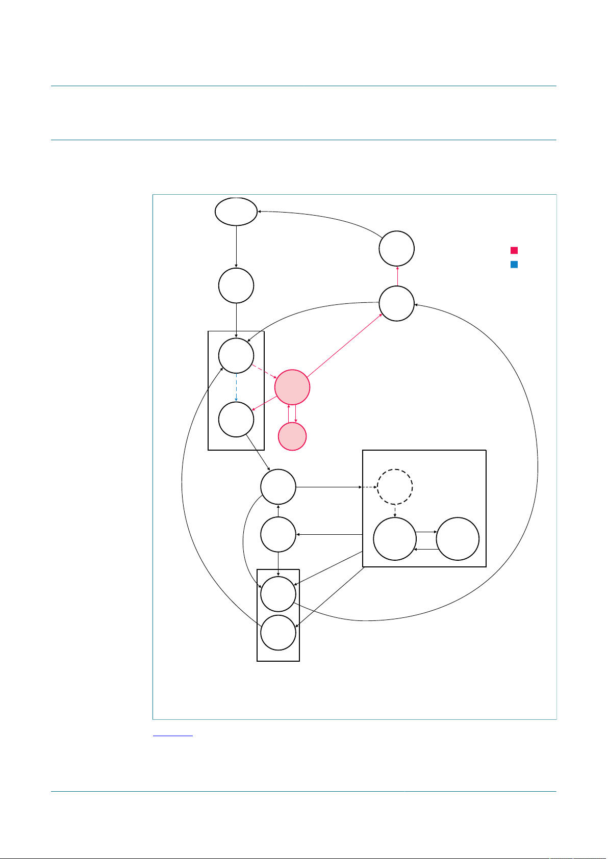
13 State machine
The PF8101/PF8201 features a state of the art state machine for seamless processor
interface. The state machine handles the IC start up, provides fault monitoring and
reporting, and protects the IC and the system during fault conditions.
PF8101; PF8201
PF8101_PF8201 All information provided in this document is subject to legal disclaimers. © NXP B.V. 2021. All rights reserved.
Product data sheet Rev. 4 — 24 February 2021
Figure 5. State diagram
Table 11 lists the conditions for the different state machine transitions.
12 / 126
Page 13

NXP Semiconductors
PF8101; PF8201
9-channel power management integrated circuit for high performance applications
Table 11. State machine transition definition
Symbol Description Conditions
Transition A Standby to run
Transition B Run to standby
Transition C System on to WD reset 1. Hard WD Reset event
Transition D WD reset to system on 1. 30 µs delay passed && WD_EVENT_CNT < WD_MAX_CNT
Transition E WD reset to power down (fault) 1. WD_EVENT_CNT = WD_MAX_CNT
Transition J LP_Off to self-test (PF8201 only)
Transition K Self-test to QPU_Off (PF8201 only)
Transition F LP_Off to QPU_Off (PF8101 only)
1. STANDBY = 0 && STANDBYINV bit = 0
2. STANDBY = 1 && STANDBYINV bit = 1
1. STANDBY = 1 && STANDBYINV bit = 0
2. STANDBY = 0 && STANDBYINV bit = 1
Transitory off state: device pass through LP_Off to Self-Test to QPU_
Off (no power up event present)
1. LPM_OFF = 1 && TBBEN = Low
Power up event from LP_Off state
2. LPM_OFF = 0
&& TBBEN = Low
&& (PWRON = 1 && OTP_PWRON_MODE = 0)
&& UVDET< VIN < VIN_OVLO (or VIN_OVLO disabled)
&& TJ < T
&& TRIM_NOK = 0 && OTP_NOK = 0
Power up event from LP_Off state
3. LPM_OFF = 0
&& TBBEN = Low
&& (PWRON H to L && OTP_PWRON_MODE = 1
&& UVDET < VIN < VIN_OVLO (or VIN_OVLO disabled)
&& TJ < T
&& TRIM_NOK = 0 && OTP_NOK = 0
Conditions: Transitory Off state to go into TBB Mode. Device pass
through LP_Off to Self-Test to QPU_Off (no power up event present)
4. TBBEN = high (V1P5D)
1. Pass Self-Tests
2. TBBEN = high (V1P5D)
Transitory Off state: device pass through LP_Off to QPU_Off (no
power up event present)
1. LPM_OFF = 1
&& TBBEN = Low
Power up event from LP_Off state
2. LPM_OFF = 0
&& TBBEN = Low
&& (PWRON = 1 && OTP_PWRON_MODE = 0)
&& UVDET< VIN < VIN_OVLO (or VIN_OVLO disabled)
&& TJ < T
&& TRIM_NOK = 0 && OTP_NOK = 0
Power up event from LP_Off state
3. LPM_OFF = 0
&& TBBEN = Low
&& (PWRON H to L && OTP_PWRON_MODE = 1)
&& UVDET < VIN < VIN_OVLO (or VIN_OVLO disabled)
&& TJ < TSD && TRIM_NOK = 0 && OTP_NOK = 0
Transitory Off state: device pass through LP_Off to QPU_Off (no
power up event present)
4. TBBEN = High (V1P5D)
SD
SD
SD
PF8101_PF8201 All information provided in this document is subject to legal disclaimers. © NXP B.V. 2021. All rights reserved.
Product data sheet Rev. 4 — 24 February 2021
13 / 126
Page 14

NXP Semiconductors
9-channel power management integrated circuit for high performance applications
Symbol Description Conditions
Transitory QPU_Off state, power on event occurs from LP_Off state,
after self-test is passed, QPU_Off is just a transitory state until power
up sequence starts.
1. LPM_OFF = 0
&& TBBEN = Low
&& TRIM_NOK = 0 && OTP_NOK = 0 && STEST_NOK=0
Power up event from QPU_Off state
2. LPM_OFF = 1
&& (PWRON = 1 && OTP_PWRON_MODE = 0)
&& UVDET < VIN < VIN_OVLO (or VIN_OVLO disabled
&& TJ < T
&& TRIM_NOK = 0 && OTP_NOK = 0 && STEST_NOK = 0
Power up event from QPU_Off state
3. LPM_OFF = 1
&& (PWRON H to L && OTP_PWRON_MODE = 1)
&& UVDET < VIN < VIN_OVLO (or VIN_OVLO disabled)
&& TJ < T
&& TRIM_NOK = 0 && OTP_NOK = 0 && STEST_NOK = 0
Power up event from QPU_Off state
4. TBBEN = High
&& (PWRON = 1 && OTP_PWRON_MODE = 0)
&& UVDET < VIN < VIN_OVLO (or VIN_OVLO disabled
J < T
&& T
&& TRIM_NOK = 0 && OTP_NOK = 0 && STEST_NOK = 0
Transition L QPU_Off to power up
Power up event from QPU_Off state
5. TBBEN = High
&& (PWRON H to L && OTP_PWRON_MODE = 1)
&& UVDET < VIN < VIN_OVLO (or VIN_OVLO disabled)
&& TJ < T
&& TRIM_NOK = 0 && OTP_NOK = 0 && STEST_NOK = 0
Transitory QPU_Off state, Power on event occurs from LP_Off state,
after self-test is passed, QPU_Off is just a transitory state until power
up sequence starts
6. LPM_OFF = 0
&& TBBEN = Low
&& TRIM_NOK = 0 && OTP_NOK = 0 && STEST_NOK = 0
&& OTP_XFAILB_EN = 1 && XFAILB = HIGH
Power up event from QPU_Off state
7. LPM_OFF = 1
&& (PWRON = 1 && OTP_PWRON_MODE = 0)
&& TJ < T
&& UVDET < VIN < VIN_OVLO (or VIN_OVLO disabled
&& TRIM_NOK = 0 && OTP_NOK = 0 && STEST_NOK = 0
&& OTP_XFAILB_EN = 1 && XFAILB = HIGH
Power up event from QPU_Off state
8. LPM_OFF = 1
&& (PWRON H to L && OTP_PWRON_MODE = 1)
&& TJ < T
&& UVDET < VIN < VIN_OVLO (or VIN_OVLO disabled)
&& TRIM_NOK = 0 && OTP_NOK = 0 && STEST_NOK = 0
&& OTP_XFAILB_EN = 1 && XFAILB = HIGH
PF8101; PF8201
SD
SD
SD
SD
SD
SD
PF8101_PF8201 All information provided in this document is subject to legal disclaimers. © NXP B.V. 2021. All rights reserved.
Product data sheet Rev. 4 — 24 February 2021
14 / 126
Page 15

NXP Semiconductors
PF8101; PF8201
9-channel power management integrated circuit for high performance applications
Symbol Description Conditions
Power up event from QPU_Off state during TBB mode
9. TBBEN =1
&& (PWRON = 1 && OTP_PWRON_MODE = 0)
&& TJ < T
&& UVDET < VIN < VIN_OVLO (or VIN_OVLO disabled)
&& TRIM_NOK = 0 && OTP_NOK = 0 && STEST_NOK = 0
&& OTP_XFAILB_EN = 1 && XFAILB = HIGH
Power up event from QPU_Off state during TBB mode
10. TBBEN = 1
&& (PWRON H to L && OTP_PWRON_MODE = 1)
&& TJ < T
&& UVDET < VIN < VIN_OVLO (or VIN_OVLO disabled)
&& TRIM_NOK = 0 && OTP_NOK = 0 && STEST_NOK = 0
&& OTP_XFAILB_EN = 1 && XFAILB = HIGH
Transition M Power up sequence to system on 1. RESETBMCU is released as part of the power up sequence
Requested turn off event
1. OTP_PWRON_MODE = 0 && PWRON = 0
Requested turn off event
2. OTP_PWRON_MODE = 1 && (PWRON H to L && PWRON = low
for t > TRESET)
Requested turn off event
Transition N System on to power down (turn off)
Transition Z System on to power down (fault)
Transition O Power down (turn off) to LP_Off Requested turn off event moves directly to LP_Off
Transition Q Power up to power down (fault) Power up failure
Transition R Self-test to fail-safe transition 1. Self-tests fail 3 times
Transition S Power down (fault) to fail-safe transition Turn off event due to a fault condition moves to fail-safe transition
Transition U Fail-safe transition to LP_Off
Transition P Fail-safe transition to fail-safe state
(PF8201 only)
3. PMIC_OFF = 1 && 500µs_Shutdown_Timer_Expired
Protective turn off event (no PMIC fault)
4. VIN_OVLO_SDWN=1 && VIN_OVLO detected for longer than VIN_
OVLO_DBNC time
External turn off event (no PMIC fault)
5. OTP_XFAILB_EN = 1
&& XFAILB → Low && 20 µs synchronization time is expired
Turn off event due to PMIC fault
1. Fault Timer expired
Turn off event due to PMIC fault
2. FAULT_CNT = FAULT_MAX_CNT
Turn off event due to PMIC fault
3. Thermal shutdown TJ > T
1. Power down sequences finished
1. Failure during power up sequence
&& TBBEN = low
1. Power down sequence is finished
1. FS_CNT < FS_MAX_CNT
2. OTP_FS_BYPASS = 1
1. FS_CNT = FS_MAX_CNT
&& OTP_FS_BYPASS = 0
SD
SD
SD
13.1 States description
13.1.1 OTP/TRIM load
Upon VIN application V1P5D and V1P5A regulators are turned on automatically. Once
the V1P5D and V1P5A cross their respective POR thresholds, the fuses (for trim and
OTP) are loaded into the mirror registers and into the functional I2C registers if configured
by the voltage on the VDDOTP pin.
PF8101_PF8201 All information provided in this document is subject to legal disclaimers. © NXP B.V. 2021. All rights reserved.
Product data sheet Rev. 4 — 24 February 2021
15 / 126
Page 16

NXP Semiconductors
9-channel power management integrated circuit for high performance applications
The fuse circuits have a CRC error check routine which reports and protects against
register loading errors on the mirror registers. If a register loading error is detected, the
corresponding TRIM_NOK or OTP_NOK flag is asserted. See Section 17 "OTP/TBB and
default configurations" for details on handling fuse load errors.
If no fuse load errors are present, VSNVS is configured as indicated in the OTP
configuration bits, and the state machine moves to the LP_OFF state.
13.1.2 LP_Off state
The LP_Off state is a low power off mode selectable by the LPM_OFF bit during
the system on modes. By default, the LPM_OFF = 0 when VIN crosses the UVDET
threshold, therefore the state machine stops at the LP_Off state until a valid power up
event is present. When LPM_OFF= 1, the state machine transitions automatically to the
QPU_Off state if no power up event has been present and waits in the QPU_Off until a
valid power up event is present.
The selection of the LPM_OFF bit is based on whether prioritizing low quiescent current
(stay in LP_Off) or quick power up (move to QPU_Off state).
If a power up event is started in LP_Off state with LPM_OFF = 0 and a fuse loading error
is detected, the PF8101/PF8201 ignores the power up event and remains in the LP_Off
state to avoid any potential damage to the system.
PF8101; PF8201
To be in LP_Off state, it is necessary to have VIN present. If a valid LICELL is present,
but VIN is below the UVDET, the PF8101/PF8201 enters the coin cell state.
13.1.3 Self-test routine (PF8201 only)
When device transitions from the LP_Off state, it turns on all necessary internal circuits
as it moves into the self-test routine and performs a self-check routine to verify the
integrity of the internal circuits.
During the self-test routine the following blocks are verified:
• The high speed clock circuit is operating within a maximum of 15 % tolerance
• The output of the voltage generation bandgap and the monitoring bandgap are not
more than 4 % to 12 % apart from each other
• A CRC is performed on the mirror registers during the self-test routine, to ensure the
integrity of the registers before powering up
• ABIST test on all voltage monitors.
To allow for varying settling times for the internal bandgap and clocks, the self-test block
is executed up to 3 times (with 2.0 ms between each test) if a failure is encountered, the
state machine proceeds to the fail-safe transition.
A failure in the ABIST test is not interpreted as a self-test failure and it only sets the
corresponding ABIST flag for system information. The MCU is responsible for reading the
information and deciding whether it can continue with a safe operation. See Section 18.1
"System safety strategy" for more information about the functional safety strategy of
PF8201.
Upon a successful self-test, the state machine proceeds to the QPU_Off state.
PF8101_PF8201 All information provided in this document is subject to legal disclaimers. © NXP B.V. 2021. All rights reserved.
Product data sheet Rev. 4 — 24 February 2021
16 / 126
Page 17

NXP Semiconductors
9-channel power management integrated circuit for high performance applications
13.1.4 QPU_Off state
The QPU_Off state is a higher power consumption off mode, in which all internal circuitry
required for a power on is biased and ready to start a power up sequence.
If LPM_OFF = 1 and no turn on event is present, the device stops at the QPU_Off state,
and waits until a valid turn on event is present.
In this state, if VDDIO supply is provided externally, the device is able to communicate
through I2C to access and modify the mirror registers in order to operate the device in
TBB mode or to program the OTP registers as described in Section 17 "OTP/TBB and
default configurations".
By default, the coin cell charger is disabled during the QPU_Off state when VIN crosses
the UVDET threshold, but it may be turned on or off in this state once it is programmed
by COINCHG_OFF during the system-on states.
If a power up event is started and any of the TRIM_NOK, OTP_NOK or STEST_NOK
flags are asserted, the device ignores the power up event and remains in the QPU_Off
state. See Section 17 "OTP/TBB and default configurations" for more details on
debugging a fuse loading failure.
Upon a power up event, the default configuration from OTP or hardwire is loaded into
their corresponding I2C functional register in the transition from QPU_Off to power up
state.
PF8101; PF8201
13.1.5 Power up sequence
During the power up sequence, the external regulators are turned on in a predefined
order as programmed by the default (OTP or hardwire) sequence.
If PGOOD is used as a GPO, it can also be set high as part of the power up sequence in
order to allow sequencing of any external supply/device controlled by the PGOOD pin.
The RESETBMCU is also programmed as part of the power up sequence, and it is used
as the condition to enter system-on states. The RESETBMCU may be released in the
middle of the power up sequence, in this case, the remaining supplies in the power up
continues to power up as the device is in the run state. See Section 14.5.2 "Power up
sequencing" for details.
13.1.6 System-on states
During the system-on states, the MCU is powered and out of reset and the system is fully
operational.
The system on is a virtual state composed by two modes of operations:
• Run state
• Standby state
Register to control the regulators output voltage, regulator enable, interrupt masks, and
other miscellaneous functions can be written to or read from the functional I2C register
map during the system-on states.
13.1.6.1 Run state
If the power up state is successfully completed, the state machine transitions to the run
state. In this state, RESETBMCU is released high, and the MCU is expected to boot up
and set up specific registers on the PMIC as required during the system boot up process.
PF8101_PF8201 All information provided in this document is subject to legal disclaimers. © NXP B.V. 2021. All rights reserved.
Product data sheet Rev. 4 — 24 February 2021
17 / 126
Page 18

NXP Semiconductors
9-channel power management integrated circuit for high performance applications
The run mode is intended to be used as the normal mode of operation for the system.
Each regulator has specific registers to control its output voltage, operation mode and/or
enable/disable state during the run state.
By default, the VSWx_RUN[7:0] / VLDOx_RUN[3:0] registers are loaded with the data
stored in the OTP_VSWx[7:0] or OTP_VLDOx[3:0] bits respectively.
SW7 uses only one global register to configure the output voltage during run or
standby mode. Upon power up the VSW7[4:0] bits are loaded with the values of the
OTP_VSW7[4:0].
Upon power up, if the switching regulator is part of the power up sequence, the
SWx_RUN_MODE[1:0] bits will be loaded as needed by the system:
• When OTP_SYNCIN_EN = 1, default SWx_RUN_MODE at power up is always set to
PWM (0b01)
• When OTP_SYNCOUT_EN = 1, default SWx_RUN_MODE at power up is always set
to PWM (0b01)
• When OTP_FSS_EN = 1, default SWx_RUN_MODE at power up shall always set to
PWM (0b01)
• If none of the above conditions are met, the default value of the SWx_RUN_MODE bits
at power up will be set by the OTP_SW_MODE bits.
PF8101; PF8201
When OTP_SW_MODE = 0, the default value of the SWx_RUN_MODE bits are set to
0b11 (autoskip).
When OTP_SW_MODE = 1, the default value of the SWx_RUN_MODE bits are set to
0b01 (PWM).
If the switching regulator is not part of the power up sequence, the
SWx_RUN_MODE[1:0] bits are loaded with 0b00 (OFF mode).
Likewise, if the LDO is part of the power up sequence, the LDOx_RUN_EN bit is set to
1 (enabled) by default. If the LDO is not selected as part of the power up sequence, the
LDOx_RUN_EN bit is set to 0 (disabled) by default.
In a typical system, each time the processor boots up (PMIC transitions from off mode
to run state), all output voltage configurations are reset to the default OTP configuration,
and the MCU should configure the PMIC to its desired usage in the application.
13.1.6.2 Standby state
The standby state is intended to be used as a low power (state retention) mode of
operation. In this state, the voltage regulators can be preset to a specific low power
configuration in order to reduce the power consumption during system’s sleep or state
retention modes of operations.
The standby state is entered when the STANDBY pin is pulled high or low as defined
by the STANBYINV bit. The STANDBY pin is pulled high/low by the MCU to enter/exit
system low power mode. See Section 14.9.2 "STANDBY" for detailed configuration of the
STANDBY pin.
Each regulator has specific registers to control its output voltage, operation mode and/or
enable/disable state during the standby state.
By default, the VSWx_STBY[7:0] / VLDOx_STBY[3:0] registers are loaded with the data
stored in the OTP_VSWx[7:0] or OTP_VLDOx[3:0] bits respectively.
PF8101_PF8201 All information provided in this document is subject to legal disclaimers. © NXP B.V. 2021. All rights reserved.
Product data sheet Rev. 4 — 24 February 2021
18 / 126
Page 19

NXP Semiconductors
9-channel power management integrated circuit for high performance applications
Upon power up, if the switching regulator is part of the power up sequence, the
SWx_STBY_MODE[1:0] bits will be loaded as needed by the system:
• When OTP_SYNCIN_EN = 1, default SWx_STBY_MODE at power up is always set to
PWM (0b01)
• When OTP_SYNCOUT_EN = 1, default SWx_STBY_MODE at power up is always set
to PWM (0b01)
• When OTP_FSS_EN = 1, default SWx_STBY_MODE at power up shall always set to
PWM (0b01)
• If none of the conditions above are met, the default value of the SWx_STBY_MODE
bits at power up will be set by the OTP_SW_MODE bits.
When OTP_SW_MODE = 0, the default value of the SWx_STBY_MODE bits are set to
0b11 (autoskip).
When OTP_SW_MODE = 1, the default value of the SWx_STBY_MODE bits are set to
0b01 (PWM).
If the switching regulator is not part of the power up sequence, the
SWx_STBY_MODE[1:0] bits are loaded with 0b00 (OFF mode).
Likewise, if the LDO is part of the power up sequence, the LDOx_RUN_EN bit is set to
1 (enabled) by default. If the LDO is not selected as part of the power up sequence, the
LDOx_RUN_EN bit is set to 0 (disabled) by default.
PF8101; PF8201
Upon power up, the standby registers are loaded with the same default OTP values as
the run mode. The MCU is expected to program the desired standby values during boot
up.
If any of the external regulators are disabled in the standby state, the power down
sequencer is engaged as described in Section 14.6.2 "Power down sequencing".
13.1.7 WD_Reset
When a hard watchdog reset is present, the state machine increments the
WD_EVENT_CNT[3:0] register and compares against the WD_MAX_CNT[3:0] register.
If WD_EVENT_CNT[3:0] = WD_MAX_CNT[3:0], the state machine detects a cyclic
watchdog failure, it powers down the external regulators and proceeds to the fail-safe
transition.
If WD_EVENT_CNT[3:0] < WD_MAX_CNT[3:0], the state machine performs a hard WD
reset.
A hard WD reset can be generated from either a transition in the WDI pin or a WD event
initiated by the internal watchdog counter as described in Section 15.11.2 "Watchdog
reset behaviors".
13.1.8 Power down state
During power down state, all regulators except VSNVS are disabled as configured in
the power down sequence. The power down sequence is programmable as defined in
Section 14.6.2 "Power down sequencing".
Two types of events may lead to the power down sequence:
• Non faulty turn off events: move directly into LP_Off state as soon as power down
sequence is finalized
PF8101_PF8201 All information provided in this document is subject to legal disclaimers. © NXP B.V. 2021. All rights reserved.
Product data sheet Rev. 4 — 24 February 2021
19 / 126
Page 20

NXP Semiconductors
9-channel power management integrated circuit for high performance applications
• Turn off events due to a PMIC fault: move to the fail-safe transition as soon as the
power down sequence is finalized
13.1.9 Fail-safe transition
The fail-safe transition is entered if the PF8101/PF8201 initiates a turn off event due to a
PMIC fault.
If the fail-safe transition is entered, the PF8101/PF8201 provides four FAIL bits to
indicate the source of the failure:
• The PU_FAIL is set to 1 when the device shuts down due to a power up failure
• The WD_FAIL is set to 1 when the device shuts down due to a watchdog event counter
max out
• The REG_FAIL is set to 1 when the device shuts down due to a regulator failure (fault
counter maxed out or fault timer expired)
• The TSD_FAIL is set to 1 when the device shuts down due to a thermal shutdown
The value of the FAIL bits is retained as long as VIN > UVDET.
The MCU can read the FAIL bits during the system-on states in order to obtain
information about the previous failure and can clear them by writing a 1 to them, provided
the state machine is able to power up successfully after such failure.
PF8101; PF8201
In PF8201, when the state machine enters the fail-safe transition, a fail-safe counter is
compared and increased, if the FS_CNT[3:0] reaches the maximum count, the device
can be programmed to move directly to the fail-safe state to prevent a cyclic failure from
happening.
13.1.10 Fail-safe state (PF8201 only)
The fail-safe state works as a safety lock-down upon a critical device/system failure. It is
reached when the FS_CNT [3:0] = FS_MAX_CNT [3:0].
A bit is provided to enable or disable the device to enter the fail-safe state upon a cyclic
failure. When the OTP_FS_BYPASS = 1, the fail-safe bypass operation is enabled and
the device always move to the LP_Off state, regardless of the value of the FS_CNT[3:0].
If the OTP_FS_BYPASS = 0, the fail-safe bypass is disabled, and the device moves to
the fail-safe state when the proper condition is met.
The maximum number of times the device can pass through the fail-safe
transition continuously prior to moving to a fail state is programmed by the
OTP_FS_MAX_CNT[3:0] bits. If the FS_MAX_CNT[3:0] = 0x00, the device moves into
the fail-safe state as soon as it fails for the very first time.
If the FSOB pin is programmed to assert upon a specific fault, the FSOB pin remains
asserted low during the fail-safe state if the corresponding fault is present when PF8201
reaches the fail-safe state.
The device can exit the fail-safe state only after a power cycle (VIN crossing UVDET)
event is present.
To avoid reaching the fail-safe state due to isolated fail-safe transition events,
the FS_CNT [3:0] is gradually decreased based on a fail-safe OK timer. The
OTP_FS_OK_TIME[2:0] bits select the default time configuration for the fail-safe OK
timer between 1 to 60 min.
PF8101_PF8201 All information provided in this document is subject to legal disclaimers. © NXP B.V. 2021. All rights reserved.
Product data sheet Rev. 4 — 24 February 2021
20 / 126
Page 21

NXP Semiconductors
9-channel power management integrated circuit for high performance applications
Table 12. Fail-safe OK timer configuration
OTP_FS_OK_TIME[2:0] FS_CNT decrease period (min)
000 1
001 5
010 10
011 15
100 20
101 30
110 45
111 60
When the fail-safe OK timer reaches the configured time during the system-on states, the
state machine decreases the FS_CNT[3:0] bits by one and starts a new count until the
FS_CNT[3:0] is 0x00. The FS_CNT[3:0] may be manually cleared during the system on
state if the system wants to control this counter manually.
13.1.11 Coin cell state
PF8101; PF8201
When VIN is not present and LICELL pin has a valid voltage, the device is placed into
a coin cell state. In such state, only VSNVS remains on (if programmed to do so by the
OTP_VSNVSVOTL[1:0] bits) and is expected to provide power to the SNVS domain on
the MCU as long as the LICELL pin has a valid input suitable to supply the configured
VSNVS output voltage.
14 General device operation
14.1 UVDET
UVDET works as the main operation threshold for the PF8101/PF8201. Crossing UVDET
on the rising edge is a mandatory condition for OTP fuses to be loaded into the mirror
registers and allows the main PF8101/PF8201 operation.
If VIN is below the UVDET threshold, the device remains in an unpowered state if no
valid LICELL is present, or in the LICELL mode if a valid LICELL voltage is present. A
200 mV hysteresis is implemented on the UVDET comparator to set the falling threshold.
Table 13. UVDET threshold
Symbol Parameter Min Typ Max Unit
UVDET Rising UVDET 2.7 2.8 2.9 V
UVDET Falling UVDET 2.5 2.6 2.7 V
14.2 VIN OVLO condition
The VIN_OVLO circuit monitors the main input supply of the PF8101/PF8201. When this
block is enabled, the PF8101/PF8201 monitors its input voltage and can be programmed
to react to an overvoltage in two ways:
• When the VIN_OVLO_SDWN = 0, the VIN_OVLO event triggers an OVLO interrupt but
does not turn off the device
• When the VIN_OVLO_SDWN = 1, the VIN_OVLO event initiates a power down
sequence
PF8101_PF8201 All information provided in this document is subject to legal disclaimers. © NXP B.V. 2021. All rights reserved.
Product data sheet Rev. 4 — 24 February 2021
21 / 126
Page 22

NXP Semiconductors
9-channel power management integrated circuit for high performance applications
When the VIN_OVLO_EN = 0, the OVLO monitor is disabled and when the
VIN_OVLO_EN = 1, the OVLO monitor is enabled. The default configuration of the
VIN_OVLO_EN bit is set by the OTP_VIN_OVLO_EN bit in OTP. Likewise, the default
value of the VIN_OVLO_SDWN bit is set by the OTP_VIN_OVLO_SDWN upon power
up.
During a power up transition, if the OTP_VIN_OVLO_SDWN = 0 the device allows the
external regulators to come up and the PF8101/PF8201 announces the VIN_OVLO
condition through an interrupt. If the OTP_VIN_OVLO_SDWN = 1, the device stops the
power up sequence and returns to the corresponding off mode.
Debounce on the VIN_OVLO comparator is programmable to 10 µs, 100 µs or 1.0 ms, by
the VIN_OVLO_DBNC[1:0] bits. The default value for the VIN_OVLO debounce is set by
the OTP_VIN_OVLO_DBNC[1:0] bits upon power up.
Table 14. VIN_OVLO debounce configuration
VIN_OVLO_DBNC[1:0] VIN OVLO debounce value (µs)
00 10
01 100
10 1000
11 Reserved
PF8101; PF8201
Table 15. VIN_OVLO specifications
Symbol Parameter Min Typ Max Unit
VIN_OVLO VIN overvoltage lockout rising
VIN_OVLO_HYS VIN overvoltage lockout hysteresis
[1] Operating the device above the maximum VIN = 5.5 V for extended periods of time may degrade and cause permanent
damage to the device.
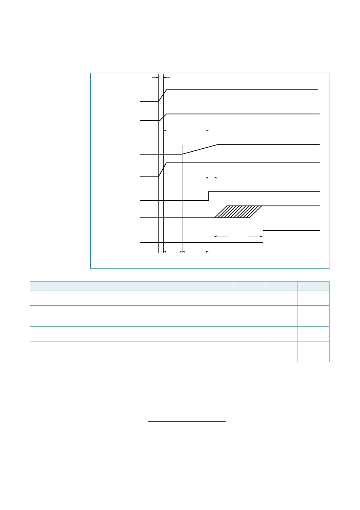
14.3 IC startup timing with PWRON pulled up
The PF8101/PF8201 features a fast internal core power up sequence to fulfill system
power up timings of 5.0 ms or less, from power application until MCU is out of reset.
Such requirement needs a maximum ramp up time of 1.5 ms for VIN to cross the UVDET
threshold in the rising edge.
A maximum core biasing time of 1.5 ms from VIN crossing to UVDET until the beginning
of the power up sequence is ensured to allow up to 1.5 ms time frame for the voltage
regulators power up sequence.
Timing for the external regulators to start up is programmed by default in the OTP fuses.
The 5.0 ms power up timing requirement is only applicable when the PWRON pin
operates in level sensitive mode OTP_PWRON_MODE = 0, however turn on timing is
expected to be the same for both level or edge sensitive modes after the power on event
is present.
In applications using the VSNVS regulator, if VSNVS is required to reach regulation
before system regulators come up, the system should use the SEQ[7:0] bits to delay the
system regulators to allow enough time for VSNVS to reach regulation before the power
up sequence is started.
[1]
5.55 5.8 6.0 V
[1]
— — 200 mV
PF8101_PF8201 All information provided in this document is subject to legal disclaimers. © NXP B.V. 2021. All rights reserved.
Product data sheet Rev. 4 — 24 February 2021
22 / 126
Page 23
NXP Semiconductors
aaa-028052
t
reg2reset
t
first
Self
Test
RESETBMCU
Regulator Outputs
(enable signals)
STEST done
(internal signal)
PWRON
VSNVS
V1P5D
UVDET
VIN
Fuse
Load
1.6 V
t
stest_done
Final VSNVS Regulation
t
vin_rise
9-channel power management integrated circuit for high performance applications
PF8101; PF8201
Figure 6. Startup with PWRON pulled up
Table 16. Startup timing requirements (PWRON pulled up)
Symbol Parameter Min Typ Max Unit
t
vin_rise
Rise time of VIN from VPWR application to
10 — 1500 µs
UVDET (system dependent)
t
stest_done
Time from VIN crossing UVDET to STEST_
— — 1.4 ms
done going high (self-test performed and
passed)
t
first
Time from STEST_done to first slot of power up
— — 100 µs
sequence
t
reg2reset
[1] External regulators power up sequence time (t
time to ensure power up within 5.0 ms.
Time from first regulator enabled to
RESETBMCU asserted to guarantee 5.0 ms
PMIC boot up
14.4 IC startup timing with PWRON pulled low during VIN application
It is possible that PWRON is held low when VIN is applied. By default, LPM_OFF bit is
) is programmed by OTP and may be longer than 1.5 ms. However, 1.5 ms is the maximum allowed
reg2reset
[1]
— — 1.5 ms
reset to 0 upon crossing UVDET, therefore the PF8101/PF8201 remains in the LP_Off
state as described in Section 13.1.2 "LP_Off state". In this scenario, quiescent current
in the LP_Off state is kept to a minimum. When PWRON goes high with LPM_OFF = 0,
the PMIC startup is expected to take longer, since it has to enable most of the internal
circuits and perform the self-test before starting a power up sequence.
Figure 7 shows startup timing with LPM_OFF = 0.
PF8101_PF8201 All information provided in this document is subject to legal disclaimers. © NXP B.V. 2021. All rights reserved.
Product data sheet Rev. 4 — 24 February 2021
23 / 126
Page 24
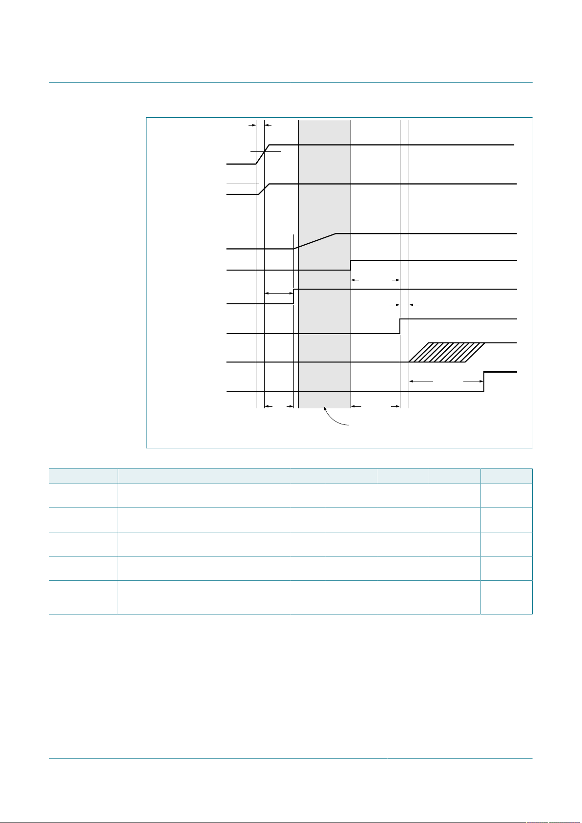
NXP Semiconductors
aaa-028053
t
reg2reset
LP_OFF State
t
first
t
pwrup_lpm
Self-Test
RESETBMCU
Regulator Outputs
Fuse load done
(internal signal)
STEST done
(internal signal)
PWRON
VSNVS
V1P5D
UVDET
VIN
Fuse
Load
t
fuseLoad
1.6 V
Final Regulation
t
vin_rise
9-channel power management integrated circuit for high performance applications
PF8101; PF8201
Figure 7. Startup with PWRON driven high externally and bit LPM_OFF = 0
Table 17. Startup with PWRON driven high externally and LPM_OFF = 0
Symbol Parameter Min Typ Max Unit
t
vin_rise
Rise time of VIN from VPWR application to
10 — 1500 µs
UVDET (system dependent)
t
fuseload
t
pwrup_lpm
t
first
t
reg2reset
Time from VIN crossing UVDET to Fuse_Load_
done (fuse loaded correctly)
Time from PWRON going high to the STEST_
done (self-test performed and passed)
Time from STEST_done to first slot of power up
sequence
Time from first regulator enabled to
— — 600 µs
— — 700 µs
— — 100 µs
[1]
— — 1.5 ms
RESETBMCU asserted to guarantee 5.0 ms
PMIC boot up
[1] External regulators power up sequence time (t
) is programmed by OTP and may be longer than 1.5 ms.
reg2reset
14.5 Power up
14.5.1 Power up events
Upon a power cycle (VIN > UVDET), the LPM_OFF bit is reset to 0, therefore the device
moves to the LP_Off state by default. The actual value of the LPM_OFF bit can be
changed during the run mode and is maintained until VIN crosses the UVDET threshold.
PF8101_PF8201 All information provided in this document is subject to legal disclaimers. © NXP B.V. 2021. All rights reserved.
Product data sheet Rev. 4 — 24 February 2021
24 / 126
Page 25

NXP Semiconductors
9-channel power management integrated circuit for high performance applications
In either one of the off modes, the PF8101/PF8201 can be enabled by the following
power up events:
1. When OTP_PWRON_MODE = 0, PWRON pin is pulled high.
2. When OTP_PWRON_MODE = 1, PWRON pin experiences a high to low transition
A power up event is valid only if:
• VIN > UVDET
• VIN < VIN_OVLO (unless the OVLO is disabled or OTP_VIN_OVLO_SDWN = 0)
• Tj < thermal shutdown threshold
• TRIM_NOK = 0 && OTP_NOK = 0 && STEST_NOK = 0
14.5.2 Power up sequencing
The power up sequencer controls the time and order in which the voltage regulators and
other controlling I/O are enabled when going from the off mode into the run state.
The OTP_SEQ_TBASE[1:0] bits set the default time base for the power up and power
down sequencer.
PF8101; PF8201
and remains low for as long as the PWRON_DBNC timer.
The SEQ_TBASE[1:0] bits can be modified during the system-on states in order to
change the sequencer timing during run/standby transitions as well as the power down
sequence.
Table 18. Power up time base register
OTP bits
OTP_SEQ_TBASE[1:0]
00 00 30
01 01 120
10 10 250
11 11 500
Functional bits
SEQ_TBASE[1:0]
Sequencer time base
(µs)
The power up sequence may include any of the following:
• Switching regulators
• LDO Regulators
• PGOOD pin if programmed as a GPO
• RESETBMCU
The default sequence slot for each one of these signals is programmed via the OTP
configuration registers. And they can be modified in the functional I2C register map to
change the order in which the sequencer behaves during the run/standby transitions as
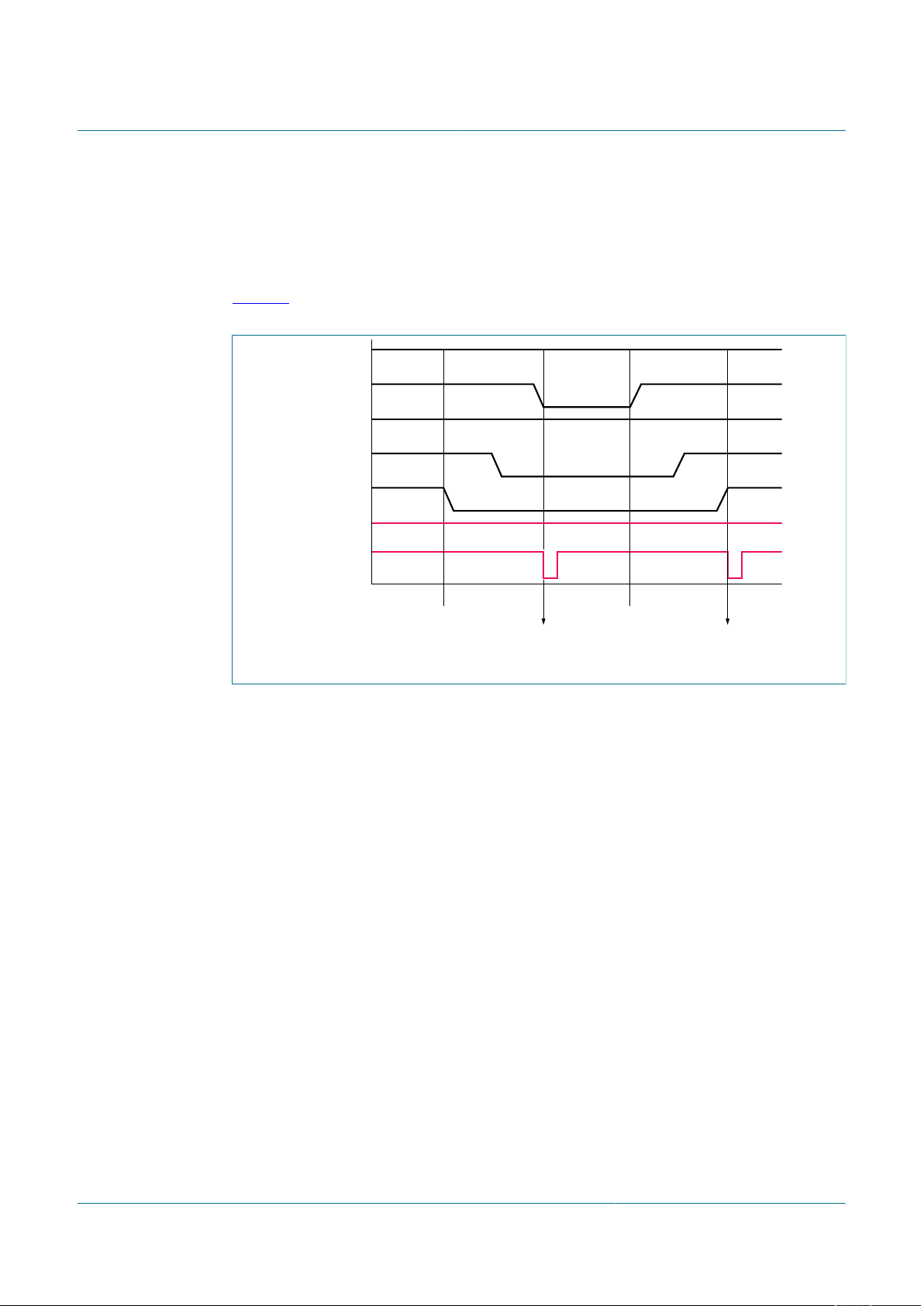
well as the power down sequence.
The _SEQ[7:0] bits set the regulator/pin sequence from 0 to 254. Sequence code 0x00
indicates that the particular output is not part of the startup sequence and remains in off
(in case of a regulator) or remains low/disabled (in case of PGOOD pin used as a GPO).
PF8101_PF8201 All information provided in this document is subject to legal disclaimers. © NXP B.V. 2021. All rights reserved.
Product data sheet Rev. 4 — 24 February 2021
25 / 126
Page 26
NXP Semiconductors
aaa-028054
System On
End of
PWRUP
End of
PWRDN
Power down Seq.
Run to Off
Power up Seq.
Off to Run
INTB
LDO2
SW2
SW5
LDO1
SW1
RESETBMCU
Start of
PWRDN
9-channel power management integrated circuit for high performance applications
Table 19. Power up sequence registers
OTP bits
OTP_SWx_SEQ[7:0]/
OTP_LDOx_SEQ[7:0]/
OTP_PGOOD_SEQ[7:0]/
OTP_RESETBMCU_SEQ[7:0]
00000000 00000000 Off Off
00000001 00000001 0 SLOT0
00000010 00000010 1 SEQ_TBASE x SLOT1
.
.
.
11111111 11111111 254 SEQ_TBASE x SLOT254
If RESETBMCU is not programmed in the OTP sequence, it will be enabled by default
after the last regulator programmed in the power up sequence.
When the _SEQ[7:0] bits of all regulators and PGOOD used as a GPIO are set to 0x00
(off) and a power on event is present, the device moves to the run state in slave mode.
In this mode, the device is enabled without any voltage regulator or GPO enabled. If the
RESETBMCU is not programed in a power up sequence slot, it is released when the
device enters the run state.
Functional bits
SWx_SEQ[7:0]/
LDOx_SEQ[7:0]/
PGOOD_SEQ[7:0]/
RESETBMCU_SEQ[7:0]
.
.
.
PF8101; PF8201
Sequence slot Startup time
.
.
.
(µs)
(right after PWRON event is
valid)
.
.
.
The slave mode is a special case of the power up sequence to address the scenario
where the PF8101/PF8201 is working as a slave PMIC, and supplies are meant to be
enabled by the MCU during the system operation. In this scenario, if RESETBMCU is
used, it is connected to the master RESETBMCU pin.
The PWRUP_I interrupt bit is asserted at the end of the power up sequence when the
time slot of the last regulator in the sequence has ended.
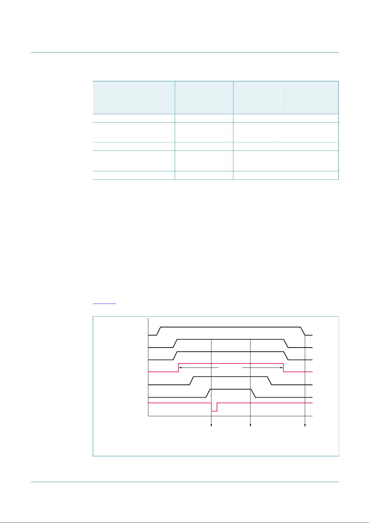
Figure 8 provides an example of the power up/down sequence coming from the off
modes.
Figure 8. Power up/down sequence between off and system-on states
PF8101_PF8201 All information provided in this document is subject to legal disclaimers. © NXP B.V. 2021. All rights reserved.
Product data sheet Rev. 4 — 24 February 2021
26 / 126
Page 27
NXP Semiconductors
aaa-028055
PWRUP_lPWRDN_l
Run
Mode
STBY
Mode
PWRDN Sequence
from Run to STBY
PWRUP Sequence
from STBY to Run
INTB
RESETBMCU
LDO2
SW5
SW2
SW1
LDO1
9-channel power management integrated circuit for high performance applications
When transitioning from standby mode to run mode, the power up sequencer is activated
only if any of the external regulators is re-enabled during this transition. If none of the
regulators toggle from off to on and only voltage changes are being performed when
entering or exiting standby mode, the changes for the voltage regulators are made
simultaneously rather than going through the power up sequencer.
Figure 9 shows an example of the power up/down sequence when transitioning between
run and standby modes.
PF8101; PF8201
Figure 9. Power up/down sequence between run and standby
The PWRUP_I interrupt is set while transitioning from standby to run, even if the
sequencer is not used. This is used to indicate that the transition is complete and device
is ready to perform proper operation.
14.6 Power down
14.6.1 Turn off events
Turn off events may be requested by the MCU (non-PMIC fault related) or due to a
critical failure of the PMIC (hard fault condition).
The following are considered non-PMIC failure turn off events:
1. When OTP_PWRON_MODE = 0, the device starts a power down sequence when the
PWRON pin is pulled low.
2. When OTP_PWRON_MODE = 1, the device starts a power down sequence when
the PWRON pin sees a transition from high to low and remains low for longer than
TRESET.
3. When bit PMIC_OFF is set to 1, the device starts a 500 µs shutdown timer. When the
shutdown timer is started, the PF8101/PF8201 sets the SDWN_I interrupt and asserts
the INTB pin provided it is not masked. At this point, the MCU can read the interrupt
and decide whether to continue with the turn off event or stop it in case it was sent by
mistake.
If the SDWN_I bit is cleared before the 500 µs shutdown timer is expired, the
shutdown request is cancelled and the shutdown timer is reset; otherwise, if the
shutdown timer is expired, the PF8101/PF8201 starts a power down sequence.
PF8101_PF8201 All information provided in this document is subject to legal disclaimers. © NXP B.V. 2021. All rights reserved.
Product data sheet Rev. 4 — 24 February 2021
27 / 126
Page 28

NXP Semiconductors
9-channel power management integrated circuit for high performance applications
The PMIC_OFF bit self-clears after SDWN_I flag is cleared.
4. When VIN_OVLO_EN = 1 and VIN_OVLO_SDWN = 1, and a VIN_OVLO event is
present.
Turn off events due to a hard fault condition:
1. If an OV, UV or ILIM condition is present long enough for the fault timer to expire.
2. In the event that an OV, UV or ILIM condition appears and clears cyclically, and the
FAULT_CNT[3:0] = FAULT_MAX_CNT[3:0].
3. If the watchdog fail counter is overflown, that is WD_EVENT_CNT = WD_MAX_CNT.
4. When Tj crosses the thermal shutdown threshold as the temperature rises.
When the PF8101/PF8201 experience a turn off event due to a hard fault condition, the
devices pass through the fail-safe transition after regulators have been powered down.
14.6.2 Power down sequencing
During a power down sequence, output voltage regulators can be turned off in two
different modes as defined by the PWRDWN_MODE bit.
1. When PWRDWN_MODE = 0, the regulators power down in sequential mode.
2. When PWRDWN_MODE = 1, the regulators power down by groups.
PF8101; PF8201
During transition from run to standby, the power down sequencer is activated in the
corresponding mode. If any of the external regulators are turned off in the standby
configuration. If external regulators are not turned off during this transition, the power
down sequencer is bypassed and the transition happens at once (any associated DVS
transitions could still take time).
The PWRDN_I interrupt is set at the end of the transition from run to standby when the
last regulator has reached its final state, even if external regulators are not turned off
during this transition.
14.6.2.1 Sequential power down
When the device is set to the sequential power down, it uses the same _SEQ[7:0]
registers as the power up sequence to power down in reverse order.
All regulators with the _SEQ[7:0] bits set to 0x00, power down immediately and the
remaining regulators power down one OTP_SEQ_TBASE[1:0] delay after, in reverse
order as defined in the _SEQ[7:0] bits.
If PGOOD pin is used as a GPO, it is de-asserted as part of the power down sequence
as indicated by the PGOOD_SEQ[7:0] bits.
If the MCU requires a different power down sequence, it can change the values of the
SEQ_TBASE[1:0] and the _SEQ[7:0] bits during the system-on states.
When the state machine pass through any of the off modes, the contents of the
SEQ_TBASE[1:0] and _SEQ[7:0] bits are reloaded with the corresponding mirror register
(OTP) values before it starts the next power up sequence.
14.6.2.2 Group power down
When the device is configured to power down in groups, the regulators are assigned to a
specific power down group. All regulators assigned to the same group are disabled at the
same time when the corresponding group is due to be disabled.
PF8101_PF8201 All information provided in this document is subject to legal disclaimers. © NXP B.V. 2021. All rights reserved.
Product data sheet Rev. 4 — 24 February 2021
28 / 126
Page 29

NXP Semiconductors
9-channel power management integrated circuit for high performance applications
Power down groups shut down in decreasing order starting from the lowest hierarchy
group with a regulator shutting down (for instance, Group 4 being the lowest hierarchy
and Group 1 the highest hierarchy group). If no regulators are set to the lowest hierarchy
group, the power down sequence timer starts off the next available group that contains a
regulator to power down.
Each regulator has its own _PDGRP[1:0] bits to set the power down group it belongs to
as shown in Table 20.
Table 20. Power down regulator group bits
OTP_SWx_PDGRP[1:0]
OTP_LDOx_PDGRP[1:0]
OTP_PGOOD_PDGRP[1:0]
OTP_RESETBMCU_PDGRP[1:0]
00 00 Regulator belongs to Group 4
01 01 Regulator belongs to Group 3
10 10 Regulator belongs to Group 2
11 11 Regulator belongs to Group 1
If PGOOD pin is used as a GPO, the PGOOD_PDGRP[1:0] is used to turn off the
PGOOD pin in a specific group during the power down sequence. If PGOOD pin is used
in power good mode, it is recommended that the OTP_PGOOD_PDGRP bits are set
to 11 to ensure the group power down sequencer does not detect these bits as part of
Group 4.
SWx_PDGRP[1:0]
LDOx_PDGRP[1:0]
PGOOD_PDGRP[1:0]
RESETBMCU_PDGRP[1:0]
PF8101; PF8201
Description
Each one of power down groups have programmable time delay registers to set the time
delay after the regulators in this group have been turned off, and the next group can start
to power down.
Table 21. Power down counter delay
OTP bits
OTP_GRPx_DLY[1:0]
00 00 120
01 01 250
10 10 500
11 11 1000
Functional bits
GRPx_DLY[1:0]
Power down delay
(µs)
If RESETBMCU is required to be asserted first before any of the external regulators from
the corresponding group, the RESETBMCU_DLY provides a selectable delay to disable
the regulators after RESETBMCU is asserted.
Table 22. Programmable delay after RESETBMCU is asserted
OTP bits
OTP_RESETBMCU_DLY[1:0]
00 00 No delay
01 01 10
10 10 100
11 11 500
Functional bits
RESETBMCU_DLY[1:0]
RESETBMCU delay
(µs)
If RESETBMCU_DLY is set to 0x00, all regulators in the same power down group as
RESETBMCU is disabled at the same time RESETBMCU is asserted.
PF8101_PF8201 All information provided in this document is subject to legal disclaimers. © NXP B.V. 2021. All rights reserved.
Product data sheet Rev. 4 — 24 February 2021
29 / 126
Page 30
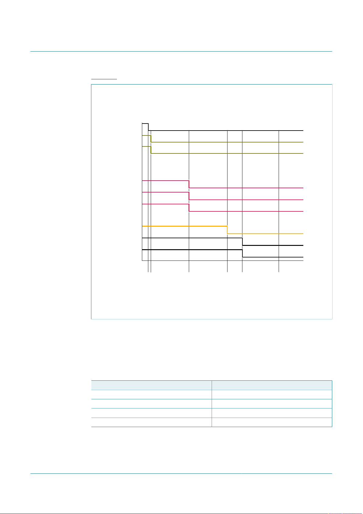
NXP Semiconductors
aaa- 029319
120 µs
GRP3 _DLY
120 µs
GRP2_DLY
120 µs
GRP1_DLY
PWRDN EVENT
GRP3 SDWN
RESETB MCU
asser ted
GRP1 SDW N
SUPPLIES
End of Power
Down
GRP2 SDWN
10 µs
PWRON
PDWN_GRP1
GPR1_DLY = 120 µs
SW1
LDO1
RESETB MCU_ DLY = 10 µS
PDWN_GRP2
GPR2 _DLY = 120 µs
SW2
SW5
SW6
PDWN_GRP3
GPR3_ DLY = 120 µs
LDO2
LDO3
NA
PDWN_GRP4
LDO2
LDO3
SW2
SW5
SW6
RESETB MCU
SW1
LDO1
9-channel power management integrated circuit for high performance applications
Figure 10 shows an example of the power down sequence when PWRDWN_MODE = 1.
PF8101; PF8201
PF8101_PF8201 All information provided in this document is subject to legal disclaimers. © NXP B.V. 2021. All rights reserved.
Product data sheet Rev. 4 — 24 February 2021
Figure 10. Group power down sequence example
14.6.2.3 Power down delay
After a power down sequence is started, the PWRON pin shall be masked until the
sequence is finished and the programmable power down delay is reached, then the
device can power up again if a power-up event is present. The power down delay time
can be programed on OTP via the OTP_PD_SEQ_DLY[1:0] bits.
Table 23. Power down delay selection
OTP_PD_SEQ_DLY[1:0] Delay after power down sequence
00 No delay
01 1.5 ms
10 5.0 ms
11 10 ms
30 / 126
Page 31

NXP Semiconductors
aaa-029211
regulator
outputs
shutdown
event
PWRON
VSNVS
RESETBMCU
power down delay
power down
sequence
power down
sequence
power down
delay
system on
state
OFF state
9-channel power management integrated circuit for high performance applications
Figure 11. Power down delay
PF8101; PF8201
The default value of the OTP_PD_SEQ_DLY[1:0] bits on an unprogrammed OTP device
shall be 00.
14.7 Fault detection
Three types of faults are monitored per regulator: UV, OV and ILIM. Faults are monitored
during power up sequence, run, standby and WD reset states. A fault event is notified to
the MCU through the INTB pin if the corresponding fault is not masked.
The fault configuration registers are reset to their default value after the power up
sequences, and system must configure them as required during the boot-up process via
I2C commands.
For each type of fault, there is an I2C bit that is used to select whether the regulator is
kept enabled or disabled when the corresponding regulator experience a fault event.
SWx_ILIM_STATE / LDOx_ILIM_STATE
• 0 = regulator disable upon an ILIM fault event
• 1 = regulator remains on upon an ILIM fault event
SWx_OV_STATE / LDOx_OV_STATE
• 0 = regulator disable upon an OV fault event
• 1 = regulator remains on upon an OV fault event
SWx_UV_STATE / LDOx_UV_STATE
PF8101_PF8201 All information provided in this document is subject to legal disclaimers. © NXP B.V. 2021. All rights reserved.
Product data sheet Rev. 4 — 24 February 2021
• 0 = regulator disable upon an UV fault event
• 1 = regulator remains on upon an UV fault event
The following table lists the functional bits associated with enabling/disabling the external
regulators when they experience a fault.
31 / 126
Page 32

NXP Semiconductors
RegX_STATE = 0 && Regx_FLT_REN = 0
ILIM fault
RegX_STATE = 0 && Regx_FLT_REN = 0
OV/UV fault
User
Enabled
300 µs
PGOOD
REGx
I_REGx
REGx_EN
RegX_PG
REGx_EN
REGx
User
Enabled
ILIM
1 ms
aaa-028057
9-channel power management integrated circuit for high performance applications
Table 24. Regulator control during fault event bits
Regulator Bit to disable the
SW1 SW1_ILIM_STATE SW1_UV_STATE SW1_OV_STATE
SW2 SW2_ILIM_STATE SW2_UV_STATE SW2_OV_STATE
SW5 SW5_ILIM_STATE SW5_UV_STATE SW5_OV_STATE
SW6 SW6_ILIM_STATE SW6_UV_STATE SW6_OV_STATE
SW7 SW7_ILIM_STATE SW7_UV_STATE SW7_OV_STATE
LDO1 LDO1_ILIM_STATE LDO1_UV_STATE LDO1_OV_STATE
LDO2 LDO2_ILIM_STATE LDO2_UV_STATE LDO2_OV_STATE
LDO3 LDO3_ILIM_STATE LDO3_UV_STATE LDO3_OV_STATE
ILIM faults are debounced for 1.0 ms before they can be detected as a fault condition. If
the regulator is programed to disable upon an ILIM condition, the regulator turns off as
soon as the ILIM condition is detected.
OV/UV faults are debounced as programmed by the OV_DB and UV_DB registers,
before they are detected as a fault condition. If the regulator is programmed to disable
upon an OV or UV, the regulator will turn off if the fault persist for longer than 300 µs after
the OV/UV fault has been detected.
regulator during current
limit
PF8101; PF8201
Bit to disable the
regulator during
undervoltage
Bit to disable the
regulator during
overvoltage
Figure 12. Regulator turned off with RegX_STATE = 0 and FLT_REN = 0
When a regulator is programmed to disable upon an OV, UV, or ILIM fault, a bit is
provided to decide whether a regulator can return to its previous configuration or remain
disabled when the fault condition is cleared.
SWx_FLT_REN / LDOx_FLT_REN
PF8101_PF8201 All information provided in this document is subject to legal disclaimers. © NXP B.V. 2021. All rights reserved.
Product data sheet Rev. 4 — 24 February 2021
32 / 126
Page 33

NXP Semiconductors
RegX_STATE = 0 && FLT_REN = 1
ILIM fault
RegX_STATE = 0 && FLT_REN = 1
OV/UV fault
REGx
I_REGx
REGx_EN
REGx
REGx_EN
PGOOD
REGx_PG
ILIM
1 ms 1.5 ms
500 µs
300 µs
500 µs
300 µs
1 ms 1.5 ms
aaa-028058
9-channel power management integrated circuit for high performance applications
• 0 = regulator remains disabled after the fault condition is cleared or no longer present
• 1 = regulator returns to its previous state if fault condition is cleared
If a regulator is programmed to remain disabled after clearing the fault condition,
the MCU can turn it back on during the system on states by toggling off and on the
corresponding mode/enable bits.
When the bit SWx_FLT_REN = 1, if a regulator is programmed to turn off upon an OV,
UV or ILIM condition, the regulator returns to its previous state 500 µs after the fault
condition is cleared. If the regulator is programmed to turn off upon an ILIM condition, the
device may take up to 1.0 ms to debounce the ILIM condition removal, in addition to the
500 µs wait period to re-enable the regulator.
PF8101; PF8201
Figure 13. Regulator turned off with RegX_STATE = 0 and FLT_REN = 1
When the LDO2 is controlled by hardware using the LDO2EN pin and programmed to
turn off upon an OV, UV or ILIM fault, the LDO2_FLT_REN bit still controls whether the
regulator returns to its previous state or not regardless the state of the LDO2EN pin.
If LDO2 controlled by LDO2EN pin is instructed to remain disabled by the
LDO2_FLT_REN bit, it recovers hardware control by modifying the LDO2_EN bits in the
I2C register maps. See Section 14.9.10 "LDO2EN" for details on hardware control of
LDO2 regulator.
To avoid fault cycling, a global fault counter is provided. Each time any of the external
regulators encounter a fault event, the PF8101/PF8201 compares the value of the
FAULT_CNT[3:0] against the FAULT_MAX_CNT, and if it not equal, it increments the
FAULT_CNT[3:0] and proceeds with the fault protection mechanism.
The processor is expected to read the counter value and reset it when the faults have
been cleared and the device returns to a normal operation. If the processor does not
reset the fault counter and it equals the FAULT_MAX_CNT[3:0] value, the state machine
initiates a power down sequence.
PF8101_PF8201 All information provided in this document is subject to legal disclaimers. © NXP B.V. 2021. All rights reserved.
Product data sheet Rev. 4 — 24 February 2021
The default value of the FAULT_MAX_CNT[3:0] is loaded from the
OTP_FAULT_MAX_CNT[3:0] bits during the power up sequence.
33 / 126
Page 34

NXP Semiconductors
9-channel power management integrated circuit for high performance applications
When the FAULT_MAX_CNT[3:0] is set to 0x00, the system disables the turn-off events
due to a Fault Counter maxing out.
When a regulator experiences a fault event, a fault timer is started. While this timer
is in progress, the expectation is that the processor takes actions to clear the fault.
For example, it could reduce its load in the event of a current limit fault, or turn off the
regulator in the event of an overvoltage fault.
If the fault clears before the timer expires, the state machine resumes the normal
operation, and the fault timer gets reset. If the fault does not clear before the timer
expires, a power down sequence is initiated to turn off the voltage regulators.
The default value of the fault timer is set by the OTP_TIMER_FAULT[3:0], however the
duration of the fault timer can be changed during the system on states by modifying the
TIMER_FAULT[3:0] bits in the I2C registers.
Table 25. Fault timer register configuration
OTP bits
OTP_TIMER_FAULT [3:0]
0000 0000 1
0001 0001 2
0010 0010 4
0011 0011 8
0100 0100 16
0101 0101 32
0110 0110 64
0111 0111 128
1000 1000 256
1001 1001 512
1010 1010 1024
1011 1011 2056
1100 1100 Reserved
1101 1101 Reserved
1110 1110 Reserved
1111 1111 Disabled
Functional bits
TIMER_FAULT [3:0]
PF8101; PF8201
Timer value
(ms)
Each voltage regulator has a dedicated I2C bit that is used to bypass the fault detection
mechanism for each specific fault.
SWx_ILIM_BYPASS / LDOx_ILIM_BYPASS
• 0 = ILIM protection enabled
• 1 = ILIM fault bypassed
SWx_OV_BYPASS / LDOx_OV_BYPASS
• 0 = OV protection enabled
• 1 = OV fault bypassed
SWx_UV_BYPASS / LDOx_UV_BYPASS
• 0 = UV protection enabled
• 1 = UV fault bypassed
PF8101_PF8201 All information provided in this document is subject to legal disclaimers. © NXP B.V. 2021. All rights reserved.
Product data sheet Rev. 4 — 24 February 2021
34 / 126
Page 35

NXP Semiconductors
9-channel power management integrated circuit for high performance applications
Table 26. Fault bypass bits
Regulator Bit to bypass a current
SW1 SW1_ILIM_BYPASS SW1_UV_BYPASS SW1_OV_BYPASS
SW2 SW2_ILIM_BYPASS SW2_UV_BYPASS SW2_OV_BYPASS
SW5 SW5_ILIM_BYPASS SW5_UV_BYPASS SW5_OV_BYPASS
SW6 SW6_ILIM_BYPASS SW6_UV_BYPASS SW6_OV_BYPASS
SW7 SW7_ILIM_BYPASS SW7_UV_BYPASS SW7_OV_BYPASS
LDO1 LDO1_ILIM_BYPASS LDO1_UV_BYPASS LDO1_OV_BYPASS
LDO2 LDO2_ILIM_BYPASS LDO2_UV_BYPASS LDO2_OV_BYPASS
LDO3 LDO3_ILIM_BYPASS LDO3_UV_BYPASS LDO3_OV_BYPASS
The default value of the OV_BYPASS, UV_BYPASS and ILIM_BYPASS bits upon power
up can be configured by their corresponding OTP bits.
Bypassing the fault detection prevents the specific fault from starting any of the protective
mechanism:
• Increment the counter
• Start the Fault timer
• Disable the regulator if the corresponding _STATE bit is 0
• OV / UV condition asserting the PGOOD pin low
limit
PF8101; PF8201
Bit to bypass an
undervoltage
Bit to bypass an
overvoltage
When a fault is bypassed, the corresponding interrupt bit is still set and the INTB pin is
asserted, provided the interrupt has not been masked.
14.7.1 Fault monitoring during power up state
An OTP bit is provided to select whether the output of the switching regulators is
verified during the power up sequence and used as a gating condition to release the
RESETBMCU or not.
• When OTP_PG_CHECK = 0, the output voltage of the regulators is not checked during
the power up sequence and power good indication is not required to de-assert the
RESETBMCU. In this scenario, the OV/UV monitors are masked until RESETBMCU
is released; after this event, all regulators may start checking for faults after their
corresponding blanking period.
• When OTP_PG_CHECK = 1, the output voltage of the regulators is verified during
the power up sequence and a power good condition is required to release the
RESETBMCU.
When OTP_PG_CHECK = 1, OV and UV faults during the power up sequence are
reported based on the internal PG (Power Good) signals of the corresponding external
regulator. The PGOOD pin can be used as an external indicator of an OV/UV failure
when the RESETBMCU is ready to be de-asserted and it has been configured in the
PGOOD mode. See Section 14.9.8 "PGOOD" for details on PGOOD pin operation and
configuration.
Regardless of the PGOOD pin configured as a power good indicator or not, the PF8101/
PF8201 masks the detection of an OV/UV failure until RESETBMCU is ready to be
released, at this point the device checks for any OV/UV condition for the regulators
turned on so far. If all regulators powered up before or in the same sequence slot
than RESETBMCU are in regulation, RESETBMCU is de-asserted and the power up
sequence can continue as shown in Figure 14.
PF8101_PF8201 All information provided in this document is subject to legal disclaimers. © NXP B.V. 2021. All rights reserved.
Product data sheet Rev. 4 — 24 February 2021
35 / 126
Page 36

NXP Semiconductors
aaa-028059
RESETBMCU
REG4_PG
REG3_PG
REG2_PG
SEQ SLOT 1
SEQ SLOT 2
SEQ SLOT 3
SYSTEM ON
PG' sOK
REG4
REG3
REG2
REG1_PG
REG1
PGOOD
(optional)
9-channel power management integrated circuit for high performance applications
PF8101; PF8201
Figure 14. Correct power up (no fault during power up)
If any of the regulators are powered up before RESETBMCU is out of regulator,
RESETBMCU is not de-asserted and the power up sequence is stopped for up to 2.0 ms.
If the fault is cleared and all internal PG signals are asserted within the 2.0 ms timer,
RESETBMCU is de-asserted and the power up sequence continues where it stopped as
shown in Figure 15.
PF8101_PF8201 All information provided in this document is subject to legal disclaimers. © NXP B.V. 2021. All rights reserved.
Product data sheet Rev. 4 — 24 February 2021
36 / 126
Page 37

NXP Semiconductors
aaa-028060
RESETBMCU
REG4_PG
REG3_PG
REG2_PG
SEQ SLOT 1
SEQ SLOT 2
SEQ SLOT 3
SYSTEM ON
Regulator
Recovery
< 2 ms
PG's NOK
REG4
REG3
REG2
REG1_PG
REG1
PGOOD
(optional)
9-channel power management integrated circuit for high performance applications
PF8101; PF8201
Figure 15. Power up sequencer with a temporary failure
If the faulty condition is not cleared within the 2.0 ms timer, the power up sequence is
aborted and the PF8101/PF8201 turn off all voltage regulators enabled so far as shown
in Figure 16.
PF8101_PF8201 All information provided in this document is subject to legal disclaimers. © NXP B.V. 2021. All rights reserved.
Product data sheet Rev. 4 — 24 February 2021
37 / 126
Page 38

NXP Semiconductors
aaa-028061
RESETBMCU
REG4_PG
REG3_PG
REG2_PG
SEQ SLOT 1
SEQ SLOT 2
SEQ SLOT 3
PWRUP Fail
Reg Power down2 ms (max)
Recovery
PG's NOK
REG4
REG3
REG2
REG1_PG
REG1
PGOOD
(optional)
9-channel power management integrated circuit for high performance applications
PF8101; PF8201
Figure 16. Power up sequencer aborted as fault persists for longer than 2.0 ms
Supplies enabled after RESETBMCU are checked for OV, UV and ILIM faults after
each of them is enabled. If an OV, UV or ILIM condition is present, the PF8101/PF8201
starts a fault detection and protection mechanism as described in Section 14.7 "Fault
detection". At this point, the MCU should be able to read the interrupt and react upon a
fault event as defined by the system.
When OTP_PG_CHECK=1, if PGOOD is used as a GPIO, it may be released at any time
in the power up sequence as long as the RESETBMCU is released after one or more of
the SW or LDO regulators.
If a regulator fault occurs after RESETBMCU is de-asserted but before the power
up sequence is finalized, the power up sequence continues to turn on the remaining
regulators as configured, even if a fault detection mechanism is active on an earlier
regulator.
14.8 Interrupt management
The MCU is notified of any interrupt through the INTB pin and various interrupt registers.
The interrupt registers are composed by three types of bits to help manage all the
interrupt requests in the PF8101/PF8201:
• The interrupt latch XXXX_I: this bit is set when the corresponding interrupt event
occurs. It can be read at any time, and is cleared by writing a 1 to the bit.
• The mask bit XXXX_M: this bit controls whether a given interrupt latch pulls the INTB
pin low or not.
• When the mask bit is 1, the interrupt latch does not control the INTB pin.
PF8101_PF8201 All information provided in this document is subject to legal disclaimers. © NXP B.V. 2021. All rights reserved.
Product data sheet Rev. 4 — 24 February 2021
38 / 126
Page 39

NXP Semiconductors
9-channel power management integrated circuit for high performance applications
• When the mask bit is 0, INTB pin is pulled low as long as the corresponding latch bit is
set.
• The sense bit XXXX_S: if available, the sense bit provides the actual status of the
signal triggering the interrupt.
The INTB pin is a reflection of an “OR” logic of all the interrupt status bits which control
the pin.
Interrupts are stored in two levels on the interrupts registers. At first level, the SYS_INT
register provides information about the Interrupt register that originated the interrupt
event.
The corresponding SYS_INT bits will be set as long as the INTB pin is programmed to
assert with any of the interrupt bits of the respective interrupt registers.
• STATUS1_I: this bit is set when the interrupt is generated within the INT STATUS1
register
• STATUS2_I: this bit is set when the interrupt is generated within the INT STATUS2
register
• MODE_I: this bit is set when the interrupt is generated within the SW MODE INT
register
• ILIM_I: this bit is set when the interrupt is generated within any of the SW ILIM INT or
LDO ILIM INT registers
• UV_I: this bit is set when the interrupt is generated within any of the SW UV INT or
LDO UV INT registers
• OV_I: this bit is set when the interrupt is generated within any of the SW OV INT or
LDO OV INT registers
• PWRON_I: this bit is set when the interrupt is generated within the PWRON INT
register
• EWARN_I: is set when an early warning event occurs to indicate an imminent
shutdown
PF8101; PF8201
The SYS_INT bits are set when the INTB pin is asserted by any of the second level
interrupt bits that have not been masked in their corresponding mask registers. When
the second level interrupt bit is cleared, the corresponding first level interrupt bit on the
SYS_INT register will be cleared automatically.
The INTB pin will remain asserted if any of the first level interrupt bit is set, and it will be
de-asserted only when all the unmasked second level interrupts are cleared and thus all
the first level interrupts are cleared as well.
At second level, the remaining registers provide the exact source for the interrupt event.
Table 27 shows a summary of the interrupt latch, mask and sense pins available on the
PF8101/PF8201.
Table 27. Interrupt registers
Register name BIT7 BIT6 BIT5 BIT4 BIT3 BIT2 BIT1 BIT0
INT STATUS1 SDWN_I FREQ_RDY_I CRC_I PWRUP_I PWRDN_I XINTB_I FSOB_I VIN_OVLO_I
INT MASK1 SDWN_M FREQ_RDY_M CRC_M PWRUP_M PWRDN_M XINTB_M FSOB_M VIN_OVLO_M
INT SENSE1 — — — — — XINTB_S FSOB_S VIN_OVLO_S
THERM INT WDI_I FSYNC_FLT_I THERM_155_I THERM_140_I THERM_125_I THERM_110_I THERM_95_I THERM_80_I
THERM MASK WDI_M FSYNC_FLT_M THERM_155_M THERM_140_M THERM_125_M THERM_110_M THERM_95_M THERM_80_M
THERM SENSE WDI_S FSYNC_FLT_S THERM_155_S THERM_140_S THERM_125_S THERM_110_S THERM_95_S THERM_80_S
SW MODE INT — SW7_MODE_I SW6_MODE_I SW5_MODE_I — — SW2_MODE_I SW1_MODE_I
SW MODE MASK — SW7_MODE_M SW6_MODE_M SW5_MODE_M — — SW2_MODE_M SW1_MODE_M
PF8101_PF8201 All information provided in this document is subject to legal disclaimers. © NXP B.V. 2021. All rights reserved.
Product data sheet Rev. 4 — 24 February 2021
39 / 126
Page 40

NXP Semiconductors
PF8101; PF8201
9-channel power management integrated circuit for high performance applications
Register name BIT7 BIT6 BIT5 BIT4 BIT3 BIT2 BIT1 BIT0
SW ILIM INT — SW7_ILIM_I SW6_ILIM_I SW5_ILIM_I — — SW2_ILIM_I SW1_ILIM_I
SW ILIM MASK — SW7_ILIM_M SW6_ILIM_M SW5_ILIM_M — — SW2_ILIM_M SW1_ILIM_M
SW ILIM SENSE — SW7_ILIM_S SW6_ILIM_S SW5_ILIM_S — — SW2_ILIM_S SW1_ILIM_S
LDO ILIM INT — — — — — LDO3_ILIM_I LDO2_ILIM_I LDO1_ILIM_I
LDO ILIM MASK — — — — — LDO3_ILIM_M LDO2_ILIM_M LDO1_ILIM_M
LDO ILIM SENSE — — — — — LDO3_ILIM_S LDO2_ILIM_S LDO1_ILIM_S
SW UV INT — SW7_UV_I SW6_UV_I SW5_UV_I — — SW2_UV_I SW1_UV_I
SW UV MASK — SW7_UV_M SW6_UV_M SW5_UV_M — — SW2_UV_M SW1_UV_M
SW UV SENSE — SW7_UV_S SW6_UV_S SW5_UV_S — — SW2_UV_S SW1_UV_S
SW OV INT — SW7_OV_I SW6_OV_I SW5_OV_I — — SW2_OV_I SW1_OV_I
SW OV MASK — SW7_OV_M SW6_OV_M SW5_OV_M — — SW2_OV_M SW1_OV_M
SW OV SENSE — SW7_OV_S SW6_OV_S SW5_OV_S — — SW2_OV_S SW1_OV_S
LDO UV INT — — — — — LDO3_UV_I LDO2_UV_I LDO1_UV_I
LDO UV MASK — — — — — LDO3_UV_M LDO2_UV_M LDO1_UV_M
LDO UV SENSE — — — — — LDO3_UV_S LDO2_UV_S LDO1_UV_S
LDO OV INT — — — — — LDO3_OV_I LDO2_OV_I LDO1_OV_I
LDO OV MASK — — — — — LDO3_OV_M LDO2_OV_M LDO1_OV_M
LDO OV SENSE — — — — — LDO3_OV_S LDO2_OV_S LDO1_OV_S
PWRON INT BGMON_I PWRON_8S_I PWRON_4S_I PRON_3S_I PWRON_2S_I PWRON_1S_I PWRON_REL_I PWRON_PUSH_I
PWRON MASK BGMON_M PWRON_8S_M PWRON_4S_M PRON_3S_M PWRON_2S_M PWRON_1S_M PWRON_REL_M PWRON_PUSH_
PWRON SENSE BGMON_S — — — — — — PWRON_S
SYS INT EWARN_I PWRON_I OV_I UV_I ILIM_I MODE_I STATUS2_I STATUS1_I
M
14.9 I/O interface pins
The PF8101/PF8201 PMIC is fully programmable via the I2C interface. Additional
communication between MCU, PF8101/PF8201 and other companion PMIC is provided
by direct logic interfacing including INTB, RESETBMCU, PGOOD, among other pins.
PF8101_PF8201 All information provided in this document is subject to legal disclaimers. © NXP B.V. 2021. All rights reserved.
Product data sheet Rev. 4 — 24 February 2021
40 / 126
Page 41

NXP Semiconductors
aaa-028062
GPIO (optional)
GPIO (optional)
SD1_VSELECT
SD1_PWR_EN_B
V
SEL
E
C
T
L
DO2
E
N
PMIC_ON_REQ
PWR
O
N
EARLY_WARNING E
W
A
R
N
P
GOO
D
FS
O
B
VIN/
VDDIO
VDDIO VDDIO
PMIC_STBY_REQ S
T
A
NDB
Y
RESE
T
B
M
C
U
WDOG_B
i.MX8 MCU
PMIC1 PMIC2
W
D
I
POR_B
VDDIO
VDDIO
IN
TB
INT_B
TB
B
E
N
GPIO (optional)
GPIO (optional)
SD2_VSELECT
SD2_PWR_EN_B
V
SEL
E
C
T
L
DO2
E
N
PWR
O
N
GPIO (optional)
GPIO (optional)
E
W
A
R
N
P
GOO
D
FS
O
B
VIN/
VDDIO
VDDIO VDDIO
S
T
A
NDB
Y
RESE
T
B
M
C
U
W
D
I
IN
TB
TB
B
E
N
XINTB
XINTB
XFAILB
V1P5A
XFAILB
9-channel power management integrated circuit for high performance applications
PF8101; PF8201
Table 28. I/O electrical specifications
Symbol Parameter Min Typ Max Unit
PWRON_ V
PWRON_ V
STANDBY_ V
STANDBY_ V
RESETBMCU_ VOLRESETBMCU low output voltage
INTB_ V
OL
XINTB_ V
XINTB_ V
R
XINTB_PU
WDI_ V
IL
WDI_ V
IH
R
WDI_PD
EWARN_ V
PGOOD_ V
VSELECT_ V
VSELECT_ V
R
VSELECT_PD
Figure 17. I/O interface diagram
IL
IH
IL
IH
OH
OL
PWRON low input voltage — — 0.4 V
PWRON high input voltage 1.4 — 5.5 V
STANDBY low input voltage — — 0.4 V
IL
STANDBY high input voltage 1.4 — 5.5 V
IH
10 mA load current
INTB low output voltage
10 mA load current
XINTB low input voltage — — 0.3*VDDIO V
0
0
XINTB high input voltage 0.7*VDDIO — 5.5 V
VDDIO − 0.5 —
0
XINTB internal pullup resistance 0.475 1.0 — MΩ
WDI low input voltage — — 0.3*VDDIO V
WDI high input voltage 0.7*VDDIO — 5.5 V
WDI internal pull down resistance 0.475 1.0 — MΩ
EWARN high output voltage
2.0 mA load current
PGOOD low output voltage
10 mA load current
VSELECT low input voltage — — 0.3*VDDIO V
IL
VSELECT high input voltage 0.7*VDDIO — 5.5 V
IH
—
—
0.4
0.4
VDDIO
—
0.4
VSELECT internal pull down resistance 0.475 1.0 — MΩ
V
V
V
V
PF8101_PF8201 All information provided in this document is subject to legal disclaimers. © NXP B.V. 2021. All rights reserved.
Product data sheet Rev. 4 — 24 February 2021
41 / 126
Page 42

NXP Semiconductors
PF8101; PF8201
9-channel power management integrated circuit for high performance applications
Symbol Parameter Min Typ Max Unit
LDO2EN_ V
LDO2EN_ V
R
LDO2EN_PD
TBBEN_ V
TBBEN_ V
R
TBBEN_PD
XFAILB_V
XFAILB_V
XFAILB_V
XFAILB_V
FSOB_ V
SCL_ V
SCL_ V
SDA_ V
SDA_ V
SDA_ V
OL
IL
IH
IL
IH
OL
IL
IH
IL
IH
IL
IH
OH
OL
LDO2EN low input voltage — — 0.3*VDDIO V
LDO2EN high input voltage 0.7*VDDIO — 5.5 V
LDO2EN internal pull down resistance 0.475 1.0 — MΩ
TBBEN low input voltage — — 0.4 V
TBBEN high input voltage 1.4 — 5.5 V
TBBEN internal pull down resistance 0.475 1.0 — MΩ
XFAILB low input voltage — — 0.4 V
XFAILB high input voltage 1.4 — 5.5 V
XFAILB high output voltage
Pulled-up to V1P5A
XFAILB low output voltage
10 mA load current
FSOB low output voltage
−10 mA
SCL low input voltage — — 0.3*VDDIO V
SCL high input voltage 0.7*VDDIO — VDDIO V
SDA low input voltage — — 0.3*VDDIO V
SDA high input voltage 0.7*VDDIO — VDDIO V
SDA low output voltage
−20 mA load current
V1P5A − 0.5 —
0
0
0
—
—
—
—
0.4
0.4
0.4
V
V
V
V
14.9.1 PWRON
PWRON is an input signal to the IC that acts as a power up event signal in the PF8101/
PF8201.
The PWRON pin has two modes of operations as programed by the
OTP_PWRON_MODE bit.
When OTP_PWRON_MODE = 0 the PWRON pin operates in level sensitive mode. In
this mode, the device is in the corresponding off mode when the PWRON pin is pulled
low. Pulling the PWRON pin high is a necessary condition to generate a power on event.
PWRON may be pulled up to VSNVS or VIN with an external 100 kΩ resistor if device is
intended to come up automatically with VIN application. See Section 14.5 "Power up" for
details on power up requirements.
When OTP_PWRON_MODE = 1, the PWRON pin operates in edge sensitive mode. In
this mode, PWRON is used as an input from a push button connected to the PMIC.
When the switch is not pressed, the PWRON pin is pulled up to VIN externally through
a 100 kΩ resistor. When the switch is pressed, the PWRON pin should be shorted to
ground. The PWRON_S bit is high whenever the PWRON pin is at logic 0 and is low
whenever the PWRON pin is at logic 1.
The PWRON pin has a programmable debounce on the rising and falling edges as
shown below.
PF8101_PF8201 All information provided in this document is subject to legal disclaimers. © NXP B.V. 2021. All rights reserved.
Product data sheet Rev. 4 — 24 February 2021
42 / 126
Page 43

NXP Semiconductors
9-channel power management integrated circuit for high performance applications
Table 29. PWRON debounce configuration in edge detection mode
Bits Value Falling edge debounce
PWRON_DBNC[1:0] 00 32 32
PWRON_DBNC[1:0] 01 32 32
PWRON_DBNC[1:0] 10 125 32
PWRON_DBNC[1:0] 11 750 32
The default value for the power on debounce is set by the OTP_PWRON_DBNC[1:0]
bits.
Pressing the PWRON switch for longer than the debounce time starts a power on
event as well as generate interrupts which the processor may use to initiate PMIC state
transitions.
During the system-on states, when the PWRON button is pushed (logic 0) for longer than
the debounce setting, the PWRON_PUSH_I interrupt is generated. When the PWRON
button is released (logic 1) for longer than the debounce setting, the PWRON_REL_I
interrupt is generated.
(ms)
PF8101; PF8201
Rising edge debounce
(ms)
The PWRON_1S_I, PWRON_2S_I, PWRON_3S_I, PWRON_4S_I and PWRON_8S_I
interrupts are generated when the PWRON pin is held low for longer than 1, 2, 3, 4 and 8
seconds respectively.
If PWRON_RST_EN = 1, pressing the PWRON for longer than the delay programmed by
TRESET[1:0] forces a PMIC reset. A PMIC reset initiates a power down sequence, wait
for 30 µs to allow all supplies to discharge and then it powers back up with the default
OTP configuration.
If PWRON_RST_EN = 0, the device starts a turn off event after push button is pressed
for longer than TRESET[1:0].
Table 30. TRESET configuration
TRESET[1:0] Time to reset
00 2 s
01 4 s
10 8 s
11 16 s
The default value of the TRESET delay is programmable through the OTP_TRESET[1:0]
bits.
14.9.2 STANDBY
STANDBY is an input signal to the IC, when this pin is asserted, the device enters the
standby mode and when de-asserted, the part exits standby mode.
STANDBY can be configured as active high or active low using the STANDBYINV bit.
Table 31. Standby pin polarity control
STANDBY (pin) STANDBYINV (I2C bit) STANDBY control
0 0 Not in standby mode
0 1 In standby mode
1 0 In standby mode
PF8101_PF8201 All information provided in this document is subject to legal disclaimers. © NXP B.V. 2021. All rights reserved.
Product data sheet Rev. 4 — 24 February 2021
43 / 126
Page 44

NXP Semiconductors
9-channel power management integrated circuit for high performance applications
STANDBY (pin) STANDBYINV (I2C bit) STANDBY control
1 1 Not in standby mode
14.9.3 RESETBMCU
RESETBMCU is an open-drain, active low output used to bring the processor (and
peripherals) in and out of reset.
The time slot RESETBMCU is de-asserted during the power up sequence is programmed
by the OTP_RESETBMCU_SEQ[7:0] bits, and it is a condition to enter the system-on
states.
During the system-on states, the RESETBMCU is de-asserted (pulled high), and it is
asserted (pulled low) as indicated in the power down sequence, when a system power
down or reset is initiated.
In the application, RESETBMCU can be pulled up to VDDIO or VSNVS by a 100 kΩ
external resistor.
14.9.4 INTB
PF8101; PF8201
INTB is an open-drain, active low output. This pin is asserted (pulled low) when any
interrupt occurs, provided that the interrupt is not masked.
INTB is de-asserted after the corresponding interrupt latch is cleared by software, which
requires writing a “1” to the interrupt bit.
An INTB_TEST bit is provided to allow a manual test of the INTB pin. When INTB_TEST
is set to 1, the interrupt pin asserts for 100 µs and then de-asserts to its normal state.
The INTB_TEST bit self-clears to 0 automatically after the test pulse is generated.
In the application, INTB can be pulled up to VDDIO with an external 100 kΩ resistor.
14.9.5 XINTB
XINTB is an input pin used to receive an external interrupt and trigger an interrupt event
on the PF8101/PF8201. It is meant to interact with the INTB pin of a companion PMIC, in
order to simplify MCU interaction to identify the source of the interrupt.
A high to low transition on the XINTB pin sets the XINTB_I interrupt bit and causes the
INTB to be asserted, provided the interrupt is not masked.
The XINTB_S bit follows the actual status of the XINTB pin even when the XINTB_I has
been cleared or the interrupt has been masked.
This pin is internally pulled up to VDDIO with a 1.0 MΩ resistors; therefore, it can be left
unconnected when the XINTB is not used.
14.9.6 WDI
WDI is an input pin to the PF8101/PF8201 and is intended to operate as an external
watchdog monitor.
When the WDI pin is connected to the watchdog output of the processor, this pin is used
to detect a pulse to indicate a watchdog event is requested by the processor. When the
WDI pin is asserted, the device starts a watchdog event to place the PMIC outputs in a
default known state.
PF8101_PF8201 All information provided in this document is subject to legal disclaimers. © NXP B.V. 2021. All rights reserved.
Product data sheet Rev. 4 — 24 February 2021
44 / 126
Page 45

NXP Semiconductors
9-channel power management integrated circuit for high performance applications
The WDI pin is monitored during the system on states. In the off modes and during the
power up sequence, the WDI pin is masked until RESETBMCU is de-asserted.
The WDI can be configured to assert on the rising or the falling edge using the
OTP_WDI_INV bit.
• When OTP_WDI_INV = 0, the device starts a WD event on the falling edge of the WDI.
• When OTP_WDI_INV = 1, the device starts a WD event on the rising edge of the WDI.
A 10 µs debounce filter is implemented on either rising or falling edge detection to
prevent false WDI signals to start a watchdog event.
The OTP_WDI_MODE bit allows the WDI pin to react in two different ways:
• When OTP_WDI_MODE = 1, a WDI asserted performs a hard WD reset.
• When OTP_WDI_MODE = 0, a WDI asserted performs a soft WD reset.
The WDI_STBY_ACTIVE bit allows the WDI pin to generate a watchdog event during the
standby state.
• When WDI_STBY_ACTIVE = 0, asserting the WDI will not generate a watchdog event
during the standby state.
• When WDI_STBY_ACTIVE = 1, asserting the WDI will start a watchdog event during
the standby state.
PF8101; PF8201
The OTP_WDI_STBY_ACTIVE is used to configure whether the WDI is active in the
standby state or not by default upon power up.
See Section 15.11 "Watchdog event management" for details on watchdog event.
14.9.7 EWARN
EWARN is an active high output, used to notify that an imminent power failure is about to
occur. It should be pulled down to GND by a 100 kΩ resistor.
When a power down is initiated due to a fault, the EWARN pin is asserted before the
device starts powering down as defined by the EWARN_TIME[1:0] bits in order to allow
the system to prepare for the imminent shutdown.
The following faults cause the EWARN pin to be asserted:
• Fault timer expired
• FAULT_CNT = FAULT_MAX_CNT
• Thermal Shutdown tJ > TSD
• VIN_OVLO event when VIN_OVLO_SDWN=1
Table 32. EWARN time configuration
OTP_EWARN_TIME[1:0] EWARN delay time
00 100 μs
01 5.0 ms
10 20 ms
11 50 ms
When the EWARN pin is asserted, an interrupt will be generated and the EWARN_I bit
will be set to announce to the system of an imminent shutdown event.
In the Off modes, EWARN remains de-asserted (pulled low).
PF8101_PF8201 All information provided in this document is subject to legal disclaimers. © NXP B.V. 2021. All rights reserved.
Product data sheet Rev. 4 — 24 February 2021
45 / 126
Page 46

NXP Semiconductors
9-channel power management integrated circuit for high performance applications
In the event of a power loss (VIN removed), the EWARN pin is asserted upon crossing
the V
time to prepare for the power loss.
Table 33. Early warning threshold
Symbol Parameter Min Typ Max Unit
V
WARNTH
14.9.8 PGOOD
PGOOD is an open drain output programmable as a Power Good indicator pin or GPO.
In the application, PGOOD can be pulled up to VDDIO with a 100 kΩ resistor.
When OTP_PG_ACTIVE = 0, the PGOOD pin is used as a general purpose output.
As a GPO, during the run state, the state of the pin is controlled by the RUN_PG_GPO
bit in the functional I2C registers:
• When RUN_PG_GPO = 1, the PGOOD pin is high
• When RUN_PG_GPO = 0, the PGOOD pin is low
WARNTH
PF8101; PF8201
threshold to notify to the processor that VIN may be lost and allow some
Early warning threshold 2.7 2.8 2.9 V
During the standby state, the state of the pin is controlled by the STBY_PG_GPO bit in
the functional I2C registers:
• When STBY_PG_GPO = 1, the PGOOD pin is high
• When STBY_PG_GPO = 0, the PGOOD pin is low
When used as a GPO, the PGOOD pin can be enabled high as part of the
power up sequence as programmed by the OTP_SEQ_TBASE[1:0] and the
OTP_PGOOD_SEQ[7:0] bits. If enabled as part of the power up sequence, both the
RUN_PG_GPO and STBY_PG_GPO bits are loaded with 1, otherwise they are loaded
with 0 upon power up.
When OTP_PG_ACTIVE = 1, the PGOOD pin is in Power good (PG) mode and it acts as
a PGOOD indicator for the selected output voltages in the PF8101/PF8201.
There is an individual PG monitor for every regulator. Each monitor provide an internal
PG signal that can be selected to control the status of the PGOOD pin upon an OV or UV
condition when the corresponding SWxPG_EN / LDOxPG_EN bits are set. The status
of the PGOOD pin is a logic AND function of the internal PG signals of the selected
monitors.
• When the PG_EN = 1, the corresponding regulator becomes part of the AND function
that controls the PGOOD pin.
• When the PG_EN = 0, the corresponding regulator does not control the status of the
PGOOD pin.
The PGOOD pin is pulled low when any of the selected regulator outputs falls above
or below the programmed OV/UV thresholds and a corresponding OV/UV interrupt is
generated. If the faulty condition is removed, the corresponding OV_S/UV_S bit goes low
to indicate the output is back in regulation, however, the interrupt remains latched until it
is cleared.
The actual condition causing the interrupt (OV, UV) can be read in the fault interrupt
registers. For more details on handling interrupts, see Section 14.8 "Interrupt
management".
When a particular regulator is disabled (via OTP, or I2C, or by change in state of PMIC
such as going to standby mode), it no longer controls the PGOOD pin.
PF8101_PF8201 All information provided in this document is subject to legal disclaimers. © NXP B.V. 2021. All rights reserved.
Product data sheet Rev. 4 — 24 February 2021
46 / 126
Page 47

NXP Semiconductors
9-channel power management integrated circuit for high performance applications
In the Off mode and during the power up sequence, the PGOOD pin is held low until
RESETBMCU is ready to be released, at this point, the PG monitors are unmasked
and the PGOOD pin is released high if all the internal PG monitors are in regulation.
In the event that one or more outputs are not in regulation by the time RESETBMCU
is ready to de-assert, the PGOOD pin is held low and the PF8101/PF8201 performs
the corresponding fault protection mechanism as described in Section 14.7.1 "Fault
monitoring during power up state".
14.9.9 VSELECT
VSELECT is an input pin used to select the output voltage of LDO2 when bit
VSELECT_EN = 1.
• When VSELECT pin is low, the LDO2 output is programmed to 3.3 V.
• When VSELECT pin is high, the LDO2 output is programmed to 1.8 V.
When VSELECT_EN = 0, the output of LDO2 is given by the VLDO2_RUN[3:0] bits.
When the PF8101/PF8201 is in the standby mode, the output voltage of LDO2 follows
the configuration as selected by the VLDO2_STBY[3:0] bits, regardless of the value of
VSELECT_EN bit.
PF8101; PF8201
The default value of the VSELECT_EN bit is programmed by the OTP_VSELECT_EN bit
in the OTP fuses.
A read only bit is provided to monitor the actual state of the VSELECT pin. When the
VSELECT pin is low, the VSELECT_S bit is 0 and when the VSELECT pin is high, the
VSELECT_S bit is set to 1.
14.9.10 LDO2EN
LDO2EN is an input pin used to enable or disable LDO2 when the bit LDO2HW_EN = 1.
When LDO2HW_EN = 1, the status of LDO2 output can also be controlled by the
LDO2_RUN_EN bit in the run mode or the LDO2_STBY_EN bit in the standby mode.
Table 34. LDO control in run or standby mode
LDO2EN pin LDO2HW_EN bit LDO2_RUN_EN LDO2_
Do not care 0 0 Disabled
Do not care 0 1 Enabled
Do not care 1 0 Disabled
Low 1 1 Disabled
High 1 1 Enabled
The default controlling mode for LDO2 is programed by the OTP_LDO2HW_EN bit in the
OTP fuses.
STBY_EN
LDO2 output
A read only bit is provided to monitor the actual state of the LDO2EN pin. When the
LDO2EN pin is low, the LDO2EN_S bit is 0 and when the LDO2EN pin is high, the
LDO2EN_S bit is set to 1.
14.9.11 FSOB (safety output)
The FSOB pin is a configurable, active low, open drain output used as a safety output to
keep the system in a safe state upon a power up and/or during a specific failure event.
PF8101_PF8201 All information provided in this document is subject to legal disclaimers. © NXP B.V. 2021. All rights reserved.
Product data sheet Rev. 4 — 24 February 2021
47 / 126
Page 48

NXP Semiconductors
9-channel power management integrated circuit for high performance applications
The FSOB pin is externally pulled up to VIN or VDDIO with a 470 kΩ resistor and it is deasserted high in normal operation.
The FSOB pin can be configured in active safe state mode or fault safe state mode as
programmed by the OTP_FSOB_ASS_EN bit in the OTP fuses.
The PF8201 device allows configuration of the FSOB pin to operate in active safe state
or fault safe state modes via the OTP_FSOB_ASS_EN bit in the OTP fuses. Additionally
on the PF8201 device, if the secure I2C write mechanism is enabled, all FSOB flags
require a secure write for them to be cleared (write 1 to clear + RANDOM_GEN read +
RANDOM_CHK write).
In the PF8101 device, the OTP_FSOB_ASS_EN bit is not available, therefore it can only
operate in fault safe state mode.
14.9.11.1 FSOB fault safe state
If the OTP_FSOB_ASS_EN = 0, the active safe state mode is disabled and the FSOB
operate in the fault safe state mode. In this mode, the FSOB pin may still be asserted if
programmed by other fault events.
In the fault safe state mode, the FSOB is de-asserted by default, and can be asserted as
programmed by the FSOB fault selection bits.
PF8101; PF8201
A bit is provided to enable the FSOB to be asserted when a regulator fault (OV, UV, ILIM)
is present.
• If FSOB_SOFTFAULT = 0, the FSOB pin is not asserted by any OV, UV, or ILIM fault.
• If FSOB_SOFTFAULT = 1, an OV, UV, or ILIM fault on any of the regulators causes
the FSOB pin to assert and remain asserted regardless of it being corrected or not, and
also asserts the FSOB_SFAULT_NOK flag.
A bit is provided to enable the FSOB to be asserted when a WD reset occurs due to a
WDI event.
• If FSOB_WDI = 0, the FSOB pin is not asserted by a WDI event.
• If FSOB_WDI = 1, a WDI event causes the FSOB pin to assert and the
FSOB_WDI_NOK flag to be set.
A bit is provided to enable the FSOB to be asserted when a WD reset occurs due to an
internal WD counter fault is present.
• If FSOB_WDC = 0, the FSOB pin is not asserted by a WD reset started by the internal
WD counter.
• If FSOB_WDC = 1, a WD reset is started by the internal WD counter causing the FSOB
pin to be asserted and the FSOB_WDC_NOK flag to be set.
A bit is provided to enable the FSOB to be asserted when a hard fault shutdown has
occurred.
• If FSOB_HARDFAULT = 0, the FSOB pin is not asserted by a hard fault.
• If FSOB_HARDFAULT = 1, any of the hard fault shutdown events cause the FSOB pin
to be asserted and the FSOB_HFAULT_NOK flag to be set.
Any of the following events are considered a hard fault shutdown:
• Fault timer expired
• FAULT_CNT = FAULT_MAX_CNT (regulator fault counter max out)
• WD_EVENT_CNT = WD_MAX_CNT (watchdog event counter max out)
• Power up failure
PF8101_PF8201 All information provided in this document is subject to legal disclaimers. © NXP B.V. 2021. All rights reserved.
Product data sheet Rev. 4 — 24 February 2021
48 / 126
Page 49

NXP Semiconductors
9-channel power management integrated circuit for high performance applications
• Thermal shutdown
The FSOB pin is released when all the FSOB fault flags are cleared or VIN falls below
the UVDET threshold.
14.9.11.2 FSOB active safe state (PF8201 only)
If the OTP_FSOB_ASS_EN = 1, the active safe state mode is enabled.
In the active safe state mode, the FSOB pin is programmed to be asserted low after OTP
fuses are loaded and remain asserted as long as the PMIC is forced in safe state.
In this mode of operation, the PMIC is forced in the safe state under following conditions:
• Any of the ABIST flags are set during the self-test at power up.
• The FSOB_WDI_NOK is set when FSOB is programmed to assert via the FSOB_WDI
bit
• The FSOB_SFAULT_NOK is set when FSOB is programmed to assert via the
FSOB_SOFTFAULT bit
• Hard WD Reset (voltage regulators and RESETBMCU reset)
• Device is in any of the off mode and the RESETBMCU is asserted low
• The FSOB_ASS_NOK flag is asserted
PF8101; PF8201
Each time the PMIC is forced into the safe state, the FSOB pin will be asserted low and
the FSOB_ASS_NOK flag will be set to 1 in order to keep the system in the safe state
until the MCU verify that it is safe to return to normal operation.
During the active safe state mode, the PMIC can exit the safe state and release the
FSOB pin if the following conditions are met:
• RESETBMCU is de-asserted (system on)
• All ABIST flags are all 0 (ABIST OK)
• No regulator faults are present
• The FSOB_WDI_NOK and/or FSOB_SFAULT_NOK faults are cleared if programmed
to be set by the FSOB_WDI and FSOB_SOFTFAULT bits respectively
• All other NOK flags in the FSOB_FLAGS register, including the FSOB_ASS_NOK flag,
are cleared
A soft WD reset may also assert the FSOB pin only if programmed by the FSOB_WDI bit.
Likewise, the FSOB_SOFTFAULT bit can select whether the FSOB pin is asserted as
soon as an OV, UV or ILIM fault is present even when this condition has not yet lead to a
fault shutdown. In this scenario the system is placed in a safe state while the MCU tries
to clear the fault and command the PF8201 to come out of the safe state when all faults
have been cleared.
14.9.12 TBBEN
The TBBEN is an input pin provided to allow the user to program the mirror registers
in order to operate the device with a custom configuration as well as programming the
default values on the OTP fuses.
• When TBBEN pin is pulled low to ground, the device is operating in normal mode.
• When TBBEN pin is pulled high to V1P5D device enables the TBB configuration mode.
See Section 17 "OTP/TBB and default configurations" for details on TBB and OTP
operation.
PF8101_PF8201 All information provided in this document is subject to legal disclaimers. © NXP B.V. 2021. All rights reserved.
Product data sheet Rev. 4 — 24 February 2021
49 / 126
Page 50

NXP Semiconductors
9-channel power management integrated circuit for high performance applications
When TBBEN pin is pulled high to V1P5D the following conditions apply:
• The device uses a fixed I2C device address (0x08)
• Disable the watchdog operation, including WDI monitoring and internal watchdog timer
• Disable the CRC and I2C secure write mechanism while no power up event is present
(TBB/OTP programming mode).
Disabling the watchdog operation may be required for in-line MCU programming where
output voltages are required but watchdog operation should be completely disabled.
14.9.13 XFAILB
XFAILB is a bidirectional pin with an open drain output used to synchronize the power up
and power down sequences of two or more PMIC's. It should be pulled up externally to
V1P5A supply.
The OTP_XFAILB_EN bit is used to enable or disable the XFAILB mode of operation.
• When OTP_XFAILB_EN = 0, the XFAILB mode is disabled and any events on this pin
are ignored
• When OTP_XFAILB_EN = 1, the XFAILB mode is enabled
PF8101; PF8201
When the XFAILB mode is enabled, and the PF8201 has a turn off event generated by
an internal fault, the XFAILB pin is asserted low 20 µs before starting the power down
sequence.
A power down event caused by the following conditions will assert the XFAILB pin:
• Fault timer expired
• FAULT_CNT = FAULT_MAX_CNT (regulator fault counter max out)
• WD_EVENT_CNT = WD_MAX_CNT (watchdog event counter max out)
• Power up failure
• Thermal shutdown
• Hard WD event
The XFAILB pin is forced low during the off mode.
During the system-on states, if the XFAILB pin is externally pulled low, it will detect an
XFAIL event after a 20 µs debounce. When an XFAIL event is detected, the XFAILB pin
is asserted low internally and the device starts a power down sequence.
If a PWRON event is present, the device starts a turn on event and proceeds to release
the XFAILB pin when its ready to start the power up sequence state. If the XFAILB pin
is pulled down externally during the power up event, the PF8201 will stop the power up
sequence until the pin is no longer pulled down externally. This will help both PMIC's to
synchronize the power up sequence allowing it to continue only when both PMIC's are
ready to initiate the power up sequence.
A hard WD event will set the XFAILB pin 20 µs before it starts its power down sequence.
After all regulators outputs have been turned off, the device will release the XFAILB pin
internally after a 30 µs delay, proceed to load the default OTP configuration and wait for
the XFAILB pin to be released externally before it can restart the power up sequence.
PF8101_PF8201 All information provided in this document is subject to legal disclaimers. © NXP B.V. 2021. All rights reserved.
Product data sheet Rev. 4 — 24 February 2021
50 / 126
Page 51

NXP Semiconductors
aaa-029215
bidirectional XFAILB (power up)
power up
sequence
system onQPU_OffLP_Off self-test
RESETBMCU
XFAILB
POWER UP
sequence
states
PWRON
aaa-029214
20 µs
100 µs
bidirectional XFAILB (power down)
system ON
power down
sequence
off mode
POWER DOWN
signal
XFAILB
POWER DOWN
sequence
EWARN
FAULT EVENT
states
9-channel power management integrated circuit for high performance applications
Figure 18. XFAILB behavior during a power up sequence
PF8101; PF8201
Figure 19. XFAILB behavior during a power down sequence
PF8101_PF8201 All information provided in this document is subject to legal disclaimers. © NXP B.V. 2021. All rights reserved.
Product data sheet Rev. 4 — 24 February 2021
51 / 126
Page 52

NXP Semiconductors
aaa-029212
100 µs
PWRON
FAULT EVENT
EWARN
MASTER
PMIC
SLAVE
PMIC
XFAILB
POWER DOWN
signal
POWER DOWN
sequence
POWER UP
sequence
EWARN
XFAILB
POWER DOWN
signal
POWER DOWN
sequence
POWER UP
sequence
20 µs
20 µs
pin externally pulled down
dual PMIC interaction
(fault on master PMIC)
slave ready to start power
up sequence (waiting)
XFAILB
debounced
power up sequence is started
until both XFAILB are pulled high
aaa-029213
MASTER
PMIC
SLAVE
PMIC
PWRON
POWER UP
sequence
POWER DOWN
signal
RESETBMCU
XFAILB
POWER UP
sequence
POWER DOWN
signal
2 ms
slave ready to start pwer up
sequence (waiting)
pin externally
pulled down
XFAILB during power up
sequence
power up sequence is restarted
until both XFAILB are pulled high
XFAILB
9-channel power management integrated circuit for high performance applications
PF8101; PF8201
Figure 20. Behavior during an external XFAILB event
PF8101_PF8201 All information provided in this document is subject to legal disclaimers. © NXP B.V. 2021. All rights reserved.
Product data sheet Rev. 4 — 24 February 2021
14.9.14 SDA and SCL (I2C bus)
Figure 21. External XFAILB event during a power up sequence
Communication with the PF8101/PF8201 is done through I2C and it supports high-speed
operation mode with up to 3.4 MHz operation. SDA and SCL are pulled up to VDDIO with
2.2 kΩ resistors. It is recommended to use 1.5 kΩ if 3.4 MHz I2C speed is required.
52 / 126
Page 53

NXP Semiconductors
aaa-028696
7
MSB Data
6 5 4 1 03
I2C CRS Polynominal
Seed: 1 1 1 1 1 1 1 1
2
9-channel power management integrated circuit for high performance applications
The PF8101/PF8201 is designed to operate as a slave device during I2C communication.
The default I2C device address is set by the OTP_I2C_ADD[2:0].
Table 35. I2C address configuration
OTP_I2C_ADD[2:0] Device address
000 0x08
001 0x09
010 0x0A
011 0x0B
100 0x0C
101 0x0D
110 0x0E
111 0x0F
See http://www.nxp.com/documents/user_manual/UM10204.pdf for detailed information
on the digital I2C communication protocol implementation.
During an I2C transaction, the communication will latch after the 8th bit is sent. If the data
sent is not a multiple of 8 bit, any word with less than 8 bits will be ignored. If only 7 bits
are sent, no data is written and the logic will not provide an ACK bit to the MCU.
PF8101; PF8201
From an IC level, a wrong I2C command can create a system level safety issue. For
example, though the MCU may have intended to set a given regulator’s output to 1.0 V, it
may be erroneously registered as 1.1 V due to noise in the bus.
To prevent a wrong I2C configuration, various protective mechanisms are implemented.
14.9.14.1 I2C CRC verification
When this feature is enabled, a selectable CRC verification is performed on each I2C
transaction.
• When OTP_I2C_CRC_EN = 0, the CRC verification mechanism is disabled.
• When OTP_I2C_CRC_EN = 1, the CRC verification mechanism is enabled.
After each I2C transaction, the device calculates the corresponding CRC byte to ensure
the configuration command has not been corrupted.
When a CRC fault is detected, the PF8101/PF8201 ignores the erroneous configuration
command and triggers a CRC_I interrupt asserting the INTB pin, provided the interrupt is
not masked.
The PF8101/PF8201 implements a CRC-8-SAE, per the SAE J1850 specification.
• Polynomial = 0x1D
• Initial value = 0xFF
Figure 22. 8 bit SAE J1850 CRC polynomial
PF8101_PF8201 All information provided in this document is subject to legal disclaimers. © NXP B.V. 2021. All rights reserved.
Product data sheet Rev. 4 — 24 February 2021
53 / 126
Page 54

NXP Semiconductors
9-channel power management integrated circuit for high performance applications
14.9.14.2 I2C secure write
A secure write mechanism is implemented for specific registers critical to the functional
safety of the device.
• When OTP_I2C_ SECURE_EN = 0, the secure write is disabled.
• When OTP_I2C_ SECURE_EN = 1, the secure write is enabled.
When the secure write is enabled, a specific sequence must be followed in order to grant
writing access on the corresponding secure register.
Secure write sequence is as follows:
• MCU sends command to modify the secure registers
• PMIC generates a random code in the RANDOM_GEN register
• MCU reads the random code from the RANDOM_GEN register and writes it back on
the RANDOM_CHK register
The PMIC compares the RANDOM_CHK against the RANDOM_GEN register:
• If RANDOM_CHK [7:0] = RANDOM_GEN[7:0], the device applies the configuration
on the corresponding secure register, and self-clears both the RANDOM_GEN and
RANDOM_CHK registers.
• If RANDOM_CHK[7:0] different from RANDOM_GEN[7:0], the device ignores the
configuration command and self-clears both the RANDOM_GEN and RANDOM_CHK
registers.
PF8101; PF8201
In the event the MCU sends any other command instead of providing a value for the
RANDOM_CHK register, the state machine cancels the ongoing secure write transaction
and performs the new I2C command.
In the event the MCU does not provide a value for the RANDOM_CHK register, the I2C
transaction will time out 10 ms after the RANDOM_GEN code is generated, and device is
ready for a new transaction.
Table 36. Secure bits
Register Bit Description
ABIST OV1 AB_SW1_OV Writing a 1 to this flag to clear the ABIST fault
ABIST OV1 AB_SW2_OV Writing a 1 to this flag to clear the ABIST fault
ABIST OV1 AB_SW5_OV Writing a 1 to this flag to clear the ABIST fault
ABIST OV1 AB_SW6_OV Writing a 1 to this flag to clear the ABIST fault
ABIST OV1 AB_SW7_OV Writing a 1 to this flag to clear the ABIST fault
ABIST OV2 AB_LDO1_OV Writing a 1 to this flag to clear the ABIST fault
ABIST OV2 AB_LDO2_OV Writing a 1 to this flag to clear the ABIST fault
ABIST OV2 AB_LDO3_OV Writing a 1 to this flag to clear the ABIST fault
ABIST UV1 AB_SW1_UV Writing a 1 to this flag to clear the ABIST fault
notification
notification
notification
notification
notification
notification
notification
notification
notification
PF8101_PF8201 All information provided in this document is subject to legal disclaimers. © NXP B.V. 2021. All rights reserved.
Product data sheet Rev. 4 — 24 February 2021
54 / 126
Page 55

NXP Semiconductors
9-channel power management integrated circuit for high performance applications
Register Bit Description
ABIST UV1 AB_SW2_UV Writing a 1 to this flag to clear the ABIST fault
ABIST UV1 AB_SW5_UV Writing a 1 to this flag to clear the ABIST fault
ABIST UV1 AB_SW6_UV Writing a 1 to this flag to clear the ABIST fault
ABIST UV1 AB_SW7_UV Writing a 1 to this flag to clear the ABIST fault
ABIST UV2 AB_LDO1_UV Writing a 1 to this flag to clear the ABIST fault
ABIST UV2 AB_LDO2_UV Writing a 1 to this flag to clear the ABIST fault
ABIST UV2 AB_LDO3_UV Writing a 1 to this flag to clear the ABIST fault
ABIST RUN AB_RUN Writing a 1 starts an ABIST on demand
FSOB FLAGS FSOB_ASS_NOK Writing a 1 to this flag to clear the FSOB flag
FSOB FLAGS FSOB_SFAULT_NOK Writing a 1 to this flag to clear the FSOB flag
FSOB FLAGS FSOB_WDI_NOK Writing a 1 to this flag to clear the FSOB flag
FSOB FLAGS FSOB_WDC_NOK Writing a 1 to this flag to clear the FSOB flag
FSOB FLAGS FSOB_HFAULT_NOK Writing a 1 to this flag to clear the FSOB flag
CTRL1 TMP_MON_EN Writing a 0 disables the thermal monitor, preventing
CTRL1 VIN_OVLO_EN Writing a 0 disables the VIN overvoltage lockout
CTRL1 VIN_OVLO_SDWN Writing a 0 disables a shutdown event upon a VIN
CTRL1 WD_EN Writing a 0 disables the watchdog counter block
CTRL1 WD_STBY_EN Writing a 0 disables the watchdog counter during the
CTRL1 WDI_STBY_ACTIVE Writing a 0 disables the monitoring of WDI input
CTRL1 I2C_SECURE_EN Writing a 0 disables de I2C secure write mode
VMONEN1 SW1VMON_EN Writing a 0 disables the OV/UV monitor for SW1
VMONEN1 SW2VMON_EN Writing a 0 disables the OV/UV monitor for SW2
VMONEN1 SW5VMON_EN Writing a 0 disables the OV/UV monitor for SW5
VMONEN1 SW6VMON_EN Writing a 0 disables the OV/UV monitor for SW6
VMONEN1 SW7VMON_EN Writing a 0 disables the OV/UV monitor for SW7
VMONEN2 LDO1VMON_EN Writing a 0 disables the OV/UV monitor for LDO1
VMONEN2 LDO2VMON_EN Writing a 0 disables the OV/UV monitor for LDO2
VMONEN2 LDO3VMON_EN Writing a 0 disables the OV/UV monitor for LDO3
PF8101; PF8201
notification
notification
notification
notification
notification
notification
notification
the thermal interrupts and thermal shutdown event
from being detected
monitor completely
overvoltage condition (only interrupts are provided)
standby mode
during standby mode
PF8101_PF8201 All information provided in this document is subject to legal disclaimers. © NXP B.V. 2021. All rights reserved.
Product data sheet Rev. 4 — 24 February 2021
55 / 126
Page 56

NXP Semiconductors
9-channel power management integrated circuit for high performance applications
15 Functional blocks
15.1 Analog core and internal voltage references
All regulators use the main bandgap as the reference for the output voltage generations,
this bandgap is also used as reference for the internal analog core and digital core
supplies. The performance of the regulators is directly dependent on the performance of
the bandgap.
No external DC loading is allowed on V1P5A and V1P5D. V1P5D is kept powered as
long as there is a valid supply and/or valid coin cell and it may be used as a reference
voltage for the VDDOTP and TBBEN pins during system power on.
A second bandgap is provided as the reference for all the monitoring circuits. This
architecture allows the PF8201 to provide a reliable way to detect not only single point,
but also latent faults in order to meet the metrics required by an ASIL B level application.
Table 37. Internal supplies electrical characteristics
Symbol Parameter Min Typ Max Unit
V
1P5D
C
1P5D
V
1P5A
C
1P5A
PF8101; PF8201
V1P5D output voltage 1.50 1.60 1.65 V
V1P5D output capacitor — 1.0 — µF
V1P5A output voltage 1.50 1.60 1.65 V
V1P5A output capacitor — 1.0 — µF
15.2 Coin cell charger
A coin cell or super capacitor may be connected to the LICELL pin, the PF8101/PF8201
features a simple constant current charger available at the LICELL pin.
The COINCHG_EN bit is used to enable or disable the coin cell charger during the
system-on states (run and standby) via I2C.
• When COINCHG_EN = 0 the coin cell charger is disabled in run or standby modes.
• When COINCHG_EN = 1 the coin cell charger is enabled in run or standby modes.
The COINCHG_EN bit is reset to 0, when VIN crosses the UVDET threshold.
During the run mode, the coin cell charger utilizes a 60 µA charging current. If enabled
during standby mode, the coin cell charger utilizes only a 10 µA charging current to be
able to maintain low power consumption while still being able to maintain the backup
battery voltage charged at all time.
The COINCHG_OFF bit is used to enable or disable the coin cell charger during the
QPU_Off state via I2C. In this mode, the charger utilizes a 10 µA charging current.
• When COINCHG_OFF = 0 the coin cell charger is disabled in QPU_Off state.
• When COINCHG_OFF = 1 the coin cell charger is enabled in QPU_Off state.
If the system requires to allow charging of the coin cell during the QPU_Off, the system
should enable the COINCHG_OFF bit during the run mode and the charger turns on
during the QPU_Off state, if programmed to stay in this state after power down. The
COINCHG_OFF bit is reset to 0, when VIN crosses the UVDET threshold.
The VCOIN[3:0] bits set the target charging voltage for the LICELL pin as shown in the
table below. The OTP_VCOIN[3:0] bits are used to set the default voltage for the coin cell
battery charger.
PF8101_PF8201 All information provided in this document is subject to legal disclaimers. © NXP B.V. 2021. All rights reserved.
Product data sheet Rev. 4 — 24 February 2021
56 / 126
Page 57

NXP Semiconductors
9-channel power management integrated circuit for high performance applications
Table 38. Coin cell charger voltage level
VCOIN[3:0] Target LICELL voltage (V)
0000 1.8
0001 2.0
0010 2.1
0011 2.2
0100 2.3
0101 2.4
0110 2.5
0111 2.6
1000 2.7
1001 2.8
1010 2.9
1011 3.0
1100 3.1
1101 3.2
1110 3.3
1111 3.6
PF8101; PF8201
Table 39. Coin cell electrical characteristics
All parameters specified for TA = −40 ºC to 105 ºC, VIN = 5.0 V, All output voltage settings, typical external components,
unless otherwise noted. Typical values are specified for TA = 25 ºC, VIN = 5.0 V, typical external components, unless
otherwise noted.
Symbol Parameter Min Typ Max Unit
V
IN
V
COINACC
V
COINACC
V
COINHDR
V
COINHYS
I
COINACC
I
COINHI
I
COINLO
I
QCOINCH
V
COINRLHYS
V
COINRLTR
V
COINRLTF
Input voltage range 2.5 — 5.5 V
Voltage accuracy (2.6 V to 3.6 V) −3.0 — 3.0 %
Voltage accuracy (1.8 V to 2.5 V) −4.0 — 4.0 %
Input voltage headroom
Minimum VIN headroom to guarantee V
Charging hysteresis 60 100 200 mV
Current accuracy −30 — 30 %
Coin cell charger current in run mode — 60 — µA
Coin cell charger current in standby and QPU_Off — 10 — µA
Quiescent current when coin cell is charging 0 10 20 µA
Reverse leakage comparator hysteresis 50 100 170 mV
Reverse leakage comparator trip voltage at rising edge
(VIN − V
Reverse leakage comparator trip voltage at falling edge
(VIN − V
) at every VCOIN setting
COIN
) at every VCOIN setting
COIN
regulation at I
COIN
COINHI
300
100
0
—
200
100
—
300
250
mV
mV
mV
15.3 VSNVS LDO/switch
VSNVS is a 10 mA LDO/switch provided to power the RTC domain in the processor. In
systems using the i.MX 8 processors, it powers the VDD_SNVS_IN domain of the MCU.
Three scenarios may be possible during VIN application:
PF8101_PF8201 All information provided in this document is subject to legal disclaimers. © NXP B.V. 2021. All rights reserved.
Product data sheet Rev. 4 — 24 February 2021
57 / 126
Page 58

NXP Semiconductors
9-channel power management integrated circuit for high performance applications
1. Coin cell was applied for the first time before VIN power up.
2. Coin cell is not present upon VIN power up.
3. Coin cell has been present after a previous power cycle.
If coin cell is first applied without VIN present, VSNVS remains disabled until VIN >
UVDET and the VSNVS gets loaded with the OTP fuse configuration.
When VIN is applied and no coin cell is present, VSNVS is initially disabled and it is only
enabled to its regulation point after OTP fuses are loaded.
If coin cell has been present after a previous power cycle, the VSNVS configuration is
reloaded from the OTP registers when the VIN crosses the UVDET threshold. This way,
if the VSNVS was modified via the I2C configuration bit, it will always be reset to the
default value after a VIN power cycle.
PF8101; PF8201
When VIN < V
WARNTH
, a best of supply circuit decides whether VSNVS is powered by
VIN or LICELL.
• When VIN is rising and VIN > UVDET, VSNVS is powered by VIN. When operating
from VIN, it can regulate the output to 1.8 V, 3.0 V or 3.3 V. If the configured output
voltage is higher than the input source, the VSNVS operates in dropout mode to track
the input voltage.
• When operating from LICELL, it regulates the output when the output voltage is
selected at 1.8 V. VSNVS operates as a switch from LICELL when the output voltage
setting is selected to 3.0 V or 3.3 V.
The following table shows the expected operation of the VSNVS block for different
voltage settings and different input voltage conditions.
Table 40. VSNVS operation description
OTP_VSNVSVOLT[1:0] VSNVS output voltage (V) VIN Expected VSNVS output
00 Disabled Do not care VSNVS is disabled on OTP
01 1.8 < V
01 1.8 > UVDET rising Regulate to 1.8 V from VIN
10 3.0 < V
10 3.0 > UVDET rising Regulate to 3.0 from VIN
11 3.3 < V
11 3.3 > UVDET rising Regulate to 3.3 from VIN
[1] Regulator is in drop off mode, if input is not enough to regulate to set point.
falling Regulate to 1.8 V from the highest of VIN or LICELL
WARNTH
falling Switch mode from the highest of VIN or LICELL
WARNTH
falling Switch mode from the highest of VIN or LICELL
WARNTH
[1]
[1]
[1]
PF8101_PF8201 All information provided in this document is subject to legal disclaimers. © NXP B.V. 2021. All rights reserved.
Product data sheet Rev. 4 — 24 February 2021
58 / 126
Page 59

NXP Semiconductors
aaa-028063
COIN CELL
CHARGER
OUTPUT
VOLTAGE
SELECTION
VIN
VSNVS
LICELL
VSNVS
SUPPLY
SELECTION
9-channel power management integrated circuit for high performance applications
Figure 23. VSNVS block diagram
PF8101; PF8201
The VSNVS output keeps regulation through all states, including the system-on, off
modes, power down sequence, watchdog reset, fail-safe transition and fail-safe state as
long as it has a valid input (VIN or LICELL), and the output has been configured by the
OTP_VSNVSVOLT[1:0] registers.
Table 41. VSNVS output voltage configuration
OTP_VSNVSVOLT[1:0] VSNVSVOLT[1:0] VSNVS output voltage (V)
00 00 Off
01 01 1.8
10 10 3.0
11 11 3.3
For system debugging purposes, the VSNVS output may be changed during the systemon states by changing the VSNVSVOLT[1:0] bits in the functional I2C registers.
Table 42. VSNVS electrical characteristics
All parameters are specified at TA = −40 °C to 105 °C, unless otherwise noted. Typical values are characterized at VIN =
5.0 V, and TA = 25 °C, unless otherwise noted.
Symbol Parameter Min Typ Max Unit
V
IN_SNVS
V
LICELL_SNVS
I
SNVS
V
SNVS_ACC
V
SNVS_RDSON
VSNVS_IQ VSNVS quiescent current in LDO mode — 5.0 — µA
V
SNVS_HDR
Operating voltage range from VIN 2.5 — 5.5 V
Operating voltage range from LICELL 1.728 — 5.5 V
VSNVS load current range 0 — 10 mA
VSNVS output voltage accuracy in LDO mode −5.0 — 5.0 %
VSNVS LDO on resistance
VSNVSVOLT[1:0] = 10 or 11
VSNVS LDO headroom voltage
Minimum voltage above setting
VSNVSVOLT[1:0] = 10 or 11 to guarantee
regulation with 5 % tolerance
—
200
—
—
20
—
Ω
mV
PF8101_PF8201 All information provided in this document is subject to legal disclaimers. © NXP B.V. 2021. All rights reserved.
Product data sheet Rev. 4 — 24 February 2021
59 / 126
Page 60

NXP Semiconductors
aaa-028064
I2C
INTERFACE
2 to 3 MHz
clock
duty cycle
generator
slope
compensation
DAC
R2
R1
EA
SWxFB
TYPE II INTERNAL
COMPENSATION
VSWx
SWxLX
SWxIN
SWx
VIN
C
INSWx
C
OSWx
L
SWx
SWxPHASE
SWxILIM
SWxMODE
CONTROLLER
DRIVER
I
SENSE
Z2
+
+
PF8101; PF8201
9-channel power management integrated circuit for high performance applications
Symbol Parameter Min Typ Max Unit
V
SNVS_HDR
VSNVS LDO headroom voltage
Minimum voltage above setting
500
—
mV
—
VSNVSVOLT[1:0] = 01 to guarantee regulation
with 5 % tolerance
V
SNVS_OS
V
SNVS_TRANS
V
SNVS_SW_R
V
SNVS_LICELL_IQ
V
SNVS_ILIM
V
SNVS_TON
VSNVS startup overshoot — — 200 mV
VSNVS load transient −100 — 100 mV
VSNVS switch mode resistance
VSNVSVOLT[1:0] = 10 or 11
VSNVS quiescent current in switch mode
VSNVSVOLT[1:0] = 10 or 11
—
—
—
1.0
20
—
Ω
µA
VSNVS current limit 20 — 70 mA
VSNVS turn on time
Block enabled to VSNVS at 90 % of final value —
—
1.35
ms
15.4 Type 1 buck regulators (SW1 to SW6)
The PF8101/PF8201 features four low-voltage regulators (SW1, SW2, SW5 and SW6)
with input supply range from 2.5 V to 5.5 V and output voltage range from 0.4 V to 1.8
V in 6.25 mV steps. Each voltage regulator is capable to supply 2.5 A and features a
programmable soft-start and DVS ramp for system power optimization.
SW3 and SW4 regulators are not available on the PF8101/PF8201 devices however the
block names are reserved as placeholder to allow full pin to pin and bit to bit compatibility
between all the devices belonging to the PF8x family of PMICS.
The OTP_SWxDVS_RAMP bit sets the default step/time ratio for the power up ramp
during the power up/down sequence as well as the DVS slope during the system on.
PF8101_PF8201 All information provided in this document is subject to legal disclaimers. © NXP B.V. 2021. All rights reserved.
Product data sheet Rev. 4 — 24 February 2021
Figure 24. Buck regulator block diagram
60 / 126
Page 61

NXP Semiconductors
PF8101; PF8201
9-channel power management integrated circuit for high performance applications
The power down ramp and DVS rate of the Type 1 buck regulators can be modified
during the system-on states by changing the SWxDVS_RAMP bit on the I2C register
map.
Table 43. DVS ramp speed configuration
SWxDVS_RAMP bit DVS ramp speed
0 Slow DVS ramp
1 Fast DVS ramp
The DVS ramp rate is based on the internal clock configuration as shown in Table 44.
Table 44. Ramp rates
All ramp rates are typical values.
Clock frequency tolerance = ± 6 %.
CLK_FREQ[3:0] Clock frequency
(MHz)
0000 20 2.5 7.813 5.208 15.625 10.417
0001 21 2.625 8.203 5.469 16.406 10.938
0010 22 2.75 8.594 5.729 17.188 11.458
0011 23 2.875 8.984 5.990 17.969 11.979
0100 24 3 9.375 6.250 18.750 12.500
1001 16 2 6.250 4.167 12.500 8.333
1010 17 2.125 6.641 4.427 13.281 8.854
1011 18 2.25 7.031 4.688 14.063 9.375
1100 19 2.375 7.422 4.948 14.844 9.896
Regulators
frequency (MHz)
SWxDVS_RAMP = 0
DVS_Up (mV/µs)
SWxDVS_RAMP = 0
DVS_Down (mV/µs)
SWxDVS_RAMP = 1
DVS_Up (mV/µs)
SWxDVS_RAMP = 1
DVS_Down (mV/µs)
Type 1 Buck regulators use 8 bits to set the output voltage.
• The VSWx_RUN[7:0] set the output voltage during the run mode.
• The VSWx_STBY[7:0] set the output voltage during the standby mode.
The default output voltage configuration for the run and the standby modes is loaded
from the OTP_VSWx[7:0] registers upon power up.
Table 45. Output voltage configuration
Set point VSWx_RUN[7:0]
VSWx_STBY[7:0]
0 00000000 0.40000
1 00000001 0.40625
2 00000010 0.41250
3 00000011 0.41875
.
.
175 10101111 1.49375
176 10110000 1.50000
177 10110001 1.80000
178 to 255 10110010 to 11111111 Reserved
.
.
V
SWxFB
.
.
(V)
DVS operation is available for all voltage settings between 0.4 V to 1.5 V. However,
the SWx regulator is not intended to perform DVS transitions to or from the 1.8 V
PF8101_PF8201 All information provided in this document is subject to legal disclaimers. © NXP B.V. 2021. All rights reserved.
Product data sheet Rev. 4 — 24 February 2021
61 / 126
Page 62

NXP Semiconductors
9-channel power management integrated circuit for high performance applications
configuration. In the event a voltage change is requested between any of the low voltage
settings and 1.8 V, the switching regulator is automatically disabled first and then reenabled at the selected voltage level to avoid an uncontrolled transition to the new
voltage setting.
Each regulator is provided with two bits to set its mode of operation.
• The SWx_RUN_MODE[1:0] bits allow the user to change the mode of operation of the
SWx regulators during the run state. If the regulator was programmed as part of the
power up sequence, the SWx_RUN_MODE[1:0] bits are loaded with 0b11 (autoskip) by
default. Otherwise, it is loaded with 0b00 (disabled).
• The SWx_STBY_MODE[1:0] bits allow the user to change the mode of operation of
the SWx regulators during the standby state. If the regulator was programmed as part
of the power up sequence, the SWx_STBY_MODE[1:0] bits are loaded with 0b11
(autoskip) by default. Otherwise, it is loaded with 0b00 (disabled).
Table 46. SW regulator mode configuration
SWx_MODE[1:0] Mode of operation
00 OFF
01 PWM mode
10 PFM mode
11 Autoskip mode
PF8101; PF8201
The SWx_MODE_I interrupt asserts the INTB pin when any of the Type 1 regulators
have changed the mode of operation, provided the corresponding interrupt is not
masked.
To avoid potential detection of an OV/UV fault during SWx ramp up, it is recommended to
power up the regulator in PWM or autoskip mode.
The type 1 buck regulators use 2 bits SWxILIM[1:0], to program the current limit
detection.
Table 47. SWx current limit selection
SWxILIM[1:0] Typical current limit
00 2.1 A
01 2.6 A
10 3.0 A
11 4.5 A
The current limit specification is given with respect to the inductor peak current. To
calculate the DC current at which the buck regulator enters into current limitation, it is
necessary to calculate the inductor ripple current. An ideal approximation is enough to
obtain the ripple current as follows:
ΔiL = VOUT × (1 – VOUT/VIN)/(L × FSW)
where L is the inductance value and FSW is the selected switching frequency.
The DC current limit is then calculated by
DC ILIM = ILIM - (ΔiL / 2)
in order to account for component tolerances, use the minimum inductor value per the
inductor specification.
PF8101_PF8201 All information provided in this document is subject to legal disclaimers. © NXP B.V. 2021. All rights reserved.
Product data sheet Rev. 4 — 24 February 2021
62 / 126
Page 63

NXP Semiconductors
9-channel power management integrated circuit for high performance applications
During single phase operation, all buck regulators use 3 bits (SWxPHASE[2:0]) to control
the phase shift of the switching frequency. Upon power up, the switching phase of all
regulators is defaulted to 0 degrees and can be modified during the system-on states.
Table 48. SWx phase configuration
SWx_PHASE[2:0] Phase shift [degrees]
000 45
001 90
010 135
011 180
100 225
101 270
110 315
111 0 (default)
Each one of the buck regulator provide 2 OTP bits to configure the value of the inductor
used in the corresponding block. The OTP_SWx_LSELECT[1:0] allow to choose the
inductor as shown in Table 49.
PF8101; PF8201
Table 49. SWx inductor selection bits
OTP_SWx_LSELECT[1:0] Inductor value
00 1.0 µH
01 0.47 µH
10 1.5 µH
11 Reserved
15.4.1 SW6 VTT operation
SW6 features a selectable VTT mode to create VTT termination for DDR memories.
When SW6_VTTEN = 1, the VTT mode is enabled. In this mode, SW6 reference voltage
is internally connected to SW5FB output through a divider by 2.
During the VTT mode the DVS operation on SW6 is disabled and SW6 output is given by
V
800 mV to ensure the SW6 is still within the regulation range at its output.
During the power up sequence, the SW6 (VTT) may be turned on in the same or at a
later slot than SW5, as required by the system. When SW6 and SW5 are enabled in the
same slot, SW6 will always track the VSW5/2. When SW6 is enabled after SW5, it will
ramp up gradually to a predefined voltage and once this voltage is reached, it will start
tracking VSW5/2. The user may adjust the value at which the SW6 should start tracking
the voltage on the SW5 regulator by setting the OTP_VSW6 register accordingly.
/ 2. In this mode, the minimum output voltage configuration for SW5 should be
SW5FB
During normal operation, if the SW5 is disabled via the I2C command, SW6 will track the
output of SW5 and both regulators will be discharged together and pulled down internally.
When SW5 is enabled back via the I2C commands, the SW5 output will ramp-up to the
corresponding voltage while SW6 is always VSW5/2.
When only SW6 is disabled, the PMIC uses the OTP_VTT_PDOWN bit to program
whether the SW6 regulator is disabled with the output in high impedance or discharged
internally.
PF8101_PF8201 All information provided in this document is subject to legal disclaimers. © NXP B.V. 2021. All rights reserved.
Product data sheet Rev. 4 — 24 February 2021
63 / 126
Page 64

NXP Semiconductors
9-channel power management integrated circuit for high performance applications
• When OTP_VTT_PDOWN = 0, the output is disabled in high impedance mode.
• When OTP_VTT_PDOWN = 1, the output is disabled with the internal pull down
enabled.
When SW6 is requested to enable back again, the SW6 will ramp-up to the voltage set
on the VSW6_RUN or VSW6_STBY registers. Once it reaches the final DVS value, it will
change its reference to start tracking SW5 output again. Note that VSW6_RUN(STBY)
must be set to VSW5_RUN(STBY)/2 or the closest code by the MCU to ensure proper
operation.
When operating in VTT mode, the minimum output voltage configuration for SW5 should
be 800 mV to ensure the SW6 is still within the regulation range at its output.
15.4.2 Multiphase operation
Regulators SW1 and SW2 can be configured in dual phase mode. In this mode, SW1
registers control the output voltage and other configurations. Likewise, SW1FB pin
becomes the main feedback node for the resulting voltage rail, however the two FB pins
should be connected together.
In dual phase operation, each phase can be independently set via the corresponding
SWxPHASE[1:0] bits.
PF8101; PF8201
The OTP_SW1CONFIG[1:0] bits are used to select the dual phase configuration for
SW1/SW2.
Table 50. OTP_SW1CONFIG register description
OTP_SW1CONFIG[1:0] Description
00 SW1 and SW2 operate in single phase mode
01 SW1/SW2 operate in dual phase mode
10 Reserved
11 Reserved
Regulators SW5 and SW6 can be configured in dual phase mode. In this mode, SW5
registers control the output voltage and other configurations. Likewise, SW5FB pin
becomes the main feedback node for the resulting voltage rail, however the two FB pins
should be connected together.
In dual phase operation, each phase can be independently set via the corresponding
SWxPHASE[1:0] bits.
The OTP_SW5CONFIG[1:0] bits are used to select single or dual phase configuration for
SW5/SW6.
Table 51. OTP_SW5CONFIG register description
OTP_SW5CONFIG[1:0] Description
00 SW5 and SW6 operate in single phase mode
01 SW5/SW6 operate in dual phase mode
10 Reserved
11 Reserved
PF8101_PF8201 All information provided in this document is subject to legal disclaimers. © NXP B.V. 2021. All rights reserved.
Product data sheet Rev. 4 — 24 February 2021
64 / 126
Page 65

NXP Semiconductors
aaa-030479
VOUT
SW1FB
1.0 µH
22 µF
x 4
1.0 µH
DUAL PHASE
CONFIGURATION
SW1IN
SW2FB
SW2IN
SW2LX
SW1LX
VIN (2.5 to 5.5 V)
4.7 µF
x 2
9-channel power management integrated circuit for high performance applications
Figure 25. Dual phase configuration
15.4.3 Electrical characteristics
PF8101; PF8201
Table 52. Type 1 buck regulator electrical characteristics
All parameters are specified at TA = −40 to 105 °C, V
external component values, fSW = 2.25 MHz, unless otherwise noted. Typical values are characterized at V
V
= 1.0 V, I
SWxFB
Symbol Parameter
V
SWxIN
V
SWxACC
V
SWxACC
V
SWxACC
V
SWxACC
V
SWxACCPFM
V
SWxACCPFM
t
PFMtoPWM
I
SWx
I
SWx_DP
I
SWxLIM
I
SWxLIM
I
SWxLIM
PF8101_PF8201 All information provided in this document is subject to legal disclaimers. © NXP B.V. 2021. All rights reserved.
Product data sheet Rev. 4 — 24 February 2021
= 500 mA, and TA = 25 °C, unless otherwise noted.
SWx
[1][2]
Operating functional input voltage UVDET — 5.5 V
Output voltage accuracy
PWM mode
0.4 V ≤ V
0 ≤ I
Output voltage accuracy
PWM mode
0.8 V ≤ V
0 ≤ I
Output voltage accuracy
PWM mode
1.0 V < V
0 ≤ I
Output voltage accuracy
PWM mode
V
SWxFB
0 ≤ I
Output voltage accuracy
PFM mode
0.4 V ≤ V
0 ≤ I
Output voltage accuracy
PFM mode
V
SWxFB
0 ≤ I
PFM to PWM transition time 30 — — µs
Max load current in single phase
Max load current in dual phase
Current limiter - inductor peak current detection
SWxILIM[1:0] = 00
Current limiter - inductor peak current detection
SWxILIM[1:0] = 01
Current limiter - inductor peak current detection
SWxILIM[1:0] = 10
SWxFB
≤ 2.5 A
SWx
SWxFB
≤ 2.5 A
SWx
SWxFB
≤ 2.5 A
SWx
= 1.8 V
≤ 2.5 A
SWx
SWxFB
≤ 100 mA
SWx
= 1.8 V
≤ 100 mA
SWx
< 0.8 V
≤ 1.0 V
≤ 1.5 V
≤ 1.5 V
= UVDET to 5.5 V, V
SWxIN
SWxFB
= 1.0 V, I
= 500 mA, typical
SWx
SWxIN
Min Typ Max Unit
−10
−1.5
−1.5
−1.5
−36
−57
[3]
2500 — — mA
[3]
5000 — — mA
1.6
2.0
2.4
—
—
—
—
—
—
2.1
2.6
3.0
10
1.5
1.5
1.5
36
57
2.5
3.1
3.7
= 5.0 V,
mV
%
%
%
mV
mV
A
A
A
65 / 126
Page 66

NXP Semiconductors
9-channel power management integrated circuit for high performance applications
PF8101; PF8201
Symbol Parameter
I
SWxLIM
I
SWxNLIM
I
SWxxLIM_DP
I
SWxxLIM_DP
I
SWxxLIM_DP
I
SWxxLIM_DP
V
SWxOSH
Current limiter - inductor peak current detection
SWxILIM[1:0] = 11
Negative current limit in single phase mode 0.6 1.0 1.4 A
Current limit in dual phase operation
SWxILIM = 00 (master)
Current limit in dual phase operation
SWxILIM = 01 (master)
Current limit in dual phase operation
SWxILIM = 10 (master)
Current limit in dual phase operation
SWxILIM = 11 (master)
Startup overshoot
SWxDVS RAMP = 6.25 mV/µs
VSWxIN = 5.5 V, VSWxFB= 1.0 V
t
ONSWx
Turn on time
From enable to 90 % of end value
SWxDVS RAMP = 0 (6.25 mV/µs)
VSWxIN = 5.5 V, VSWxFB= 1.0 V
t
ONSWxMAX
Maximum turn on time
From enable to 90 % of end value
SWxDVS RAMP = 0 (6.25 mV/µs)
VSWxIN = 5.5 V, VSWxFB= 1.5 V
t
ONSWx_MIN
Minimum turn on time
From enable to 90 % of end value
SWxDVS RAMP = 1 (12.5 mV/µs)
VSWxIN = 5.5 V, VSWxFB= 0.4 V
η
SWx
η
SWx
η
SWx
η
SWx
η
SWx
η
SWx
F
SWx
T
OFFminSWx
T
DBSWx
T
slew
D
VSWx
V
SWxLOTR
Efficiency (PFM mode, 1.0 V, 1.0 mA) — 80 — %
Efficiency (PFM mode, 1.0 V, 50 mA) — 81 — %
Efficiency ( PFM Mode, 1.0 V, 100 mA) — 82 — %
Efficiency (PWM mode, 1.0 V, 500 mA) — 83 — %
Efficiency (PWM mode, 1.0 V, 1000 mA) — 82 — %
Efficiency (PWM mode, 1.0 V, 2000 mA) — 79 — %
PWM switching frequency range
Frequency set by CLK_FREQ[3:0]
Minimum off time — 27 — ns
Deadband time — 3.0 — ns
Slewing time (10 % to 90 %) — — 5.0 ns
Output ripple in PWM mode — — 1.0 %
Transient load regulation (overshoot/undershoot)
at 0.8 V < V
ILoad = 200 mA to 1.0 A, di/dt = 2.0 A/µs (single phase)
ILoad = 400 mA to 2.0 A, di/dt = 4.0 A/µs (dual phase)
Output capacitance = 44 µF per phase
V
SWxLOTR
Transient load regulation (overshoot/undershoot)
at 1.25 < V
ILoad = 200 mA to 1.0 A, di/dt = 2.0 A/µs (single phase)
ILoad = 400 mA to 2.0 A, di/dt = 4.0 A/µs (dual phase)
Output capacitance = 44 µF per phase
I
RCS
I
SWxQ
I
SWxQ
I
SWxQ_DP
R
ONSWxHS
R
ONSWxLS
R
SWxDIS
DCM (skip mode) reverse current sense threshold
Current flowing from PGND to SWxLX
Quiescent current
PFM mode
Quiescent current
Auto skip mode
Quiescent current in dual phase PWM mode — 200 320 µA
SWx high-side P-MOSFET R
SWx low-side N-MOSFET R
Discharge resistance
Regulator disabled and ramp down completed
[1][2]
SWxFB
SWxFB
≤ 1.2 V
< 1.8 V
DS(on)
DS(on)
Min Typ Max Unit
3.6
3.2
4.0
4.8
7.2
−25
—
—
34.2
1.9
−25
−3.0
−200
—
—
[4]
— — 135 mΩ
[4]
— — 80 mΩ
20
4.5
4.2
5.2
6.0
9.0
25
160
—
—
2.5
—
—
—
14
160
70
5.45
5.0
6.2
7.4
10.9
50
—
310
—
3.15
+25
+3.0
200
—
250
120
A
A
A
A
A
mV
µs
µs
µs
MHz
mV
%
mA
µA
µA
Ω
PF8101_PF8201 All information provided in this document is subject to legal disclaimers. © NXP B.V. 2021. All rights reserved.
Product data sheet Rev. 4 — 24 February 2021
66 / 126
Page 67

NXP Semiconductors
aaa-028065
I2C
INTERFACE
2 to 3 MHz
clock
duty cycle
generator
slope
compensation
I
SENSE
DAC
R2
R1
EA
SW7FB
TYPE II INTERNAL
COMPENSATION
VSW7
SW7LX
SW7IN
SW7
VIN
C
INSW7
C
OSW7
L
SW7
SW7PHASE
SW7ILIM
SW7MODE
CONTROLLER
DRIVER
Z2
+
+
PF8101; PF8201
9-channel power management integrated circuit for high performance applications
[1] For VSWx configurations greater than 1.35 V, full parametric operation is guaranteed for 2.7 V < SWxVIN < 5.5 V. Below 2.7 V, the SWx regulators are
fully functional with degraded operation due to headroom limitation.
[2] For VSWx = 1.8 V, output capacitance should be kept at or below the maximum recommended value. Likewise, it is recommended to use the slow turn-
on/off ramp rate to ensure the output is discharged completely when it is disabled.
[3] The Type 1 buck regulator in single or dual phase configuration is capable of providing output current above the nominal max current specification as long
as it does not reach the current limitation. However, if operating above the nominal maximum current, overall thermal considerations must be taken to
prevent reaching PMIC thermal shutdown during high ambient temperature conditions.
[4] Max R
Table 53. Recommended external components
Symbol Parameter Min Typ Max Unit
L Output inductor
C
out
C
in
[1] Keep inductor DCR as low as possible to improve regulator efficiency.
does not include bondwire resistance. Consider +50 % tolerance to account for bondwire and pin loss.
DS(on)
Maximum inductor DC resistance 50 mΩ
[1]
0.47
1.0
Minimum saturation current at full load: 3.0 A
Output capacitor
Use 2 x 22 µF, 6.3 V X7T ceramic capacitor to reduce
—
44
output capacitance ESR.
Input capacitor
4.7 μF, 10 V X7R ceramic capacitor
—
4.7
1.5
—
—
µH
µF
µF
15.5 Type 2 buck regulator (SW7)
The PF8101/PF8201 also features one single phase low-voltage buck regulator (SW7)
with an input voltage range between 2.5 V and 5.5 V and an output voltage range from
1.0 V to 4.1 V.
Figure 26. Type 2 buck regulator block diagram
Buck regulator SW7 uses 5 bits to set the output voltage. The VSW7[4:0] sets the output
voltage during the run and the standby mode.
PF8101_PF8201 All information provided in this document is subject to legal disclaimers. © NXP B.V. 2021. All rights reserved.
Product data sheet Rev. 4 — 24 February 2021
67 / 126
Page 68

NXP Semiconductors
9-channel power management integrated circuit for high performance applications
The SW7 is designed to have a fixed voltage for entire system operation. In the event a
system requires this regulator to change its output voltage during the system-on states,
when the SW7 is commanded to change its voltage via the I2C command, the output
will be discharged first and then enabled back to the new voltage level as stated in the
VSW7[4:0] bits.
The default output voltage configuration for the run and the standby modes is loaded
from the OTP_VSW7[4:0] registers upon power up.
Table 54. SW7 output voltage configuration
Set point VSW7[4:0] V
0 0 0000 1.00
1 0 0001 1.10
2 0 0010 1.20
3 0 0011 1.25
4 0 0100 1.30
5 0 0101 1.35
6 0 0110 1.50
7 0 0111 1.60
8 0 1000 1.80
9 0 1001 1.85
10 0 1010 2.00
11 0 1011 2.10
12 0 1100 2.15
13 0 1101 2.25
14 0 1110 2.30
15 0 1111 2.40
16 1 0000 2.50
17 1 0001 2.80
18 1 0010 3.15
19 1 0011 3.20
20 1 0100 3.25
21 1 0101 3.30
22 1 0110 3.35
23 1 0111 3.40
24 1 1000 3.50
25 1 1001 3.80
26 1 1010 4.00
27 1 1011 4.10
28 1 1100 4.10
29 1 1101 4.10
30 1 1110 4.10
31 1 1111 4.10
PF8101; PF8201
(V)
SW7FB
Regulator SW7 is provided with two bits to set its mode of operation.
PF8101_PF8201 All information provided in this document is subject to legal disclaimers. © NXP B.V. 2021. All rights reserved.
Product data sheet Rev. 4 — 24 February 2021
68 / 126
Page 69

NXP Semiconductors
9-channel power management integrated circuit for high performance applications
• The SW7_RUN_MODE[1:0] bits allow the user to change the mode of operation of the
SW7 regulators during the run state. If the regulator was programmed as part of the
power up sequence, the SW7_RUN_MODE[1:0] bits are loaded with 0b11 (autoskip)
by default. Otherwise, it is loaded with 0b00 (disabled).
• The SW7_STBY_MODE[1:0] bits allow the user to change the mode of operation of
the SW7 regulators during the standby state. If the regulator was programmed as part
of the power up sequence, the SW7_STBY_MODE[1:0] bits are loaded with 0b11
(autoskip) by default. Otherwise it is loaded with 0b00 (disabled).
Table 55. SW7 regulator mode configuration
SW7_MODE[1:0] Mode of operation
00 OFF
01 PWM mode
10 PFM mode
11 Autoskip mode
The SW7_MODE_I interrupt asserts the INTB pin when the SW7 regulator has changed
the mode of operation, provided the corresponding interrupt is not masked.
PF8101; PF8201
When the device toggles from run to standby mode, the SW7 output voltage
remains the same, unless the regulator is enabled/disabled by the corresponding
SW7_RUN_MODE[1:0] or SW7_STBY_MODE[1:0] bits.
The SW7ILIM [1:0] bits are used to program the current limit detection level of SW7.
Table 56. SW7 current limit selection
SW7ILIM[1:0] Typical current limit
00 2.1 A
01 2.6 A
10 3.0 A
11 4.5 A
The current limit specification is given with respect to the inductor peak current. To
calculate the DC current at which the buck regulator enters into current limitation, it is
necessary to calculate the inductor ripple current. An ideal approximation is enough to
obtain the ripple current as follows:
ΔiL = VOUT × (1 – VOUT/VIN)/(L × FSW)
where L is the inductance value and FSW is the selected switching frequency.
The DC current limit is then calculated by
DC ILIM = ILIM - (ΔiL / 2)
in order to account for component tolerances, use the minimum inductor value per the
inductor specification.
Regulator SW7 use 3 bits (SWxPHASE[2:0]) to control the phase shift of the switching
frequency. Upon power up, the switching phase is defaulted to 0 degrees and can be
modified during the system-on states.
PF8101_PF8201 All information provided in this document is subject to legal disclaimers. © NXP B.V. 2021. All rights reserved.
Product data sheet Rev. 4 — 24 February 2021
69 / 126
Page 70

NXP Semiconductors
9-channel power management integrated circuit for high performance applications
Table 57. SW7 phase configuration
SW7_PHASE[2:0] Phase shift [degrees]
000 45
001 90
010 135
011 180
100 225
101 270
110 315
111 0
SW7 buck regulator provide 2 OTP bits to configure the value of the inductor used in the
power stage. The OTP_SW7_LSELECT[1:0] allow to choose the inductor as shown in
the following table.
Table 58. SW7 inductor selection bits
OTP_SW7_LSELECT[1:0] Inductor value
00 1.0 µH
01 0.47 µH
10 1.5 µH
11 Reserved
PF8101; PF8201
15.5.1 Electrical characteristics
Table 59. Type 2 buck regulator electrical characteristics
All parameters are specified at TA = −40 to 105 °C, VIN = V
external component values, fSW = 2.25 MHz, unless otherwise noted. Typical values are characterized at V
V
= 1.8 V, I
SW7FB
Symbol Parameter Min Typ Max Unit
V
SW7IN
V
SW7IN
V
SW7ACC
V
SW7ACC
t
PFMtoPWM
I
SW7
I
SW7LIM
I
SW7LIM
I
SW7LIM
I
SW7LIM
I
SW7NILIM
t
SW7RAMP
= 500 mA, and TA = 25 °C, unless otherwise noted.
SW7
Operating input voltage range
1.2 V < V
Operating input voltage range
1.85 V < V
Output voltage accuracy
PWM mode
0 ≤ I
Output voltage accuracy
PFM mode
0 ≤ I
PFM to PWM transition time 10 — — µs
Maximum output load
Current limiter - inductor peak current detection
SW7ILIM = 00
Current limiter - inductor peak current detection
SW7ILIM = 01
Current limiter - inductor peak current detection
SW7ILIM = 10
Current limiter - inductor peak current detection
SW7ILIM = 11
Negative current limit - inductor valley current detection 0.7 1.0 1.3 A
Soft-start ramp time during power up and power down
V
SW7FB
SW7
SW7
SW7FB
SW7FB
≤ 2.5 A
≤ ΔI/2
= 1.8 V
≤ 1.85 V, DCR ≤ 40 mΩ
< 4.1 V, DCR ≤ 40 mΩ
= UVDET to 5.5 V, V
SW7IN
[1]
UVDET
[1]
V
SW7FB
−2.0
−4.0
[2]
2500 — — mA
1.6
2.0
2.4
3.6
90
+ 0.65 —
—
—
—
2.1
2.6
3.0
4.5
—
SW7FB
= 1.8 V, I
5.5
5.5
2.0
4.0
2.5
3.1
3.7
5.45
200
= 500 mA, typical
SW7
SW7IN
= 5.0 V,
V
V
%
%
A
A
A
A
µs
PF8101_PF8201 All information provided in this document is subject to legal disclaimers. © NXP B.V. 2021. All rights reserved.
Product data sheet Rev. 4 — 24 February 2021
70 / 126
Page 71

NXP Semiconductors
PF8101; PF8201
9-channel power management integrated circuit for high performance applications
Symbol Parameter Min Typ Max Unit
t
ONSW7
V
SW7OSH
η
SW7
η
SW7
η
SW7
η
SW7
η
SW7
η
SW7
F
SWx
T
ONminSW7
T
DBSW7
T
slew
ΔV
SW7
V
SW7LOTR
I
RCS
I
SW7Q
I
SW7Q
R
ONSW7HS
R
ONSW7LS
R
SW7DIS
R
SW7TBB
Turn on time
From regulator enabled to 90 % of end value
V
= 1.8 V
SW7FB
Startup overshoot −50 — 50 mV
Efficiency
PFM mode, 3.3 V, 1.0 mA, TJ = 125 °C
Efficiency
PFM mode, 3.3 V, 50 mA, TJ = 125 °C
Efficiency
PFM mode, 3.3 V, 100 mA, TJ = 125 °C
Efficiency
PWM mode, 3.3 V, 400 mA, TJ = 125 °C
Efficiency
PWM mode, 3.3 V, 1000 mA, TJ = 125 °C
Efficiency
PWM mode, 3.3 V, 2000 mA, TJ = 125 °C
PWM switching frequency range
Frequency set by CLK_FREQ[3:0]
Minimum on time — 50 — ns
Deadband time — 3.0 — ns
Slewing time
10 % to 90 %
V
= 5.5 V
SW7IN
Output ripple
Output cap ESR ~ 10 mΩ, 2 × 22 µF
Transient load regulation (overshoot/undershoot)
Transient load = 200 mA to 1.0 A step
di/dt = 2.0 A/ms
Cout = 20 µF effective
V
= 1.8 V
SW7FB
DCM (skip mode) reverse current sense threshold — 10 — mA
Quiescent current
PFM mode
Quiescent current
Auto skip mode
SW7 high-side P-MOSFET R
SW7 low-side N-MOSFET R
SW7 discharge resistance (normal operation) — 100 200 Ω
SW7 discharge resistance during TBB mode
TBBEN = 1 and QPU_OFF state
DS(on)
DS(on)
100
—
—
—
—
—
—
1.9
—
−1.0
−50
—
—
[3]
— — 135 mΩ
[3]
— — 80 mΩ
1.0
180
85
88
90
91
92
90
2.5
—
—
—
18
150
2
300
—
—
—
—
—
—
3.15
5.0
1.0
50
—
250
—
µs
%
%
%
%
%
%
MHz
ns
%
mV
µA
µA
kΩ
[1] VSW7IN must be connected to VIN to ensure proper operation.
[2] The Type 2 buck regulator is capable of providing output current above the nominal max current specification as long as it does not reach the current
limitation. However, if operating above the nominal maximum current, overall thermal considerations must be taken to prevent reaching PMIC thermal
shutdown during high ambient temperature conditions.
[3] Max R
does not include bondwire resistance. Consider +50 % tolerance to account for bondwire and pin loses.
DS(on)
Table 60. Recommended external components
Symbol Parameter Min Typ Max Unit
L Output inductor
Maximum inductor DC resistance 50 mΩ
[1]
Minimum saturation current at full load: 3.0 A
C
out
Output capacitor
Use 2 x 22 μF, 6.3 V X7T ceramic capacitor to reduce
output capacitance ESR
C
in
Input capacitor
4.7 μF, 10 V X7R ceramic capacitor
PF8101_PF8201 All information provided in this document is subject to legal disclaimers. © NXP B.V. 2021. All rights reserved.
Product data sheet Rev. 4 — 24 February 2021
0.47
—
—
1.0
44
4.7
1.5
—
—
µH
µF
µF
71 / 126
Page 72

NXP Semiconductors
aaa-028066
I2C
INTERFACE
discharge
VLDOx
VLDOxIN
V
BG1
2.5 to 5.5 V
C
INLDOx
C
OLDOx
LDOxEN
VLDOx[3:0]
9-channel power management integrated circuit for high performance applications
[1] Keep inductor DCR as low as possible to improve regulator efficiency.
15.6 Linear regulators
The PF8101/PF8201 has three low drop-out (LDO) regulators with the following features:
• 400 mA current capability
• Input voltage range from 2.5 V to 5.5 V
• Programmable output voltage between 1.5 V and 5.0 V
• Soft-start ramp control during power up (enable)
• Discharge mechanism during power down (disable)
• OTP programmable Load switch mode
PF8101; PF8201
Figure 27. LDOx regulator block diagram
LDO1 and LDO2 share the same input supply; LDO12IN while LDO3 has its own
dedicated input supply pin, LDO3IN.
The three LDOs are provided with one bit to enable or disable its output during the
system-on states.
• When LDOx_RUN_EN = 0, the LDO is disabled during the run mode. If the regulator is
part of the power up sequence, this bit is set during the power up sequence. Otherwise
it is defaulted to 0.
• When LDOx_STBY_EN = 0, the LDO is disabled during the standby mode. If
the regulator is part of the power up sequence, this bit is set during the power up
sequence. Otherwise it is defaulted to 0.
PF8101_PF8201 All information provided in this document is subject to legal disclaimers. © NXP B.V. 2021. All rights reserved.
Product data sheet Rev. 4 — 24 February 2021
The mode of operation of the LDOx is selected on OTP via the OTP_LDOxLS bit.
Table 61. LDO operation description
LDOx_RUN_EN / LDOx_STBY_EN OTP_LDOxLS LDO operation mode
0 X Disabled with output pull down active
1 0 Enabled in normal mode
1 1 Enabled in load switch configuration
(Run or standby mode)
72 / 126
Page 73

NXP Semiconductors
9-channel power management integrated circuit for high performance applications
The LDOs use four bits to set the output voltage.
• The VLDOx_RUN[3:0] sets the output voltage during the run mode.
• The VLDOx_STBY[3:0] sets the output voltage during standby mode.
The default output voltage configuration for the run and the standby mode is loaded from
the OTP_VLDOx[3:0] registers on power up.
Table 62. LDO output voltage configuration
Set point VLDOx_RUN[3:0]
0 0000 1.5
1 0001 1.6
2 0010 1.8
3 0011 1.85
4 0100 2.15
5 0101 2.5
6 0110 2.8
7 0111 3.0
8 1000 3.1
9 1001 3.15
10 1010 3.2
11 1011 3.3
12 1100 3.35
13 1101 1.65
14 1110 1.7
15 1111 5.0
PF8101; PF8201
VLDOx output (V)
VLDOx_STBY[3 :0]
LDO2 can be controlled by hardware using the VSELECT and LDO2EN pins. When
controlling the LDO2 by hardware, the output voltage can be selectable by the VSELECT
pin as well as enable/disable by the LDO2EN pin.
15.6.1 LDO load switch operation
When the OTP_LDOxLS bit is set to 1, the corresponding LDO operates as a load
switch, allowing a pass-through from the LDOxVIN to the corresponding LDOxVOUT
output through a maximum 130 mΩ resistance. In this mode of operation, the input must
be kept inside the LDO operating input voltage range (2.5 V to 5.5 V)
When the LDO regulator is set in Load switch mode, the LDOxEN bit is used to enable or
disable the switch.
PF8101_PF8201 All information provided in this document is subject to legal disclaimers. © NXP B.V. 2021. All rights reserved.
Product data sheet Rev. 4 — 24 February 2021
73 / 126
Page 74

NXP Semiconductors
PF8101; PF8201
9-channel power management integrated circuit for high performance applications
15.6.2 LDO regulator electrical characteristics
Table 63. LDO regulator electrical characteristics
All parameters are specified at TA = −40 to 105 °C, V
component values, unless otherwise noted. Typical values are characterized at V
mA, and TA = 25 °C, unless otherwise noted.
Symbol Parameter Min Typ Max Units
V
LDOxIN
V
LDOxIN
I
LDOx
V
LDOxTOL
V
LDOxLOR
V
LDOxLIR
I
LDOxLIM
I
LDOxQ
R
DS(on)
PSRR
TR
VLDOx
t
ONLDOx
t
OFFLDOx
V
LDOxOSHT
V
LDOxLOTR
T
onLDOxLS
R
dischLDOx
VLDOx
LDOx operating input voltage range
1.5 V ≤ V
LDOx
< 2.25 V
LDOx operating input voltage range
2.25 V < V
LDOx
< 5.0 V
Maximum load current 400 — — mA
Output voltage tolerance
1.5 V ≤ V
0 mA < I
LDOx
LDOx
≤ 5.0 V
≤ 400 mA
Load regulation — 0.1 0.20 mV/mA
Line regulation — — 20 mV/mA
Current limit
I
when VLDOx is forced to V
LDOx
Quiescent current (measured at TA = 25 °C) — 7.0 10 μA
Drop-out/load switch on resistance
V
= 3.3 V (at TJ =125 °C)
LDOINx
DC PSRR
I
= 150 mA
LDOx
VLDOx[3:0] = 0000 to 1111
V
= V
LDOINx
LDOxINMIN
Turn on rise time (soft-start ramp)
10 % to 90 % of end value
V
= 3.3 V
LDOx
I
= 0.0 mA
LDOx
Turn on time
Enable to 90 % of end value
V
= 5.0 V
LDOx
I
= 0.0 mA
LDOx
Turn off time
Disable to 10 % of initial value
V
= 5.0 V
LDOx
I
= 0.0 mA
LDOx
Startup overshoot
V
= V
LDOINx
V
LDOx
I
LDOx
LDOINxMIN
= 5.0 V
= 0.0 mA
Transient load response
I
= 10 mA to 200 mA in 2.0 μs
LDOx
Peak of overshoot or undershoot of LDOx with
respect to final value
Load switch mode turn on rise time — 150 300 µs
Output discharge resistance when LDO is disabled
LDO and Switch mode
= 2.5 V to 5.5 V, V
LDOxIN
/2
LDOxNOM
LDOx
2.5
VLDOxNOM +
0.25
−3.0
450
—
48
—
—
—
—
−6.0
50
= 1.8 V, I
= 5.5 V, V
LDOxIN
—
—
—
850
—
—
220
—
—
1.0
—
100
= 100 mA, typical external
LDOx
LDOx
= 1.8 V, I
LDOx
V
5.5
V
5.5
%
3.0
mA
1400
150
[1]
mΩ
dB
—
μs
360
μs
400
μs
3500
%
2.0
%
6.0
Ω
300
= 100
PF8101_PF8201 All information provided in this document is subject to legal disclaimers. © NXP B.V. 2021. All rights reserved.
Product data sheet Rev. 4 — 24 February 2021
74 / 126
Page 75

NXP Semiconductors
PF8101; PF8201
9-channel power management integrated circuit for high performance applications
Symbol Parameter Min Typ Max Units
I
LSxLIM
R
LDOxTBB
Load switch mode current limit when enabled
LSxILIM_EN = 1
LDOx pull down resistance during TBB mode
TBBEN = 1 & in QPU_OFF state
450
1.0
850
2.0
1400
—
mA
kΩ
[1] Max R
does not include bondwire resistance. Consider 40 % tolerance to account for bondwire and pin loses.
DS(on)
15.7 Voltage monitoring
The PF8101/PF8201 provides OV and UV monitoring capability for the following voltage
regulators:
• SW1, SW2, SW5, SW6 and SW7
• LDO1 to LDO3
A programmable UV threshold is selected via the OTP_SWxUV_TH[1:0] and
OTP_LDOxUV_TH[1:0] bits. UV threshold selection represents a percentage of the
nominal voltage programmed on each regulator.
Table 64. UV threshold configuration register
OTP_SWxUV_TH[1:0]
OTP_LDOxUV_TH[1:0]
00 95 %
01 93 %
10 91 %
11 89 %
A programmable OV threshold is selected via the OTP_SWxOV_TH[1:0] and
OTP_LDOxOV_TH[1:0] bits. OV threshold selection represents a percentage of the
nominal voltage programmed on each regulator.
UV threshold level
Table 65. OV threshold configuration register
OTP_SWxOV_TH
OTP_LDOxOV_TH
00 105 %
01 107 %
10 109 %
11 111 %
OV threshold level
Two functional bits are provided to program the UV debounce time for all the voltage
regulators.
Table 66. UV debounce timer configuration
UV_DB[1:0] OV debounce Time
00 5 µs
01 15 µs
10 25 µs
11 40 µs
The default value of the UV_DB[1:0] upon a full register reset is 0b10
PF8101_PF8201 All information provided in this document is subject to legal disclaimers. © NXP B.V. 2021. All rights reserved.
Product data sheet Rev. 4 — 24 February 2021
75 / 126
Page 76

NXP Semiconductors
9-channel power management integrated circuit for high performance applications
Two functional bits to program the OV debounce time for all the voltage regulators.
Table 67. OV debounce timer configuration
OV_DB[1:0] OV debounce Time
00 25 µs
01 50 µs
10 80 µs
11 125 µs
The default value of the OV_DB[1:0] upon a full register reset is 0b00
The VMON_EN bits enable or disable the OV/UV monitor for each one of the external
regulators (SWxVMON_EN, LDOxVMON_EN).
• When the VMON_EN bit of a specific regulator is 1, the voltage monitor for that specific
regulator is enabled.
• When the VMON_EN bit of a specific regulator is 0, the voltage monitor for that specific
regulator is disabled.
By default, the VMON_EN bits are set to 1 on power up.
PF8101; PF8201
When the I2C_SECURE_EN = 1, a secure write must be performed to set or clear the
VMON_EN bits to enable or disable the voltage monitoring for a specific regulator.
On enabling a regulator, the UV/OV monitor is masked until the corresponding regulator
reaches the point of regulation. If a voltage monitor is disabled, the UV_S and OV_S
indicators from that monitor are reset to 0.
Figure 28 shows the PF8101/PF8201 voltage monitoring architecture.
PF8101_PF8201 All information provided in this document is subject to legal disclaimers. © NXP B.V. 2021. All rights reserved.
Product data sheet Rev. 4 — 24 February 2021
76 / 126
Page 77

NXP Semiconductors
aaa-0 29321
OV/UV
TH Gen
OV
Hyst
OV
SW1_PG
SW1 VMON
UV
Digita l
Filter
PGOOD
GENER ATOR
UV
Hyst
OTP_SW1OV_TH[1:0]
VMON
LOGIC
CONTRO L
SW1FB
OTP_SW1UV_TH[1:0]
SW1VMON _EN
Digita l
Filter
OV/UV
TH Gen
OV
Hyst
OV
SW6_P G
SW6 VMO N
UV
Digita l
Filter
PGOOD
GENER ATOR
UV
Hyst
OTP_SW6OV_TH[1:0]
VMON
LOGIC
CONTRO L
SW6FB
OTP_SW6UV_TH[1:0]
SW6VMO N_EN
Digita l
Filter
OV_TH
UV_TH
OV_TH
UV_TH
OV/UV
TH Gen
OV
Hyst
OV
SW7_PG
SW7 VMO N
UV
Digita l
Filter
PGOOD
GENER ATOR
UV
Hyst
OTP_SW7OV_TH[1:0]
MON_V REF
V
BG2
VMON
LOGIC
CONTRO L
SW7FB
PGOOD
OTP_SW7UV_TH[1:0]
SW7VM ON_EN
Digita l
Filter
OV_TH
UV_TH
OV/UV
TH Gen
OV
Hyst
OV
LDO1_PG
LDO1 VMO N
UV
Digita l
Filter
PGOOD
GENER ATOR
UV
Hyst
OTP_LDO1OV_TH[1:0]
MON_V REF
V
BG2
VMON
LOGIC
CONTRO L
LDO1OUT
OTP_LDO1UV_TH[1:0]
LDO1VMON _EN
Digita l
Filter
OV_TH
UV_TH
OV/UV
TH Gen
OV
Hyst
OV
LDO3_ PG
LDO3 VMO N
UV
Digita l
Filter
PGOOD
GENER ATOR
UV
Hyst
OTP_LDO3OV_TH[1:0]
MON_V REF
V
BG2
VMON
LOGIC
CONTRO L
LDO3OUT
OTP_LDO3U V_TH[1:0]
LDO3VM ON_EN
Digita l
Filter
OV_TH
UV_TH
9-channel power management integrated circuit for high performance applications
PF8101; PF8201
Figure 28. Voltage monitoring architecture
PF8101_PF8201 All information provided in this document is subject to legal disclaimers. © NXP B.V. 2021. All rights reserved.
Product data sheet Rev. 4 — 24 February 2021
77 / 126
Page 78

NXP Semiconductors
PF8101; PF8201
9-channel power management integrated circuit for high performance applications
15.7.1 Electrical characteristics
Table 68. VMON Electrical characteristics
All parameters are specified at TA = –40 °C to 105 °C, unless otherwise noted. Typical values are characterized at V
= 5.0 V, V
otherwise noted.
Symbol Parameter Min Typ Max Unit
I
QON
I
OFF
t
ON_MON
V
xFBUVHysteresis
V
UV_Tol
V
UV_Tol
t
UV_DB
V
OV_Tol
V
OV_Tol
V
xFBOVHysteresis
t
OV_DB
= 1.5 V (Type 1 Buck Regulator), 3.3 V (Type 2 Buck regulator, LDO Regulator), and TA = 25 °C, unless
xFB
Block quiescent current, when block is enabled
One block per regulator
Block leakage current when disabled — — 500 nA
Voltage monitor settling time after enabled — — 30 µs
Power good (UV) hysteresis
Voltage difference between UV rising and
falling thresholds
Undervoltage falling threshold accuracy
With respect to target feedback voltage
tolerance
For type 2 switching regulator and LDO
regulator
For type 1 switching regulator when V
0.75 V
Under voltage falling threshold accuracy
With respect to target feedback voltage
For type 1 switching regulator when VSWxFB
≤ 0.75 V
Power good (UV) debounce time UV_DV = 00 2.5 5.0 7.5 µs
Power good (UV) debounce time UV_DV = 01 10 15 20 µs
Power good (UV) debounce time UV_DV = 10 20 30 40 µs
Power good (UV) debounce time UV_DV = 11 25 40 55 µs
Overvoltage rising threshold accuracy
With respect to target feedback voltage
tolerance
For type 2 switching regulator and LDO
regulators
For type 1 switching regulator when V
0.75 V
Overvoltage rising threshold
With respect to target feedback voltage
tolerance
For type 1 switching regulator when V
0.75 V
Overvoltage (OV) hysteresis
Voltage difference between OV rising and
falling thresholds
Power good (OV) debounce time OV_DV = 00 20 30 40 µs
Power good (OV) debounce time OV_DV = 01 35 50 65 µs
Power good (OV) debounce time OV_DV = 10 55 80 105 µs
Power good (OV) debounce time OV_DV = 11 90 135 160 µs
SWxFB
SWxFB
SWxFB
—
0.5
−2
>
−3
−2
>
−3
≤
0.5
10
—
—
—
—
—
—
13
1.0
2
3
2
3
1.0
µA
%
%
%
%
%
%
IN
15.8 Clock management
The clock management provides a top-level management control scheme of internal
clock and external synchronization intended to be primarily used for the switching
regulators. The clock management incorporates various sub-blocks:
• Low power 100 kHz clock
• Internal high frequency clock with programmable frequency
PF8101_PF8201 All information provided in this document is subject to legal disclaimers. © NXP B.V. 2021. All rights reserved.
Product data sheet Rev. 4 — 24 February 2021
78 / 126
Page 79

NXP Semiconductors
aaa-028068
DIVIDE
BY
1 OR 6
INTERNAL
OSCILLATOR
20 MHz ± 20 %
16 to 24 MHz
SYNCIN
333 to 500 kHz
or 2 - 3 MHz
16 to 24 MHz
16 to 24 MHz
16 to 24 MHz
CLOCK MANAGEMENT BLOCK
416.67 kHz
333 kHz - 500 kHz
333 kHz - 500 kHz
PLL_IN
En
OUT
f
1
f1+ 45°
f1+ 90°
f1+ 135°
f1+ 180°
f1+ 225°
f1+ 270°
f1+ 315°
IN
PLL_OUT
centered
DIVIDE
BY
48
FREQUENCY
WATCHDOG
INTERNAL
OSCILLATOR
100 kHz ± 5 %
FSS_EN
FSS_RANGE
CKL_FRQ[3:0]
FSYNC_RANGE
OTP_SYNCIN_EN
100 kHz
system clock
MUX
0
1
MUX
0
1
SYNCOUT_EN
PLL
X48
DIV 1
BY 8
DLY
DLY
DLY
DLY
DLY
DLY
DLY
DLY
I/O
SYNCOUT
9-channel power management integrated circuit for high performance applications
• Phase Locked Loop (PLL)
A digital clock management interface is in charge of supporting interaction among these
blocks.
The clock management provides clocking signals for the internal state machine, the
switching frequencies for the seven buck converters as well as the multiples of those
switching frequencies in order to enable phase shifting for multiple phase operation.
PF8101; PF8201
Figure 29. Clock management architecture
15.8.1 Low frequency clock
A low power 100 kHz clock is provided for overall logic and digital control. Internal logic
and debounce timers are based on this 100 kHz clock.
15.8.2 High frequency clock
The PF8101/PF8201 features a high frequency clock with nominal frequency of 20 MHz.
Clock frequency is programmable over a range of ±20 % via the CLK_FREQ[3:0] control
bits.
15.8.3 Manual frequency tuning
The PF8101/PF8201 features a manual frequency tuning to set the switching frequency
of the high frequency clock. The CLK_FREQ [3:0] bits allow a manual frequency tuning of
the high frequency clock from 16 MHz to 24 MHz.
If a frequency change of two or more steps is requested by a single I2C command, the
PF8101_PF8201 All information provided in this document is subject to legal disclaimers. © NXP B.V. 2021. All rights reserved.
Product data sheet Rev. 4 — 24 February 2021
device performs a gradual frequency change passing through all steps in between with a
5.2 µs time between each frequency step. When the frequency reaches the programmed
value, the FREQ_RDY_I asserts the INTB pin, provided it is not masked.
When the internal clock is used as the main frequency for the power generation, an
internal frequency divider by 8 is used to generate the switching frequency for all the
buck regulators. Adjusting the frequency of the high frequency clock allows for manual
tuning of the switching frequencies for the buck regulators from 2.0 MHz to 3.0 MHz.
79 / 126
Page 80

NXP Semiconductors
9-channel power management integrated circuit for high performance applications
Table 69. Manual frequency tuning configuration
CLK_FREQ[3:0] High speed clock frequency
0000 20 2.500
0001 21 2.625
0010 22 2.750
0011 23 2.875
0100 24 3.000
0101 Not used Not used
0110 Not used Not used
0111 Not used Not used
1000 Not used Not used
1001 16 2.000
1010 17 2.125
1011 18 2.250
1100 19 2.375
1101 Not used Not used
1110 Not used Not used
1111 Not used Not used
(MHz)
PF8101; PF8201
Switching regulators frequency
(MHz)
The default switching frequency is set by the OTP_CLK_FREQ[3:0] bits.
Manual tuning cannot be applied when frequency spread-spectrum or external
clock synchronization is used. However, during external clock synchronization, it is
recommended to program the CLK_FREQ[3:0] bits to match the external frequency as
close as possible.
15.8.4 Spread-spectrum
The internal clock provides a programmable frequency spread spectrum with two ranges
for narrow spread and wide spread to help manage EMC in the automotive applications.
• When the FSS_EN = 1, the frequency spread-spectrum is enabled.
• When the FSS_EN = 0, the frequency spread-spectrum is disabled.
The default state of the FSS_EN bit upon a power up can be configured via the
OTP_FSS_EN bit.
The FSS_RANGE bit is provided to select the clock frequency range.
• When FSS_RANGE = 0, the maximum clock frequency range is ±5 %.
• When FSS_RANGE = 1, the maximum clock frequency range is ±10 %.
The default value of the FSS_RANGE bit upon a power up can be configured via the
OTP_FSS_RANGE bit.
The frequency spread-spectrum is performed at a 24 kHz modulation frequency when
the internal high frequency clock is used to generate the switching frequency for the
switching regulators. When the external clock synchronization is enabled, the spreadspectrum is disabled.
Figure 30 shows implementation of spread-spectrum for the two settings.
PF8101_PF8201 All information provided in this document is subject to legal disclaimers. © NXP B.V. 2021. All rights reserved.
Product data sheet Rev. 4 — 24 February 2021
80 / 126
Page 81

NXP Semiconductors
aaa-028069
10.4 µs
5.2 µs
5 %
f
osc
10 %
f
osc
time
SS_RANGE = 0
SS_RANGE = 1
f
mod
= 24 kHz
f
mod
= 24 kHz
time
9-channel power management integrated circuit for high performance applications
PF8101; PF8201
Figure 30. Spread-spectrum waveforms
If the frequency spread-spectrum is enabled, the switching regulators should be set in
PWM mode to ensure clock synchronization at all time.
If the external clock synchronization is enabled, (SYNCIN_EN = 1), the spread spectrum
is disabled regardless of the value of the FSS_EN bit.
15.8.5 Clock Synchronization
An external clock can be fed via the SYNCIN pin to synchronize the switching regulators
to this external clock.
When the OTP_SYNCIN_EN = 0, the external clock synchronization is disabled. In this
case, the PLL is disabled, and the device always uses the internal high frequency clock
to generate the main frequency for the switching regulators.
When the OTP_SYNCIN_EN = 1, the external clock synchronization is enabled. In this
case, the internal PLL is always enabled and it uses either the internal high frequency
clock or the SYNCIN pin as it source to generate the main frequency for the switching
regulators.
If the SYNCIN function is not used, the pin should be grounded. If the external clock is
meant to start up after the PMIC has started, the SYNCIN pin must be maintained low
until the external clock is applied.
The SYNCIN pin is prepared to detect clock signals with a 1.8 V or 3.3 V amplitude and
within the frequency range set by the FSYNC_RANGE bit.
PF8101_PF8201 All information provided in this document is subject to legal disclaimers. © NXP B.V. 2021. All rights reserved.
Product data sheet Rev. 4 — 24 February 2021
81 / 126
Page 82

NXP Semiconductors
9-channel power management integrated circuit for high performance applications
• When the FSYNC_RANGE = 0, the input frequency range at SYNCIN pin should be
between 2000 kHz and 3000 kHz.
• When the FSYNC_RANGE = 1, the input frequency range at SYNCIN pin should be
between 333 kHz and 500 kHz.
The OTP_FSYNC_RANGE bit is used to select the default frequency range accepted in
the SYNCIN pin.
The external clock duty cycle at the SYNCIN pin should be between 40 % and 60 %. An
input frequency in the SYNCIN pin outside the range defined by the FSYNC_RANGE
bit is detected as invalid. If the external clock is not present or invalid, the device
automatically switches to the internal clock and sets the FSYNC_FLT_I interrupt, which in
turn asserts the INTB pin provided it is not masked.
The FSYNC_FLT_S bit is set to 1 as long as the input frequency is not preset or invalid,
and it is cleared to 0 when the SYNCIN has a valid input frequency.
The device switches back to the external switching frequency only when both, the
FSYNC_FLT_I interrupt has been cleared and the SYNCIN pin sees a valid frequency.
When the external clock is selected, the switching regulators should be set in PWM mode
to ensure clock synchronization at all time.
PF8101; PF8201
Upon an external clock failure, the MCU must proof the integrity of the external clock by
implementing a three-step diagnostic strategy.
1. MCU acknowledges and finds the source of the interrupt event.
2. After deciding the interrupt is generated by the FSYNC_FLT_I event, the MCU reads
the FSYNC_FLT_S bit to verify if the fault condition is persistent or not.
3. a. If FSYNC_FLT_S bit is 0, the fault condition can be considered a transient
condition and the system is ready to switch over to the external clock by clearing
the FSYNC_FLT_I flag.
b. If the FSYNC_FLT_S bit is 1, the fault is considered a persistent fault and the MCU
must take corrective action to send the system to safe operation.
The system designer is responsible to define the tolerance time to allow the external
frequency to be lost before taking a corrective action such as stopping the system or
placing the system in safe state in safety related applications.
The SYNCOUT pin is used to synchronize an external device to the PF8101/PF8201.
The SYNCOUT pin outputs the main frequency used for the switching regulators in the
range of 2.0 MHz to 3.0 MHz. The SYNCOUT_EN bit can be used to enable or disable
the SYNCOUT feature via I2C during the system-on states.
• When SYNCOUT_EN = 0, the SYNCOUT feature is disabled and the pin is internally
pulled to ground.
• When SYNCOUT_EN = 1, the SYNCOUT pin toggles at the base frequency used by
the switching regulators.
The SYNCOUT function can be enabled or disabled by default by using the
OTP_SYNCOUT_EN bit.
Table 70. Clock management specifications
All parameters are specified at TA = −40 to 105 °C, unless otherwise noted. Typical values are characterized at VIN = 5.0 V
and TA = 25 °C, unless otherwise noted.
Symbol Parameter Min Typ Max Unit
Low frequency clock
PF8101_PF8201 All information provided in this document is subject to legal disclaimers. © NXP B.V. 2021. All rights reserved.
Product data sheet Rev. 4 — 24 February 2021
82 / 126
Page 83

NXP Semiconductors
PF8101; PF8201
9-channel power management integrated circuit for high performance applications
Symbol Parameter Min Typ Max Unit
I
Q100KHz
f
100KHzACC
High frequency clock
f
20MHz
f
20MzACC
t
20MHzStep
FSS
RANGE
FSS
RANGE
FSS
mod
Clock synchronization
f
SYNCIN
f
SYNCIN
f
SYNCOUT
V
SYNCINLO
V
SYNCINHI
R
PD_SYNCIN
V
SYNCOUTLO
V
SYNCOUTHI
100 kHz clock quiescent current — — 3.0 µA
100 kHz clock accuracy −5.0 — 5.0 %
High frequency clock nominal frequency
via CLK_FREQ[3:0] = 0000
High frequency clock accuracy −6.0 — 6.0 %
Clock step transition time
Minimum time to transition from one frequency
step to the next in manual tuning mode
Spread-spectrum range
FSS_RANGE= 0
via CLK_FREQ[3:0]
Spread-spectrum is done around center frequency
of 20 MHz
Spread-spectrum range
FSS_RANGE= 1
via CLK_FREQ[3:0]
Spread-spectrum is done around center frequency
of 20 MHz
Spread spectrum frequency modulation — 24 — kHz
SYNCIN input frequency range
FSYNC_RANGE = 0
SYNCIN input frequency range
FSYNC_RANGE = 1
SYNCOUT output frequency range
via CLK_FREQ[3:0]
Input frequency low voltage threshold — — 0.3*VDDIO V
Input frequency high voltage threshold 0.7*VDDIO — — V
SYNCIN internal pull down resistance 0.475 1.0 __ MΩ
Output frequency low voltage threshold 0 — 0.4 V
Output frequency high voltage threshold VDDIO − 0.5 — — V
—
—
—
—
2000
333
2000
20
5.2
±5.0
±10
—
—
—
—
—
—
—
3000
500
3000
MHz
µs
%
%
kHz
kHz
kHz
15.9 Thermal monitors
The PF8101/PF8201 features eight temperature sensors spread around the die. These
sensors are located at the following locations:
1. Center of die 5. Vicinity of SW6
2. Vicinity of SW1 6. Vicinity of SW7
3. Vicinity of SW2 7. Vicinity of LDO1-2
4. Vicinity of SW5 8. Vicinity of LDO3
The temperature sensor at the center of the die is used to generate the thermal interrupts
and thermal shutdown.
Figure 31 shows a high level block diagram of the thermal monitoring architecture in
PF8101/PF8201.
PF8101_PF8201 All information provided in this document is subject to legal disclaimers. © NXP B.V. 2021. All rights reserved.
Product data sheet Rev. 4 — 24 February 2021
83 / 126
Page 84

NXP Semiconductors
aaa-029375
AMUX
Tsense
TEMP
LDO3
Tsense
TEMP
LDO1-2
Tsense
TEMP
SW7
Tsense
TEMP
SW6
Tsense
TEMP
SW5
COMP
Tsense
TEMP_IC
Tsense
TEMP
SW2
Tsense
TEMP
SW1
BG
V
Temp
V155C
V165C
(TSD)
an
a
l
og
/
d
i
g
i
t
a
l
i
n
t
e
r
f
a
c
e
V140C
V125C
V110C
V95C
V80C
DIGITAL LOGIC
STATE MACHINE
(THERMAL INT ERRUPT
DECODI NG)
9-channel power management integrated circuit for high performance applications
Figure 31. Thermal monitoring architecture
PF8101; PF8201
Table 71. Thermal monitor specifications
Symbol Parameter
V
IN
TCOF Thermal sensor coefficient — –3.5 — mV/ºC
V
TSROOM
T
SEN_RANGE
V
TEMP_MAX
T
80C
T
95C
T
110C
T
125C
T
140C
T1
55C
T
SD
T
WARN_HYS
T
SD_HYS
t_temp_db Debounce timer for temperature thresholds
t
Sinterval
t
Swindow
[1] Sensor temperature is calculated with the following formula: T [°C] = (V
PF8101_PF8201 All information provided in this document is subject to legal disclaimers. © NXP B.V. 2021. All rights reserved.
Product data sheet Rev. 4 — 24 February 2021
[1]
Operating voltage range of thermal circuit UVDET — 5.5 V
Thermal sensor voltage
24 ºC
Thermal sensor temperature range –40 — 175 ºC
Thermal sensor output voltage range 0 — 1.8 V
80 ºC temperature threshold 70 80 90 ºC
95 ºC temperature threshold 85 95 105 ºC
110 ºC temperature threshold 100 110 120 ºC
125 ºC temperature threshold 115 125 135 ºC
140 ºC temperature threshold 130 140 150 ºC
155 ºC temperature threshold 145 155 165 ºC
Thermal shutdown threshold 155 165 175 ºC
Thermal threshold hysteresis — 5.0 — ºC
Thermal shutdown hysteresis — 10 — ºC
on the corresponding AMUX channel.
(bidirectional)
Sampling interval time
When TMP_MON_AON = 1
Sampling window
When TMP_MON_AON = 1
Min Typ Max Unit
—
— 10 — µs
—
—
– 1.498 V) / TCOF, where V
TSENSE
1.414
3.0
450
V
—
ms
—
µs
—
is the thermal sensor voltage measured
TSENSE
84 / 126
Page 85

NXP Semiconductors
aaa-028071
1.2
1.4
1.0
1.6
1.8
Tsense
voltage
(V)
0.8
die temperature (°C)
-40 160120 200800 40
9-channel power management integrated circuit for high performance applications
Figure 32. Thermal sensor voltage characteristics
As the temperature crosses the thermal thresholds, the corresponding interrupts are
set to notify the system. The processor may take appropriate action to bring down the
temperature (either by turning off external regulators, reducing load, or turning on a fan).
PF8101; PF8201
A 5 ºC hysteresis is implemented on a falling temperature in order to release the
corresponding THERM_x_S signal. When the shutdown threshold is crossed, the
PF8101/PF8201 initiates a thermal shutdown and it prevents from turning back on until
the 15 ºC thermal shutdown hysteresis is crossed as the device cools down.
The temperature monitor can be enabled or disabled via I2C with the TMP_MON_EN bit.
• When TMP_MON_EN = 0, the temperature monitor circuit is disabled.
• When TMP_MON_EN = 1, the temperature monitor circuit is enabled.
In the run state, the temperature sensor can operate in always on or sampling modes.
• When the TMP_MON_AON = 1, the device is always on during the run mode.
• When the TMP_MON_AON = 0, the device operates in sampling mode to reduce
current consumption in the system. In sampling mode, the thermal monitor is turned on
during 450 µs at a 3.0 ms sampling interval.
In the standby mode, the thermal monitor operates only in sampling mode as long as the
TMP_MON_EN = 1
Table 72. Thermal monitor bit description
Bit(s) Description
THERM_80_I, THERM_80_S, THERM_80_M Interrupt, sense and mask bits for 80 ºC threshold
THERM_95_I, THERM_95_S, THERM_95_M Interrupt, sense and mask bits for 95 ºC threshold
THERM_110_I, THERM_110_S, THERM_110_M Interrupt, sense and mask bits for 110 ºC threshold
THERM_125_I, THERM_125_S, THERM_125_M Interrupt, sense and mask bits for 125 ºC threshold
THERM_140_I, THERM_140_S, THERM_140_M Interrupt, sense and mask bits for 140 ºC threshold
THERM_155_I, THERM_155_S, THERM_155_M Interrupt, sense and mask bits for 155 ºC threshold
TMP_MON_EN Disables temperature monitoring circuits when
cleared
PF8101_PF8201 All information provided in this document is subject to legal disclaimers. © NXP B.V. 2021. All rights reserved.
Product data sheet Rev. 4 — 24 February 2021
85 / 126
Page 86

NXP Semiconductors
PF8101; PF8201
9-channel power management integrated circuit for high performance applications
Bit(s) Description
TMP_MON_AON When set, the temperature monitoring circuit is always
ON.
When cleared, the temperature monitor operates in
sampling mode.
15.10 Analog multiplexer
A 24 channel Analog Multiplexer (AMUX) is provided to allow access to various internal
voltages within the PMIC. The selected voltage is buffered and made available on the
AMUX output pin during the system-on states.
When the AMUX_EN bit is 0, the AMUX block is disabled and the output remains pulled
down to ground.
When the AMUX_EN bit is 1, the AMUX block is enabled and the system may select the
channel to be read by using the AMUX_SEL[4:0] bits.
Table 73. AMUX channel selection
AMUX_EN AMUX_SEL[4:0] AMUX selection Internal signal dividing ratio
0 X XXXX AMUX disabled and pin
pulled-down to ground
1 0 0000 AMUX disabled in high
impedance mode
1 0 0001 VIN 4
1 0 0010 VSNVS 3.5
1 0 0011 LICELL 3
1 0 0100 SW1_FB 1.25 (1.8 V setting)
1 0 0101 SW2_FB 1.25 (1.8 V setting)
1 0 0110 Reserved N/A
1 0 0111 Reserved N/A
1 0 1000 SW5_FB 1.25 (1.8 V setting)
1 0 1001 SW6_FB 1.25 (1.8 V setting)
1 0 1010 SW7_FB 10/3.5 = 2.86
1 0 1011 LDO1 10/3 = 3.33
1 0 1100 LDO2 10/3 = 3.33
1 0 1101 LDO3 10/3 = 3.33
1 0 1110 Reserved N/A
1 0 1111 TEMP_IC 1
1 1 0000 TEMP_SW1 1
1 1 0001 TEMP_SW2 1
1 1 0010 Reserved N/A
1 1 0011 Reserved N/A
1 1 0100 TEMP_SW5 1
1 1 0101 TEMP_SW6 1
PF8101_PF8201 All information provided in this document is subject to legal disclaimers. © NXP B.V. 2021. All rights reserved.
Product data sheet Rev. 4 — 24 February 2021
N/A
N/A
1 (all other settings)
1 (All other settings)
1 (all other settings)
1 (all other settings)
86 / 126
Page 87

NXP Semiconductors
PF8101; PF8201
9-channel power management integrated circuit for high performance applications
AMUX_EN AMUX_SEL[4:0] AMUX selection Internal signal dividing ratio
1 1 0110 TEMP_SW7 1
1 1 0111 TEMP_LDO1_2 1
1 1 1000 TEMP_LDO3 N/A
1 1 1001 to 1 1111 Reserved N/A
All selectable input signals are conditioned internally to fall within an operating output
range from 0.3 V to 1.65 V, However, the AMUX pin is clamped to a maximum 2.5 V.
Table 74. AMUX specifications
Symbol Parameter Min Typ Max Unit
V
IN
I
REF
V
OFFSET
I
QAMUX
t
AMUX_ON
t
AMUX_CHG
V
CLAMP
RA
DIV_CH1
RA
DIV_CH2
RA
DIV_CH3
RA
DIV_CH4_9
RA
DIV_CH10
RA
DIV_CH10_14
Operational voltage UVDET — 5.5 V
Current reference range 0.95 1.0 1.05 µA
AMUX output voltage offset (input to output) –6.25 — 6.25 mV
AMUX quiescent current — 110 — µA
AMUX settling time (off to channel transition)
Max step size of 1.8 V; output cap 150 pF
AMUX settling time (channel to channel transition)
Max step size of 1.8 V; output cap 150 pF
AMUX clamping voltage 1.8 2.5 3.1 V
Channel 1 Internal divider ratio
Input source = VIN
Channel 2 internal divider ratio
Input source = VSNVS
Channel 3 internal divider ratio
Input source = LICELL
Channel 4 to 9 internal divider ratio
Input source = Type 1 regulators at 1.8 V
configuration
Channel 10 internal divider ratio
Input source = Type 2 regulator
Channel 11 to 14 internal divider ratio
Input source = LDO regulators
—
—
3.97
3.48
2.98
1.241
2.85
3.32
—
—
4.0
3.5
3.0
1.25
2.86
3.35
50
50
4.05
3.54
3.04
1.267
2.91
3.39
µs
µs
—
—
—
—
—
—
15.11 Watchdog event management
A watchdog event may be started in two ways:
• The WDI pin toggles low due to a watchdog failure on the MCU
• The internal watchdog expiration counter reach the maximum value the WD timer is
allowed to expire
A watchdog event initiated by the WDI pin may perform a hard WD reset or a soft WD
reset as defined by the WDI_MODE bit. A watchdog event initiated by the internal
watchdog always performs a hard WD reset.
15.11.1 Internal watchdog timer
The internal WD timer counts up and it expires when it reaches the value in the
WD_DURATION[3:0] register. When the WD timer starts counting, the WD_CLEAR
PF8101_PF8201 All information provided in this document is subject to legal disclaimers. © NXP B.V. 2021. All rights reserved.
Product data sheet Rev. 4 — 24 February 2021
87 / 126
Page 88

NXP Semiconductors
9-channel power management integrated circuit for high performance applications
flag is set to 1. Clearing the WD_CLEAR flag within the valid window is interpreted as a
successful watchdog refresh and the WD timer gets reset. The MCU must write a 1 to
clear the WD_CLEAR flag.
The WD timer is reset when device goes into any of the off modes and does not start
counting until RESETBMCU is deasserted in the next power up sequence.
The OTP_WD_DURATION[3:0] selects the initial configuration for the watchdog window
duration between 1.0 ms and 32768 ms (typical values).
The watchdog window duration can change during the system-on states by modifying the
WD_DURATION[3:0] bits on the functional register map. If the WD_DURATION[3:0] bits
get changed during the system-on states, the WD timer is reset.
Table 75. Watchdog duration register
WD_DURATION[3:0] Watchdog timer duration (ms)
0000 1
0001 2
0010 4
0011 8
0100 16
0101 32
0110 64
0111 128
1000 256
1001 512
1010 1024
1011 2048
1100 4096
1101 8192
1110 16384
1111 32768
PF8101; PF8201
The WD_EXPIRE_CNT[2:0] counter is used to ensure no cyclic watchdog condition
occurs. When the WD_CLEAR flag is cleared successfully before the WD timer
expires, the WD_EXPIRE_CNT[2:0] is decreased by 1. Every time the WD
timer is not successfully refreshed, it gets reset and starts a new count and the
WD_EXPIRE_CNT[2:0] is increased by 2.
If WD_EXPIRE_CNT[2:0] = WD_MAX_EXPIRE[2:0], a WD event is initiated. The default
maximum amount of time the watchdog can expire before starting a WD Reset, is set
by the OTP_WD_MAX_EXPIRE[2:0]. Writing a value less than or equal to 0x02 on the
OTP_WD_MAX_EXPIRE causes the watchdog event to be initiated, as soon as the WD
Timer expires for the first time.
The OTP_WDWINDOW bit selects whether the watchdog is singled ended or window
mode.
• When OTP_WDWINDOW = 0, the WD_CLEAR flag can be cleared within 100 % of the
watchdog timer.
PF8101_PF8201 All information provided in this document is subject to legal disclaimers. © NXP B.V. 2021. All rights reserved.
Product data sheet Rev. 4 — 24 February 2021
88 / 126
Page 89

NXP Semiconductors
aaa-028072
WD refresh OK
WD_EXPIRE_CNT
WD refresh NOK
WD refresh
NOK
WD refresh
NOK
WD refresh
NOK
WD refresh
NOK
WD refresh NOK
WD refresh
NOK
WD refresh OK
WD refresh OK
WD refresh OK
WD refresh
NOK
WD EVENT
WD refresh OK
WD refresh OK
WD refresh OK
WD refresh OK
n =
WD_MAX
_EXPIRE
5
4
3
2
1
0
0
WD_TIMER
Expired
t
= W
D
_
D
U
R
A
T
I
O
N
WD refresh NOK
0
WD_TIMER
Expired
WD_TIMER
50 % Window
WD_TIMER
100 % Window
t = WD_DURATION
9-channel power management integrated circuit for high performance applications
• When OTP_WDWINDOW = 1, the WD_CLEAR flag can only be cleared within the
second half of the programmed watchdog timer. Clearing the WD_CLEAR flag within
the first half of the watchdog window is interpreted as a failure to refresh the watchdog.
PF8101; PF8201
Figure 33. Watchdog timer operation
PF8101_PF8201 All information provided in this document is subject to legal disclaimers. © NXP B.V. 2021. All rights reserved.
Product data sheet Rev. 4 — 24 February 2021
The watchdog function can be enabled or disabled by writing the WD_EN bit on the I2C
register map. When the I2C_SECURE_EN = 1, a secure write must be performed to
change the WD_EN bit.
• When WD_EN = 0 the internal watchdog timer operation is disabled.
• When WD_EN = 1 the internal watchdog timer operation is enabled.
The OTP_WD_EN bit is used to select the default status of the watchdog counter upon
power up.
The watchdog function can be programmed to be enabled or disabled during the
standby state by writing the WD_STBY_EN bit on the I2C register map. When the
I2C_SECURE_EN = 1, a secure write must be performed to modify the WD_STBY_EN
bit.
• When WD_STBY_EN = 0 the internal watchdog timer operation during standby is
disabled.
• When WD_STBY_EN = 1 the internal watchdog timer operation during standby is
enabled.
The OTP_WD_STBY_EN bit selects whether the watchdog is active in standby mode by
default or not.
89 / 126
Page 90

NXP Semiconductors
9-channel power management integrated circuit for high performance applications
15.11.2 Watchdog reset behaviors
When a watchdog event is started, a watchdog (WD) reset is performed. There are two
types of watchdog reset:
• Soft WD reset
• Hard WD reset
A soft WD reset is used as a safe way for the MCU to force the PMIC to return to a
known default configuration without forcing a POR Reset on the MCU. During a soft WH
reset, the RESETBMCU remains deasserted all the time.
Upon a soft WD reset, a partial OTP register re-load is performed on the registers as
shown in Table 76.
Table 76. Soft WD register reset
Bit name Register Bits
Configuration registers
STANDBYINV CTRL2 2
RUN_PG_GPO CTRL2 1
STBY_PG_GPO CRTL2 0
RESETBMCU_SEQ[7:0] RESETBMCU PWRUP 7:0
PGOOD_SEQ[7:0] PGOOD PWRUP 7:0
WD_EN CTRL1 3
WD_DURATION[3:0] WD CONFIG 3:0
WD_STBY_EN CTRL1 2
WDI_STBY_ACTIVE CTRL1 1
SW registers
SWx_WDBYPASS SWx CONFIG1 1
SWx_PG_EN SWx CONFIG1 0
SWxDVS_RAMP SWx CONFIG2 5
SWxILIM[1:0] SWx CONFIG2 4:3
SWxPHASE[2:0] SWx CONFIG2 2:0
SWx_SEQ[7:0] SWx PWRUP 7:0
SWx_PDGRP[1:0] SWx MODE 5:4
SWx_STBY_MODE [1:0] SWx MODE 3:2
SWx RUN_MODE [1:0] SWx MODE 1:0
VSWx_RUN [7:0] SWx RUN VOLT 7:0
VSWx_STBY [7:0] SWx STBY VOLT 7:0
VSW7 [4:0] SW7 VOLT 4:0
SW6_VTTEN SW6_CONFIG2 6
LDO registers
LDOx_WDBYPASS LDOx CONFIG1 1
LDOx_PG_EN LDOx CONFIG1 0
LDOx_PDGRP[1:0] LDOx CONFIG2 6:5
LDO2HW_EN LDO2 CONFIG2 4
VSELECT_EN LDO2 CONFIG2 3
PF8101; PF8201
PF8101_PF8201 All information provided in this document is subject to legal disclaimers. © NXP B.V. 2021. All rights reserved.
Product data sheet Rev. 4 — 24 February 2021
90 / 126
Page 91

NXP Semiconductors
9-channel power management integrated circuit for high performance applications
Bit name Register Bits
LDOxLS LDOx CONFIG2 2
LDOx_RUN_EN LDOx CONFIG2 1
LDOx_STBY_EN LDOx CONFIG2 0
LDOx_SEQ [7:0] LDOx PWRUP 7:0
VLDOx_RUN[3:0] LDOx RUN VOLT 3:0
VLDOx_STBY[3:0] LDOx STBY VOLT 3:0
A soft WD reset may require all or some regulators to be reset to their default OTP
configuration. In the event a regulator is required to keep its current configuration
during a soft WD reset, a watchdog bypass bit is provided for each regulator
(SWx_WDBYPASS / LDOx_WDBYPASS).
• When the WDBYPASS = 0, the watchdog bypass is disabled and the output of the
corresponding regulator is returned to its default OTP value during the soft WD reset.
• When the WDBYPASS = 1, the watchdog bypass is enabled and the output of the
corresponding regulator is not affected by the soft WD reset, keeping its current
configuration.
PF8101; PF8201
During a soft WD reset, only regulators that are activated in the power up sequence go
back to their default voltage configuration if their corresponding WDBYPASS = 0.
Switching regulators returning to their default voltages configuration, will gradually
reach the new output voltage using its DVS configuration. LDO regulators returning
to their default configuration, will change to the default output voltage configuration
instantaneously. Regulators with WDBYPASS = 0 and which are not activated during the
power up sequence will turn off immediately.
After all output voltages, have transitioned to their corresponding default values, the
device waits for at least 30 μs before returning to the run state and announces it has
finalized the soft WD reset by asserting the INTB pin, provided the WDI_I interrupt is not
masked.
PF8101_PF8201 All information provided in this document is subject to legal disclaimers. © NXP B.V. 2021. All rights reserved.
Product data sheet Rev. 4 — 24 February 2021
91 / 126
Page 92

NXP Semiconductors
aaa-028073
System
ON
30 µs
WD Reset
Power Down
Sequence
Default OTP Configuration
INTB
RESETBMCU
VSNVS
In Power up
Sequence
Not in Power
up Sequence
Regulator with
WDBYPASS = 1
WDBYPASS = 0
WDI Event
Configuration Maintained
WDI OKWDI OK WDI Event
Soft WD Reset Behavior
aaa-028074
System
ON
30 µs
WD Reset
Power Down
Sequence
Power Up
Sequence
Power down
Delay
Regulator
Outputs
WDI Event
VSNVS
RESETBMCU
WD OK
Default OTP
WD OK WD Event
Hard WD Reset Behavior
9-channel power management integrated circuit for high performance applications
PF8101; PF8201
Figure 34. Soft WD reset behavior
A hard WD reset is used to force a system power-on reset when the MCU has becomes
unresponsive. In this scenario, a full OTP register reset is performed.
During a hard WD reset, the device turn off all regulators and deassert RESETBMCU
as indicated by the power down sequence. If PGOOD is programmed as a GPO and
configured as part of the power up sequence, it will also be disabled accordingly.
After all regulator's outputs have gone through the power down sequence and the power
down delay is finished, the device waits for 30 µs before reloading the default OTP
configuration and gets ready to start a power up sequence if the XFAILB pin is not held
low externally.
PF8101_PF8201 All information provided in this document is subject to legal disclaimers. © NXP B.V. 2021. All rights reserved.
Figure 35. Hard WD reset behavior
After a WD reset, the PMIC may enter the standby state depending on the status of
STANDBY pin.
Product data sheet Rev. 4 — 24 February 2021
92 / 126
Page 93

NXP Semiconductors
WD_EVENT_CNT
reset by Fail-safe
Transition
WD_EVENT_CNT
reset by MCU
aaa-028075
WD_EVENT_CNT
WD EVENT
WD EVENT
WD EVENT
WD EVENT
WD EVENT
WD EVENT
FAIL-SAFE
TRANSITION
n =
WD_MAX
_CNT
5
4
3
2
1
0
9-channel power management integrated circuit for high performance applications
Every time a WD event occurs, the WD_EVENT_CNT[3:0] nibble is incremented.
To prevent continuous failures, if the WD_EVENT_CNT[3:0] = WD_MAX_CNT[3:0]
the state machine proceeds to the fail-safe transition. The MCU is expected to
clear the WD_EVENT_CNT[3:0] when it is able to do so in order to keep proper
operation. Upon power up, the WD_MAX_CNT[3:0] is loaded with the values on the
OTP_WD_MAX_CNT[3:0] bits.
Every time the device passes through the off states, the WD_EVENT_CNT[3:0] is reset
to 0x00, to ensure the counter has a fresh start after a device power down.
PF8101; PF8201
Figure 36. Watchdog event counter
16 I2C register map
PF8101_PF8201 All information provided in this document is subject to legal disclaimers. © NXP B.V. 2021. All rights reserved.
Product data sheet Rev. 4 — 24 February 2021
The PF8101/PF8201 provide a complete set of registers for control and diagnostics of
the PMIC operation. The configuration of the device is done at two different levels.
At first level, the OTP Mirror registers provide the default hardware and software
configuration for the PMIC upon power up. These are one time programmable and
should be defined during the system development phase, and are not meant to be
modified during the application. See Section 17 "OTP/TBB and default configurations" for
more details on the OTP configuration feature.
At a second level, the PF8101/PF8201 provides a set of functional registers intended for
system configuration and diagnostics during the system operation. These registers are
accessible during the system-on states and can be modified at any time by the System
Control Unit.
93 / 126
Page 94

NXP Semiconductors
PF8101; PF8201
9-channel power management integrated circuit for high performance applications
The device ID register provides general information about the PMIC.
• DEVICE_FAM[3:0]: indicates the PF8x00 family of devices
0100 (fixed)
• DEVICE_ID[3:0]: provides the device type identifier
0001 = PF8101
1001 = PF8201
Registers 0x02 and 0x03 provide a customizable program ID registers to identify the
specific OTP configuration programmed in the part.
• EMREV (Address 0x02): contains the MSB bits PROG_ID[8:11]
• PROG_ID (Address 0x03): contains the LSB bit PROG_ID[7:0]
16.1 PF8201 functional register map
RESET SIGNALS R/W types
UVDET Reset when VIN crosses UVDET threshold R Read only
OFF_OTP Bits are loaded with OTP values (mirror register) R/W Read and Write
OFF_TOGGLE Reset when device goes to OFF mode RW1C Read, Write a 1 to clear
SC Self-clear after write R/SW Read/Secure Write
NO_VSNVS Reset when BOS has no valid input
VIN < UVDET and coin cell < 1.8 V (VSNVS not present)
R/TW Read/Write on TBB only
ADDRRegister name R/W BIT7 BIT6 BIT5 BIT4 BIT3 BIT2 BIT1 BIT0
00 DEVICE ID R DEVICE_FAM[3:0] DEVICE_ID[3:0]
01 REV ID R FULL_LAYER_REV[3:0] METAL_LAYER_REV[3:0]
02 EMREV R PROG_ID[11:8] — EMREV[2:0]
03 PROG ID R PROG_ID[7:0]
04 INT STATUS1 RW1C SDWN_I FREQ_RDY_I CRC_I PWRUP_I PWRDN_I XINTB_I FSOB_I VIN_OVLO_I
05 INT MASK1 R/W SDWN_M FREQ_RDY_M CRC_M PWRUP_M PWRDN_M XINTB_M FSOB_M VIN_OVLO_M
06 INT SENSE1 R — — — — — XINTB_S FSOB_S VIN_OVLO_S
07 THERM INT RW1C WDI_I FSYNC_FLT_I THERM_155_I THERM_140_I THERM_125_I THERM_110_I THERM_95_I THERM_80_I
08 THERM MASK R/W WDI_M FSYNC_FLT_M THERM_155_M THERM_140_M THERM_125_M THERM_110_M THERM_95_M THERM_80_M
09 THERM SENSE R WDI_S FSYNC_FLT_S THERM_155_S THERM_140_S THERM_125_S THERM_110_S THERM_95_S THERM_80_S
0A SW MODE INT RW1C — SW7_MODE_I SW6_MODE_I SW5_MODE_I — — SW2_MODE_I SW1_MODE_I
0B SW MODE MASK R/W — SW7_MODE_M SW6_MODE_M SW5_MODE_M — — SW2_MODE_M SW1_MODE_M
12 SW ILIM INT RW1C — SW7_ILIM_I SW6_ILIM_I SW5_ILIM_I — — SW2_ILIM_I SW1_ILIM_I
13 SW ILIM MASK R/W — SW7_ILIM_M SW6_ILIM_M SW5_ILIM_M — — SW2_ILIM_M SW1_ILIM_M
14 SW ILIM SENSE R — SW7_ILIM_S SW6_ILIM_S SW5_ILIM_S — — SW2_ILIM_S SW1_ILIM_S
15 LDO ILIM INT RW1C — — — — — LDO3_ILIM_I LDO2_ILIM_I LDO1_ILIM_I
16 LDO ILIM MASK R/W — — — — — LDO3_ILIM_M LDO2_ILIM_M LDO1_ILIM_M
17 LDO ILIM SENSE R — — — — — LDO3_ILIM_S LDO2_ILIM_S LDO1_ILIM_S
18 SW UV INT RW1C — SW7_UV_I SW6_UV_I SW5_UV_I — — SW2_UV_I SW1_UV_I
19 SW UV MASK R/W — SW7_UV_M SW6_UV_M SW5_UV_M — — SW2_UV_M SW1_UV_M
1A SW UV SENSE R — SW7_UV_S SW6_UV_S SW5_UV_S — — SW2_UV_S SW1_UV_S
1B SW OV INT RW1C — SW7_OV_I SW6_OV_I SW5_OV_I — — SW2_OV_I SW1_OV_I
1C SW OV MASK R/W — SW7_OV_M SW6_OV_M SW5_OV_M — — SW2_OV_M SW1_OV_M
1D SW OV SENSE R — SW7_OV_S SW6_OV_S SW5_OV_S — — SW2_OV_S SW1_OV_S
1E LDO UV INT RW1C — — — — — LDO3_UV_I LDO2_UV_I LDO1_UV_I
1F LDO UV MASK R/W — — — — — LDO3_UV_M LDO2_UV_M LDO1_UV_M
20 LDO UV SENSE R — — — — — LDO3_UV_S LDO2_UV_S LDO1_UV_S
PF8101_PF8201 All information provided in this document is subject to legal disclaimers. © NXP B.V. 2021. All rights reserved.
Product data sheet Rev. 4 — 24 February 2021
94 / 126
Page 95

NXP Semiconductors
PF8101; PF8201
9-channel power management integrated circuit for high performance applications
ADDRRegister name R/W BIT7 BIT6 BIT5 BIT4 BIT3 BIT2 BIT1 BIT0
21 LDO OV INT RW1C — — — — — LDO3_OV_I LDO2_OV_I LDO1_OV_I
22 LDO OV MASK R/W — — — — — LDO3_OV_M LDO2_OV_M LDO1_OV_M
23 LDO OV SENSE R — — — — — LDO3_OV_S LDO2_OV_S LDO1_OV_S
24 PWRON INT RW1C BGMON_I PWRON_8S_I PWRON_4S_I PRON_3S_I PWRON_2S_I PWRON_1S_I PWRON_REL_I PWRON_PUSH_I
25 PWRON MASK R/W BGMON_M PWRON_8S_M PWRON_4S_M PRON_3S_M PWRON_2S_M PWRON_1S_M PWRON_REL_M PWRON_PUSH_M
26 PWRON SENSE R BGMON_S — — — — — — PWRON_S
27 SYS INT R EWARN_I PWRON_I OV_I UV_I ILIM_I MODE_I STATUS2_I STATUS1_I
29 HARD FAULT
FLAGS
2A FSOB FLAGS R/SW — — — FSOB_ASS_NOK FSOB_SFAULT
2B FSOB SELECT R/W — — — — FSOB_SOFTFAULT FSOB_WDI FSOB_WDC FSOB_HARDFAULT
2C ABIST OV1 R/SW — AB_SW7_OV AB_SW6_OV AB_SW5_OV — — AB_SW2_OV AB_SW1_OV
2D ABIST OV2 R/SW — — — — — AB_LDO3_OV AB_LDO2_OV AB_LDO1_OV
2E ABIST UV1 R/SW — AB_SW7_UV AB_SW6_UV AB_SW5_UV — — AB_SW2_UV AB_SW1_UV
2F ABIST UV2 R/SW — — — — — AB_LDO3_UV AB_LDO2_UV AB_LDO1_UV
30 TEST FLAGS R/TW — — — LDO2EN_S VSELECT_S STEST_NOK TRIM_NOK OTP_NOK
31 ABIST RUN R/SW — — — — — — — AB_RUN
33 RANDOM GEN R RANDOM_GEN[7:0]
34 RANDOM CHK R/W RANDOM_CHK[7:0]
35 VMONEN1 R/SW — SW7VMON_EN SW6VMON_EN SW5VMON_EN — — SW2VMON_EN SW1VMON_EN
36 VMONEN2 R/SW — — — — — LDO3VMON_EN LDO2VMON_EN LDO1VMON_EN
37 CTRL1 R/SW VIN_OVLO_EN VIN_OVLO_SDWN WDI_MODE TMP_MON_EN WD_EN WD_STBY_EN WDI_STBY_ACTIVE I2C_SECURE_EN
38 CTRL2 R/W VIN_OVLO_DBNC[1:0] — TMP_MON_AON LPM_OFF STANDBYINV RUN_PG_GPO STBY_PG_GPO
39 CTRL3 R/W OV_DB[1:0] UV_DB[1:0] — — PMIC_OFF INTB_TEST
3A PWRUP CTRL R/W — PWRDWN_MODE PGOOD_PDGRP[1:0] RESETBMCU_PDGRP[1:0] SEQ_TBASE[1:0]
3C RESETBMCU
PWRUP
3D PGOOD PWRUP R/W PGOOD_SEQ[7:0]
3E PWRDN DLY1 R/W GRP4_DLY[1:0] GRP3_DLY[1:0] GRP2_DLY[1:0] GRP1_DLY[1:0]
3F PWRDN DLY2 R/W — — — — — — RESETBMCU_DLY[1:0]
40 FREQ CTRL R/W SYNCOUT_EN FSYNC_RANGE FSS_EN FSS_RANGE CLK_FREQ[3:0]
41 COINCELL CTRL R/W — — COINCHG_EN COINCHG_OFF VCOIN[3:0]
42 PWRON R/W — — — PWRON_DBNC [1:0] PWRON_RST_EN TRESET[1:0]
43 WD CONFIG R/W — — — — WD_DURATION[3:0]
44 WD CLEAR R/W1C — — — — — — — WD_CLEAR
45 WD EXPIRE R/W — WD_MAX_EXPIRE[2:0] — WD_EXPIRE_CNT[2:0]
46 WD COUNTER R/W WD_MAX_CNT [3:0] WD_EVENT_CNT [3:0]
47 FAULT
COUNTER
48 FSAFE
COUNTER
49 FAULT TIMERS R/W — — — — TIMER_FAULT[3:0]
4A AMUX R/W — — AMUX_EN AMUX_SEL [4:0]
4D SW1 CONFIG1 R/W SW1_UV_
4E SW1 CONFIG2 R/W SW1_FLT_REN — SW1DVS_RAMP SW1ILIM[1:0] SW1PHASE[2:0]
4F SW1 PWRUP R/W SW1_SEQ[7:0]
50 SW1 MODE R/W — — SW1_PDGRP[1:0] SW1_STBY_MODE[1:0] SW1_RUN_MODE[1:0]
51 SW1 RUN VOLT R/W VSW1_RUN[7:0]
52 SW1 STBY VOLT R/W VSW1_STBY[7:0]
55 SW2 CONFIG1 R/W SW2_UV_
56 SW2 CONFIG2 R/W SW2_FLT_REN — SW2DVS_RAMP SW2ILIM[1:0] SW2PHASE[2:0]
57 SW2 PWRUP R/W SW2_SEQ[7:0]
58 SW2 MODE1 R/W — — SW2_PDGRP[1:0] SW2_STBY_MODE[1:0] SW2_RUN_MODE[1:0]
59 SW2 RUN VOLT R/W VSW2_RUN[7:0]
5A SW2 STBY VOLT R/W VSW2_STBY[7:0]
PF8101_PF8201 All information provided in this document is subject to legal disclaimers. © NXP B.V. 2021. All rights reserved.
Product data sheet Rev. 4 — 24 February 2021
RW1C — — — — PU_FAIL WD_FAIL REG_FAIL TSD_FAIL
_NOK
R/W RESETBMCU_SEQ[7:0]
R/W FAULT_MAX_CNT[3:0] FAULT_CNT [3:0]
R/W — — — — FS_CNT [3:0]
BYPASS
BYPASS
SW1_OV_BYPASS SW1_ILIM_BYPASS SW1_UV_STATE SW1_OV_STATE SW1_ILIM_STATE SW1_WDBYPASS SW1_PG_EN
SW2_OV_BYPASS SW2_ILIM_BYPASS SW2_UV_STATE SW2_OV_STATE SW2_ILIM_STATE SW2_WDBYPASS SW2_PG_EN
FSOB_WDI_NOK FSOB_WDC_NOK FSOB_HFAULT_
NOK
95 / 126
Page 96

NXP Semiconductors
PF8101; PF8201
9-channel power management integrated circuit for high performance applications
ADDRRegister name R/W BIT7 BIT6 BIT5 BIT4 BIT3 BIT2 BIT1 BIT0
6D SW5 CONFIG1 R/W SW5_UV_
6E SW5 CONFIG2 R/W SW5_FLT_REN — SW5DVS_RAMP SW5ILIM[1:0] SW5PHASE[2:0]
6F SW5 PWRUP R/W SW5_SEQ[7:0]
70 SW5 MODE1 R/W — — SW5_PDGRP[1:0] SW5_STBY_MODE[1:0] SW5_RUN_MODE[1:0]
71 SW5 RUN VOLT R/W VSW5_RUN[7:0]
72 SW5 STBY VOLT R/W VSW5_STBY[7:0]
75 SW6 CONFIG1 R/W SW6_UV_
76 SW6 CONFIG2 R/W SW6_FLT_REN SW6_VTTEN SW6DVS_RAMP SW6ILIM[1:0] SW6PHASE[2:0]
77 SW6 PWRUP R/W SW6_SEQ[7:0]
78 SW6 MODE1 R/W — — SW6_PDGRP[1:0] SW6_STBY_MODE[1:0] SW6_RUN_MODE[1:0]
79 SW6 RUN VOLT R/W VSW6_RUN[7:0]
7A SW6 STBY VOLT R/W VSW6_STBY[7:0]
7D SW7 CONFIG1 R/W SW7_UV_
7E SW7 CONFIG2 R/W SW7_FLT_REN — — SW7ILIM[1:0] SW7PHASE[2:0]
7F SW7 PWRUP R/W SW7_SEQ[7:0]
80 SW7 MODE1 R/W — — SW7_PDGRP[1:0] SW7_STBY_MODE[1:0] SW7_RUN_MODE[1:0]
81 SW7 RUN VOLT R/W — — — VSW7[4:0]
85 LDO1 CONFIG1 R/W LDO1_UV_
86 LDO1 CONFIG2 R/W LDO1_FLT_
87 LDO1 PWRUP R/W LDO1_SEQ[7:0]
88 LDO1 RUN VOLT R/W — — — — VLDO1_RUN[3:0]
89 LDO1 STBY
VOLT
8B LDO2 CONFIG1 R/W LDO2_UV_
8C LDO2 CONFIG2 R/W LDO2_FLT_
8D LDO2 PWRUP R/W LDO2_SEQ[7:0]
8E LDO2 RUN VOLT R/W — — — — VLDO2_RUN[3:0]
8F LDO2 STBY
VOLT
91 LDO3 CONFIG1 R/W LDO3_UV_
92 LDO3 CONFIG2 R/W LDO3_FLT_
93 LDO3 PWRUP R/W LDO3_SEQ[7:0]
94 LDO3 RUN VOLT R/W — — — — VLDO3_RUN[3:0]
95 LDO3 STBY
VOLT
9D VSNVS CONFIG1 R/W — — — — — — VSNVSVOLT [1:0]
9F PAGE SELECT R/TW — — — — — PAGE[2:0]
BYPASS
BYPASS
BYPASS
BYPASS
REN
R/W — — — — VLDO1_STBY[3:0]
BYPASS
REN
R/W — — — — VLDO2_STBY[3:0]
BYPASS
REN
R/W — — — — VLDO3_STBY[3:0]
SW5_OV_BYPASS SW5_ILIM_BYPASS SW5_UV_STATE SW5_OV_STATE SW5_ILIM_STATE SW5_WDBYPASS SW5_PG_EN
SW6_OV_BYPASS SW6_ILIM_BYPASS SW6_UV_STATE SW6_OV_STATE SW6_ILIM_STATE SW6_WDBYPASS SW6_PG_EN
SW7_OV_BYPASS SW7_ILIM_BYPASS SW7_UV_STATE SW7_OV_STATE SW7_ILIM_STATE SW7_WDBYPASS SW7_PG_EN
LDO1_OV_BYPASS LDO1_ILIM_
LDO2_OV_BYPASS LDO2_ILIM_
LDO3_OV_BYPASS LDO3_ILIM_
BYPASS
LDO1_PDGRP[1:0] — — — LDO1_RUN_EN LDO1_STBY_EN
BYPASS
LDO2_PDGRP[1:0] LDO2HW_EN VSELECT_EN — LDO2_RUN_EN LDO2_STBY_EN
BYPASS
LDO3_PDGRP[1:0] — — — LDO3_RUN_EN LDO3_STBY_EN
LDO1_UV_STATE LDO1_OV_STATE LDO1_ILIM_STATE LDO1_WDBYPASS LDO1_PG_EN
LDO2_UV_STATE LDO2_OV_STATE LDO2_ILIM_STATE LDO2_WDBYPASS LDO2_PG_EN
LDO3_UV_STATE LDO3_OV_STATE LDO3_ILIM_STATE LDO3_WDBYPASS LDO3_PG_EN
16.2 PF8201 OTP mirror register map (page 1)
Reset types
OFF_OTP Register loads the OTP mirror register values during power up
OTP Register available in OTP bank only, reset from fuses when VIN crosses UVDET threshold
VSNVS Reset when BOS has no valid input. VIN < UVDET and coin cell < 1.8 V (VSNVS not present)
PF8101_PF8201 All information provided in this document is subject to legal disclaimers. © NXP B.V. 2021. All rights reserved.
Product data sheet Rev. 4 — 24 February 2021
96 / 126
Page 97

NXP Semiconductors
PF8101; PF8201
9-channel power management integrated circuit for high performance applications
ADDR Register name BIT7 BIT6 BIT5 BIT4 BIT3 BIT2 BIT1 BIT0
A0 OTP FSOB
SELECT
A1 OTP I2C — — — OTP_I2C_
A2 OTP CTRL1 — — OTP_EWARN_TIME[1:0] OTP_FS_
A3 OTP CTRL2 OTP_FSS_EN OTP_FSS_RANGE — OTP_XFAILB_EN OTP_VIN_
A4 OTP CTRL3 OTP_VTT_PDOWN OTP_SW6_VTTEN OTP_SW5CONFIG[1:0] — OTP_SW1CONFIG[1:0]
A5 OTP FREQ
CTRL
A6 OTP
COINCELL
CTRL
A7 OTP PWRON — — OTP_PWRON_
A8 OTP WD
CONFIG
A9 OTP WD
EXPIRE
AA OTP WD
COUNTER
AB OTP FAULT
COUNTERS
AC OTP FAULT
TIMERS
AD OTP PWRDN
DLY1
AE OTP PWRDN
DLY2
AF OTP PWRUP
CTRL
B0 OTP
RESETBMCU
PWRUP
B1 OTP PGOOD
PWRUP
B2 OTP SW1
VOLT
B3 OTP SW1
PWRUP
B4 OTP SW1
CONFIG1
B5 OTP SW1
CONFIG2
B6 OTP SW2
VOLT
B7 OTP SW2
PWRUP
B8 OTP SW2
CONFIG1
B9 OTP SW2
CONFIG2
C2 OTP SW5
VOLT
C3 OTP SW5
PWRUP
C4 OTP SW5
CONFIG1
C5 OTP SW5
CONFIG2
C6 OTP SW6
VOLT
C7 OTP SW6
PWRUP
C8 OTP SW6
CONFIG1
PF8101_PF8201 All information provided in this document is subject to legal disclaimers. © NXP B.V. 2021. All rights reserved.
Product data sheet Rev. 4 — 24 February 2021
— — — OTP_FSOB_
OTP_SW_MODE OTP_SYNCIN_ENOTP_SYNCOUT_ENOTP_FSYNC_
— — — — OTP_VCOIN[3:0]
MODE
— — OTP_WDI_
— — — — — OTP_WD_MAX_EXPIRE[2:0]
OTP_WD_DURATION[3:0] OTP_WD_MAX_CNT [3:0]
OTP_FS_MAX_CNT[3:0] OTP_FAULT_MAX_CNT[3:0]
— OTP_FS_OK_TIMER[2:0] OTP_TIMER_FAULT[3:0]
OTP_GRP4_DLY[1:0] OTP_GRP3_DLY[1:0] OTP_GRP2_DLY[1:0] OTP_GRP1_DLY[1:0]
OTP_PD_SEQ_DLY[1:0] — — — — OTP_RESETBMCU_DLY[1:0]
— OTP_PWRDWN_
OTP_SW1_LSELECT[1:0] OTP_SW1PHASE[2:0] OTP_SW1DVS_
OTP_SW2_LSELECT[1:0] OTP_SW2PHASE[2:0] OTP_SW2DVS_
OTP_SW5_LSELECT[1:0] OTP_SW5PHASE[2:0] OTP_SW5DVS_
MODE
OTP_SW1UV_TH[1:0] OTP_SW1OV_TH[1:0] OTP_SW1_PDGRP[1:0] OTP_SW1ILIM[1:0]
OTP_SW2UV_TH[1:0] OTP_SW2OV_TH[1:0] OTP_SW2_PDGRP[1:0] OTP_SW2ILIM[1:0]
OTP_SW5UV_TH[1:0] OTP_SW5OV_TH[1:0] OTP_SW5_PDGRP[1:0] OTP_SW5ILIM[1:0]
OTP_SW6UV_TH[1:0] OTP_SW6OV_TH[1:0] OTP_SW6_PDGRP[1:0] OTP_SW6ILIM[1:0]
MODE
OTP_PGOOD_PDGRP[1:0] OTP_RESETBMCU_PDGRP[1:0] OTP_SEQ_TBASE[1:0]
ASS_EN
SECURE_EN
RANGE
OTP_PWRON_DBNC[1:0] OTP_PWRON_RST_
OTP_WDI_INV OTP_WD_EN OTP_WD_
OTP_RESETBMCU_SEQ[7:0]
OTP_FSOB_
SOFTFAULT
OTP_I2C_
CRC_EN
BYPASS
OVLO_SDWN
OTP_PGOOD_SEQ[7:0]
OTP_VSW1[7:0]
OTP_SW1_SEQ[7:0]
OTP_VSW2[7:0]
OTP_SW2_SEQ[7:0]
OTP_VSW5[7:0]
OTP_SW5_SEQ[7:0]
OTP_VSW6[7:0]
OTP_SW6_SEQ[7:0]
OTP_FSOB_
WDI
OTP_
STANDBYINV
OTP_VIN_
OVLO_EN
EN
STBY_EN
RAMP
RAMP
RAMP
OTP_FSOB_
WDC
OTP_I2C_ADD[2:0]
OTP_PG_
ACTIVE
OTP_CLK_FREQ[3:0]
OTP_WDI_
STBY_ACTIVE
OTP_SW1_PG_ENOTP_SW1_
OTP_SW2_PG_ENOTP_SW2_
OTP_SW5_PG_ENOTP_SW5_
OTP_FSOB_
HARDFAULT
OTP_PG_CHECK
OTP_VIN_OVLO_DBNC[1:0]
OTP_TRESET[1:0]
OTP_
WDWINDOW
WDBYPASS
WDBYPASS
WDBYPASS
97 / 126
Page 98

NXP Semiconductors
PF8101; PF8201
9-channel power management integrated circuit for high performance applications
ADDR Register name BIT7 BIT6 BIT5 BIT4 BIT3 BIT2 BIT1 BIT0
C9 OTP SW6
CONFIG2
CA OTP SW7
VOLT
CB OTP SW7
PWRUP
CC OTP SW7
CONFIG1
CD OTP SW7
CONFIG2
CE OTP LDO1
VOLT
CF OTP LDO1
PWRUP
D0 OTP LDO1
CONFIG
D1 OTP LDO2
VOLT
D2 OTP LDO2
PWRUP
D3 OTP LDO2
CONFIG
D4 OTP LDO3
VOLT
D5 OTP LDO3
PWRUP
D6 OTP LDO3
CONFIG
DA OTP VSNVS
CONFIG
DB OTP_OV_
BYPASS1
DC OTP_OV_
BYPASS2
DD OTP_UV_
BYPASS1
DE OTP_UV_
BYPASS2
DF OTP_ILIM_
BYPASS1
E0 OTP_ILIM_
BYPASS2
E3 OTP DEBUG1 — — — — — — — BGMON_BYPASS
OTP_SW6_LSELECT[1:0] OTP_SW6PHASE[2:0] OTP_SW6DVS_
— — — OTP_VSW7[4:0]
OTP_SW7_SEQ[7:0]
OTP_SW7UV_TH[1:0] OTP_SW7OV_TH[1:0] OTP_SW7_PDGRP[1:0] OTP_SW7ILIM[1:0]
OTP_SW7_LSELECT[1:0] OTP_SW7PHASE[2:0] — OTP_SW7_PG_ENOTP_SW7_
OTP_LDO1UV_TH[1:0] OTP_LDO1OV_TH[1:0] OTP_VLDO1[3:0]
OTP_LDO1_SEQ[7:0]
OTP_LDO1_PDGRP[1:0] — — — OTP_LDO1_PG_EN OTP_LDO1_
OTP_LDO2UV_TH[1:0] OTP_LDO2OV_TH[1:0] OTP_VLDO2[3:0]
OTP_LDO2_SEQ[7:0]
OTP_LDO2_PDGRP[1:0] OTP_VSELECT_ENOTP_LDO2HW_
OTP_LDO3UV_TH[1:0] OTP_LDO3OV_TH[1:0] OTP_VLDO3[3:0]
OTP_LDO3_PDGRP[1:0] — — — OTP_LDO3_PG_ENOTP_LDO3_
— — — — — — VSNVSVOLT [1:0]
— OTP_SW7_
— — — — — OTP_LDO3_
— OTP_SW7_
— — — — — OTP_LDO3_
— OTP_SW7_
— — — — — OTP_LDO3_
OVBYPASS
UVBYPASS
ILIMBYPASS
OTP_SW6_
OVBYPASS
OTP_SW6_
UVBYPASS
OTP_SW6_
ILIMBYPASS
EN
OTP_SW5_
OVBYPASS
OTP_SW5_
UVBYPASS
OTP_SW5_
ILIMBYPASS
OTP_LDO3_SEQ[7:0]
— OTP_LDO2_PG_ENOTP_LDO2_
— — OTP_SW2_
— — OTP_SW2_
— — OTP_SW2_
RAMP
OVBYPASS
UVBYPASS
ILIMBYPASS
OTP_SW6_PG_ENOTP_SW6_
WDBYPASS
WDBYPASS
WDBYPASS
OVBYPASS
OTP_LDO2_
OVBYPASS
UVBYPASS
OTP_LDO2_
UVBYPASS
ILIMBYPASS
OTP_LDO2_
ILIMBYPASS
WDBYPASS
WDBYPASS
OTP_LDO1LS
OTP_LDO2LS
OTP_LDO3LS
OTP_SW1_OVBYPASS
OTP_LDO1_
OVBYPASS
OTP_SW1_UVBYPASS
OTP_LDO1_
UVBYPASS
OTP_SW1_
ILIMBYPASS
OTP_LDO1_
ILIMBYPASS
PF8101_PF8201 All information provided in this document is subject to legal disclaimers. © NXP B.V. 2021. All rights reserved.
Product data sheet Rev. 4 — 24 February 2021
98 / 126
Page 99

NXP Semiconductors
PF8101; PF8201
9-channel power management integrated circuit for high performance applications
16.3 PF8101 functional register map
RESET SIGNALS R/W types
UVDET Reset when VIN crosses UVDET threshold R Read only
OFF_OTP Bits are loaded with OTP values (mirror register) R/W Read and Write
OFF_TOGGLE Reset when device goes to OFF mode RW1C Read, Write a 1 to clear
SC Self-clear after write R/SW Read/Secure Write
NO_VSNVS Reset when BOS has no valid input
VIN < UVDET and coin cell < 1.8 V (VSNVS not present)
ADDRRegister Name R/W BIT7 BIT6 BIT5 BIT4 BIT3 BIT2 BIT1 BIT0
00 DEVICE ID R DEVICE_FAM[3:0] DEVICE_ID[3:0]
01 REV ID R FULL_LAYER_REV[3:0] METAL_LAYER_REV[3:0]
02 EMREV R PROG_ID[11-8] — EMREV[2:0]
03 PROG ID R PROG_ID[7:0]
04 INT STATUS1 RW1C SDWN_I FREQ_RDY_I CRC_I PWRUP_I PWRDN_I XINTB_I FSOB_I VIN_OVLO_I
05 INT MASK1 R/W SDWN_M FREQ_RDY_M CRC_M PWRUP_M PWRDN_M XINTB_M FSOB_M VIN_OVLO_M
06 INT SENSE1 R — — — — — XINTB_S FSOB_S VIN_OVLO_S
07 THERM INT RW1C WDI_I FSYNC_FLT_I THERM_155_I THERM_140_I THERM_125_I THERM_110_I THERM_95_I THERM_80_I
08 THERM MASK R/W WDI_M FSYNC_FLT_M THERM_155_M THERM_140_M THERM_125_M THERM_110_M THERM_95_M THERM_80_M
09 THERM SENSE R WDI_S FSYNC_FLT_S THERM_155_S THERM_140_S THERM_125_S THERM_110_S THERM_95_S THERM_80_S
0A SW MODE INT RW1C — SW7_MODE_I SW6_MODE_I SW5_MODE_I — — SW2_MODE_I SW1_MODE_I
0B SW MODE MASK R/W — SW7_MODE_M SW6_MODE_M SW5_MODE_M — — SW2_MODE_M SW1_MODE_M
12 SW ILIM INT RW1C — SW7_ILIM_I SW6_ILIM_I SW5_ILIM_I — — SW2_ILIM_I SW1_ILIM_I
13 SW ILIM MASK R/W — SW7_ILIM_M SW6_ILIM_M SW5_ILIM_M — — SW2_ILIM_M SW1_ILIM_M
14 SW ILIM SENSE R — SW7_ILIM_S SW6_ILIM_S SW5_ILIM_S — — SW2_ILIM_S SW1_ILIM_S
15 LDO ILIM INT RW1C — — — — — LDO3_ILIM_I LDO2_ILIM_I LDO1_ILIM_I
16 LDO ILIM MASK R/W — — — — — LDO3_ILIM_M LDO2_ILIM_M LDO1_ILIM_M
17 LDO ILIM SENSE R — — — — — LDO3_ILIM_S LDO2_ILIM_S LDO1_ILIM_S
18 SW UV INT RW1C — SW7_UV_I SW6_UV_I SW5_UV_I — — SW2_UV_I SW1_UV_I
19 SW UV MASK R/W — SW7_UV_M SW6_UV_M SW5_UV_M — — SW2_UV_M SW1_UV_M
1A SW UV SENSE R — SW7_UV_S SW6_UV_S SW5_UV_S — — SW2_UV_S SW1_UV_S
1B SW OV INT RW1C — SW7_OV_I SW6_OV_I SW5_OV_I — — SW2_OV_I SW1_OV_I
1C SW OV MASK R/W — SW7_OV_M SW6_OV_M SW5_OV_M — — SW2_OV_M SW1_OV_M
1D SW OV SENSE R — SW7_OV_S SW6_OV_S SW5_OV_S — — SW2_OV_S SW1_OV_S
1E LDO UV INT RW1C — — — — — LDO3_UV_I LDO2_UV_I LDO1_UV_I
1F LDO UV MASK R/W — — — — — LDO3_UV_M LDO2_UV_M LDO1_UV_M
20 LDO UV SENSE R — — — — — LDO3_UV_S LDO2_UV_S LDO1_UV_S
21 LDO OV INT RW1C — — — — — LDO3_OV_I LDO2_OV_I LDO1_OV_I
22 LDO OV MASK R/W — — — — — LDO3_OV_M LDO2_OV_M LDO1_OV_M
23 LDO OV SENSE R — — — — — LDO3_OV_S LDO2_OV_S LDO1_OV_S
24 PWRON INT RW1C BGMON_I PWRON_8S_I PWRON_4S_I PRON_3S_I PWRON_2S_I PWRON_1S_I PWRON_REL_I PWRON_PUSH_I
25 PWRON MASK R/W BGMON_M PWRON_8S_M PWRON_4S_M PRON_3S_M PWRON_2S_M PWRON_1S_M PWRON_REL_M PWRON_PUSH_M
26 PWRON SENSE R BGMON_S — — — — — — PWRON_S
27 SYS INT R EWARN_I PWRON_I OV_I UV_I ILIM_I MODE_I STATUS2_I STATUS1_I
29 HARD FAULT
FLAGS
2A FSOB FLAGS R/SW — — — — FSOB_SFAULT_
2B FSOB SELECT R/W — — — — FSOB_SOFTFAULT FSOB_WDI FSOB_WDC FSOB_HARDFAULT
30 TEST FLAGS R/TW — — — LDO2EN_S VSELECT_S — TRIM_NOK OTP_NOK
RW1C — — — — PU_FAIL WD_FAIL REG_FAIL TSD_FAIL
NOK
R/TW Read/Write on TBB only
FSOB_WDI_
NOK
FSOB_WDC_
NOK
FSOB_HFAULT_
NOK
PF8101_PF8201 All information provided in this document is subject to legal disclaimers. © NXP B.V. 2021. All rights reserved.
Product data sheet Rev. 4 — 24 February 2021
99 / 126
Page 100

NXP Semiconductors
PF8101; PF8201
9-channel power management integrated circuit for high performance applications
ADDRRegister Name R/W BIT7 BIT6 BIT5 BIT4 BIT3 BIT2 BIT1 BIT0
35 VMONEN1 R/SW — SW7VMON_EN SW6VMON_EN SW5VMON_EN — — SW2VMON_EN SW1VMON_EN
36 VMONEN2 R/SW — — — — — LDO3VMON_EN LDO2VMON_EN LDO1VMON_EN
37 CTRL1 R/SW VIN_OVLO_EN VIN_OVLO_SDWN WDI_MODE TMP_MON_EN WD_EN WD_STBY_EN WDI_STBY_ACTIVE —
38 CTRL2 R/W VIN_OVLO_DBNC[1:0] — TMP_MON_AON LPM_OFF STANDBYINV RUN_PG_GPO STBY_PG_GPO
39 CTRL3 R/W OV_DB[1:0] UV_DB[1:0] — — PMIC_OFF INTB_TEST
3A PWRUP CTRL R/W — PWRDWN_MODE PGOOD_PDGRP[1:0] RESETBMCU_PDGRP[1:0] SEQ_TBASE[1:0]
3C RESETBMCU
PWRUP
3D PGOOD PWRUP R/W PGOOD_SEQ[7:0]
3E PWRDN DLY1 R/W GRP4_DLY[1:0] GRP3_DLY[1:0] GRP2_DLY[1:0] GRP1_DLY[1:0]
3F PWRDN DLY2 R/W — — — — — — RESETBMCU_DLY[1:0]
40 FREQ CTRL R/W SYNCOUT_EN FSYNC_RANGE FSS_EN FSS_RANGE CLK_FREQ[3:0]
41 COINCELL CTRL R/W — — COINCHG_EN COINCHG_OFF VCOIN[3:0]
42 PWRON R/W — — — PWRON_DBNC [1:0] PWRON_RST_EN TRESET[1:0]
43 WD CONFIG R/W — — — — WD_DURATION[3:0]
44 WD CLEAR R/W1C — — — — — — — WD_CLEAR
45 WD EXPIRE R/W — WD_MAX_EXPIRE[2:0] — WD_EXPIRE_CNT[2:0]
46 WD COUNTER R/W WD_MAX_CNT [3:0] WD_EVENT_CNT [3:0]
47 FAULT
COUNTER
49 FAULT TIMERS R/W — — — — TIMER_FAULT[3:0]
4A AMUX R/W — — AMUX_EN AMUX_SEL [4:0]
4D SW1 CONFIG1 R/W SW1_UV_
4E SW1 CONFIG2 R/W SW1_FLT_REN — SW1DVS_RAMP SW1ILIM[1:0] SW1PHASE[2:0]
4F SW1 PWRUP R/W SW1_SEQ[7:0]
50 SW1 MODE R/W — — SW1_PDGRP[1:0] SW1_STBY_MODE[1:0] SW1_RUN_MODE[1:0]
51 SW1 RUN VOLT R/W VSW1_RUN[7:0]
52 SW1 STBY VOLT R/W VSW1_STBY[7:0]
55 SW2 CONFIG1 R/W SW2_UV_
56 SW2 CONFIG2 R/W SW2_FLT_REN — SW2DVS_RAMP SW2ILIM[1:0] SW2PHASE[2:0]
57 SW2 PWRUP R/W SW2_SEQ[7:0]
58 SW2 MODE1 R/W — — SW2_PDGRP[1:0] SW2_STBY_MODE[1:0] SW2_RUN_MODE[1:0]
59 SW2 RUN VOLT R/W VSW2_RUN[7:0]
5A SW2 STBY VOLT R/W VSW2_STBY[7:0]
6D SW5 CONFIG1 R/W SW5_UV_
6E SW5 CONFIG2 R/W SW5_FLT_REN — SW5DVS_RAMP SW5ILIM[1:0] SW5PHASE[2:0]
6F SW5 PWRUP R/W SW5_SEQ[7:0]
70 SW5 MODE1 R/W — — SW5_PDGRP[1:0] SW5_STBY_MODE[1:0] SW5_RUN_MODE[1:0]
71 SW5 RUN VOLT R/W VSW5_RUN[7:0]
72 SW5 STBY VOLT R/W VSW5_STBY[7:0]
75 SW6 CONFIG1 R/W SW6_UV_
76 SW6 CONFIG2 R/W SW6_FLT_REN SW6_VTTEN SW6DVS_RAMP SW6ILIM[1:0] SW6PHASE[2:0]
77 SW6 PWRUP R/W SW6_SEQ[7:0]
78 SW6 MODE1 R/W — — SW6_PDGRP[1:0] SW6_STBY_MODE[1:0] SW6_RUN_MODE[1:0]
79 SW6 RUN VOLT R/W VSW6_RUN[7:0]
7A SW6 STBY VOLT R/W VSW6_STBY[7:0]
7D SW7 CONFIG1 R/W SW7_UV_
7E SW7 CONFIG2 R/W SW7_FLT_REN — — SW7ILIM[1:0] SW7PHASE[2:0]
7F SW7 PWRUP R/W SW7_SEQ[7:0]
80 SW7 MODE1 R/W — — SW7_PDGRP[1:0] SW7_STBY_MODE[1:0] SW7_RUN_MODE[1:0]
R/W RESETBMCU_SEQ[7:0]
R/W FAULT_MAX_CNT[3:0] FAULT_CNT [3:0]
BYPASS
BYPASS
BYPASS
BYPASS
BYPASS
SW1_OV_BYPASS SW1_ILIM_BYPASS SW1_UV_STATE SW1_OV_STATE SW1_ILIM_STATE SW1_WDBYPASS SW1_PG_EN
SW2_OV_BYPASS SW2_ILIM_BYPASS SW2_UV_STATE SW2_OV_STATE SW2_ILIM_STATE SW2_WDBYPASS SW2_PG_EN
SW5_OV_BYPASS SW5_ILIM_BYPASS SW5_UV_STATE SW5_OV_STATE SW5_ILIM_STATE SW5_WDBYPASS SW5_PG_EN
SW6_OV_BYPASS SW6_ILIM_BYPASS SW6_UV_STATE SW6_OV_STATE SW6_ILIM_STATE SW6_WDBYPASS SW6_PG_EN
SW7_OV_BYPASS SW7_ILIM_BYPASS SW7_UV_STATE SW7_OV_STATE SW7_ILIM_STATE SW7_WDBYPASS SW7_PG_EN
PF8101_PF8201 All information provided in this document is subject to legal disclaimers. © NXP B.V. 2021. All rights reserved.
Product data sheet Rev. 4 — 24 February 2021
100 / 126
 Loading...