

Page 1

PCA9646
Buffered 4-channel 2-wire bus switch
Rev. 1 — 1 March 2011 Product data sheet
1. General description
The PCA9646 is a monolithic CMOS integrated circuit for 2-wire bus buffering and
switching in applications including I
similar principles.
Each of the four outputs may be inde pendently enabled i n any combination as d etermined
by the contents of the programmable control register. Each I/O is impedance isolated from
all others, thus allowing a total of five branches of 2-wire bus with the maximum specified
load (e.g., 5 400 pF for Fm+ I
(Ref. 1
). More than one PCA9646 may be used in series, providing a substantial fan-o ut
capability.
As per the PCA9525 and PCA9605 simple bus buffers, the PCA9646 includes a
unidirectional buffer for the clock signal, and a bidirectional buffer for the data signal. The
direction of the clock signal may also be set by the contents of the programmable control
register. Clock stretching and timing must always be under control of the master device.
The PCA9646 has excellent application to 2-wire bus address expansion and increasing
of maximum load capacitance. Very large LED displays are a perfect example.
2. Features and benefits
Drop-in pin compatible with PCA9546A, etc.
Each I/O is impedance isolated from all others allowing maximum capacitance on all
branches
30 mA static sink capability on all ports
Works with I
SMBus (standard and high power mode) , and PMBus
Fast switching times allow operation in excess of 1 MHz
Allows driving of large loads (e.g., 5 4nF)
Hysteresis on I/O increases noise immunity
Operating voltages from 2.7 V to 5.5 V
Uncomplicated characteristics suitable for quick implementation in most common
2-wire bus applications
2
C-bus, SMBus, PMBus, and other systems based on
2
C-bus at 1 MHz, or 5 4 nF at lower frequencies)
2
C-bus (Standard-mode, Fast-mode, and Fast-mode Plus (Fm+)),
3. Applications
Large arrays of I2C-bus components, e.g., LED displays
Power management systems
Game consoles, computers, RAID systems
Page 2
NXP Semiconductors
R4
002aaf367
I2C-BUS
CONTROL
5
7
10
12
4
6
9
11
SC0
SC1
SC2
SC3
SD0
SD1
SD2
SD3
R3 R5 R6 R7 R8 R9 R10
V
DD
16
FILTER
1 A0
2 A1
13 A2
14
15
3
SCL
SDA
RESET
R2R1
2.7 V to 5.5 V
PCA9646
V
SS
8
4. Ordering information
PCA9646
Buffered 4-channel 2-wire bus switch
mark
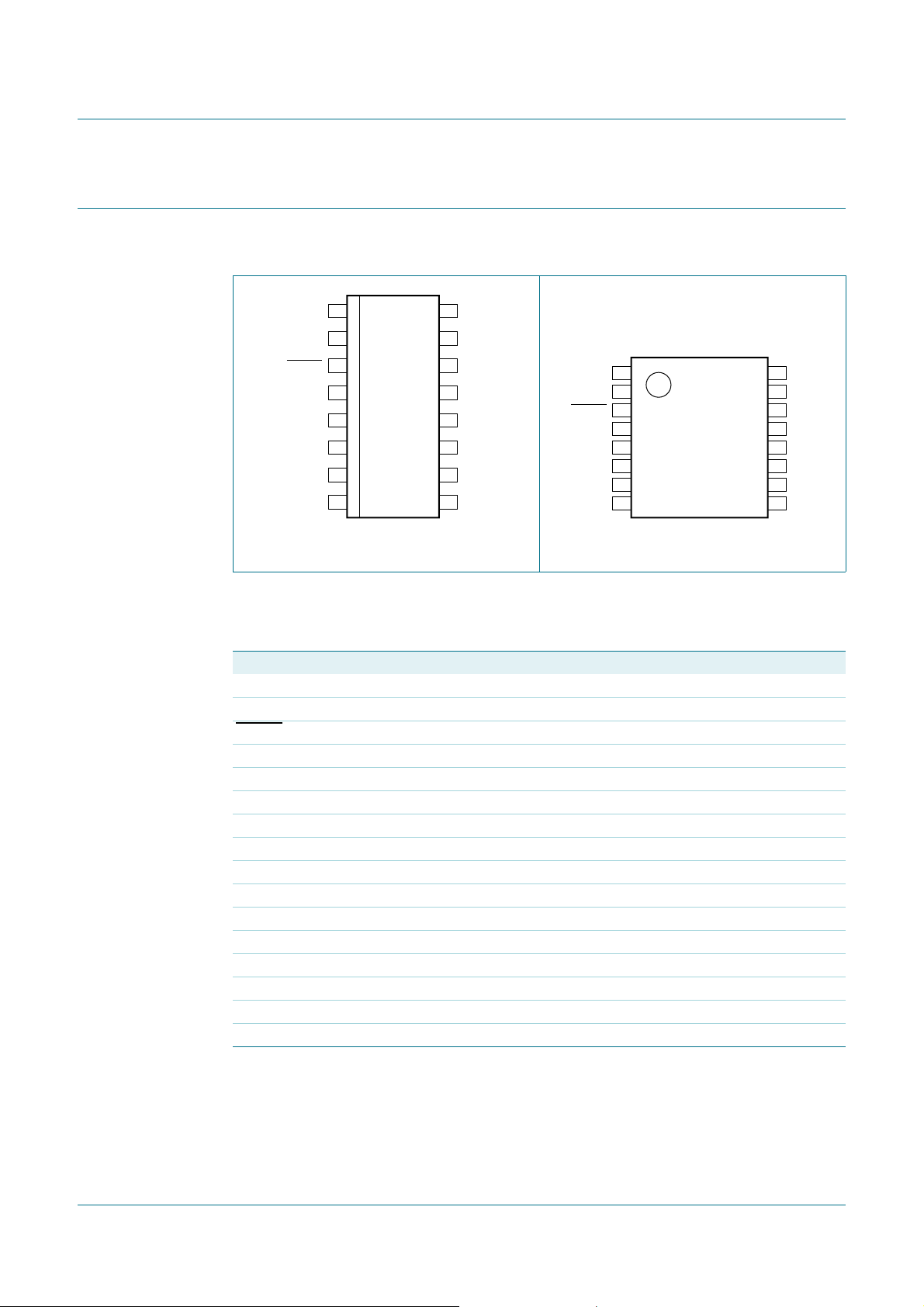
Package
Name Description Version
Table 1. Ordering information
Type number Topside
PCA9646D PCA9646 SO16 plastic small outline package; 16 leads; body width3.9 mm SOT109-1
PCA9646PW PCA9646 TSSOP16 plastic thin shrink small outline package; 16 leads;
SOT403-1
body width 4.4 mm
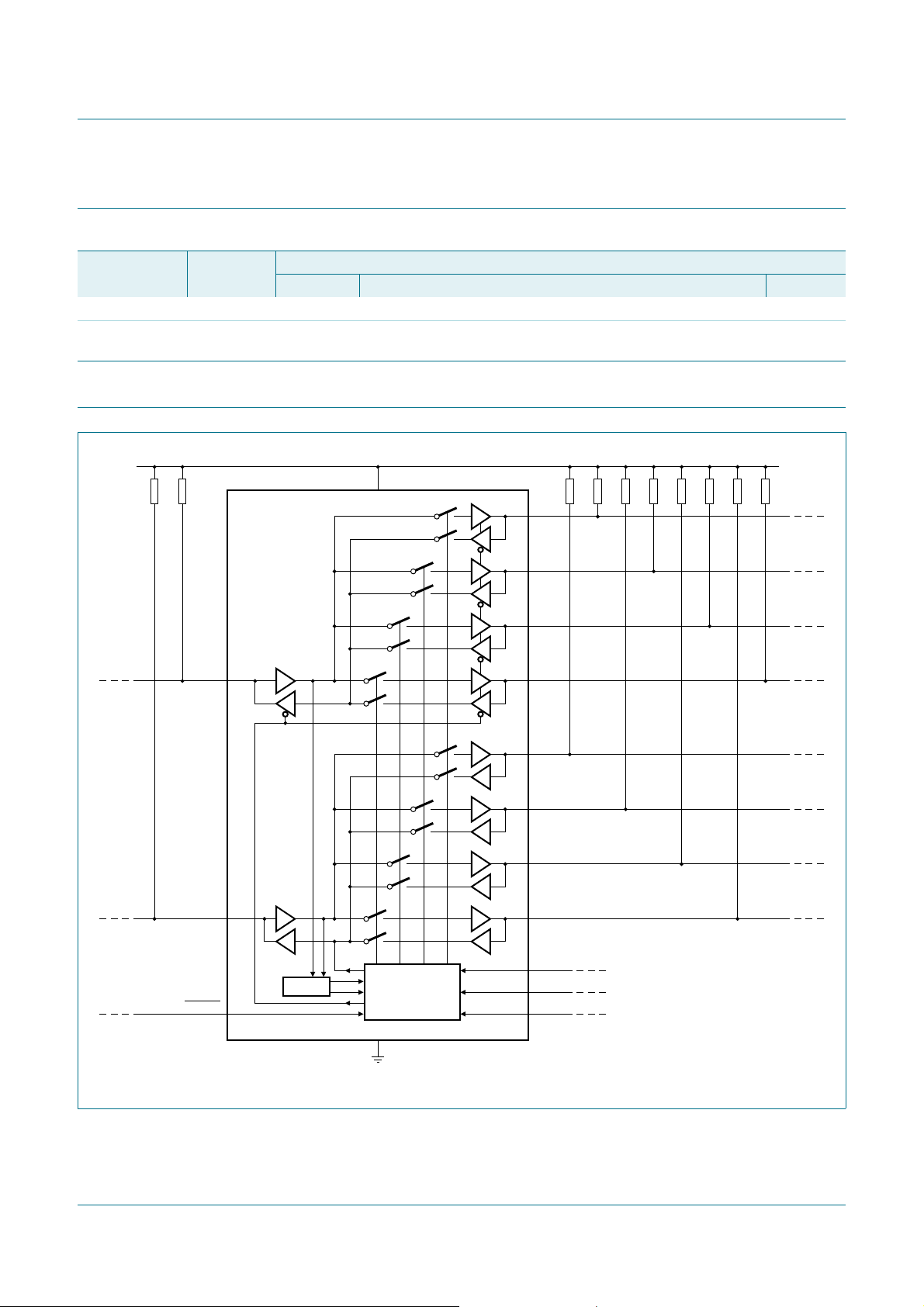
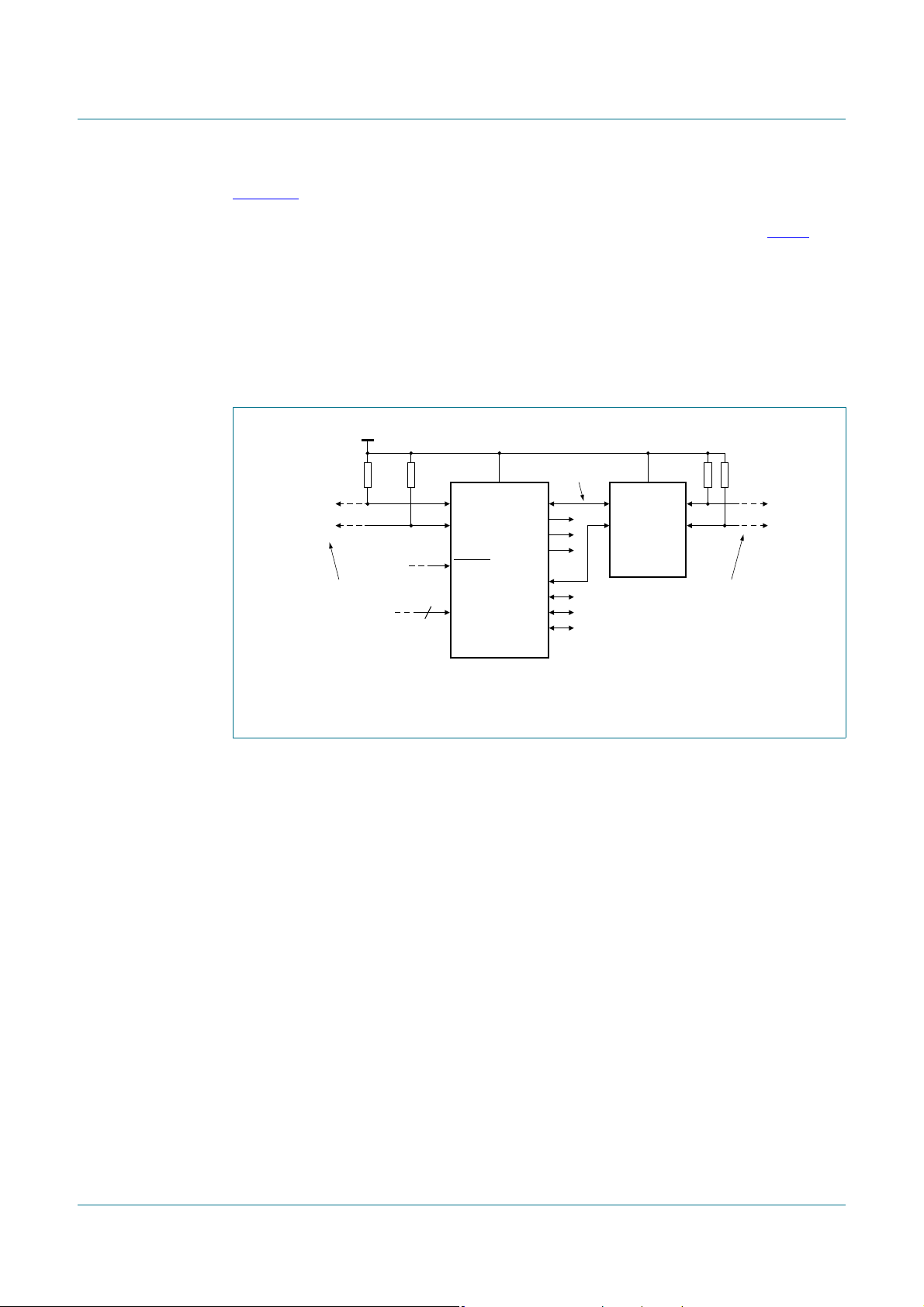
5. Block diagram
Fig 1. Simplified block diagram of PCA9646
PCA9646 All information provided in this document is subject to legal disclaimers. © NXP B.V. 2011. All rights reserved.
Product data sheet Rev. 1 — 1 March 2011 2 of 22
Page 3
NXP Semiconductors
PCA9646D
A0 V
DD
A1 SDA
RESET SCL
SD0 A2
SC0 SC3
SD1 SD3
SC1 SC2
V
SS
SD2
002aaf364
1
2
3
4
5
6
7
8
10
9
12
11
14
13
16
15
PCA9646PW
002aaf366
1
2
3
4
5
6
7
8
10
9
12
11
14
13
16
15
A0 V
DD
A1 SDA
RESET SCL
SD0 A2
SC0 SC3
SD1 SD3
SC1 SC2
V
SS
SD2
6. Pinning information
6.1 Pinning
PCA9646
Buffered 4-channel 2-wire bus switch
Fig 2. Pin configuration for SO16 Fig 3. Pin configuration for TSSOP16
6.2 Pin description
Table 2. Pin description
Symbol Pin Description
A0 1 address input 0
A1 2 address input 1
RESET
SD0 4 serial data 0
SC0 5 serial clock 0
SD1 6 serial data 1
SC1 7 serial clock 1
V
SS
SD2 9 serial data 2
SC2 10 serial clock 2
SD3 11 serial data 3
SC3 12 serial clock 3
A2 13 address input 2
SCL 14 serial clock line (normally input)
SDA 15 serial data line
V
DD
3 active LOW reset input
8 negative supply (ground)
16 positive supply
PCA9646 All information provided in this document is subject to legal disclaimers. © NXP B.V. 2011. All rights reserved.
Product data sheet Rev. 1 — 1 March 2011 3 of 22
Page 4

NXP Semiconductors
7. Functional description
Refer to Figure 1 “Simplified block diagram of PCA9646”.
7.1 VDD, VSS — DC supply pins
The power supply voltage for the PCA9646 may be any voltage in the range 2.7 V to
5.5 V. The IC supply must be common with the supply for the bus. Hysteresis on the port s
are a percentage of the IC’s power supply, hence noise margin considerations should be
taken into account when selecting an operating voltage.
7.2 SCL — clock signal input
The clock signal buffer is unidirectional, with this pin acting as the default input. However,
the clock signal direction may be reversed by setting the MSB of the Control register
HIGH. In normal I
signal to the slave. For lowest cost the PCA9646 combines unidirectional buffering of the
clock signal with a bidirectional buffer for the data signal. Clock stretching is therefore not
supported and slave devices that may require clock stretching must be accommodated by
the master adopting an appropriate clocking when communicating with them.
PCA9646
Buffered 4-channel 2-wire bus switch
2
C-bus operations the master device generates a unidirectional clock
The buffer includes hysteresis to ensure clean switching signals are output, especially
with slow rise times on high capacitively loaded buses.
7.3 SC0, SC1, SC2 , SC3 — clock signal outputs
The clock signal from SCL is buffered through four independent buffers, and the signal is
presented at the four SC0 to SC3 ports. Ports are open-drain type and require external
pull-up resistors.
When the MSB of the control register is set HIGH, the port direction is reversed. The
ANDed result of the selected SC0 to SC3 lines is then used to drive the open-dr ain output
of the SCL pin.
7.4 SDA, SD0, SD1, SD2, SD3 — data signal inputs/outputs
The data signal buffers are bidir ectional. The port ( SDA, or any one of SD0 to SD3) which
first falls LOW, will decide the direction of this buf fer and ‘lock out’ signals coming from the
opposite side. As the ‘input’ signal continues to fall, it will then drive the open-drain of the
‘output’ side LOW. Again, hysteresis is applied to the buffer to minimize the effects of
noise. Ports are open-drain type and require external pull-up resistors.
At some points during the communication, the data direction will reverse—for example,
when the slave transmits an acknowledge (ACK) or responds with its register contents.
During these times, the controlling ‘input’ side will have to rise to V
the ‘lock’, which then allows the ‘output’ side to gain control, and pull (what was) the ‘input’
side LOW again. This will cause a ‘pulse’ on the ‘input’ side, which can be quite long
duration in high capacitance buses. However, this pulse will not interfere with the actual
data transmission, as it should not occur during times of clock line transition (during
normal I
still met.
2
C-bus and SMBus protocols), and thus data signal set-up time requ irem ents are
before it releases
unlock
PCA9646 All information provided in this document is subject to legal disclaimers. © NXP B.V. 2011. All rights reserved.
Product data sheet Rev. 1 — 1 March 2011 4 of 22
Page 5
NXP Semiconductors
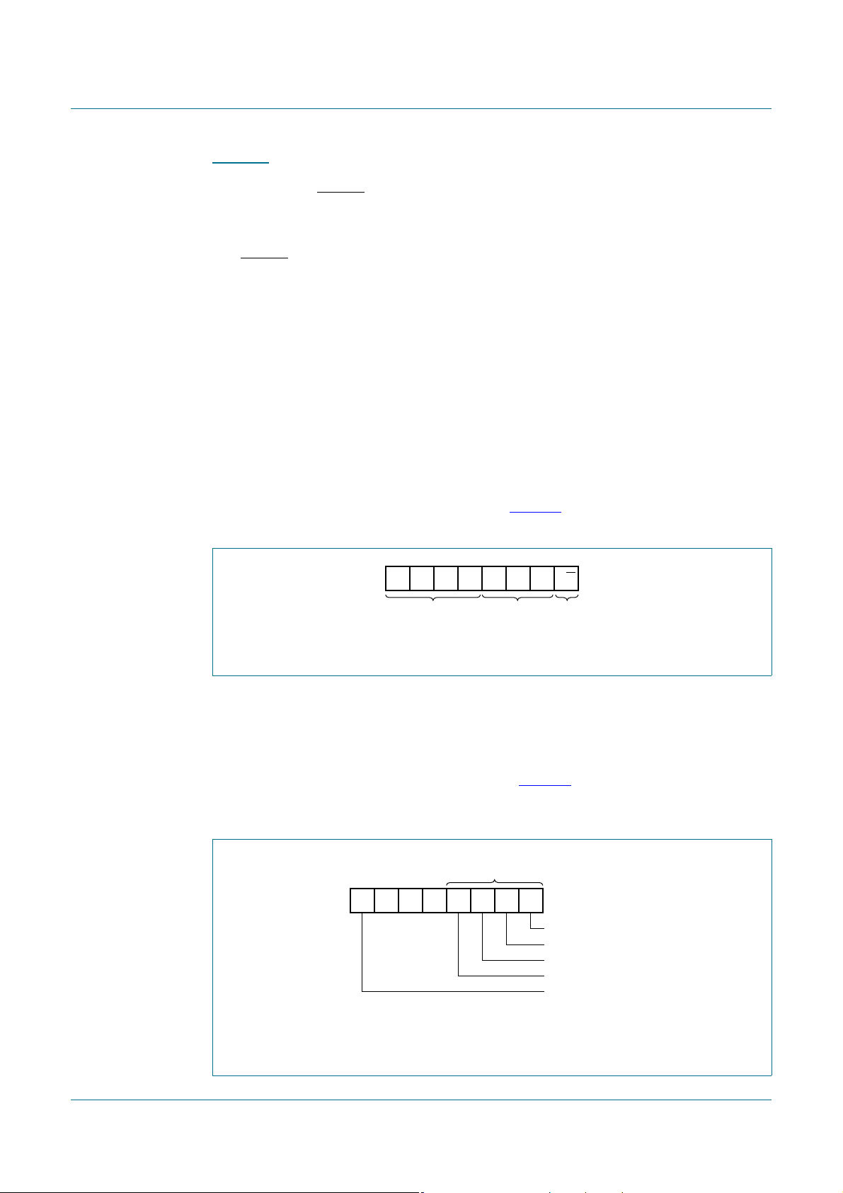
002aaf368
1 1 1 0 A2 A1 A0 R/W
fixed externally
selectable
read = 1
write = 0
002aaf369
B7 X X X B3 B2 B1 B0
output channel
enable bits
MSB LSB
SCL direction
0: SCL → SC0 to SC3
1: SC0 to SC3 → SCL
SC0/SD0 enable
SC1/SD1 enable
SC2/SD2 enable
SC3/SD3 enable
7.5 RESET — reset IC to default state
The active LOW RESET input is used to disable the buffer, and reset it to its default state.
The IC should only be disabled when the bus is idle to avoid truncation of commands
which may confuse other devices on the bus.
PCA9646
Buffered 4-channel 2-wire bus switch
The RESET
disabling all output lines SC[0:3] and SD[0:3]. It is the nature of the I
signal will clear the contents of the Control register, which has the effect of
2
C-bus protocol that
devices may become ‘stuck’. T o help in the clearin g of this condition, the PCA9646 can be
reset, and each port brought on-line successively to find the component holding the bus
LOW.
7.6 Power-On Reset (POR)
During power-on, the PCA9646 is internally held in the reset condition for a maximum of
t
= 500 ns. The default condition after reset is for the Control register to be erased
rst
(all zeros), resulting in all output channels being disabled.
7.7 A0, A1, A2 — address lines
The slave address of the PCA9646 is shown in Figure 4. The address pins (A2, A1, A0)
must be driven to a HIGH or LOW level—they are not internally pulled to a default state.
Fig 4. Slave address
The read/write bit must be set LOW to enable a write to the Control register, or HIGH to
read from the Control register.
7.8 Control register
The Control register of the PCA9646 is shown in Figure 5. Each of the four output
channels (SCn/SDn pairs) can be enabled independently, and the direction of the clock
signal can be reversed.
PCA9646 All information provided in this document is subject to legal disclaimers. © NXP B.V. 2011. All rights reserved.
Product data sheet Rev. 1 — 1 March 2011 5 of 22
Fig 5. Control register
Page 6
NXP Semiconductors
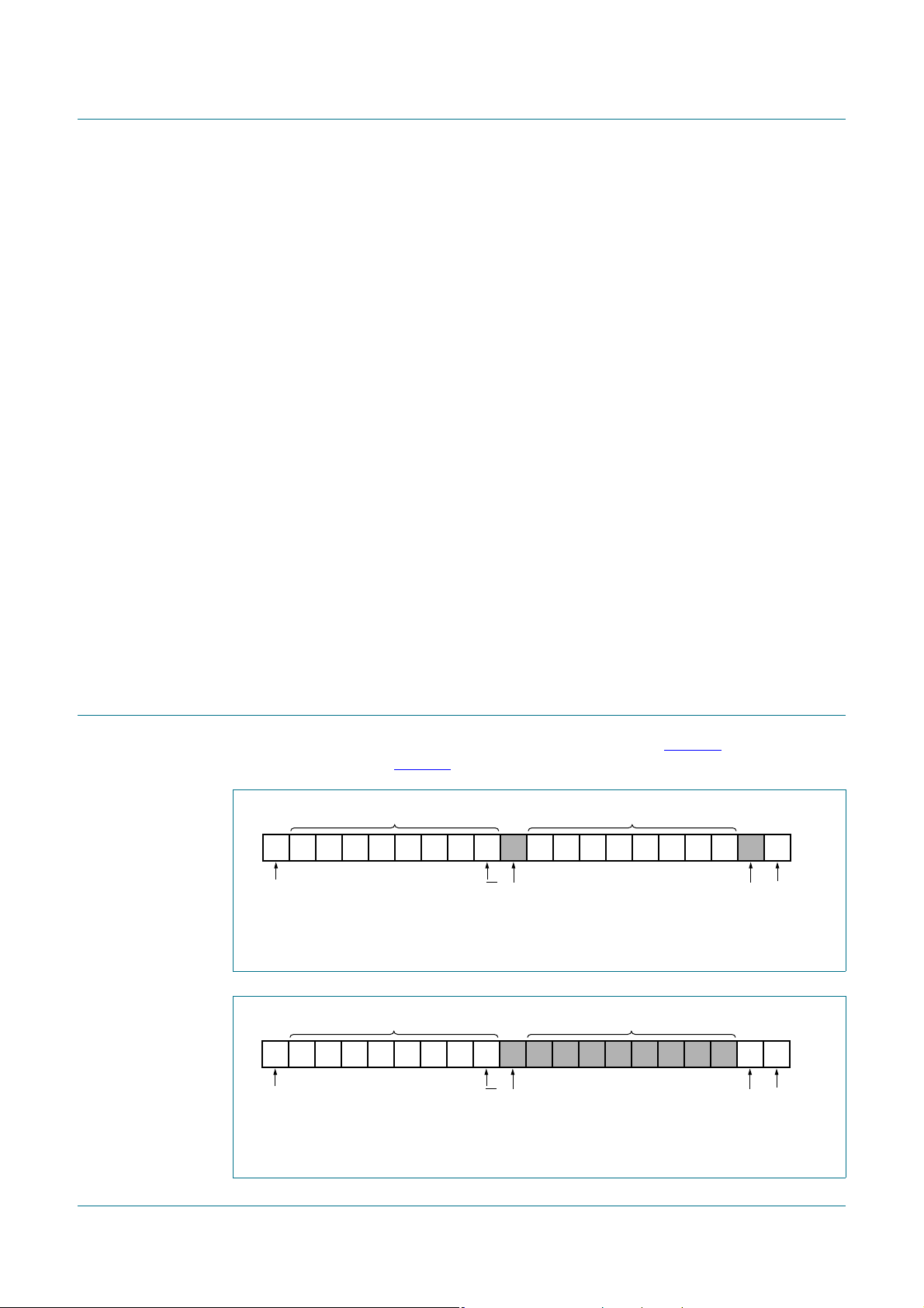
002aaf370
S 1 1 1 0 A2 A1 A0
slave address
0 A B7 X X X B3 B2 B1 B0 A P
Control register
START
condition
R/W acknowledge
from slave
acknowledge
from slave
STOP
condition
002aaf371
S 1 1 1 0 A2 A1 A0
slave address
1 A B7 0 0 0 B3 B2 B1 B0 NA P
Control register
START
condition
R/W acknowledge
from slave
not acknowledge
from master
STOP
condition
A LOW or ‘zero’ bit (B[3:0]) indicates that the respective channel (SC[3:0], SD[3:0]) is
disabled. The default reset condition of the register is all zeros, all channels disabled,
forward direction. A HIGH or ‘one’ bit indicates the respective channel is enabled.
Example: B3 = 1, B2 = 0, B1 = 1, B0 = 0 means channel 3 (SC3/SD3) and channel 1
(SC1/SD1) are enabled, and channel 2 (SC2/SD2) and channel 0 (SC0/SD0) are
disabled.
As each channel is individually buffered, the loads on each are isolated, and therefore
there is no special requirement to keep the sum of the collective capacitances below the
maximum bus capacitance. Instead, each line may have up to the maximum bus
capacitance and be enabled or disabled without affecting the performance of the other
channels.
The Most Significant Bit (MSB) B7 is used to set the direction of the SCL (clock) signal.
The default state is LOW (zero). In this state, the SCL port will act as the input, and the IC
will supply a buffered signal to any of the four output channels (SC0 to SC3) which are
enabled. When B7 is set HIGH (one), the clock signal direction is reversed. The ports
SC0 to SC3 act as inputs, the ANDed combination of the selected signals is buffered and
output on the SCL pin.
PCA9646
Buffered 4-channel 2-wire bus switch
The PCA9646 is always addressable from the SCL/SDA side, regardless of the state of
B7. Any device which can communicate data to the SCL/SDA pins, either by being directly
attached to those pins or by transmitting through the PCA9646 (when B7 = 1), may
address the device and change the control register’s contents. The Control register is only
updated upon receipt of the STOP condition.
8. Bus transaction
A typical I2C-bus write transaction to the PCA9646 is shown in Figure 6. A typical read
transaction is shown in Figure 7
Fig 6. PCA9646 write transaction to Control register
.
PCA9646 All information provided in this document is subject to legal disclaimers. © NXP B.V. 2011. All rights reserved.
Product data sheet Rev. 1 — 1 March 2011 6 of 22
Fig 7. PCA9646 read transaction from Control register
Page 7
NXP Semiconductors
9. Limiting values
PCA9646
Buffered 4-channel 2-wire bus switch
Table 3. Limiting values
In accordance with the Absolute Maximum Rating System (IEC 60134).
Symbol Parameter Conditions Min Max Unit
V
DD
V
I/O
V
I
supply voltage
voltage on an input/output pin pins SDx, SCx
input voltage RESET pin
address pins A2, A1, A0
I
I
input current pins other than SCx/SDx - 20 mA
[1]
0.3 +7 V
[1]
VSS 0.5 +7 V
[1]
VSS 0.5 VDD+0.5 V
[1]
VSS 0.5 VDD+0.5 V
all SCx and SDx - 40 mA
I
SS
P
tot
T
stg
T
amb
[1] Voltages are specified with respect to pin 8 (VSS).
ground supply current - 280 mA
total power dissipation - 300 mW
storage temperature 55 +125 C
ambient temperature operating 40 +85 C
10. Characteristics
Table 4. Characteristics
=40C to +85C; voltages are specified with respect to ground (VSS); VDD= 5.5 V unl ess oth erwise specified.
T
amb
Symbol Parameter Conditions Min Typ Max Unit
Power supply
V
DD
I
DD
2
C-bus ports (SCL, SDA, SC[3:0], SD[3:0])
I
V
I2C-bus
V
IL
V
IH
V
I(hys)
I
LI
I
O(sink)
V
OL
supply voltage operating 2.7 - 5.5 V
supply current quiescent; VI(RESET pin)=0V--1 A
I2C-bus voltage SDx, SCx - - 5.5 V
LOW-level input voltage VDD=2.7V
HIGH-level input voltage VDD=2.7V
hysteresis of input voltage VDD=2.7V
input leakage current pin at VDDor V
output sink current LOW-level; V
LOW-level output voltage IOL=30mA; VDD= 2.7 V - 260 450 mV
Pins SDA, SD0, SD1, SD2, SD3
V
V
lock
unlock
direction lock voltage VDD=2.7V
direction unlock voltage VDD=2.7V
[1]
--0.4V
=5.5V
V
DD
=5.5V
V
DD
=5.5V
V
DD
SS
input < V
Sxx
=30mA; VDD= 5.5 V - 140 275 mV
I
OL
=5.5V
V
DD
=5.5V
V
DD
IL
[1]
--0.5V
[1]
1.2 - - V
[1]
2.0 - - V
[1]
80 - - mV
[1]
200 - - mV
1- +1 A
30 - - mA
[1]
--1.3V
[1]
--3.0V
[1]
2.0 - - V
[1]
4.8 - - V
PCA9646 All information provided in this document is subject to legal disclaimers. © NXP B.V. 2011. All rights reserved.
Product data sheet Rev. 1 — 1 March 2011 7 of 22
Page 8
NXP Semiconductors
002aaf438
t
f
t
d
V
I2C-bus
time
70 % V
DD
30 % V
DD
SDx, SCx input
SDx, SCx output
V
IL
PCA9646
Buffered 4-channel 2-wire bus switch
Table 4. Characteristics
T
=40C to +85C; voltages are specified with respect to ground (VSS); VDD= 5.5 V unl ess oth erwise specified.
amb
…continued
Symbol Parameter Conditions Min Typ Max Unit
RESET
V
IH
V
IL
V
hys
I
LI
t
w(rst)L
t
rst
t
POR
HIGH-level input voltage VDD= 2.7 V 2.0 - - V
= 5.5 V 4.8 - - V
V
DD
LOW-level input voltage VDD= 2.7 V - - 650 mV
= 5.5 V - - 900 mV
V
DD
hysteresis voltage VDD=2.7V 100 - - mV
=5.5V 200 - - mV
V
DD
input leakage current pin at VDDor V
LOW-level reset time VI<V
IL
SS
reset time RESET pin; from VI > V
power-on reset pulse time RESET pin; from VI > V
IH
IH
1- +1 A
[2]
-25- ns
- 250 500 ns
- 250 500 ns
Address pins (A0, A1, A2)
V
IH
V
IL
I
LI
Timing characteristics (Figure 8
t
d
t
f
HIGH-level input voltage VDD= 2.7 V 1.7 - - V
= 5.5 V 3.5 - - V
V
DD
LOW-level input voltage VDD=2.7V --0.7V
=5.5V --1.5V
V
DD
input leakage current pin at VDDor V
SS
1- +1 A
)
delay time RPU = 200 ; VDD= 2.7 V - 100 - ns
= 200 ; VDD=5.5V - 70 - ns
R
PU
fall time RPU = 200 -16- ns
[1] Supply voltage dependent; refer to graphs (Figure 9 through Figure 12) for typical trend.
[2] Guaranteed by design, not subject to test.
Fig 8. Timing diagram
PCA9646 All information provided in this document is subject to legal disclaimers. © NXP B.V. 2011. All rights reserved.
Product data sheet Rev. 1 — 1 March 2011 8 of 22
Page 9

NXP Semiconductors
2
3
1
4
5
V
I
(V)
0
V
DD
(V)
26534
002aaf333
V
lock
V
IH
V
IL
400
600
200
800
1000
V
I(hys)
(V)
0
V
DD
(V)
26534
002aaf334
T
amb
= +85 °C
+25 °C
−40 °C
100
150
50
200
250
V
OL
(mV)
0
R
PU
(Ω)
0 1000800400 600200
002aaf372
VDD = 5.5 V
2.7 V
100
300
400
V
OL
(mV)
0
T
amb
(C)
−50 150100050
002aaf373
200
VDD = 2.7 V
5.5 V
PCA9646
Buffered 4-channel 2-wire bus switch
T
=25C
amb
Fig 9. Typical input levels versus supply voltage Fig 10. Typical VIH VIL hysteresis versus supply
voltage
Fig 11. Typical LOW-level output voltage versus
PCA9646 All information provided in this document is subject to legal disclaimers. © NXP B.V. 2011. All rights reserved.
Product data sheet Rev. 1 — 1 March 2011 9 of 22
T
=25CI
amb
=30mA
OL
Fig 12. Typical LOW-level output voltage versus
pull-up resistance
ambient temperature
Page 10
NXP Semiconductors
002aaf374
S
START
sequence
SCL
(clock)
SDA
(data)
A0
(master)A1(master)A2(master)
master side of PCA9646
slave side of PCA9646
purpose of bit (address bit 5)
device asserting data line (master/slave)
A3
(master)
A4
(master)A5(master)
A6
(master)
SDA direction
'hand over' pulses upon change
of device asserting the data line
W
(master)
ACK
(slave)
P
STOP
sequence
11. Application information
Figure 13 shows a typical data transfer through the PCA9646. The PCA9646 has
excellent application to extending loads and expanding the address space of slave
devices. Rise times are determined simply by the side of the buffer with the slowest RC
time constant.
PCA9646
Buffered 4-channel 2-wire bus switch
Remark: Input to output delay exaggerated for clarity.
Fig 13. Typical communication sequence through the PCA9646
Figure 14 shows a typical application for the PCA9646. Each channel can support up to
the maximum permissible capacitance load, thus the maximum loading of the system can
be 5 times that which could be achieved without buffering.
The channel enable function can be used to interface buses of different operating
frequencies. When certain bus sections are enabled, the system frequency may be limited
by a bus section having a slave device specified only to 100 kHz. When that bus section is
disabled, the slow slave is isolated and the remaining bus can be run at 400 kHz. The
timing performance and current sinking capability will allow the PCA9646 to run in excess
2
of the 1 MHz maximum limit of the I
C-bus Fast-mode Plus (Fm+), or to run a huge 4 nF
load at 100 kHz.
Figure 15
shows the PCA9646 used as a line driver . Fou r such lines (only one shown) can
be run from the same device. The receiving end may then again be used as a 4-way bus
switch, radiating out into another four lines.
Using the address pins, this entire structure may be repeated. Thus a total of eight
PCA9646 ‘line drivers’ may be connected to a single bus master (U1), allowing for
32 (8 4) long distance bus pairs to be driven from the one I
2
C-bus port.
PCA9646 All information provided in this document is subject to legal disclaimers. © NXP B.V. 2011. All rights reserved.
Product data sheet Rev. 1 — 1 March 2011 10 of 22
Page 11
NXP Semiconductors
002aaf375
BUS MASTER
U3
V
DD
SCL
SDA
R8
1.1 kΩ
SC0
SD0
SCL
SDA
PCA9646
V
DD
SC0
SD0
U1
RESET
3.3 V
SCL
SDA
V
DD
MASTER/
SLAVE
U4
SCL
SDA
V
DD
SLAVE
U5
SCL
SDA
V
DD
SLAVE
U6
R7
1.1 kΩ
R1
1.1 kΩ
R2
1.1 kΩ
SC2
SD2
SC2
SD2
R3
1.1 kΩR41.1 kΩ
SC3
SD3
SC3
SD3
R5
1.1 kΩR61.1 kΩ
400 pF load at 1 MHz
or 4 nF load at 100 kHz
400 pF load at 1 MHz
or 4 nF load at 100 kHz
400 pF load at 1 MHz
or 4 nF load at 100 kHz
A0
A1
A2
V
SS
R10
1.1 kΩ
SC1
SD1
SC1
SD1
SCL
SDA
V
DD
SLAVE
U7
SCL
SDA
V
DD
SLAVE
U8
R9
1.1 kΩ
400 pF load at 1 MHz
or 4 nF load at 100 kHz
400 pF load at 1 MHz
or 4 nF load at 100 kHz
002aaf376
BUS
MASTER
U1
V
DD
SCL
SDA
R4
180 Ω
SCL
SDA
PCA9646
V
DD
SC0
SC1
U2
RESET
5 V
R3
180 Ω
R1 R2
A0
A1
e.g., PC/TV
receiver or
decoder box
SD0
SD1
etc.
SC2
SC3
A2
SD2
SD3
SCL
SDA
PCA9646
V
DD
SC0
SC1
U3
RESET
A0
A1
SD0
SD1
SC2
SC3
A2
SD2
SD3
address address
backplane or
long cable run
with 30 mA
pull-up current
SLAVE
U4
V
DD
SCL
SDA
R6R5
e.g., monitor,
flat TV, LED array
PCA9646
Buffered 4-channel 2-wire bus switch
Fig 14. PCA9646 typical buffer application
Fig 15. PCA9646 as a 30 mA line driver
PCA9646 All information provided in this document is subject to legal disclaimers. © NXP B.V. 2011. All rights reserved.
Product data sheet Rev. 1 — 1 March 2011 11 of 22
Page 12
NXP Semiconductors
002aaf377
SCL
SDA
SCL
SDA
PCA9646
V
DD
SC0
SC1
U1
RESET
5 V
R1
1.8 kΩR21.8 kΩ
A[2:0]
SD0
SD1
SC2
SC3
SD2
SD3
P82B715
U2
V
CC
SX
SY
R4R3
3
LX
LY
long cable runisolated I2C-bus
no pull-up
required
PCA9646
Buffered 4-channel 2-wire bus switch
Figure 16 shows how PCA9646 can be used to combine or extend existing long cable
systems using P82B715 I
capacitance limit. P82B715 alone provides a ‘10 impedance transformation’ (Ref. 2
2
C-bus extenders when they have reached their maximum
) but
no isolation of the loadings on either side. P82B715 systems have a finite capacitance
limit and its system calculations can be relatively complex. The buffering action of
PCA9646 simplifies calculations and allows the isolated bus rise time to meet the
Fast-mode requirement even when that is not possible on the long cable section.
Of course it is possible to create a much larger system by connecting existing long
P82B715 cable systems to each of the four channels and driving all of them from one
isolated Master.
PCA9646 provides bus isolation and simplifies calculation of bus RC components.
Fig 16. PCA9646 isolating the standard I2C-bus from a P82B715 used as a line driver
PCA9646 All information provided in this document is subject to legal disclaimers. © NXP B.V. 2011. All rights reserved.
Product data sheet Rev. 1 — 1 March 2011 12 of 22
Page 13
NXP Semiconductors
002aaf378
SCL
SCL
SDA
PCA9646
V
DD
SC0
SC1
U2
RESET
5 V
R1
180 ΩR2180 Ω
A[2:0]
SD0
SD1
SC2
SC3
SD2
SD3
3
BUS
MASTER
U1
V
DD
SCL
SDA
000b
up to seven PCA9646s
on each output pair
(address: 001b to 111b)
structure in
dashed box
repeated
etc.
R4
180 Ω
R3
180 Ω
SCL
SDA
PCA9646
V
DD
SC0
SC1
U3
RESET
SD0
SD1
SC2
SC3
SD2
SD3
A[2:0]
3
001b
total output of
4 × 7 × 4 = 112
individually enabled
fully isolated buses,
each with full
capacitance load
(e.g., 400 pF at 1 MHz)
5 V
SCL
SDA
PCA9646
V
DD
SC0
SC1
U4
RESET
SD0
SD1
SC2
SC3
SD2
SD3
A[2:0]
3
010b
connect, for example,
8 LED driver ICs,
each with 8 LED
outputs = 7168 LEDs
up to seven devices
(address: 001b to 111b)
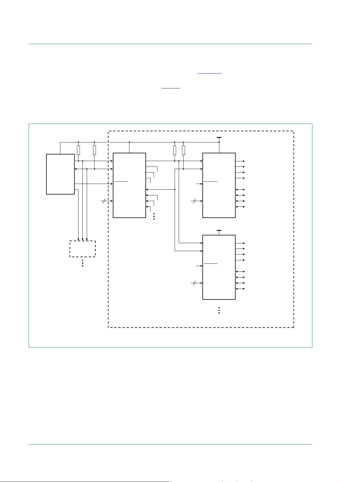
The PCA9646 may also be driven in series. Figure 17 shows this configuration. In this
scenario, each of the four outputs of the first device (U2) has six more PCA9646’s
connected to it. Each of those six devices has four outputs, thus giving
4 7 4 = 112 outputs. If the RESET
be possible to reproduce this entire structure multiple times, giving a truly massive
address space capability. Such a configuration may be applied to situations such as
display drivers.
PCA9646
Buffered 4-channel 2-wire bus switch
pin on U2 was also driven from the master, it would
Fig 17. PCA9646 series implementation for large I/O fan-out
PCA9646 All information provided in this document is subject to legal disclaimers. © NXP B.V. 2011. All rights reserved.
Product data sheet Rev. 1 — 1 March 2011 13 of 22
Page 14

NXP Semiconductors
X
w M
θ
A
A
1
A
2
b
p
D
H
E
L
p
Q
detail X
E
Z
e
c
L
v M
A
(A )
3
A
8
9
1
16
y
pin 1 index
UNIT
A
max.
A
1
A2A3b
p
cD
(1)E(1) (1)
eHELLpQZywv θ
REFERENCES
OUTLINE
VERSION
EUROPEAN
PROJECTION
ISSUE DATE
IEC JEDEC JEITA
mm
inches
1.75
0.25
0.10
1.45
1.25
0.25
0.49
0.36
0.25
0.19
10.0
9.8
4.0
3.8
1.27
6.2
5.8
0.7
0.6
0.7
0.3
8
0
o
o
0.25 0.1
DIMENSIONS (inch dimensions are derived from the original mm dimensions)
Note
1. Plastic or metal protrusions of 0.15 mm (0.006 inch) maximum per side are not included.
1.0
0.4
SOT109-1
99-12-27
03-02-19
076E07 MS-012
0.069
0.010
0.004
0.057
0.049
0.01
0.019
0.014
0.0100
0.0075
0.39
0.38
0.16
0.15
0.05
1.05
0.041
0.244
0.228
0.028
0.020
0.028
0.012
0.01
0.25
0.01 0.004
0.039
0.016
0 2.5 5 mm
scale
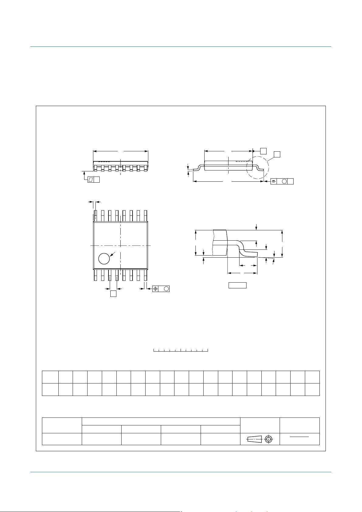
SO16: plastic small outline package; 16 leads; body width 3.9 mm
SOT109-1
12. Package outline
PCA9646
Buffered 4-channel 2-wire bus switch
Fig 18. Package outline SOT109-1 (SO16)
PCA9646 All information provided in this document is subject to legal disclaimers. © NXP B.V. 2011. All rights reserved.
Product data sheet Rev. 1 — 1 March 2011 14 of 22
Page 15
NXP Semiconductors
UNIT A1A2A3b
p
cD
(1)E(2) (1)
eHELLpQZywv θ
REFERENCES
OUTLINE
VERSION
EUROPEAN
PROJECTION
ISSUE DATE
IEC JEDEC JEITA
mm
0.15
0.05
0.95
0.80
0.30
0.19
0.2
0.1
5.1
4.9
4.5
4.3
0.65
6.6
6.2
0.4
0.3
0.40
0.06
8
0
o
o
0.13 0.10.21
DIMENSIONS (mm are the original dimensions)
Notes
1. Plastic or metal protrusions of 0.15 mm maximum per side are not included.
2. Plastic interlead protrusions of 0.25 mm maximum per side are not included.
0.75
0.50
SOT403-1 MO-153
99-12-27
03-02-18
w M
b
p
D
Z
e
0.25
18
16
9
θ
A
A
1
A
2
L
p
Q
detail X
L
(A )
3
H
E
E
c
v M
A
X
A
y
0 2.5 5 mm
scale
TSSOP16: plastic thin shrink small outline package; 16 leads; body width 4.4 mm
SOT403-1
A
max.
1.1
pin 1 index
PCA9646
Buffered 4-channel 2-wire bus switch
Fig 19. Package outline SOT403-1 (TSSOP16)
PCA9646 All information provided in this document is subject to legal disclaimers. © NXP B.V. 2011. All rights reserved.
Product data sheet Rev. 1 — 1 March 2011 15 of 22
Page 16

NXP Semiconductors
13. Handling information
CAUTION
This device is sensitive to ElectroStatic Discharge (ESD). Observe precautions for handling
electrostatic sensitive devices.
Such precautions are described in the ANSI/ESD S20.20, IEC/ST 61340-5, JESD625-A or
equivalent standards.
14. Soldering of SMD packages
This text provides a very brief insight into a complex technology . A more in-depth account
of soldering ICs can be found in Application Note AN10365 “Surface mount reflow
soldering description”.
14.1 Introduction to soldering
Soldering is one of the most common methods through which packages are attached to
Printed Circuit Boards (PCBs), to form electrical circuits. The soldered joint provides both
the mechanical and the electrical connection. There is no single soldering method that is
ideal for all IC packages. Wave soldering is often preferred when through-hole and
Surface Mount Devices (SMDs) are mixed on one printed wiring board; however, it is not
suitable for fine pitch SMDs. Reflow soldering is ideal for the small pitches and high
densities that come with increased miniaturization.
PCA9646
Buffered 4-channel 2-wire bus switch
14.2 Wave and reflow soldering
Wave soldering is a joining technology in which the joints are made by solder coming from
a standing wave of liquid solder. The wave soldering process is suitable for the following:
• Through-hole components
• Leaded or leadless SMDs, which are glued to the surface of the printed circuit board
Not all SMDs can be wave soldered. Packages with solder balls, and some leadless
packages which have solder lands underneath the body, cannot be wave soldered. Also,
leaded SMDs with leads having a pitch smaller than ~0.6 mm cannot be wave soldered,
due to an increased probability of bridging.
The reflow soldering process involves applying solder paste to a board, followed by
component placement and exposure to a temperature profile. Leaded packages,
packages with solder balls, and leadless packages are all reflow solderable.
Key characteristics in both wave and reflow soldering are:
• Board specifications, including the board finish, solder masks and vias
• Package footprints, including solder thieves and orientation
• The moisture sensitivity level of the packages
• Package placement
• Inspection and repair
• Lead-free soldering versus SnPb soldering
PCA9646 All information provided in this document is subject to legal disclaimers. © NXP B.V. 2011. All rights reserved.
Product data sheet Rev. 1 — 1 March 2011 16 of 22
Page 17

NXP Semiconductors
14.3 Wave soldering
Key characteristics in wave soldering are:
• Process issues, such as application of adhesive and flux, clinching of leads, board
• Solder bath specifications, including temperature and impurities
14.4 Reflow soldering
Key characteristics in reflow soldering are:
• L ead-free versus SnPb sold ering; note that a lead-fr ee reflow process usually leads to
• Solder paste printing issues including smearing, release, and adjusting the process
• Reflow temperature profile; this profile includes preheat, reflow (in which the board is
Table 5. SnPb eutectic process (from J-STD-020C)
Package thickness (mm) Package reflow temperature (C)
< 2.5 235 220
2.5 220 220
PCA9646
Buffered 4-channel 2-wire bus switch
transport, the solder wave parameters, and the time during which components are
exposed to the wave
higher minimum peak temperatures (see Figure 20
reducing the process window
window for a mix of large and small components on one board
heated to the peak temperature) and cooling down. It is imperative that the peak
temperature is high enough for the solder to make reliable solder joint s (a solder paste
characteristic). In addition, the peak temperature must be low enough that the
packages and/or boards are not damaged. The peak temperature of the package
depends on package thickness and volume and is classified in accordance with
Table 5
and 6
Volume (mm3)
< 350 350
) than a SnPb process, thus
Table 6. Lead-free process (from J-STD-020C)
Package thickness (mm) Package reflow temperature (C)
Volume (mm3)
< 350 350 to 2000 > 2000
< 1.6 260 260 260
1.6 to 2.5 260 250 245
> 2.5 250 245 245
Moisture sensitivity precautions, as indicated on the packing, must be respected at all
times.
Studies have shown that small packages reach higher temperatures during reflow
soldering, see Figure 20
PCA9646 All information provided in this document is subject to legal disclaimers. © NXP B.V. 2011. All rights reserved.
Product data sheet Rev. 1 — 1 March 2011 17 of 22
.
Page 18

NXP Semiconductors
001aac844
temperature
time
minimum peak temperature
= minimum soldering temperature
maximum peak temperature
= MSL limit, damage level
peak
temperature
Fig 20. Temperature profiles for large and small components
PCA9646
Buffered 4-channel 2-wire bus switch
MSL: Moisture Sensitivity Level
For further information on temperature profiles, refer to Application Note AN10365
“Surface mount reflow soldering description”.
15. Abbreviations
Table 7. Abbreviations
Acronym Description
CMOS Complementary Metal-Oxide Semiconductor
2
C-bus Inter-Integrated Circuit bus
I
I/O Input/Output
IC Integrated Circuit
LED Light-Emitting Diode
MSB Most Significant Bit
PMBus Power Management Bus
RAID Redundant Array of Independent Discs
RC Resistor-Capacitor network
SMBus System Management Bus
16. References
[1] UM10204, “I2C-bus specification and user manual” — NXP Semiconductors;
[2] P82B715, I2C-bus extender — NXP Semiconducto rs; Product data sheet;
www.nxp.com/documents/user_manual/UM10204.pdf
www.nxp.com/documents/data_sheet/P82B715.pdf
PCA9646 All information provided in this document is subject to legal disclaimers. © NXP B.V. 2011. All rights reserved.
Product data sheet Rev. 1 — 1 March 2011 18 of 22
Page 19

NXP Semiconductors
PCA9646
Buffered 4-channel 2-wire bus switch
17. Revision history
Table 8. Revision history
Document ID Release date Data sheet status Change notice Supersedes
PCA9646 v.1 20110301 Product data sheet - -
PCA9646 All information provided in this document is subject to legal disclaimers. © NXP B.V. 2011. All rights reserved.
Product data sheet Rev. 1 — 1 March 2011 19 of 22
Page 20

NXP Semiconductors
PCA9646
Buffered 4-channel 2-wire bus switch
18. Legal information
18.1 Data sheet status
Document status
Objective [short] data sheet Development This document contains data from the objective specification for product development.
Preliminary [short] data sheet Qualification This document contains data from the preliminary specification.
Product [short] data sheet Production This document contains the product specification.
[1] Please consult the most recently issued document before initiating or completing a design.
[2] The term ‘short data sheet’ is explained in section “Definitions”.
[3] The product status of device(s) d escribed i n this docu ment may have changed si nce this d ocument was p ublished and may dif fer in case of multiple devices. The latest product statu s
information is available on the Internet at URL http://www.nxp.com.
[1][2]
Product status
[3]
Definition
18.2 Definitions
Draft — The document is a draft version only. The content is still under
internal review and subject to formal approval, which may result in
modifications or additions. NXP Semiconductors does not give any
representations or warranties as to the accuracy or completeness of
information included herein and shall have no liability for the consequences of
use of such information.
Short data sheet — A short data sheet is an extract from a full data sheet
with the same product type number(s) and title. A short data sheet is intended
for quick reference only and should not be relied upon to co nt ain det ailed and
full information. For detailed and full information see the relevant full data
sheet, which is available on request via the local NXP Semiconductors sales
office. In case of any inconsistency or conflict with the short data sheet, the
full data sheet shall prevail.
Product specification — The information and data provided in a Product
data sheet shall define the specification of the product as agreed between
NXP Semiconductors and its customer, unless NXP Semiconductors and
customer have explicitly agreed otherwise in writing. In no event however,
shall an agreement be valid in which the NXP Semiconductors product is
deemed to offer functions and qualities beyond those described in the
Product data sheet.
18.3 Disclaimers
Limited warranty and liability — Information in this document is believed to
be accurate and reliable. However, NXP Semiconductors does not give any
representations or warranties, expressed or implied, as to the accuracy or
completeness of such information and shall have no liability for the
consequences of use of such information.
In no event shall NXP Semiconductors be liable for any indirect, incidental,
punitive, special or consequential damages (including - without limitation - lost
profits, lost savings, business interruption, costs related to the removal or
replacement of any products or rework charges) whether or not such
damages are based on tort (including negligence), warranty, breach of
contract or any other legal theory.
Notwithstanding any damages that customer might incur for any reason
whatsoever, NXP Semi conductors’ aggregat e and cumulative liabil ity towards
customer for the products described herein shall be limited in accordance
with the Terms and conditions of commercial sale of NXP Semiconductors.
Right to make changes — NXP Semiconductors reserves the right to make
changes to information published in this document, including without
limitation specifications and product descriptions, at any time and without
notice. This document supersedes and replaces all information supplied prior
to the publication hereof.
Suitability for use — NXP Semiconductors products are not designed,
authorized or warranted to be suitable for use in life support, life-critical or
safety-critical systems or equipment, nor in applications where failure or
malfunction of an NXP Semiconductors product can reasonably be expected
to result in personal injury, death or severe property or environmental
damage. NXP Semiconductors accepts no liability for inclusion and/or use of
NXP Semiconductors products in such equipment or applications and
therefore such inclusion and/or use is at the customer’s own risk.
Applications — Applications that are described herein for any of these
products are for illustrative purposes only. NXP Semiconductors makes no
representation or warranty that such applications will be suitable for the
specified use without further testing or modification.
Customers are responsible for the design and operation of their applications
and products using NXP Semiconductors products, and NXP Semiconductors
accepts no liability for any assistance with applications or customer product
design. It is customer’s sole responsibility to determine whether the NXP
Semiconductors product is suitable and fit for the customer’s applications and
products planned, as well as for the planned application and use of
customer’s third party customer(s). Customers should provide appropriate
design and operating safeguards to minimize the risks associated with their
applications and products.
NXP Semiconductors does not accept any liability related to any default ,
damage, costs or problem which is based on any weakness or default in the
customer’s applications or products, or the application or use by customer’s
third party customer(s). Customer is responsible for doing all necessary
testing for the customer’s applications and products using NXP
Semiconductors products in order to avoid a default of the applications and
the products or of the application or use by customer’s third part y
customer(s). NXP does not accept any liability in this respect.
Limiting values — Stress above one or more limiting values (as defined in
the Absolute Maximum Ratings System of IEC 60134) will cause permanent
damage to the device. Limiting values are stress ratings only and (proper)
operation of the device at these or any other conditions above those given in
the Recommended operating conditions section (if present) or the
Characteristics sections of this document is not warranted. Constant or
repeated exposure to limiting values will permanently and irreversibly affect
the quality and reliability of the device.
Terms and conditions of commercial sale — NXP Semiconductors
products are sold subject to the general terms and conditions of commercial
sale, as published at http://www.nxp.com/profile/terms
agreed in a valid written individual agreement. In case an individual
agreement is concluded only the terms and conditions of the respective
agreement shall apply. NXP Semiconductors hereby expressly objects to
applying the customer’s general terms and conditions with regard to the
purchase of NXP Semiconductors products by customer.
No offer to sell or license — Nothing in this document may be interpreted or
construed as an offer to sell product s that is open for accept ance or the gr ant,
conveyance or implication of any license under any copyrights, patents or
other industrial or intellectual property rights.
Export control — This document as well as the item(s) described herein
may be subject to export control regulations. Export might require a prior
authorization from national authorities.
, unless otherwise
PCA9646 All information provided in this document is subject to legal disclaimers. © NXP B.V. 2011. All rights reserved.
Product data sheet Rev. 1 — 1 March 2011 20 of 22
Page 21

NXP Semiconductors
PCA9646
Buffered 4-channel 2-wire bus switch
Non-automotive qualified products — Unless this data sheet expressly
states that this specific NXP Semiconductors product is automotive qualified,
the product is not suitable for automotive use. It i s neit her qua lif ied nor tested
in accordance with automotive testing or application requirements. NXP
Semiconductors accepts no liability for inclusion and/or use of
non-automotive qualified products in automotive equipment or applications.
In the event that customer uses the product for design-in and use in
automotive applications to automotive specifications and standards, custome r
(a) shall use the product without NXP Semiconductors’ warranty of the
product for such automotive applications, use and specifications, and (b)
whenever customer uses the product for automotive applications beyond
NXP Semiconductors’ specifications such use shall be solely at customer’s
own risk, and (c) customer fully indemnifies NXP Semiconductors for any
liability, da mages or failed produ ct claims result ing from custome r design and
use of the product for automotive applications beyond NXP Semiconductors’
standard warranty and NXP Semiconductors’ product specifications.
18.4 Trademarks
Notice: All referenced brands, prod uct names, service names and trademarks
are the property of their respective owners.
2
I
C-bus — logo is a trademark of NXP B.V.
19. Contact information
For more information, please visit: http://www.nxp.com
For sales office addresses, please send an email to: salesaddresses@nxp.com
PCA9646 All information provided in this document is subject to legal disclaimers. © NXP B.V. 2011. All rights reserved.
Product data sheet Rev. 1 — 1 March 2011 21 of 22
Page 22

NXP Semiconductors
20. Contents
1 General description. . . . . . . . . . . . . . . . . . . . . . 1
2 Features and benefits . . . . . . . . . . . . . . . . . . . . 1
3 Applications. . . . . . . . . . . . . . . . . . . . . . . . . . . . 1
4 Ordering information. . . . . . . . . . . . . . . . . . . . . 2
5 Block diagram . . . . . . . . . . . . . . . . . . . . . . . . . . 2
6 Pinning information. . . . . . . . . . . . . . . . . . . . . . 3
6.1 Pinning . . . . . . . . . . . . . . . . . . . . . . . . . . . . . . . 3
6.2 Pin description . . . . . . . . . . . . . . . . . . . . . . . . . 3
7 Functional description . . . . . . . . . . . . . . . . . . . 4
7.1 V
7.2 SCL — clock signal input . . . . . . . . . . . . . . . . . 4
7.3 SC0, SC1, SC2, SC3 — clock signal outputs. . 4
7.4 SDA, SD0, SD1, SD2, SD3 — data signal
7.5 RESET
7.6 Power-On Reset (POR) . . . . . . . . . . . . . . . . . . 5
7.7 A0, A1, A2 — address lines . . . . . . . . . . . . . . . 5
7.8 Control register. . . . . . . . . . . . . . . . . . . . . . . . . 5
8 Bus transaction . . . . . . . . . . . . . . . . . . . . . . . . . 6
9 Limiting values. . . . . . . . . . . . . . . . . . . . . . . . . . 7
10 Characteristics. . . . . . . . . . . . . . . . . . . . . . . . . . 7
11 Application information. . . . . . . . . . . . . . . . . . 10
12 Package outline . . . . . . . . . . . . . . . . . . . . . . . . 14
13 Handling information. . . . . . . . . . . . . . . . . . . . 16
14 Soldering of SMD packages . . . . . . . . . . . . . . 16
14.1 Introduction to soldering. . . . . . . . . . . . . . . . . 16
14.2 Wave and reflow soldering . . . . . . . . . . . . . . . 16
14.3 Wave soldering. . . . . . . . . . . . . . . . . . . . . . . . 17
14.4 Reflow soldering. . . . . . . . . . . . . . . . . . . . . . . 17
15 Abbreviations. . . . . . . . . . . . . . . . . . . . . . . . . . 18
16 References . . . . . . . . . . . . . . . . . . . . . . . . . . . . 18
17 Revision history. . . . . . . . . . . . . . . . . . . . . . . . 19
18 Legal information. . . . . . . . . . . . . . . . . . . . . . . 20
18.1 Data sheet status . . . . . . . . . . . . . . . . . . . . . . 20
18.2 Definitions. . . . . . . . . . . . . . . . . . . . . . . . . . . . 20
18.3 Disclaimers. . . . . . . . . . . . . . . . . . . . . . . . . . . 20
18.4 Trademarks. . . . . . . . . . . . . . . . . . . . . . . . . . . 21
19 Contact information. . . . . . . . . . . . . . . . . . . . . 21
20 Contents . . . . . . . . . . . . . . . . . . . . . . . . . . . . . . 22
, VSS — DC supply pins . . . . . . . . . . . . . . . 4
DD
inputs/outputs. . . . . . . . . . . . . . . . . . . . . . . . . . 4
— reset IC to default state. . . . . . . . . . 5
PCA9646
Buffered 4-channel 2-wire bus switch
Please be aware that important notices concerning this document and the product(s)
described herein, have been included in section ‘Legal information’.
© NXP B.V. 2011. All rights reserved.
For more information, please visit: http://www.nxp.com
For sales office addresses, please send an email to: salesaddresses@nxp.com
Date of release: 1 March 2011
Document identifier: PCA9646
 Loading...