

Page 1

PCA9621
65 mA 8-bit 2-wire bus output port
Rev. 1 — 9 March 2011 Product data sheet
1. General description
The PCA9621 is a monolithic CMOS integrated circuit for general purpose output drive
configurable from a 2-wire bus interface (including I
systems based on similar principles). Output ports have a 65 mA sink capability, making
them ideal for driving LEDs.
The state of the outputs is determined by a programmable 8-bit register which can be read
and written via signals from the 2-wire bus (e.g., I
The 2-wire bus interface also has 30 mA Fast-mode Plus (Fm+) capability, and
consequently can be run in excess of 1 MHz or up to 4000 pF capacitance. As such, the
PCA9621 can be connected to other 2-wire devices across long cable connections.
It can be mixed with other Fast-mode Plus slaves in systems driven by Fm+ buffers or by
the PCA9646 (fully buffered 4-channel bus switch) to build large scale systems with
high-speed or high-capacitance drive capability, for example large scale LED displays or
controlled lighting.
2. Features and benefits
8 individually selectable open-drain output ports
65 mA static sink capability on all output ports
Ports may be paralleled for up to 500mA drive
Ideal for simple LED or general purpose output drive
Fast-mode Plus (30 mA, 4000 pF) 2-wire bus capability
Works with I
(standard and high power mode), and PMBus
Fast switching times allow operation in excess of 1 MHz
Operating voltages from 2.7 V to 5.5 V
2
C-bus, SMBus, PMBus, and other
2
C-bus or similar).
2
C-bus (Standard-mode, Fast-mode, and Fast-mode Plus), SMBus
3. Applications
LED and 7-segment displays
Simple high-power (500 mA) LED dimming
General purpose output
Instrumentation indicators
Page 2
NXP Semiconductors
9
4. Ordering information
PCA9621
65 mA 8-bit 2-wire bus output port
mark
Package
Name Description Version
Table 1. Ordering information
T
=−40 to +85°C.
amb
Type number Topside
PCA9621D PCA9621 SO16 plastic small outline package; 16 leads; body width 3.9 mm SOT109-1
PCA9621PW PCA9621 TSSOP16 plastic thin shrink small outline package; 16 leads;
SOT403-1
body width 4.4 mm
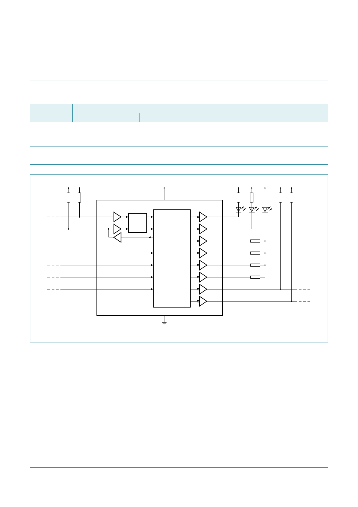
5. Block diagram
2.7 V to 5.5 V
V
R2R1
SCL
SDA
RESET 3
A0 1
PCA9621
14
15
FILTER
DD
16
I2C-BUS SLAVE
TRANSCEIVER
4P0
5P1
6P2
7P3
9P4
R4
R3 R5 R6
LED
LED
high
current
LED
R7
R8
R9
A1 2
A2 13
Fig 1. Block diagram of PCA9621
10 P5
11 P6
12 P7
8
V
SS
R10
output
output
002aaf37
PCA9621 All information provided in this document is subject to legal disclaimers. © NXP B.V. 2011. All rights reserved.
Product data sheet Rev. 1 — 9 March 2011 2 of 18
Page 3
NXP Semiconductors
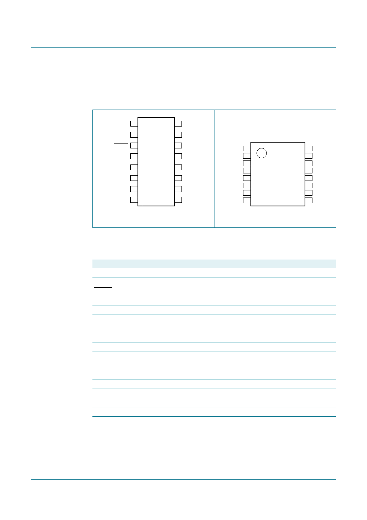
6. Pinning information
6.1 Pinning
PCA9621
65 mA 8-bit 2-wire bus output port
1
A0 V
2
A1 SDA
RESET SCL
3
4
P0 A2
PCA9621D
5
P1 P7
6
P2 P6
7
P3 P5
8
V
SS
Fig 2. Pin configuration for SO16 Fig 3. Pin configuration for TSSOP16
6.2 Pin description
Table 2. Pin description
Symbol Pin Description
A0 1 address input 0
A1 2 address input 1
RESET
P0 4 output port 0
P1 5 output port 1
P2 6 output port 2
P3 7 output port 3
V
SS
P4 9 output port 4
P5 10 output port 5
P6 11 output port 6
P7 12 output port 7
A2 13 address input 2
SCL 14 serial clock line
SDA 15 serial data line
V
DD
3 active LOW reset input
8 negative supply (ground)
16 positive supply
002aaf381
16
DD
15
14
13
12
11
10
9
P4
RESET SCL
1
A0 V
2
A1 SDA
3
4
P0 A2
P1 P7
P2 P6
P3 P5
V
SS
5
6
7
8
PCA9621PW
002aaf382
16
15
14
13
12
11
10
9
DD
P4
PCA9621 All information provided in this document is subject to legal disclaimers. © NXP B.V. 2011. All rights reserved.
Product data sheet Rev. 1 — 9 March 2011 3 of 18
Page 4

NXP Semiconductors
7. Functional description
Refer to Figure 1 “Block diagram of PCA9621”.
7.1 VDD, VSS — DC supply pins
The power supply voltage for the PCA9621 may be any voltage in the range 2.7 V to
5.5 V. All other I/Os are clamped to V
7.2 SCL, SDA — 2-wire bus interface
PCA9621
65 mA 8-bit 2-wire bus output port
and VSS through ESD protection diodes.
DD
The state of the output ports is determined by the Control register, which is set and read
via a 2-wire bus interface using I
(Fm+) I
2
C-bus compatible, though the ports contain ESD protection diodes to the posi tive
and negative supplies. Consequently, V
within the V
and VSS supply levels.
DD
2
C-bus style signalling. The interface is Fast-mode Plus
(voltage at SCL and SDA) must remain
I2C-bus
7.3 P0 to P7 — output ports
There are eight open-drain output ports whose state is de termined by the Con trol register.
Programming a ‘1’ or HIGH to the relevant register bit will turn on the corresponding port,
resulting at a LOW or ‘0’ at the port. In the case of LED driving, this would result in the
LED turning ON.
Programming a ‘0’ or LOW in the register turns off the open-drain port, placing it in a
high-impedance mode.
The ports are protected by ESD diodes to the supplies so they must not be driven above
the V
or below the VSS levels.
DD
7.4 RESET — reset IC to default state
The active LOW RESET input is used to disable the buffer and reset it to its default state.
The RESET
ports, and resetting the state of the I
signal will clear the contents of the Control register, turning off all output
2
C-bus slave transceiver block.
7.5 Power-On Reset (POR)
During power-on, the PCA9621 is internally held in the reset condition for a maximum of
t
= 500 ns. The default condition after reset is for the Control register to be erased
rst
(all zeros), resulting in all output ports being off (high-impedance).
PCA9621 All information provided in this document is subject to legal disclaimers. © NXP B.V. 2011. All rights reserved.
Product data sheet Rev. 1 — 9 March 2011 4 of 18
Page 5
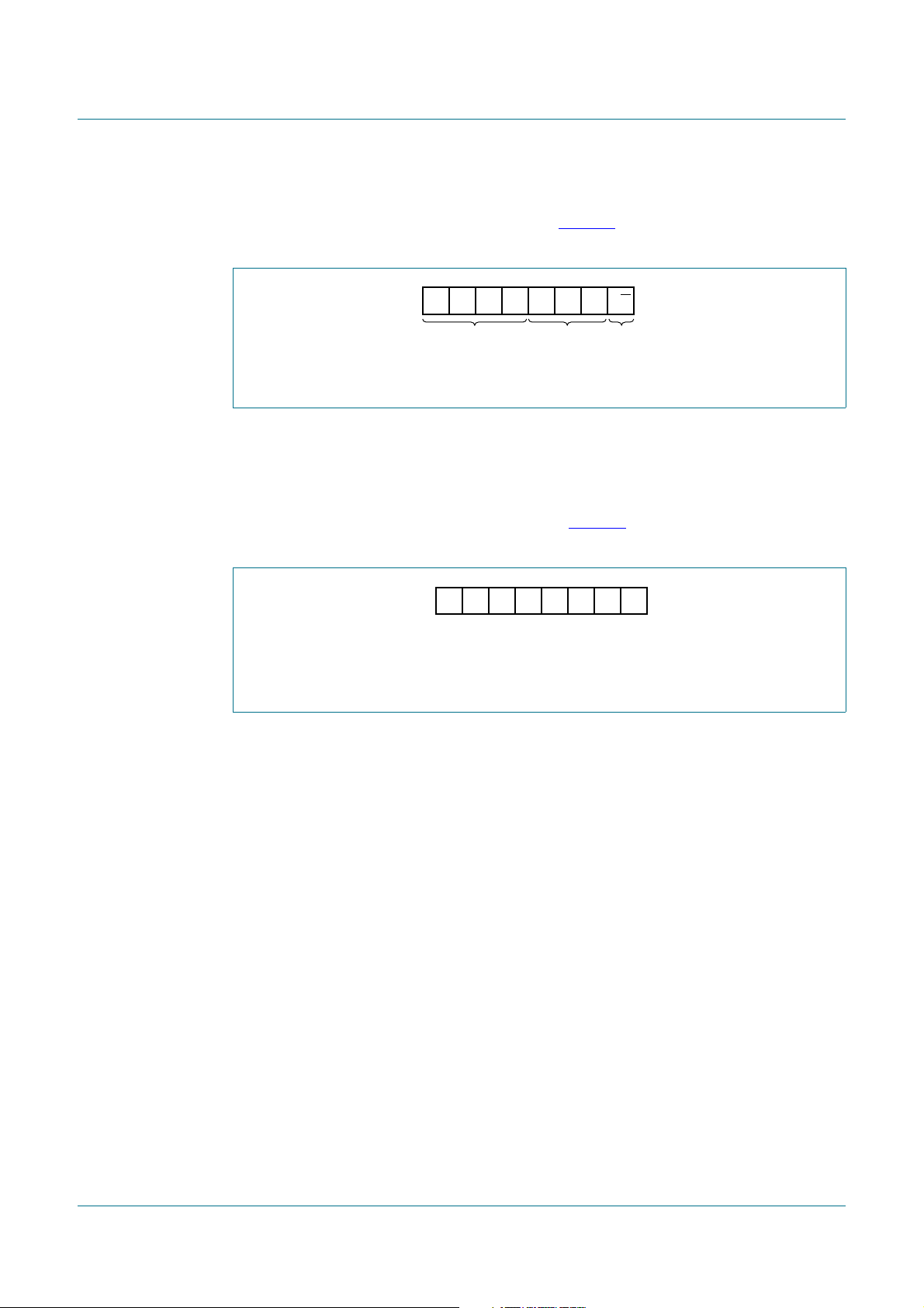
NXP Semiconductors
3
84
7.6 A0, A1, A2 — address lines
The slave address of the PCA9621 is shown in Figure 4. The address pins (A2, A1, A0)
must be driven to a HIGH or LOW level—they are not internally pulled to a default state.
PCA9621
65 mA 8-bit 2-wire bus output port
1 1 0 0 A2 A1 A0 R/W
fixed externally
selectable
read = 1
write = 0
002aaf38
Fig 4. Slave address
The read/write bit must be set LOW to enable a write to the Control register, or HIGH to
read from the Control register.
7.7 Control register
The Control register of the PCA9621 is shown in Figure 5. Each of the four output ports
can be activated independently by setting the appropriate bit in the Control register.
P7 P6 P5 P4 P3 P2 P1 P0MSB LSB
002aaf3
1 = ON (sinking)
0 = OFF (high-impedance)
Fig 5. Control register
A LOW or ‘zero’ bit indicates that the respective channel (P7 to P0) is disabled
(high-impedance). The default reset condition of the register is all zeros, all ports
high-impedance. A HIGH or ‘one’ bit indicates the respective channel is active (sinking).
Example: Programming C1h (1100 0001b) into the Control register results in port s P0, P6
and P7 being ON (sinking) and the remaining ports being OFF (high-impedance).
PCA9621 All information provided in this document is subject to legal disclaimers. © NXP B.V. 2011. All rights reserved.
Product data sheet Rev. 1 — 9 March 2011 5 of 18
Page 6
NXP Semiconductors
5
6
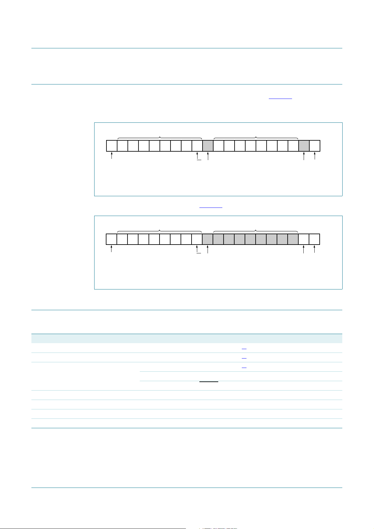
8. Bus transaction
A typical I2C-bus write transaction to the PCA9621 is shown in Figure 6. During a write
transaction, the output ports (P0 to P7) of the PCA9621 are updated upon receipt of the
STOP condition.
PCA9621
65 mA 8-bit 2-wire bus output port
Fig 6. PCA9621 write transaction to Control register
A typical read transaction is shown in Figure 7.
Fig 7. PCA9621 read transaction from Control register
9. Limiting values
slave address
S 1 1 0 0 A2 A1 A0
START
condition
slave address
S 1 1 0 0 A2 A1 A0
START
condition
Control register
0 A P7 P6 P5 P4 P3 P2 P1 P0 A P
R/W acknowledge
from slave
Control register
1 A P7 P6 P5 P4 P3 P2 P1 P0 NA P
R/W acknowledge
from slave
acknowledge
from slave
not acknowledge
from master
STOP
condition
002aaf38
STOP
condition
002aaf38
Table 3. Limiting values
In accordance with the Absolute Maximum Rating System (IEC 60134).
Symbol Parameter Conditions Min Max Unit
V
DD
V
n
I
I
supply voltage
voltage on any other pin
input current output ports (P0 to P7)
[1]
−0.3 +7 V
[1]
VSS− 0.5 VDD+0.5 V
[2]
-100mA
SDA, SCL pins - 40 mA
address pins A0 to A2; RESET
I
SS
P
tot
T
stg
T
amb
[1] Voltages are specified with respect to pin 8 (VSS).
[2] 100 mA for one pin only in the group P0 to P3, and one pin only in the group P4 to P7. Otherwise 70 mA maximum, any pin.
PCA9621 All information provided in this document is subject to legal disclaimers. © NXP B.V. 2011. All rights reserved.
Product data sheet Rev. 1 — 9 March 2011 6 of 18
ground supply current - 550 mA
total power dissipation - 300 mW
storage temperature −55 +125 °C
ambient temperature operating −40 +85 °C
pin - 20 mA
Page 7

NXP Semiconductors
10. Characteristics
PCA9621
65 mA 8-bit 2-wire bus output port
Table 4. Characteristics
T
=−40°C to +85°C; voltages are specified with respect to ground (VSS); VDD= 5.5 V unless otherwise specified.
amb
Symbol Parameter Conditions Min Typ Max Unit
Power supply
V
DD
I
DD
2
I
C-bus ports (SCL, SDA)
V
I2C-bus
V
IL
V
IH
I
LI
V
OL
supply voltage operating 2.7 - 5.5 V
supply current quiescent; VI(RESET pin) = 0 V;
=5.5V
V
DD
--1μA
I2C-bus voltage SDA, SCL VSS− 0.3 - VDD+0.3 V
LOW-level input voltage VDD=2.7V
=5.5V
V
DD
HIGH-level input voltage VDD=2.7V
=5.5V
V
DD
input leakage current pin at VDD or V
SS
[1]
--0.4V
[1]
--0.5V
[1]
1.2 - - V
[1]
2.0 - - V
−1-+1μA
LOW-level output voltage IOL=30mA; VDD= 2.7 V - 260 450 mV
=30mA; VDD= 5.5 V - 140 275 mV
I
OL
Open-drain output ports (P0 to P7)
I
O(sink)
V
OL
output sink current LOW-level; port enabled 65 - - mA
LOW-level output voltage IOL= 65 mA - 440 725 mV
=100μA-1-mV
I
OL
RESET
V
IH
V
IL
V
hys
I
LI
t
w(rst)L
t
rst
t
POR
HIGH-level input voltage VDD= 2.7 V 2.0 - - V
= 5.5 V 4.8 - - V
V
DD
LOW-level input voltage VDD= 2.7 V - - 650 mV
= 5.5 V - - 900 mV
V
DD
hysteresis voltage VDD= 2.7 V 100 - - mV
= 5.5 V 200 - - mV
V
DD
input leakage current pin at VDD or V
LOW-level reset time VI<V
IL
SS
reset time RESET pin; from VI > V
power-on reset pulse time RESET pin; from VI > V
IH
IH
−1-+1μA
[2]
-25-ns
- 250 500 ns
- 250 500 ns
Address pins (A0, A1, A2)
V
IH
V
IL
I
LI
HIGH-level input voltage VDD= 2.7 V 1.7 - - V
= 5.5 V 3.5 - - V
V
DD
LOW-level input voltage VDD= 2.7 V - - 0.7 V
= 5.5 V - - 1.5 V
V
DD
input leakage current pin at VDD or V
SS
−1-+1μA
Timing characteri stics
t
f
t
v(Q)
fall time of both SDA and
SCL signals
data output valid time
RPU = 200 Ω; measured from
70 % VDDto 30 % V
DD
-16-ns
[3]
- - 500 ns
PCA9621 All information provided in this document is subject to legal disclaimers. © NXP B.V. 2011. All rights reserved.
Product data sheet Rev. 1 — 9 March 2011 7 of 18
Page 8

NXP Semiconductors
002aaf372
[1] Supply voltage dependent; refer to graphs (Figure 8 through Figure 10) for typical trend.
[2] Guaranteed by design, not subject to test.
[3] Time between STOP condition and output port (P0 to P7) being asserted.
PCA9621
65 mA 8-bit 2-wire bus output port
250
V
OL
(mV)
200
150
100
50
0
0 1000800400 600200
T
amb
VDD = 5.5 V
2.7 V
(Ω)
R
PU
=25°CI
Fig 8. Typical SDA LOW-level output voltage versus
pull-up resistance
250
V
OL
(mV)
200
150
100
400
V
OL
(mV)
300
200
100
0
−50 150100050
OL
VDD = 2.7 V
5.5 V
=30mA
002aaf373
T
amb
(C)
Fig 9. Typical SDA LOW-level output voltage versus
ambient temperature
002aaf389
50
0
T
=25°C; VDD=5.5V
amb
0806020 40
I
O(sink)
(mA)
Fig 10. Typical output port (P0 to P7) LOW-level output voltage versus LOW-level output sink current
PCA9621 All information provided in this document is subject to legal disclaimers. © NXP B.V. 2011. All rights reserved.
Product data sheet Rev. 1 — 9 March 2011 8 of 18
Page 9

NXP Semiconductors
7
11. Application information
Figure 11 shows the PCA9621 in conjunction with the PCA9646 bus multiplexer in a LED
drive application. Each PCA9621 can drive 8 LEDs, and using the address pins on the IC,
up to 8 uniquely addressed devices can sit on one bus branch. The PCA9646 has four
such outputs, giving 256 LEDs in the structure shown.
By additionally using the address pins on the PCA9646, the entire structure may be
repeated 8 times, allowing 2048 LEDs to be uniquely driven. By additionally placing
PCA9646’s in series (refer to the PCA9646 data sheet), the structure may be further
extensively multiplied into a huge array.
5 V
PCA9621
65 mA 8-bit 2-wire bus output port
V
DD
SCL
SDA
BUS MASTER
U2
SC2
SD2
buses SC2/SD2, SC3/SD3
as shown for
SC0/SD0, SC1/SD1
SC3
SD3
Entire structure can be repeated
8 times using PCA9646 address pins
(further expansion possible).
R1
R3 R4
R5 R6
Fig 11. PCA9621 in a large LED array
8 LEDs
8 LEDs
R8
SCL
P[7:0]
PCA9621
U10
R10
SCL
P[7:0]
PCA9621
U18
SC0
SD0
DD
V
SDA
SDA
8 LEDs
8
SC1
SD1
DD
V
8 LEDs
8
002aaf39
R2
SCL
SDA
RESET
V
DD
SC0
SD0
PCA9646
R7
DD
V
SCL
SDA
8
P[7:0]
PCA9621
SC2
SD2
SC3
SD3
A0
A1
A2
V
U1
SS
U3
R9
SC1
SD1
SCL
PCA9621
U11
8 × PCA9621
each with
8 LEDs = 64 LEDs
DD
V
SDA
8
P[7:0]
8 × PCA9621
each with
8 LEDs = 64 LEDs
PCA9621 All information provided in this document is subject to legal disclaimers. © NXP B.V. 2011. All rights reserved.
Product data sheet Rev. 1 — 9 March 2011 9 of 18
Page 10

NXP Semiconductors
8
9
Figure 12 shows a simple 7-segment display drive arrangement. All of the 7 segments
plus decimal point can be driven from a single PCA9621 . By using the address pi ns, up to
8 digits can be addressed from a single bus. When running at 1 MHz, all 8 digits can be
updated in less than 0.2 ms.
PCA9621
65 mA 8-bit 2-wire bus output port
Further, by using the arrangement described above and shown in Figure 11
, the number
of digits driven may be increased significantly.
5 V
P0
P1
P2
P3
P4
P5
P6
P7
R1 R2
repeat up to 8 times using
address pins on PCA9621
002aaf39
SCL
SDA
V
DD
SCL
SDA
3
A[2:0]
RESET
PCA9621
U1
Fig 12. PCA9621 as 7-segment display driver
Figure 13 shows the PCA9621 used in conjunction with other NXP Semiconductors
2-wire bus buffers to form a multiplexer arrangement. Using the PCA9621 to control
multiples of either PCA9521 or PCA9522 produces an isolating bus switch/multiplexer
that has fully compliant I
2
C-bus I/O levels, low offset voltages, and large noise margins.
Using PCA9522 in this arrangement additionally provides ‘hot-swap’ capability.
3.3 V
SCL
SDA
R1 R2
V
DD
SCL
SDA
3
A[2:0]
RESET
P0
P1
P2
P3
P4
P5
P6
P7
PCA9621
U1
SA1
SB1
PCA9521
EN
U2
3.3 V
SCLC
SDAC
PCA9522
EN
U3
V
CC
SA2
SB2
(1)
V
CC
SCLB
SDAB
(1)
RDY
400 pF
multiple
isolated
buses
400 pF
002aaf39
(1)
(1)
Address lines allow this structure to be repeated 8 more times.
(1) Or PCA9525 (400 pF), or PCA9605 (4000 pF), or PCA9646 (4 × 4000 pF).
Fig 13. PCA9621 as part of a fully isolating I2C-bus multiplexer
PCA9621 All information provided in this document is subject to legal disclaimers. © NXP B.V. 2011. All rights reserved.
Product data sheet Rev. 1 — 9 March 2011 10 of 18
Page 11

NXP Semiconductors
S
-1
12. Package outline
PCA9621
65 mA 8-bit 2-wire bus output port
O16: plastic small outline package; 16 leads; body width 3.9 mm
y
Z
16
pin 1 index
1
D
c
9
A
2
A
1
8
e
w M
b
p
E
H
E
detail X
A
Q
(A )
3
θ
L
p
L
SOT109
X
v M
A
A
0 2.5 5 mm
scale
DIMENSIONS (inch dimensions are derived from the original mm dimensions)
mm
OUTLINE
VERSION
SOT109-1
A
A1A2A3b
max.
0.25
1.75
0.10
0.010
0.069
0.004
p
1.45
1.25
0.057
0.049
IEC JEDEC JEITA
076E07 MS-012
0.25
0.01
0.49
0.36
0.019
0.014
0.25
0.19
0.0100
0.0075
UNIT
inches
Note
1. Plastic or metal protrusions of 0.15 mm (0.006 inch) maximum per side are not included.
(1)E(1) (1)
cD
10.0
9.8
0.39
0.38
REFERENCES
eHELLpQZywv θ
4.0
3.8
0.16
0.15
1.27
0.05
6.2
5.8
0.244
0.228
1.05
0.041
1.0
0.4
0.039
0.016
0.7
0.25
0.6
0.028
0.01 0.004
0.020
EUROPEAN
PROJECTION
0.25 0.1
0.01
0.7
0.3
0.028
0.012
ISSUE DATE
99-12-27
03-02-19
o
8
o
0
Fig 14. Package outline SOT109-1 (SO16)
PCA9621 All information provided in this document is subject to legal disclaimers. © NXP B.V. 2011. All rights reserved.
Product data sheet Rev. 1 — 9 March 2011 11 of 18
Page 12

NXP Semiconductors
-1
PCA9621
65 mA 8-bit 2-wire bus output port
TSSOP16: plastic thin shrink small outline package; 16 leads; body width 4.4 mm
D
c
y
Z
16
pin 1 index
9
A
2
18
w M
b
e
p
A
1
E
H
E
L
detail X
SOT403
A
X
v M
A
Q
(A )
3
A
θ
L
p
0 2.5 5 mm
scale
DIMENSIONS (mm are the original dimensions)
UNIT A1A2A3b
Notes
1. Plastic or metal protrusions of 0.15 mm maximum per side are not included.
2. Plastic interlead protrusions of 0.25 mm maximum per side are not included.
A
max.
0.15
mm
1.1
OUTLINE
VERSION
SOT403-1 MO-153
0.05
0.95
0.80
IEC JEDEC JEITA
0.25
p
0.30
0.19
(1)E(2) (1)
cD
0.2
5.1
0.1
4.9
REFERENCES
eHELLpQZywv θ
4.5
4.3
0.65
6.6
6.2
0.75
0.50
0.4
0.3
EUROPEAN
PROJECTION
0.13 0.10.21
0.40
0.06
ISSUE DATE
99-12-27
03-02-18
o
8
o
0
Fig 15. Package outline SOT403-1 (TSSOP16)
PCA9621 All information provided in this document is subject to legal disclaimers. © NXP B.V. 2011. All rights reserved.
Product data sheet Rev. 1 — 9 March 2011 12 of 18
Page 13

NXP Semiconductors
13. Handling information
CAUTION
This device is sensitive to ElectroStatic Discharge (ESD). Observe precautions for handling
electrostatic sensitive devices.
Such precautions are described in the ANSI/ESD S20.20, IEC/ST 61340-5, JESD625-A or
equivalent standards.
14. Soldering of SMD packages
This text provides a very brief insight into a complex technology . A more in-depth account
of soldering ICs can be found in Application Note AN10365 “Surface mount reflow
soldering description”.
14.1 Introduction to soldering
Soldering is one of the most common methods through which packages are attached to
Printed Circuit Boards (PCBs), to form electrical circuits. The soldered joint provides both
the mechanical and the electrical connection. There is no single soldering method that is
ideal for all IC packages. Wave soldering is often preferred when through-hole and
Surface Mount Devices (SMDs) are mixed on one printed wiring board; however, it is not
suitable for fine pitch SMDs. Reflow soldering is ideal for the small pitches and high
densities that come with increased miniaturization.
PCA9621
65 mA 8-bit 2-wire bus output port
14.2 Wave and reflow soldering
Wave soldering is a joining technology in which the joints are made by so lder coming from
a standing wave of liquid solder. The wave soldering process is suitable for the following:
• Through-hole components
• Leaded or leadless SMDs, which are glued to the surface of the printed circuit board
Not all SMDs can be wave soldered. Packages with solder balls, and some leadless
packages which have solder lands underneath the body, cannot be wave soldered. Also,
leaded SMDs with leads having a pitch smaller than ~0.6 mm cannot be wave soldered,
due to an increased probability of bridging.
The reflow soldering process involves applying solder paste to a board, followed by
component placement and exposure to a temperature profile. Leaded packages,
packages with solder balls, and leadless packages are all reflow solderable.
Key characteristics in both wave and reflow soldering are:
• Board specifications, including the board finish, solder masks and vias
• Package footprints, including solder thieves and orientation
• The moisture sensitivity level of the packages
• Package placement
• Inspection and repair
• Lead-free soldering versus SnPb soldering
PCA9621 All information provided in this document is subject to legal disclaimers. © NXP B.V. 2011. All rights reserved.
Product data sheet Rev. 1 — 9 March 2011 13 of 18
Page 14

NXP Semiconductors
14.3 Wave soldering
Key characteristics in wave soldering are:
• Process issues, such as application of adhesive and flux, clinching of leads, board
• Solder bath specifications, including temperature and impurities
14.4 Reflow soldering
Key characteristics in reflow soldering are:
• Lead-free versus SnPb soldering; note that a lead-free reflow process usually lea ds to
• Solder paste printing issues including smearing, release, and adjusting the process
• Reflow temperature profile; this profile includes preheat, reflow (in which the board is
Table 5. SnPb eutect ic process (from J-STD-020C)
Package thickness (mm) Packag e reflow temperature (°C)
< 2.5 235 220
≥ 2.5 220 220
PCA9621
65 mA 8-bit 2-wire bus output port
transport, the solder wave parameters, and the time during which components are
exposed to the wave
higher minimum peak temperatures (see Figure 16
reducing the process window
window for a mix of large and small components on one board
heated to the peak temperature) and cooling down. It is imperative that the peak
temperature is high enough for the solder to make reliable solder joint s (a solder paste
characteristic). In addition, the peak temperature must be low enough that the
packages and/or boards are not damaged. The peak temperature of the package
depends on package thickness and volume and is classified in accordance with
Table 5
and 6
Volume (mm3)
< 350 ≥ 350
) than a SnPb process, thus
Table 6. Le ad-free process (from J-STD-020C)
Package thickness (mm) Packag e reflow temperature (°C)
Volume (mm3)
< 350 350 to 2000 > 2000
< 1.6 260 260 260
1.6 to 2.5 260 250 245
> 2.5 250 245 245
Moisture sensitivity precautions, as indicated on the packing, must be respected at all
times.
Studies have shown that small packages reach higher temperatures during reflow
soldering, see Figure 16
PCA9621 All information provided in this document is subject to legal disclaimers. © NXP B.V. 2011. All rights reserved.
Product data sheet Rev. 1 — 9 March 2011 14 of 18
.
Page 15

NXP Semiconductors
4
Fig 16. Temperature profiles for large and small components
maximum peak temperature
temperature
MSL: Moisture Sensitivity Level
= MSL limit, damage level
minimum peak temperature
= minimum soldering temperature
PCA9621
65 mA 8-bit 2-wire bus output port
peak
temperature
time
001aac84
For further information on temperature profiles, refer to Application Note AN10365
“Surface mount reflow soldering description”.
15. Abbreviations
Table 7. Abbreviations
Acronym Description
CMOS Complementary Metal-Oxide Semiconductor
ESD ElectroStatic Discharge
2
C-bus Inter-Integrated Circuit bus
I
I/O Input/Output
IC Integrated Circuit
LED Light-Emitting Diode
PMBus Power Management Bus
POR Power-On Reset
SMBus System Management Bus
16. References
[1] UM10204, “I2C-bus specification and user manual” — NXP Semiconductors;
www.nxp.com/documents/user_manual/UM10204.pdf
17. Revision history
Table 8. Revision history
Document ID Release date Data sheet status Change notice Supersedes
PCA9621 v.1 20110309 Product data sheet - -
PCA9621 All information provided in this document is subject to legal disclaimers. © NXP B.V. 2011. All rights reserved.
Product data sheet Rev. 1 — 9 March 2011 15 of 18
Page 16

NXP Semiconductors
PCA9621
65 mA 8-bit 2-wire bus output port
18. Legal information
18.1 Data sheet status
Document status
Objective [short] data sheet Development This document contains data from the objective specification for product development.
Preliminary [short] data sheet Qualification This document contains data from the preliminary specification.
Product [short] data sheet Production This document contains the product specification.
[1] Please consult the most recently issued document before initiating or completing a design.
[2] The term ‘short data sheet’ is explained in section “Definitions”.
[3] The product status of device(s) described in this document may have changed since thi s document w as published and may dif fe r in case of multiple devices. The latest product status
information is available on the Internet at URL http://www.nxp.com.
[1][2]
Product status
[3]
Definition
18.2 Definitions
Draft — The document is a draft version only. The content is still under
internal review and subject to formal approval, which may result in
modifications or additions. NXP Semiconductors does not give any
representations or warranties as to the accuracy or completeness of
information included herein and shall have no liability for the consequences of
use of such information.
Short data sheet — A short data sheet is an extract from a full data sheet
with the same product type number(s) and title. A short data sheet is intended
for quick reference only and should not be relied u pon to co nt ain det ailed and
full information. For detailed and full information see the relevant full data
sheet, which is available on request via the local NXP Semiconductors sales
office. In case of any inconsistency or conflict with the short data sheet, the
full data sheet shall prevail.
Product specification — The information and data provided in a Product
data sheet shall define the specification of the product as agreed between
NXP Semiconductors and its customer, unless NXP Semiconductors and
customer have explicitly agreed otherwise in writing. In no event however,
shall an agreement be valid in which the NXP Semiconductors product is
deemed to offer functions and qualities beyond those described in the
Product data sheet.
18.3 Disclaimers
Limited warranty and liability — Information in this document is believed to
be accurate and reliable. However, NXP Semiconductors does not give any
representations or warranties, expressed or implied, as to the accuracy or
completeness of such information and shall have no liability for the
consequences of use of such information.
In no event shall NXP Semiconductors be lia ble for any indirect, incidental,
punitive, special or consequential damages (including - without limitation - lost
profits, lost savings, business interruption, costs related to the removal or
replacement of any products or rework charges) whether or not such
damages are based on tort (including negligence), warranty, breach of
contract or any other legal theory.
Notwithstanding any damages that customer might incur for any reason
whatsoever, NXP Semi conductors’ aggregat e and cumulative liabil ity towards
customer for the products described herein shall be limited in accordance
with the Terms and conditions of commercial sale of NXP Semiconductors.
Right to make changes — NXP Semiconductors reserves the right to make
changes to information published in this document, including without
limitation specifications and product descriptions, at any time and without
notice. This document supersedes and replaces all information supplied prior
to the publication hereof.
Suitability for use — NXP Semiconductors products are not designed,
authorized or warranted to be suitable for use in life support, life-critical or
safety-critical systems or equipment, nor in applications where failure or
malfunction of an NXP Semiconductors product can reasonabl y be expected
to result in personal injury, death or severe property or environmental
damage. NXP Semiconductors accepts no liability for inclusion and/or use of
NXP Semiconductors products in such equipment or applications and
therefore such inclusion and/or use is at the customer’s own risk.
Applications — Applications that are described herein for any of these
products are for illustrative purposes only. NXP Semiconductors makes no
representation or warranty that such applications will be suitable for the
specified use without further testing or modification.
Customers are responsible for the design and operation of their applications
and products using NXP Semiconductors products, and NXP Semiconductors
accepts no liability for any assistance with applications or customer product
design. It is customer’s sole responsibility to determine whether the NXP
Semiconductors product is suitable and fit for the customer’s applications and
products planned, as well as for the planned application and use of
customer’s third party customer(s). Customers should provide appropriate
design and operating safeguards to minimize the risks associated with their
applications and products.
NXP Semiconductors does not accept any liability related to any default ,
damage, costs or problem which is based on any weakness or default in the
customer’s applications or products, or the application or use by customer’s
third party customer(s). Customer is responsible for doing all necessary
testing for the customer’s applications and products using NXP
Semiconductors products in order to avoid a default of the applications and
the products or of the application or use by customer’s third part y
customer(s). NXP does not accept any liability in this respect.
Limiting values — Stress above one or more limiting values (as defined in
the Absolute Maximum Ratings System of IEC 60134) will cause permanent
damage to the device. Limiting values are stress ratings only and (proper)
operation of the device at these or any other conditions above those given in
the Recommended operating conditions section (if present) or the
Characteristics sections of this document is not warranted. Constant or
repeated exposure to limiting values will permanently and irreversibly affect
the quality and reliability of the device.
Terms and conditions of commercial sale — NXP Semiconductors
products are sold subject to the general terms and conditions of commercial
sale, as published at http://www.nxp.com/profile/terms
agreed in a valid written individual agreement. In case an individual
agreement is concluded only the terms and conditions of the respective
agreement shall apply. NXP Semiconductors hereby expressly objects to
applying the customer’s general terms and conditions with regard to the
purchase of NXP Semiconductors products by customer.
No offer to sell or license — Nothing in this document may be interpreted or
construed as an offer to sell product s that is ope n for accept ance or the gr ant,
conveyance or implication of any license under any copyrights, patents or
other industrial or intellectual property rights.
Export control — This document as well as the item(s) described herein
may be subject to export control regulations. Export might require a prior
authorization from national authorities.
, unless otherwise
PCA9621 All information provided in this document is subject to legal disclaimers. © NXP B.V. 2011. All rights reserved.
Product data sheet Rev. 1 — 9 March 2011 16 of 18
Page 17

NXP Semiconductors
PCA9621
65 mA 8-bit 2-wire bus output port
Non-automotive qualified products — Unless this data sheet expressly
states that this specific NXP Semiconductors product is automotive qualified,
the product is not suitable for automotive use. It i s neither qua lif ied nor test ed
in accordance with automotive testing or application requirements. NXP
Semiconductors accepts no liability for inclusion and/or use of
non-automotive qualified products in automotive equ ipment or applications.
In the event that customer uses the product for design-in and use in
automotive applications to automotive specifications and standards, customer
(a) shall use the product without NXP Semiconductors’ warranty of the
product for such automotive applications, use and specifications, and (b)
whenever customer uses the product for automotive applications beyond
NXP Semiconductors’ specifications such use shall be solely at customer’s
own risk, and (c) customer fully indemnifies NXP Semiconductors for any
liability, da mages or failed produ ct cl aims resulting from custome r design and
use of the product for automotive applications beyond NXP Semiconductors’
standard warranty and NXP Semiconductors’ product specifications.
18.4 Trademarks
Notice: All referenced brands, prod uct names, service names and trad emarks
are the property of their respective owners.
2
I
C-bus — logo is a trademark of NXP B.V.
19. Contact information
For more information, please visit: http://www.nxp.com
For sales office addresses, please send an email to: salesaddresses@nxp.com
PCA9621 All information provided in this document is subject to legal disclaimers. © NXP B.V. 2011. All rights reserved.
Product data sheet Rev. 1 — 9 March 2011 17 of 18
Page 18

NXP Semiconductors
20. Contents
1 General description. . . . . . . . . . . . . . . . . . . . . . 1
2 Features and benefits . . . . . . . . . . . . . . . . . . . . 1
3 Applications. . . . . . . . . . . . . . . . . . . . . . . . . . . . 1
4 Ordering information. . . . . . . . . . . . . . . . . . . . . 2
5 Block diagram . . . . . . . . . . . . . . . . . . . . . . . . . . 2
6 Pinning information. . . . . . . . . . . . . . . . . . . . . . 3
6.1 Pinning . . . . . . . . . . . . . . . . . . . . . . . . . . . . . . . 3
6.2 Pin description . . . . . . . . . . . . . . . . . . . . . . . . . 3
7 Functional description . . . . . . . . . . . . . . . . . . . 4
7.1 V
7.2 SCL, SDA — 2-wire bus interface . . . . . . . . . . 4
7.3 P0 to P7 — output ports . . . . . . . . . . . . . . . . . . 4
7.4 RESET
7.5 Power-On Reset (POR) . . . . . . . . . . . . . . . . . . 4
7.6 A0, A1, A2 — address lines . . . . . . . . . . . . . . . 5
7.7 Control register. . . . . . . . . . . . . . . . . . . . . . . . . 5
8 Bus transaction . . . . . . . . . . . . . . . . . . . . . . . . . 6
9 Limiting values. . . . . . . . . . . . . . . . . . . . . . . . . . 6
10 Characteristics. . . . . . . . . . . . . . . . . . . . . . . . . . 7
11 Application information. . . . . . . . . . . . . . . . . . . 9
12 Package outline . . . . . . . . . . . . . . . . . . . . . . . . 11
13 Handling information. . . . . . . . . . . . . . . . . . . . 13
14 Soldering of SMD packages . . . . . . . . . . . . . . 13
14.1 Introduction to soldering. . . . . . . . . . . . . . . . . 13
14.2 Wave and reflow soldering . . . . . . . . . . . . . . . 13
14.3 Wave soldering. . . . . . . . . . . . . . . . . . . . . . . . 14
14.4 Reflow soldering. . . . . . . . . . . . . . . . . . . . . . . 14
15 Abbreviations. . . . . . . . . . . . . . . . . . . . . . . . . . 15
16 References . . . . . . . . . . . . . . . . . . . . . . . . . . . . 15
17 Revision history. . . . . . . . . . . . . . . . . . . . . . . . 15
18 Legal information. . . . . . . . . . . . . . . . . . . . . . . 16
18.1 Data sheet status . . . . . . . . . . . . . . . . . . . . . . 16
18.2 Definitions. . . . . . . . . . . . . . . . . . . . . . . . . . . . 16
18.3 Disclaimers. . . . . . . . . . . . . . . . . . . . . . . . . . . 16
18.4 Trademarks. . . . . . . . . . . . . . . . . . . . . . . . . . . 17
19 Contact information. . . . . . . . . . . . . . . . . . . . . 17
20 Contents . . . . . . . . . . . . . . . . . . . . . . . . . . . . . . 18
, VSS — DC supply pins . . . . . . . . . . . . . . . 4
DD
— reset IC to default state. . . . . . . . . . 4
PCA9621
65 mA 8-bit 2-wire bus output port
Please be aware that important notices concerning this document and the product(s)
described herein, have been included in section ‘Legal information’.
© NXP B.V. 2011. All rights reserved.
For more information, please visit: http://www.nxp.com
For sales office addresses, please send an email to: salesaddresses@nxp.com
Date of release: 9 March 2011
Document identifier: PCA9621
 Loading...