

DATA SH EET
ook, halfpage
DISCRETE SEMICONDUCTORS
M3D109
PBSS5350X
50 V, 3 A
PNP low V
Product data sheet
Supersedes data of 2003 Nov 21
CEsat
(BISS) transistor
2004 Nov 04
NXP Semiconductors Product data sheet
9
1
2
3
50 V, 3 A
PNP low V
CEsat
FEATURES
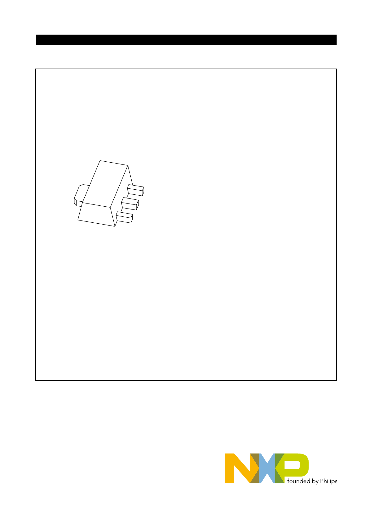
• SOT89 (SC-62) package
• Low collector-emitter saturation voltage V
• High collector current capability: IC and I
• Higher efficiency leading to less heat generation
• Reduced printed-circuit board requirements.
APPLICATIONS
• Power management
– DC/DC converters
– Supply line switching
– Battery charger
– LCD backlighting.
• Peripheral drivers
– Driver in low supply voltage applications (e.g. lamps
and LEDs).
– Inductive load driver (e.g. relays,
buzzers and motors).
(BISS) transistor
CEsat
CM
PBSS5350X
QUICK REFERENCE DATA
SYMBOL PARAMETER MAX. UNIT
V
CEO
I
C
I
CM
R
CEsat
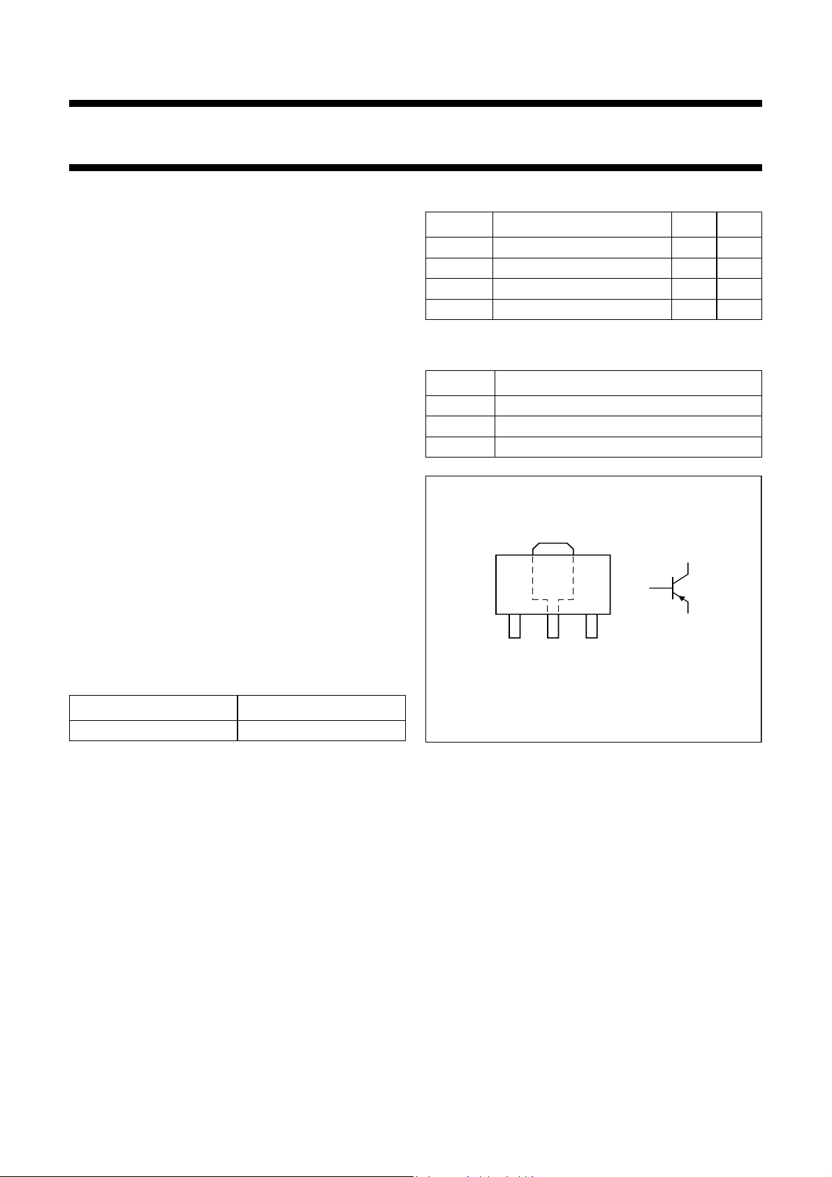
PINNING
PIN DESCRIPTION
collector-emitter voltage −50 V
collector current (DC) −3 A
peak collector current −5 A
equivalent on-resistance 135 mΩ
1 emitter
2 collector
3 base
DESCRIPTION
PNP low V
transistor in a SOT89 plastic package.
CEsat
NPN complement: PBSS4350X.
MARKING
T YPE NUMBER MARKING CODE
PBSS5350X S46
sym07
321
Fig.1 Simplified outline (SOT89) and symbol.
2004 Nov 04 2
NXP Semiconductors Product data sheet
50 V, 3 A
PBSS5350X
PNP low V
ORDERING INFORMATION
T YPE NUMBER
PBSS5350X SC-62 plastic surface mounted package; collector pad for go od hea t
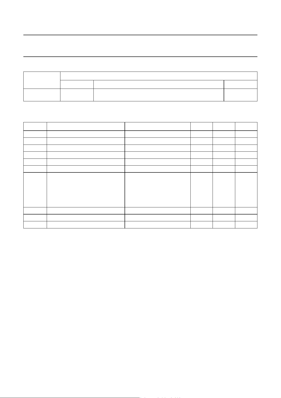
LIMITING VALUES
In accordance with the Absolu te Maximum Rating System (IEC 60134).
SYMBOL PARAMETER CONDITIONS MIN. MAX. UNIT
V
V
V
I
I
I
P
T
T
T
CBO
CEO
EBO
C
CM
B
tot
stg
j
amb
collector-base voltage open emitter − −50 V
collector-emitter voltage open base − −50 V
emitter-base voltage open collector − −5 V
collector current (DC) note 4 − −3 A
peak collector current limited by T
base current (DC) − −0.5 A
total power dissipation T
storage temperature −65 +150 °C
junction temperature − 150 °C
ambient temperature −65 +150 °C
(BISS) transistor
CEsat
PACKAGE
NAME DESCRIPTION VERSION
transfer; 3 leads
− −5 A
amb
j(max)
≤ 25 °C
note 1 − 550 mW
note 2 − 1 W
note 3 − 1.4 W
note 4 − 1.6 W
SOT89
Notes
1. Device mounted on a FR4 printed-circuit board; single-sided copper; tin-plated; standard footprint.
2. Device mounted on a FR4 printed-circuit board; single-sided copper; tin-plated; mounting pad for collector 1 cm2.
3. Device mounted on a FR4 printed-circuit board; single-sided copper; tin-plated; mounting pad for collector 6 cm2.
4. Device mounted on a ceramic printed-circuit board 7 cm2, single-sided copper, tin-plated.
2004 Nov 04 3
NXP Semiconductors Product data sheet
50 V, 3 A
PNP low V
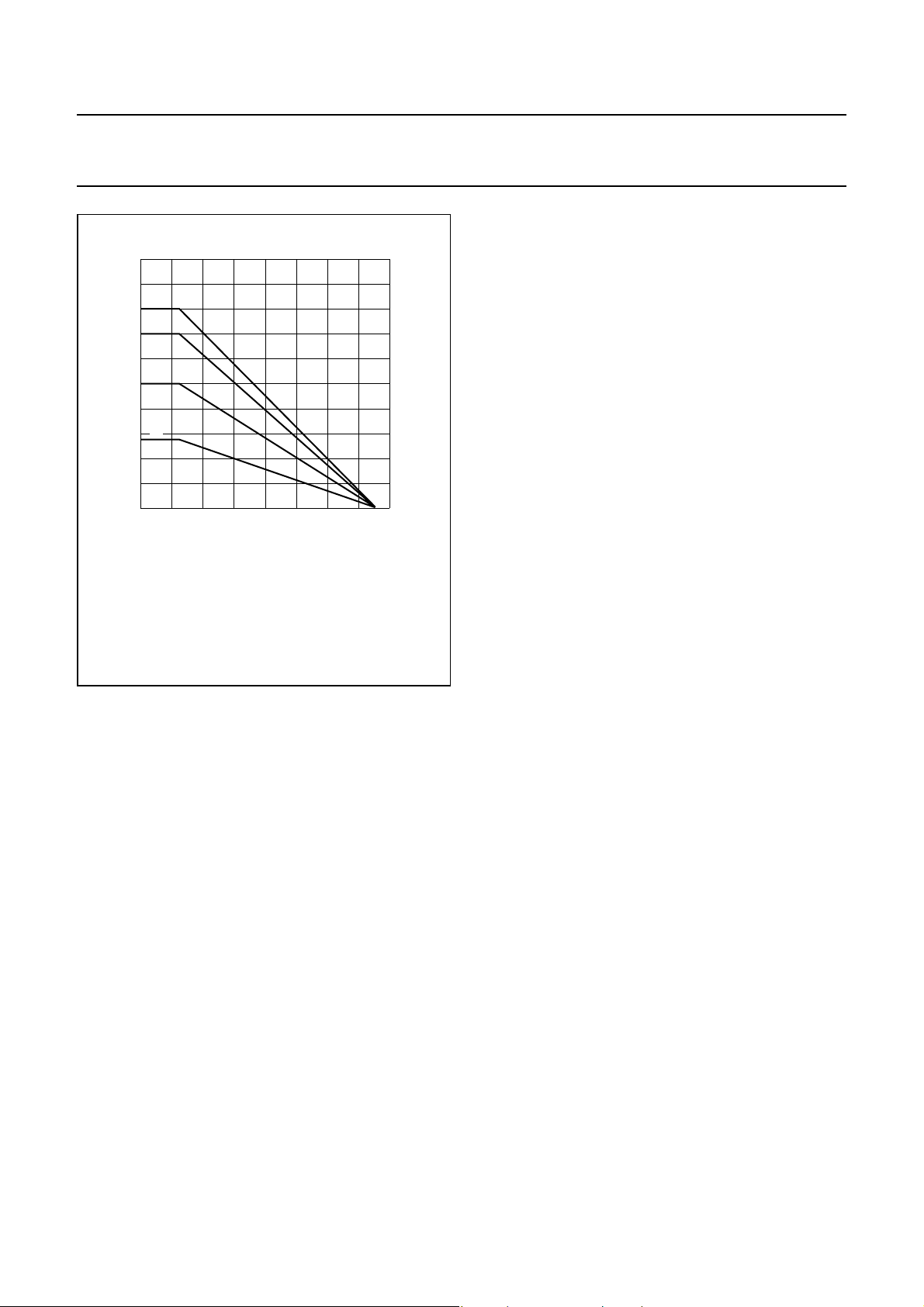
handbook, halfpage
2
P
tot
(W)
(1)
1.6
(2)
1.2
(3)
0.8
(4)
0.4
0
0 40 80 160
(1) Ceramic PCB; 7 cm2
mounting pad for collector.
(2) FR4 PCB; 6 cm2 copper
mounting pad for collector.
(BISS) transistor
CEsat
(3) FR4 PCB; 1 cm
mounting pad for collector.
(4) Standard footprint.
120
T
amb
MLE186
(°C)
2
PBSS5350X
copper
Fig.2 Power derating curves.
2004 Nov 04 4

NXP Semiconductors Product data sheet
50 V, 3 A
PBSS5350X
PNP low V
THERMAL CHARACTERISTICS
SYMBOL PARAMETER CONDITIONS VALUE UNIT
R
th(j-a)
R
th(j-s)
Notes
1. Device mounted on a FR4 printed-circuit board; single-sided copper; tin-plated; standard footprint.
2. Device mounted on a FR4 printed-circuit board; single-sided copper; tin-plated; mounting pad for collector 1 cm2.
3. Device mounted on a FR4 printed-circuit board; single-sided copper; tin-plated; mounting pad for collector 6 cm2.
4. Device mounted on a ceramic printed-circuit board 7 cm2, single-sided copper, tin-plated.
Z
th(j-a)
(K/W)
thermal resistance from junction to ambient in free air
thermal resistance from junction to soldering point 16 K/W
3
10
duty cycle =
1.00
0.75
2
10
0.50
0.33
0.20
0.10
0.05
10
0.02
0.01
(BISS) transistor
CEsat
note 1 225 K/W
note 2 125 K/W
note 3 90 K/W
note 4 80 K/W
006aaa243
1
0
−1
10
−5
10
Mounted on FR4 printed-circu i t board; standard footprint.
−4
10
−3
10
−2
−1
10
1
1010
2
10
tp (s)
3
10
Fig.3 Transient thermal impedance as a function of pulse time; typical values.
2004 Nov 04 5

NXP Semiconductors Product data sheet
006aaa245
50 V, 3 A
PNP low V
3
10
Z
th(j-a)
(K/W)
duty cycle =
1.00
2
10
0.75
0.50
0.33
0.20
0.10
10
0.05
0.02
0.01
1
0
−1
10
−5
10
Mounted on FR4 printed-circuit board; mounting pad for collector 1 cm2.
(BISS) transistor
CEsat
−4
10
−3
10
−2
PBSS5350X
006aaa244
−1
10
1
1010
2
10
tp (s)
3
10
Fig.4 Transient thermal impedance as a function of pulse time; typical values.
3
10
Z
th(j-a)
(K/W)
duty cycle =
2
10
1.00
0.75
0.50
0.33
0.20
10
0.10
0.05
0.02
0.01
1
0
−1
10
−5
10
Mounted on FR4 printed-circuit board; mounting pad for collector 6 cm2.
−4
10
−3
10
−2
Fig.5 Transient thermal impedance as a function of pulse time; typical values.
−1
10
1
1010
2
10
tp (s)
3
10
2004 Nov 04 6

NXP Semiconductors Product data sheet
50 V, 3 A
PBSS5350X
PNP low V
CHARACTERISTICS
T
= 25 °C unless otherwise specified.
amb
SYMBOL PARAMETER CONDITIONS MIN. TYP. MAX. UNIT
I
CBO
I
CES
I
EBO
h
V
R
V
V
f
T
C
FE
CEsat
CEsat
BEsat
BEon
c
collector-base cut-off curren t VCB = −50 V; IE = 0 A − − −100 nA
collector-emitter cut-off current VCE = −50 V; VBE = 0 V − − −100 nA
emitter-base cut-off current VEB = −5 V; IC = 0 A − − −100 nA
DC current gain VCE = −2 V
collector-emitter saturation
voltage
equivalent on-resistance IC = −2 A; IB = −200 mA; note 1 − 90 135 mΩ
base-emitter saturation vo ltage IC = −2 A; IB = −100 mA − − −1.1 V
base-emitter turn-on voltage VCE = −2 V; IC = −1 A −1.1 − − V
transition frequency IC = −100 mA; VCE = −5 V;
collector capacitance VCB = −10 V; IE = ie = 0 A; f = 1 MHz − − 35 pF
(BISS) transistor
CEsat
VCB = −50 V; IE = 0 A; Tj = 150 °C − − −50 μA
IC = −0.1 A 200 − −
IC = −0.5 A 200 − −
IC = −1 A; note 1 200 − 450
IC = −2 A; note 1 130 − −
IC = −3 A; note 1 80 − −
IC = −0.5 A; IB = −50 mA − − −90 mV
IC = −1 A; IB = −50 mA − − −180 mV
IC = −2 A; IB = −100 mA − − −320 mV
IC = −2 A; IB = −200 mA; note 1 − − −270 mV
IC = −3 A; IB = −300 mA; note 1 − − −390 mV
IC = −3 A; IB = −300 mA; note 1 − − −1.2 V
100 − − MHz
f = 100 MHz
Note
1. Pulse test: tp ≤ 300 μs; δ ≤ 0.02.
2004 Nov 04 7

NXP Semiconductors Product data sheet
50 V, 3 A
PNP low V
600
handbook, halfpage
h
FE
400
200
0
−1
−10
VCE = −2 V.
(1) T
= 100 °C.
amb
(2) T
= 25 °C.
amb
(3) T
= −55 °C.
amb
CEsat
−1 −10
(BISS) transistor
MLE171
(1)
(2)
(3)
−10
2
−103−10
IC (mA)
4
−1.2
handbook, halfpage
V
BE
(V)
−0.8
−0.4
0
−1
−10
VCE = −2 V.
(1) T
= −55 °C.
amb
(2) T
= 25 °C.
amb
(3) T
= 100 °C.
amb
−1 −10
PBSS5350X
(1)
(2)
(3)
−10
2
−10
3
IC (mA)
MLE170
−10
4
Fig.6 DC current gain as a function of collector
current; typical values.
−1
handbook, halfpage
V
CEsat
(V)
−1
−10
−2
−10
−3
−10
−1
−10
IC/IB = 20.
(1) T
= 100 °C.
amb
(2) T
= 25 °C.
amb
(3) T
= −55 °C.
amb
(2)
−1 −10
(1)
(3)
2
−10
MLE173
−103−10
IC (mA)
Fig.7 Base-emitter voltage as a function of
collector current; typical values.
−10
MLE174
3
IC (mA)
−10
4
−1
handbook, halfpage
V
CEsat
(V)
−1
−10
(1)
(2)
−2
−10
−3
−10
T
amb
−1
−10
= 25 °C.
−1 −10
4
(3)
2
−10
(1) IC/IB = 100.
(2) IC/IB = 50.
(3) IC/IB = 10.
Fig.8 Collector-emitter saturation voltage as a
function of collector current; typical values.
Fig.9 Collector-emitter saturation voltage as a
function of collector current; typical values.
2004 Nov 04 8

NXP Semiconductors Product data sheet
50 V, 3 A
PNP low V
−1.2
handbook, halfpage
V
BEsat
(V)
−1
−0.8
−0.6
−0.4
−0.2
−1
−10
IC/IB = 20.
(1) T
= −55 °C. (2) T
amb
CEsat
−1 −10
amb
(BISS) transistor
MLE175
(1)
(2)
(3)
2
−10
−103−10
= 25 °C. (3) T
IC (mA)
amb
4
= 100 °C.
3
10
handbook, halfpage
R
CEsat
(Ω)
2
10
10
1
−1
10
−2
10
−1
−10
IC/IB = 20.
(1) T
= 150 °C. (2) T
amb
−1 −10
amb
PBSS5350X
(2)
(1)
(3)
2
−10
= 25 °C. (3) T
−10
MLE172
3
IC (mA)
= −55 °C.
amb
−10
4
Fig.10 Base-emitter satur ation v oltage as a
function of collector current; typical values.
−1
handbook, halfpage
I
C
(A)
−0.8
−0.6
−0.4
−0.2
T
amb
0
= 25 °C.
−0.4
0 −2
(1) IB = −3500 μA.
(2) IB = −3150 μA.
(3) IB = −2800 μA.
(4) IB = −2450 μA.
−0.8 −1.2 −1.6
(5) IB = −2100 μA.
(6) IB = −1750 μA.
(7) IB = −1400 μA.
(8) IB = −1050 μA.
(9) IB = −700 μA.
(10)IB = −350 μA.
MLE168
(1)
(2)
(3)
(4)
(5)
(6)
(7)
(8)
(9)
(10)
VCE (V)
Fig.11 Equivalent on-resistance as a function of
collector current; typical values.
−5
handbook, halfpage
I
C
(A)
−4
−3
−2
−1
0
0 −2
= 25 °C.
T
amb
(1) IB = −140 mA.
(2) IB = −126 mA.
(3) IB = −112 mA.
(4) IB = −98 mA.
−0.4
(5) IB = −84 mA.
(6) IB = −70 mA.
(7) IB = −56 mA.
(8) IB = −42 mA.
(5)(6)(7)
(4)
(2)(3)
−0.8 −1.2 −1.6
MLE169
(1)
(8)
(9)
(10)
VCE (V)
(9) IB = −28 mA.
(10)IB = −14 mA.
Fig.12 Collector c urrent as a function of
collector-emitter voltage; typical values.
Fig.13 Collector c urrent as a function of
collector-emitter voltage; typical values.
2004 Nov 04 9

NXP Semiconductors Product data sheet
9
50 V, 3 A
PBSS5350X
PNP low V
PACKAGE OUTLINE
Plastic surface-mounted package; collector pad for good heat transfer; 3 leads SOT8
(BISS) transistor
CEsat
D
B
A
b
p3
123
w M
DIMENSIONS (mm are the original dimensions)
UNIT
mm
1.6
1.4
A
b
p1
0.48
0.35
b
p2
0.53
0.40
b
c
p3
1.8
0.44
1.4
0.23
E
L
b
p2
b
p1
e
1
e
0 2 4 mm
scale
e
4.6
4.4
E
D
2.6
2.4
3.0
e
1.5
1
p
H
4.25
3.75
H
E
c
w
L
E
p
1.2
0.13
0.8
OUTLINE
VERSION
SOT89 TO-243 SC-62
IEC JEDEC JEITA
REFERENCES
EUROPEAN
PROJECTION
ISSUE DATE
04-08-03
06-03-16
2004 Nov 04 10

NXP Semiconductors Product data sheet
50 V, 3 A
PBSS5350X
PNP low V
DATA SHEET STATUS
DOCUMENT
STATUS
Objective data sheet Development This document contains data from the objective specification for product
Preliminary data sheet Qualification This document contains data from the preliminary specification.
Product data sheet Production This document contains the product specification.
Notes
1. Please consult the most recently issued document before initiating or completing a design.
2. The product status of device(s) described in this document may have changed since this do cument was published
and may differ in case of multiple devices. The latest product status information is available on the Internet at
URL http://www.nxp.com.
DISCLAIMERS
General ⎯ Information in this document is believed to be
accurate and reliable. However, NXP Semiconductors
does not give any representations or warranties,
expressed or implied, as to the accuracy or completeness
of such information and shall have no liability for the
consequences of use of such information.
Right to make changes ⎯ NXP Semiconductors
reserves the right to make changes to information
published in this document, including without limitation
specifications and product descriptions, at any time and
without notice. This document supersedes and replaces all
information supplied prior to the publication hereof.
Suitability for use ⎯ NXP Semiconductors products are
not designed, authorized or warranted to be su itable for
use in medical, military, aircraft, space or life support
equipment, nor in applications where failure or malfunction
of an NXP Semiconductors product can reasonably be
expected to result in personal injury, death or severe
property or environmental damage. NXP Semiconductors
accepts no liability for inclusion and/or use of NXP
Semiconductors products in such equipment or
applications and therefore such inclusion and/or use is at
the customer’s own risk.
Applications ⎯ Applications that are described herein for
any of these products are for illustrative purposes only.
NXP Semiconductors makes no representation or
warranty that such applications will be suitable for the
specified use without further testing or modificati on .
(1)
(BISS) transistor
CEsat
PRODUCT
STATUS
(2)
development.
DEFINITION
above those given in the Characteristics sections of this
document is not implied. Exposure to limiting values for
extended periods may affect device reliability.
Terms and conditions of sale ⎯ NXP Semiconductors
products are sold subject to the general terms and
conditions of commercial sale, as published at
http://www.nxp.com/profile/terms, including those
pertaining to warranty, intellectual property rights
infringement and limitation of liability, unless explicitly
otherwise agreed to in writing by NXP Semiconductors. In
case of any inconsistency or conflict between information
in this document and such terms and conditions, the latter
will prevail.
No offer to sell or license ⎯ Nothing in this document
may be interpreted or construed as an offer to sell products
that is open for acceptance or the grant, conveya nce or
implication of any license under any copyrights, patents or
other industrial or intellectual property rights.
Export control ⎯ This document as well as the item(s)
described herein may be subject to export control
regulations. Export might require a prior authorization from
national authorities.
Quick reference data ⎯ The Quick reference data is an
extract of the product data given in the Limiting values and
Characteristics sections of this document, and as such is
not complete, exhaustive or legally binding.
Limiting values ⎯ Stress above one or more limiting
values (as defined in the Absolute Maximum Ratings
System of IEC 60134) may cause permanent damage to
the device. Limiting values are stress ratings only an d
operation of the device at these or any other conditions
2004 Nov 04 11

NXP Semiconductors
Customer notification
This data sheet was changed to reflect the new company name NXP Semiconductors, including new legal
definitions and disclaimers. No changes were made to the technical content, except for package outline
drawings which were updated to the latest version.
Contact information
For additional information please visit: http://www.nxp.com
For sales offices addresses send e-mail to: salesaddresses@nxp.com
© NXP B.V. 2009
All rights are reserved. Reproduction in whole or in part is prohibited without the prior written consent of the copyright owner.
The information presented in this documen t d oes not form part of any quotation or contract, is b elieve d t o b e a ccurate and reliable and may be changed
without notice. No liability will be accepted by the publisher for any consequence of its use. Publication thereof does not convey nor imply any license
under patent- or other industri al or intellectual property rights.
Printed in The Netherlands R75/03/pp12 Date of release: 2004 Nov 04 Document order number: 9397 750 13889

 Loading...