

Page 1

P82B96
Dual bidirectional bus buffer
Rev. 08 — 10 November 2009 Product data sheet
1. General description
The P82B96 is a bipolar IC that creates a non-latching, bidirectional, logic interface
between the normal I2C-bus and a range of other bus configurations. It can interface
I2C-bus logic signals to similar buses having different voltage and current levels.
For example, it can interface to the 350 µA SMBus, to 3.3 V logic devices, and to 15 V
levels and/or low-impedance lines to improve noise immunity on longer bus lengths.
It achieves this interface without any restrictions on the normal I2C-bus protocols or clock
speed. The IC adds minimal loading to the I2C-bus node, and loadings of the new bus or
remote I2C-bus nodes are not transmitted or transformed to the local node. Restrictions
on the number of I2C-bus devices in a system, or the physical separation between them,
are virtually eliminated. Transmitting SDA and SCL signals via balanced transmission
lines (twisted pairs) or with galvanic isolation (opto-coupling) is simple because separate
directional Tx and Rx signals are provided. The Tx and Rx signals may be directly
connected, without causing latching, to provide an alternative bidirectional signal line with
I2C-bus properties.
2. Features
n Bidirectional data transfer of I2C-bus signals
n Isolates capacitance allowing 400 pF on Sx/Sy side and 4000 pF on Tx/Ty side
n Tx/Ty outputs have 60 mA sink capability for driving low-impedance or high capacitive
buses
n 400 kHz operation over at least 20 meters of wire (see
n Supply voltage range of 2 V to 15 V with I2C-bus logic levels on Sx/Sy side
independent of supply voltage
n Splits I2C-bus signal into pairs of forward/reverse Tx/Rx, Ty/Ry signals for interface
with opto-electrical isolators and similar devices that need unidirectional input and
output signal paths.
n Low power supply current
n ESD protection exceeds 3500 V HBM per JESD22-A114, 250 V DIP package, 400 V
SO package MM per JESD22-A115, and 1000 V CDM per JESD22-C101
n Latch-up free (bipolar process with no latching structures)
n Packages offered: DIP8, SO8 and TSSOP8
AN10148
)
Page 2

NXP Semiconductors
3. Applications
n Interface between I2C-buses operating at different logic levels (for example, 5 V and
3 V or 15 V)
n Interface between I2C-bus and SMBus (350 µA) standard
n Simple conversion of I2C-bus SDA or SCL signals to multi-drop differential bus
hardware, for example, via compatible PCA82C250
n Interfaces with opto-couplers to provide opto-isolation between I2C-bus nodes up to
400 kHz
4. Ordering information
Table 1. Ordering information
Type number Package
P82B96DP TSSOP8 plastic thin shrink small outline package; 8 leads;
P82B96PN DIP8 plastic dual in-line package; 8 leads (300 mil) SOT97-1
P82B96TD SO8 plastic small outline package; 8 leads;
P82B96TD/S900 SO8 plastic small outline package; 8 leads;
P82B96
Dual bidirectional bus buffer
Name Description Version
SOT505-1
body width 3 mm
SOT96-1
body width 3.9 mm
SOT96-1
body width 3.9 mm
4.1 Ordering options
Table 2. Ordering options
Type number Topside mark Temperature range
P82B96DP 82B96 −40 °C to +85 °C
P82B96PN P82B96PN −40 °C to +85 °C
P82B96TD P82B96T −40 °C to +85 °C
P82B96TD/S900 P82B96T −40 °C to +125 °C
P82B96_8 © NXP B.V. 2009. All rights reserved.
Product data sheet Rev. 08 — 10 November 2009 2 of 32
Page 3
NXP Semiconductors
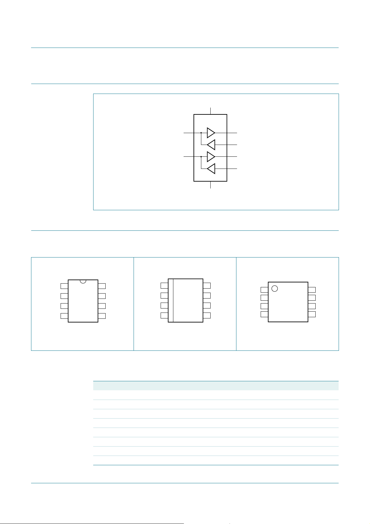
5. Block diagram
Sx (SDA)
Sy (SCL)
VCC (2 V to 15 V)
8
P82B96
1
7
4
3
2
5
6
P82B96
Dual bidirectional bus buffer
Tx (TxD, SDA)
Rx (RxD, SDA)
Ty (TxD, SCL)
Ry (RxD, SCL)
GND
002aab976
Fig 1. Block diagram of P82B96
6. Pinning information
6.1 Pinning
P82B96TD
P82B96TD/S900
1
1
Sx V
2
Rx Sy
P82B96PN
3
Tx Ry
4
GND Ty
002aab977
8
7
6
5
CC
Sx V
2
Rx Sy
3
Tx Ry
4
GND Ty
002aab978
Fig 2. Pin configuration for DIP8 Fig 3. Pin configuration for SO8 Fig 4. Pin configuration for
6.2 Pin description
8
CC
7
6
5
1
Sx V
2
Rx Sy
Tx Ry
GND Ty
3
4
P82B96DP
002aab979
TSSOP8
8
CC
7
6
5
Table 3. Pin description
Symbol Pin Description
2
Sx 1 I
C-bus (SDA or SCL)
Rx 2 receive signal
Tx 3 transmit signal
GND 4 negative supply
Ty 5 transmit signal
Ry 6 receive signal
2
Sy 7 I
V
CC
P82B96_8 © NXP B.V. 2009. All rights reserved.
Product data sheet Rev. 08 — 10 November 2009 3 of 32
8 positive supply voltage
C-bus (SDA or SCL)
Page 4

NXP Semiconductors
7. Functional description
Refer to Figure 1 “Block diagram of P82B96”.
The P82B96 has two identical buffers allowing buffering of both of the I2C-bus (SDA and
SCL) signals. Each buffer is made up of two logic signal paths, a forward path from the
I2C-bus interface pin which drives the buffered bus, and a reverse signal path from the
buffered bus input to drive the I2C-bus interface. Thus these paths are:
P82B96
Dual bidirectional bus buffer
• sense the voltage state of the I
Tx (Ty respectively), and
• sense the state of the pin Rx (Ry) and pull the I
LOW.
The rest of this discussion will address only the ‘x’ side of the buffer; the ‘y’ side is
identical.
The I2C-bus pin (Sx) is designed to interface with a normal I2C-bus.
The logic threshold voltage levels on the I2C-bus are independent of the IC supply VCC.
The maximum I2C-bus supply voltage is 15 V and the guaranteed static sink current is
3 mA.
The logic level of Rx is determined from the power supply voltage VCC of the chip. Logic
LOW is below 42 % of VCC, and logic HIGH is above 58 % of VCC(with a typical switching
threshold of half VCC).
Tx is an open-collector output without ESD protection diodes to VCC. It may be connected
via a pull-up resistor to a supply voltage in excess of VCC, as long as the 15 V rating is not
exceeded. It has a larger current sinking capability than a normal I2C-bus device, being
able to sink a static current of greater than 30 mA, and typical 100 mA dynamic pull-down
capability as well.
A logic LOW is only transmitted to Tx when the voltage at the I2C-bus pin (Sx) is below
0.6 V. A logic LOW at Rx will cause the I2C-bus (Sx) to be pulled to a logic LOW level in
accordance with I2C-bus requirements (maximum 1.5 V in 5 V applications) but not low
enough to be looped back to the Tx output and cause the buffer to latch LOW.
2
C-bus pin Sx (or Sy) and transmit this state to the pin
2
C-bus pin LOW whenever Rx (Ry) is
The minimum LOW level this chip can achieve on the I2C-bus by a LOW at Rx is typically
0.8 V.
If the supply voltageVCCfails,thenneithertheI2C-bus nor the Tx output willbeheldLOW.
Their open-collector configuration allows them to be pulled up to the rated maximum of
15 V even without VCC present. The input configuration on Sx and Rx also present no
loading of external signals even when VCC is not present.
The effectiveinput capacitance of any signal pin, measured by its effectonbusrise times,
is less than 7 pF for all bus voltages and supply voltages including VCC=0V.
Remark: Two or more Sx or Sy I/Os must not be interconnected. The P82B96 design
does not support this configuration. Bidirectional I2C-bus signals do not allow any
direction control pin so,instead,slightlydifferent logic low voltage levels are used at Sx/Sy
to avoid latching of this buffer. A ‘regular I2C-bus LOW’ applied at the Rx/Ry of a P82B96
will be propagated to Sx/Sy as a ‘buffered LOW’ with a slightly higher voltage level. If this
P82B96_8 © NXP B.V. 2009. All rights reserved.
Product data sheet Rev. 08 — 10 November 2009 4 of 32
Page 5

NXP Semiconductors
special ‘buffered LOW’ is applied to the Sx/Sy of another P82B96 that second P82B96 will
not recognize it as a ‘regular I2C-bus LOW’ and will not propagate it to its Tx/Ty output.
The Sx/Sy side of P82B96 may not be connected to similar buffers that rely on special
logic thresholds for their operation, for example PCA9511, PCA9515, or PCA9518. The
Sx/Sy side is only intended for, and compatible with, the normal I2C-bus logic voltage
levels of I2C-bus master and slave chips, or even Tx/Rx signals of a second P82B96 if
required. The Tx/Rx and Ty/Ry I/O pins use the standard I2C-bus logic voltage levels of all
I2C-bus parts. There are no restrictions on the interconnection of the Tx/Rx and Ty/Ry I/O
pins to other P82B96s, for example in a star or multipoint configuration with the Tx/Rx and
Ty/Ry I/O pins on the common bus and the Sx/Sy side connected to the line card slave
devices. For more details see
8. Limiting values
Table 4. Limiting values
In accordance with the Absolute Maximum Rating System (IEC 60134).
Voltages with respect to pin GND.
Symbol Parameter Conditions Min Max Unit
V
CC
V
Sx
V
Tx
V
Rx
I
n
P
tot
T
j
T
stg
T
amb
[1] See also Section 10.2 “Negative undershoot below absolute minimum value”.
P82B96
Dual bidirectional bus buffer
Application Note AN255
supply voltage VCC to GND −0.3 +18 V
voltage on pin Sx I2C-bus SDA or SCL −0.3 +18 V
voltage on pin Tx buffered output
voltage on pin Rx receive input
current on any pin - 250 mA
total power dissipation - 300 mW
junction temperature operating range
P82B96TD/S900
storage temperature −55 +125 °C
ambient temperature operating −40 +85 °C
.
[1]
−0.3 +18 V
[1]
−0.3 +18 V
−40 +125 °C
P82B96_8 © NXP B.V. 2009. All rights reserved.
Product data sheet Rev. 08 — 10 November 2009 5 of 32
Page 6
NXP Semiconductors
9. Characteristics
Table 5. Characteristics
T
= +25°C; voltages are specified with respect to GND with VCC= 5 V, unless otherwise specified.
amb
Symbol Parameter Conditions T
Min Typ Max Min Max
Power supply
V
CC
I
CC
supply voltage operating 2.0 - 15 2.0 15 V
supply current buses HIGH - 0.9 1.8 - 3 mA
=15V;
V
CC
buses HIGH
∆I
CC
additional quiescent
per Tx or Ty LOW - 1.7 3.5 - 3.5 mA
supply current
Bus pull-up (load) voltages and currents
, V
V
Sx
maximum input/output
Sy
voltage
open-collector;
2
I
C-busandVRx,VRy=
HIGH
, I
I
Sx
Sy
, I
I
Sx
Sy
, I
I
Sx
Sy
, V
V
Tx
static output loading on
2
I
C-bus
dynamic output sink
capability on I
leakage current on
2
I
C-bus
maximumoutputvoltage
Ty
2
C-bus
, VSy= 1.0 V;
V
Sx
V
Rx,VRy
V
Sx
V
Rx,VRy
V
Sx
V
Rx,VRy
V
Sx
V
Rx,VRy
=LOW
, VSy=2V;
=LOW
, VSy=5V;
= HIGH
, VSy=15V;
= HIGH
open-collector - - 15 - 15 V
[2]
0.2 - 3 0.2 3 mA
718- 7 -mA
level
, I
I
Tx
Ty
, I
I
Tx
Ty
, I
I
Tx
Ty
static output loading on
buffered bus
dynamic output sink
capability, buffered bus
leakage current on
buffered bus
VTx, VTy= 0.4 V;
V
2
I
= LOW on
Sx,VSy
C-bus = 0.4 V
VTx, VTy>1V;
V
2
I
= LOW on
Sx,VSy
C-bus = 0.4 V
VTx, VTy=VCC=15V;
V
, VSy= HIGH
Sx
60 100 - 60 - mA
Input currents
, I
I
Sx
Sy
, I
I
Rx
Ry
, I
I
Rx
Ry
input current from
2
I
C-bus
input current from
buffered bus
leakage current on
bus LOW;
VRx,VRy= HIGH
bus LOW;
V
Rx,VRy
VRx, VRy=V
= 0.4 V
CC
buffered bus input
Output logic LOW level
V
dV
dV
, V
Sx
Sx
Sy
output logic level LOW
Sy
on normal I
/dT,
temperature coefficient
/dT
of output LOW levels
2
C-bus
, ISy=3mA
I
Sx
, ISy= 0.2 mA
I
Sx
, ISy= 0.2 mA
I
Sx
[3]
0.8 0.88 1.0 (see Figure 6)V
[3]
670 730 790 (see Figure 5)mV
[3]
= +25 °C T
amb
- 1.1 2.5 - 4 mA
--15-15V
--1 -10µA
-1- - 10µA
- - 30 - 30 mA
-1- - 10µA
- −1- - −10 µA
- −1- - −10 µA
-1- - 10µA
- −1.8 - - - mV/K
P82B96
Dual bidirectional bus buffer
= −40 °C to
amb
+125 °C
[1]
Unit
P82B96_8 © NXP B.V. 2009. All rights reserved.
Product data sheet Rev. 08 — 10 November 2009 6 of 32
Page 7

NXP Semiconductors
P82B96
Dual bidirectional bus buffer
Table 5. Characteristics
T
= +25°C; voltages are specified with respect to GND with VCC= 5 V, unless otherwise specified.
amb
Symbol Parameter Conditions T
…continued
= +25 °C T
amb
Min Typ Max Min Max
Input logic switching threshold voltages
, V
V
Sx
, V
V
Sx
input logic voltage LOW on normal I2C-bus
Sy
input logic level HIGH
Sy
on normal I2C-bus
[4]
- 640 600 (see Figure 7)mV
[4]
700 650 - (see Figure 8)mV
threshold
/dT,
dV
dV
V
V
V
Rx
Rx
Rx
Sx
Sy
, V
, V
, V
temperature coefficient
/dT
of input thresholds
input logic HIGH level fraction of applied V
Ry
input threshold fraction of applied V
Ry
input logic LOW level fraction of applied V
Ry
CC
CC
CC
- −2 - - - mV/K
0.58V
- 0.5V
- - 0.58V
CC
CC
- - 0.42V
Logic level threshold difference
, V
V
Sx
input/output logic level
Sy
difference
VSx output LOW at
0.2 mA − V
Sx
input
[2]
50 85 - 50 - mV
HIGH maximum
Thermal resistance
R
th(j-pcb)
thermal resistance from
junctiontoprinted-circuit
board
SOT96-1 (SO8);
average lead
temperature at board
- 127 - - - K/W
interface
Bus release on V
V
V
Sx
Tx
, VSy,
, V
VCC voltage at which all
busesare guaranteed to
Ty
failure
CC
- - 1 (see Figure 9)V
be released
dV/dT temperature coefficient
- −4 - - - mV/K
of guaranteed release
voltage
Buffer response time
T
fall delay
VSxtoVTx,
V
to V
Sy
buffer time delay on
falling input between
V
Ty
Sx
threshold, and V
[5]
= input switching
Tx
R
pull-up = 160 Ω;
Tx
no capacitive load;
V
=5V
CC
-70- - -ns
output falling 50 %
T
rise delay
VSxtoVTx,
V
to V
Sy
Ty
buffer time delay on
rising input between
V
= input switching
Sx
threshold, and V
Tx
RTx pull-up = 160 Ω;
no capacitive load;
V
=5V
CC
-90- - -ns
output reaching 50 %
V
CC
= −40 °C to
amb
+125 °C
CC
[1]
Unit
-V
---V
CC
- 0.42VCCV
P82B96_8 © NXP B.V. 2009. All rights reserved.
Product data sheet Rev. 08 — 10 November 2009 7 of 32
Page 8

NXP Semiconductors
P82B96
Dual bidirectional bus buffer
Table 5. Characteristics
T
= +25°C; voltages are specified with respect to GND with VCC= 5 V, unless otherwise specified.
amb
Symbol Parameter Conditions T
…continued
= +25 °C T
amb
= −40 °C to
amb
+125 °C
[1]
Unit
Min Typ Max Min Max
T
fall delay
VRx to
V
, V
Sx
to V
Sy
buffer time delay on
falling input between
V
Ry
= input switching
Rx
threshold, and V
Sx
R
pull-up = 1500 Ω;
Sx
no capacitive load;
V
=5V
CC
- 250 - - - ns
output falling 50 %
T
rise delay
VRx to
V
, V
Sx
to V
Sy
buffer time delay on
rising input between
V
Ry
= input switching
Rx
threshold, and V
RSx pull-up = 1500 Ω;
- 270 - - - ns
no capacitive load;
V
=5V
CC
Sx
output reaching 50 %
V
CC
Input capacitance
C
i
input capacitance effective input
--7 - 7pF
capacitance of any
signal pin measured
by incremental bus
rise times
[1] Limit data for +125 °C applies to P82B96TD/S900 version. It is guaranteed by design/characterization, but not by 100 % test.
[2] The minimum value requirement for pull-up current, 200 µA, guarantees that the minimum value for VSxoutput LOW will always exceed
the minimum VSxinput HIGH level to eliminate any possibility of latching. The specified difference is guaranteed by design within any IC.
While the tolerances on absolute levels allow a small probability the LOW from one Sx output is recognized by an Sx input of another
P82B96, this has no consequences for normal applications. In any design the Sx pins of different ICs should never be linked because
the resulting system would be very susceptible to induced noise and would not support all I2C-bus operating modes.
[3] The output logic LOW depends on the sink current. For scaling, see
[4] The input logic threshold is independent of the supply voltage.
[5] The fall time of VTx from 5 V to 2.5 V in the test is approximately 15 ns.
The fall time of VSx from 5 V to 2.5 V in the test is approximately 50 ns.
The rise time of VTx from 0 V to 2.5 V in the test is approximately 20 ns.
The rise time of VSx from 0.9 V to 2.5 V in the test is approximately 70 ns.
Application Note AN255
.
P82B96_8 © NXP B.V. 2009. All rights reserved.
Product data sheet Rev. 08 — 10 November 2009 8 of 32
Page 9
NXP Semiconductors
P82B96
Dual bidirectional bus buffer
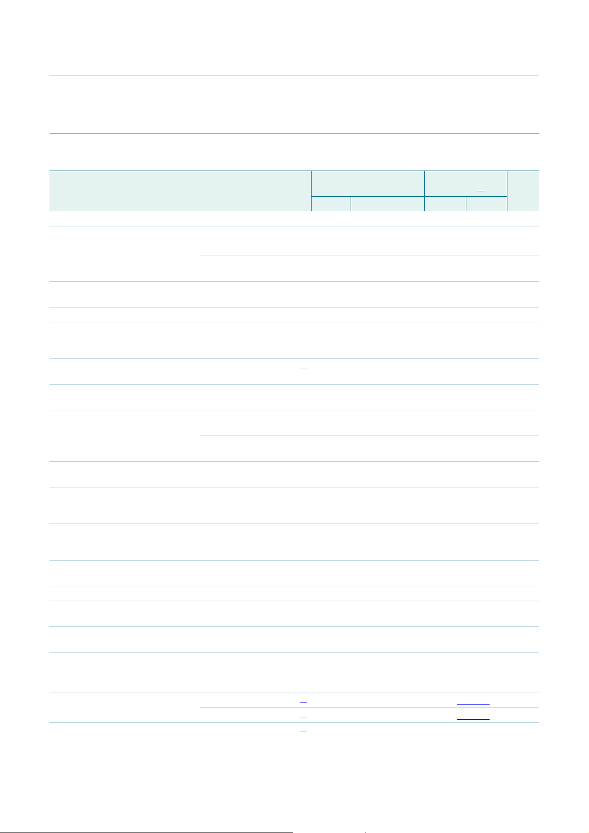
1000
V
OL
(mV)
800
600
400
−50 1251007550250−25
002aac069
(1)
(2)
(3)
T
(°C)
j
VOL at Sx typical and limits over temperature
(1) Maximum
(2) Typical
(3) Minimum
Fig 5. VOL as a function of junction temperature
(I
= 0.2 mA)
OL
1000
V
IL(max)
(mV)
800
002aac071
1200
V
OL
(mV)
1000
800
600
400
−50 1251007550250−25
(1) Maximum
(2) Typical
(3) Minimum
Fig 6. V
1000
V
IH(min)
(mV)
800
002aac070
T
(°C)
j
VOL at Sx typical and limits over temperature
as a function of junction temperature
OL
(I
= 3 mA)
OL
002aac072
(1)
(2)
(3)
600
400
200
−50 1251007550250−25
Fig 7. V
T
(°C)
j
V
at Sx changes over temperature range V
IL(max)
as a function of junction temperature Fig 8. V
IL(max)
1400
V
CC(max)
(mV)
1200
1000
800
600
400
−50 1251007550250−25
600
400
200
−50 1251007550250−25
at Sx changes over temperature range
IH(min)
as a function of junction temperature
IH(min)
002aac075
T
(°C)
j
T
(°C)
j
Fig 9. V
P82B96_8 © NXP B.V. 2009. All rights reserved.
that guarantees bus release limit over temperature
CC(max)
Product data sheet Rev. 08 — 10 November 2009 9 of 32
Page 10
NXP Semiconductors
10. Application information
P82B96
Dual bidirectional bus buffer
Refer to
AN460
and
AN255
I2C-bus
SDA
for more application detail.
+VCC (2 V to 15 V)
+5 V
Tx
(SDA)
Rx
(SDA)
1
/
P82B96
2
R1
'SDA' (new levels)
Fig 10. Interfacing an ‘I2C’ type of bus with different logic levels
I2C-bus
SDA
R1
+5 V
1
/
P82B96
2
R2
Rx
(SDA)
Tx
(SDA)
+V
CC
R3
+V
R4
002aab986
CC1
R5
I2C-bus
SDA
002aab987
2
Fig 11. Galvanic isolation of I
main enclosure
3.3 V to 5 V
SDA
SCL
Fig 12. Long distance I
P82B96_8 © NXP B.V. 2009. All rights reserved.
12 V
P82B96
2
C-bus nodes via opto-couplers
long cables
12 V3.3 V to 5 V
C-bus communications
remote control enclosure
3.3 V to 5 V
12 V
3.3 V to 5 V
P82B96
SDA
SCL
002aab988
Product data sheet Rev. 08 — 10 November 2009 10 of 32
Page 11

NXP Semiconductors
Figure 13 shows how a master I2C-bus can be protected against short circuits or failures
in applications that involve plug and socket connections and long cables that may become
damaged. A simple circuit is added to monitor the SDA bus, and if its LOW time exceeds
the design value, then the master bus is disconnected. P82B96 will free all its I/Os if its
supply is removed, so one option is to connect its VCC to the output of a logic gate from,
say, the 74LVC family. The SDA and SCL lines could be timed and VCC disabled via the
gate if one or other lines exceeds a design value of ‘LOW’ period as in
AN255
low-cost discrete circuit in Figure 13 can be used. If the SDA line is held LOW, the 100 nF
capacitor will charge and the Ry input will be pulled towards VCC. When it exceeds 0.5V
the Ry input will set the Sy input HIGH, which in practice means simply releasing it.
In this example the SCL line is made unidirectional by tying the Rx pin to VCC. The state of
the buffered SCL line cannot affect the master clock line which is allowed when
clock-stretching is not required. It is simple to add an additional transistor or diode to
control the Rx input in the same way as Ry when necessary. The +V cable drive can be
any voltage up to 15 V and the bus may be run at a lower impedance by selecting pull-up
resistors for a static sink current up to 30 mA. V
connected devices. Because DDC uses relatively low speeds (< 100 kHz), the cable
length is not restricted to 20 m by the I2C-bus signalling, but it may be limited by the video
signalling.
P82B96
Dual bidirectional bus buffer
Figure 28 of
. If the supply voltage of logic gates restricts the choice of VCC supply then the
CC1
and V
may be chosen to suit the
CC2
CC
V
CC1
V
CC
Rx
SCL
I2C-bus/DDC
master
SDA
GND
Sx
Sy
P82B96
PC/TV receiver/decoder box
Tx
Ry
Ty
470 kΩ
470 kΩ
Fig 13. Extending a DDC bus
100 nF
BC
847B
4.7 kΩ
+V cable drive
100
kΩ
BC
847B
3 m to 20 m
cables
I2C-bus/DDC
R
G
B
video signals
+V cable drive
Rx
Tx
Ry
Ty
P82B96
monitor/flat TV
V
CC2
V
CC
Sx
Sy
SCL
2
I
C-bus/DDC
slave
SDA
GND
002aab989
P82B96_8 © NXP B.V. 2009. All rights reserved.
Product data sheet Rev. 08 — 10 November 2009 11 of 32
Page 12

NXP Semiconductors
Figure 14 shows that P82B96 can achieve high clock rates over long cables. While
calculating with lumped wiring capacitance yields reasonable approximations to actual
timing, even 25 meters of cable is better treated using transmission line theory.Flat ribbon
cables connected as shown, with the bus signals on the outer edge, will have a
characteristic impedance in the range 100 Ω to 200 Ω. For simplicity they cannot be
terminated in their characteristic impedance but a practical compromise is to use the
minimum pull-up allowed for P82B96 and place half this termination at each end of the
cable. When each pull-up is below 330 Ω, the rising edge waveforms have their first
voltage ‘step’ level above the logic threshold at Rx and cable timing calculations can be
based on the fast rise/fall times of resistive loading plus simple one-way propagation
delays. When the pull-up is larger, but below 750 Ω, the threshold at Rx will be crossed
after one signal reflection. So at the sending end it is crossed after 2 times the one-way
propagation delay and at the receiving end after 3 times that propagation delay. For flat
cables with partial plastic dielectric insulation (by using outer cores) the one-way
propagation delays will be about 5 ns per meter. The 10 % to 90 % rise and fall times on
the cable will be between 20 ns and 50 ns, so their delay contributions are small. There
will be ringing on falling edges that can be damped, if required, by using Schottky diodes
as shown.
P82B96
Dual bidirectional bus buffer
When the Master SCL HIGH and LOW periods can be programmed separately, for
example using control registers I2SCLH and I2SCLL of 89LPC932, the timings can allow
for bus delays. The LOW period should be programmed to achieve the minimum 1300 ns
plus the net delay in the slave's response data signal caused by bus and buffer delays.
The longest data delay is the sum of the delay of the falling edge of SCL from master to
slave and the delay of the rising edge of SDA from slave data to master. Because the
buffer will ‘stretch’ the programmed SCL LOW period, the actual SCL frequency will be
lower than calculated from the programmed clock periods. In the example for 25 meters
the clock is stretched 400 ns, the falling edge of SCL is delayed 490 ns and the SDA rising
edge is delayed 570 ns. The required additional LOW period is
(490 ns + 570 ns) = 1060 ns and the I2C-bus specifications already include an allowance
for a worst case bus rise time 0 % to 70 % of 425 ns. (The bus rise time can be 300 ns
30 % to 70 %, which means it can be 425 ns 0 % to 70 %. The 25 meter cable delay times
as quoted already include all rise and fall times.) Therefore, the microcontroller only needs
to be programmed with an additional (1060 ns − 400 ns − 425 ns) = 235 ns, making a
total programmed LOW period 1535 ns. The programmed LOW will the be stretched by
400 ns to yield an actual bus LOW time of 1935 ns, which, allowing the minimum HIGH
period of 600 ns, yields a cycle period of 2535 ns or 394 kHz.
Note that in both the 100 meter and 250 meter examples, the capacitive loading on the
I2C-buses at each end is within the maximum allowed Standard mode loading of 400 pF,
but exceeds the Fast mode limit. This is an example of a ‘hybrid’ mode because it relies on
the response delays of Fast mode parts but uses (allowable) Standard mode bus loadings
with rise times that contribute significantly to the system delays. The cables cause large
propagation delays, so these systems need to operate well below the 400 kHz limit, but
illustrate how they can still exceed the 100 kHz limit provided all parts are capable of
Fast mode operation. The fastest example illustrates how the 400 kHz limit can be
exceeded, provided masters and slaves have the required timings, namely smaller than
the maximum allowed for Fast mode. Many NXP slaves have delays shorter than 600 ns
and all Fm+ devices must be < 450 ns.
P82B96_8 © NXP B.V. 2009. All rights reserved.
Product data sheet Rev. 08 — 10 November 2009 12 of 32
Page 13

NXP Semiconductors
P82B96
Dual bidirectional bus buffer
CC
+V cable drive
Rx
Tx
Ry
Ty
R1 R1
V
CC1
I2C-BUS
MASTER
SCL
SDA
R2
R2
Sx
Sy
V
P82B96
C2C2
GND
BAT54A
Fig 14. Driving ribbon or flat telephone cables
cable
propagation
delay ≈ 5 ns/m
R1 R1
BAT54A
Rx
Tx
Ry
Ty
V
P82B96
CC
Sx
Sy
V
CC2
R2
R2
SCL
2
I
C-BUS
SLAVE(S)
SDA
C2C2
GND
002aab990
P82B96_8 © NXP B.V. 2009. All rights reserved.
Product data sheet Rev. 08 — 10 November 2009 13 of 32
Page 14

xxxxxxxxxxxxxxxxxxxxx xxxxxxxxxxxxxxxxxxxxxxxxxx xxxxxxx x x x xxxxxxxxxxxxxxxxxxxxxxxxxxxxxx xxxxxxxxxxxxxxxxxxx xx xx
xxxxx xxxxxxxxxxxxxxxxxxxxxxxxxxx xxxxxxxxxxxxxxxxxxx xxxxxx xxxxxxxxxxxxxxxxxxxxxxxxxxxxxxxxxxx xxxxxxxxxxxx x x
xxxxxxxxxxxxxxxxxxxxx xxxxxxxxxxxxxxxxxxxxxxxxxxxxxx xxxxx xxxxxxxxxxxxxxxxxxxxxxxxxxxxxxxxxxxxxxxxxxxxxxxxxx xxxxxxxx
P82B96_8 © NXP B.V. 2009. All rights reserved.
Product data sheet Rev. 08 — 10 November 2009 14 of 32
Table 6. Examples of bus capability
Refer to Figure 14.
+V
CC1
5 V 12 V 5 V 750 2.2 k 400 250 m n/a
5 V 12 V 5 V 750 2.2 k 220 100 m n/a
3.3 V 5 V 3.3 V 330 1 k 220 25 m 1 nF 125 ns 600 ns 1500 ns 390 kHz Normal spec.
3.3 V 5 V 3.3 V 330 1 k 100 3 m 120 pF 15 ns 600 ns 1000 ns 500 kHz 600 ns
xxxxxxxxxxxxxxxxxxxxxxxxx xxxxxxxxxxxxxxxxxxxx xxx
+V
cable
+V
R1
CC2
(Ω)R2(Ω)C2(pF)
Cable
length
Cable
capacitance
(delay based)
(delay based)
Cable
delay
1.25 µs 600 ns 4000 ns 120 kHz Normal spec.
500 ns 600 ns 2600 ns 185 kHz Normal spec.
Set master nominal SCL Effective
HIGH period LOW period
bus clock
speed
NXP Semiconductors
Maximum slave
response delay
400 kHz parts
400 kHz parts
400 kHz parts
Dual bidirectional bus buffer
P82B96
Page 15

NXP Semiconductors
10.1 Calculating system delays and bus clock frequency for a Fast mode
system
P82B96
Dual bidirectional bus buffer
local master bus
V
CCM
Rm
MASTER
2
I
C-BUS
SCL
GND (0 V)
Effective delay of SCL at slave: 255 + 17V
V
CCB
Sx
Cm
master bus
capacitance
P82B96 P82B96
CCM
buffered expansion bus
Rb Rs
Tx/Rx
Tx/Rx Sx
Cb
buffered bus
wiring capacitance
+ (2.5 + 4 × 10⁹ Cb)V
CCB
+ 10V
CCS
ns.
C = F; V = volts.
Fig 15. Falling edge of SCL at master is delayed by the buffers and bus fall times
V
CCM
local master bus
V
CCB
buffered expansion bus
remote slave bus
SCL
Cs
slave bus
capacitance
SLAVE
I2C-BUS
V
CCS
002aab991
MASTER
2
I
C-BUS
SCL
GND (0 V)
Rm
Sx
Cm
master bus
capacitance
P82B96
Tx/Rx
Rb
Tx/Rx
Cb
buffered bus
wiring capacitance
002aab992
Effective delay of SCL at master: 270 + RmCm + 0.7RbCb ns.
C = F; R = Ω.
Fig 16. Rising edge of SCL at master is delayed (clock stretch) by buffer and bus rise times
P82B96_8 © NXP B.V. 2009. All rights reserved.
Product data sheet Rev. 08 — 10 November 2009 15 of 32
Page 16

NXP Semiconductors
P82B96
Dual bidirectional bus buffer
local master bus
V
CCM
MASTER
2
I
C-BUS
Effective delay of SDA at master = 270 + 0.2RsCs + 0.7 (RbCb + RmCm) ns.
C = F; R = Ω.
SDA
GND (0 V)
V
CCB
Rm
Sx
Cm
master bus
capacitance
P82B96 P82B96
buffered expansion bus
Rb Rs
Tx/Rx
Tx/Rx Sx
Cb
buffered bus
wiring capacitance
Fig 17. Rising edge of SDA at slave is delayed by the buffers and bus rise times
Figure 15, Figure 16, and Figure 17 show the P82B96 used to drive extended bus wiring,
with relatively large capacitance, linking two Fast mode I2C-bus nodes. It includes
simplified expressions for making the relevant timing calculations for 3.3 V or 5 V
operation. Because the buffers and the wiring introduce timing delays, it may be
necessary to decrease the nominal SCL frequency below 400 kHz. In most cases the
actual bus frequency will be lower than the nominal Master timing due to bit-wise
stretching of the clock periods.
remote slave bus
SDA
Cs
slave bus
capacitance
SLAVE
I2C-BUS
V
CCS
002aab993
The delay factors involved in calculation of the allowed bus speed are:
A — The propagation delay of the master signal through the buffers and wiring to the
slave. The important delay is that of the falling edge of SCL because this edge ‘requests’
the data or acknowledge from a slave. See Figure 15.
B — The effective stretching of the nominal LOW period of SCL at the master caused by
the buffer and bus rise times. See Figure 16.
C — The propagation delay of the slave's response signal through the buffers and wiring
back to the master. The important delay is that of a rising edge in the SDA signal. Rising
edges are always slower and are therefore delayed by a longer time than falling edges.
(The rising edges are limited by the passive pull-up while falling edges are actively driven).
See Figure 17.
The timing requirement in any I2C-bus system is that a slave's data response (which is
provided in response to a falling edge of SCL) must be received at the master before the
end of the corresponding LOW period of SCL as appears on the bus wiring at the master.
Since all slaves will, as a minimum, satisfy the worst case timing requirements of a
400 kHz part, they must provide their response within the minimum allowed clock LOW
period of 1300 ns. Therefore in systems that introduce additional delays it is only
necessary to extend that minimum clock LOW period by any ‘effective’ delay of the slave's
response. The effectivedelay of the slaves response equals the total delays in SCL falling
P82B96_8 © NXP B.V. 2009. All rights reserved.
Product data sheet Rev. 08 — 10 November 2009 16 of 32
Page 17

NXP Semiconductors
edge from the master reaching the slave (Figure 15) minus the effective delay (stretch) of
the SCL rising edge (Figure 16) plus total delays in the slave's response data, carried on
SDA, reaching the master (Figure 17).
The master microcontroller should be programmed to produce a nominal SCL LOW
period = (1300 + A − B + C) ns, and should be programmed to produce the nominal
minimum SCL HIGH period of 600 ns. Then a check should be made to ensure the cycle
time is not shorter than the minimum 2500 ns. If found necessary, just increase either
clock period.
Due to clock stretching, the SCL cycle time will always be longer than
(600+1300+A+C)ns.
Example:
P82B96
Dual bidirectional bus buffer
SDA
SCL
3.3 V to 5 V
3.3 V to 5 V
The master bus has an RmCm product of 100 ns and V
CCM
=5V.
The bufferedbus has a capacitance of 1 nF and a pull-up resistor of 160 Ω to 5 V giving
an RbCb product of 160 ns. The slave bus also has an RsCs product of 100 ns.
The microcontroller LOW period should be programmed to
≥ (1300 + 372.5 − 482 + 472) ns, that is ≥ 1662.5 ns.
Its HIGH period may be programmed to the minimum 600 ns.
The nominal microcontroller clock period will be ≥ (1662.5 + 600) ns = 2262.5 ns,
equivalent to a frequency of 442 kHz.
The actual bus clock period, including the 482 ns clock stretch effect, will be below
(nominal + stretch) = (2262.5 + 482) ns or ≥ 2745 ns, equivalent to an allowable
frequency of 364 kHz.
12 V
Sx
Sy
P82B96
Tx
Rx
Ty
Ry
12 V
12 V
P82B96
Sx Sy
SCL/SDA
no limit to the number of connected bus devices
P82B96
Sx Sy
SCL/SDA
P82B96
Sx Sy
SCL/SDA
P82B96
twitsted-pair telephone wires,
USB, or flat ribbon cables;
up to 15 V logic levels,
include V
3.3 V 3.3 V
and GND
CC
Sy SDA
Sx SCL
002aab994
Fig 18. I2C-bus multipoint application
P82B96_8 © NXP B.V. 2009. All rights reserved.
Product data sheet Rev. 08 — 10 November 2009 17 of 32
Page 18

NXP Semiconductors
P82B96
Dual bidirectional bus buffer
14
V
10
6
2
−2
0 20001600800 1200400
Frequency = 624 kHz Ch1 frequency = 624 kHz
Tx
Sx
002aab995
ns
Fig 19. Propagation Sx to Tx (Sx pull-up to 5 V;
Tx pull-up to V
CC
=10V)
10.2 Negative undershoot below absolute minimum value
The reason why the IC pin reverse voltage on pins Tx and Rx in Table 4 “Limiting values”
is specified at such a low value, −0.3 V, is not that applying larger voltages is likely to
cause damage but that it is expected that, in normal applications, there is no reason why
larger DC voltages will be applied. This ‘absolute maximum’ specification is intended to be
a DC or continuous ratings and the nominal DC I2C-bus voltage LOW usually does not
even reach 0 V. Inside P82B96 at every pin there is a large protective diode connected to
the GND pin and that diode will start to conduct when the pin voltage is more than about
−0.55 V with respect to GND at 25 °C ambient.
14
V
10
6
2
−2
Rx
Sx
0 20001600800 1200400
002aab996
ns
Fig 20. Propagation Rx to Sx (Sx pull-up to 5 V;
Rx pull-up to VCC=10V)
Figure 21 shows the measured characteristic for one of those diodes inside P82B96. The
plot was made using a curve tracer that applies 50 Hz mains voltage via a series resistor,
so the pulse durations are long duration (several milliseconds) and are reaching peaks of
over 2 A when more than −1.5 V is applied. The IC becomes very hot during this testing
but it was not damaged. Whenever there is current flowing in any of these diodes it is
possible that there can be faulty operation of any IC. For that reason we put a specification
on the negative voltage that is allowed to be applied. It is selected so that, at the highest
allowed junction temperature, there will be a big safety factor that guarantees the diode
will not conduct and then we do not need to make any 100 % production tests to
guarantee the published specification.
For the P82B96, in specific applications, there will always be transient overshoot and
ringing on the wiring that can cause these diodes to conduct. Therefore we designed the
IC to withstand those transients and as a part of the qualification procedure we made
tests, using DC currents to more than twice the normal bus sink currents, to be sure that
the IC was not affected by those currents. For example, the Tx/Ty and Rx/Ry pins were
tested to at least −80 mA which, from Figure 21, would be more than −0.8 V. The correct
functioning of the P82B96 is not affected even by those large currents. The Absolute
Maximum (DC) ratings are not intended to apply to transients but to steady state
conditions. This explains why you will never see any problems in practice even if, during
transients, more than −0.3 V is applied to the bus interface pins of P82B96.
P82B96_8 © NXP B.V. 2009. All rights reserved.
Product data sheet Rev. 08 — 10 November 2009 18 of 32
Page 19

NXP Semiconductors
Figure 21 “Diode characteristic curve” also explains how the general Absolute Maximum
DC specification was selected. The current at 25 °C is near zero at −0.55 V. The P82B96
is allowed to operate with +125 °C junction and that would cause this diode voltage to
decrease by 100 × 2 mV = 200 mV. So for zero current we need to specify −0.35 V and we
publish −0.3 V just to have some extra margin.
Remark: You should not be concerned about the transients generated on the wiring by a
P82B96 in normal applications and that is input to the Tx/Rx or Ty/Ry pins of another
P82B96. Because not all ICs that may be driven by P82B96 are designed to tolerate
negative transients, in Section 10.2.1 “Example with questions and answers” we show
they can be managed if required.
P82B96
Dual bidirectional bus buffer
0
diode current
(mA)
−1
−10
−1
−10
2
−10
3
−10
4
−10
−2.0 0−0.5−1.5 −1.0
Fig 21. Diode characteristic curve
002aaf063
voltage (V)
P82B96_8 © NXP B.V. 2009. All rights reserved.
Product data sheet Rev. 08 — 10 November 2009 19 of 32
Page 20

NXP Semiconductors
10.2.1 Example with questions and answers
Question: On a falling edge of Tx we measure undershoot at −800 mV at the linked Tx,
Rx pins of the P82B96 that is generating the LOW,but the P82B96 data sheet specifies
minimum −0.3 V. Does this mean that we violate the data sheet absolute value?
Answer: For P82B96 the −0.3 V Absolute Maximum rating is not intended to apply to
transients, it is a DC rating. As shown in Figure 22, there is no theoretical reason for any
undershoot at the IC that is driving the bus LOW and no significant undershoot should
be observed when using reasonable care with the ground connection of the ‘scope. It is
more likely that undershoot observed at a driving P82B96 is caused by local stray
inductance and capacitance in the circuit and by the oscilloscope connections. As
shown, undershoot will be generated by PCB traces, wiring, or cables driven by a
P82B96 because the allowed value of the I2C-bus pull-up resistor generally is larger
than that required to correctly terminate the wiring. In this example, with no IC
connected at the end of the wiring, the undershoot is about 2 V.
voltage
(V)
P82B96
Dual bidirectional bus buffer
6
4
send
2
0
−2
horizontal scale = 62.5 ns/div
Sx
5 V
Rx
Tx
P82B96
5 V
300 Ω
send
Fig 22. Transients generated by the bus wiring
receive
2 meter
cable
time (ns)
5 V
300 Ω
receive
GND
002aaf064
P82B96_8 © NXP B.V. 2009. All rights reserved.
Product data sheet Rev. 08 — 10 November 2009 20 of 32
Page 21

NXP Semiconductors
Question: We have 2 meters of cable in a bus that joins the Tx/Rx sides of two P82B96
devices. When one Tx drives LOW the other P82B96 Tx/Rx is driven to −0.8 V for over
50 ns. What is the expected value and the theoretically allowed value of undershoot?
Answer: Because the cable joining the two P82B96s is a ‘transmission line’ that will
have a characteristic impedance around 100 Ω and it will be terminated by pull-up
resistors that are larger than that characteristic impedance there will always be negative
undershoot generated. The duration of the undershoot is a function of the cable length
and the input impedance of the connected IC. As shown in Figure 23, the transient
undershoot will be limited, by the diodes inside P82B96, to around −0.8 V and that will
not cause problems for P82B96. Those transients will not be passed inside the IC to the
Sx/Sy side of the IC.
P82B96
Dual bidirectional bus buffer
6
voltage
(V)
4
2
cable
receive
5 V
time (ns)
300 Ω
receive
GND
5 V
Rx
Sx
Tx
002aaf065
send
0
−2
horizontal scale = 62.5 ns/div
5 V
Sx
Rx
Tx
P82B96
5 V
300 Ω
send
2 meter
Fig 23. Wiring transients limited by the diodes in P82B96
Question: If we input 800 mV undershoot at Tx, Rx pins, what kind of problem is
expected?
Answer: When that undershoot is generated by another P82B96 and is simply the
result of the system wiring, then there will be no problems.
Question: Will we have any functional problem or reliability problem?
Answer: No.
P82B96_8 © NXP B.V. 2009. All rights reserved.
Product data sheet Rev. 08 — 10 November 2009 21 of 32
Page 22

NXP Semiconductors
Question: If we add 100 Ω to 200 Ω at signal line, the overshoot becomes slightly
smaller. Is this a good idea?
Answer: No, it is not necessary to add any resistance. When the logic signal generated
by Tx or Ty of P82B96 drives long traces or wiring with ICs other than P82B96 being
driven, then adding a Schottky diode (BAT54A) as shown in Figure 24 will clamp the
wiring undershoot to a value that will not cause conduction of the IC’s internal diodes.
P82B96
Dual bidirectional bus buffer
6
voltage
(V)
4
2
send
0
receive
−2
horizontal scale = 62.5 ns/div
Sx
5 V
Rx
Tx
P82B96
send
5 V
300 Ω
2 meter
cable
5 V
300 Ω
receive
1
/2 BAT54A
Fig 24. Wiring transients limited by a Schottky diode
time (ns)
5 V
Rx
Tx
GND
002aaf066
Sx
P82B96_8 © NXP B.V. 2009. All rights reserved.
Product data sheet Rev. 08 — 10 November 2009 22 of 32
Page 23

NXP Semiconductors
11. Package outline
P82B96
Dual bidirectional bus buffer
DIP8: plastic dual in-line package; 8 leads (300 mil)
D
seating plane
A
L
Z
e
b
8
pin 1 index
1
w M
b
1
b
2
5
SOT97-1
M
E
A
2
A
c
(e )
1
M
H
E
1
DIMENSIONS (inch dimensions are derived from the original mm dimensions)
A
A
12
min.
max.
050G01 MO-001 SC-504-8
b
1.73
1.14
0.068
0.021
0.045
0.015
IEC JEDEC JEITA
mm
OUTLINE
VERSION
SOT97-1
A
max.
UNIT
inches
Note
1. Plastic or metal protrusions of 0.25 mm (0.01 inch) maximum per side are not included.
b
0.53
0.38
4
0 5 10 mm
scale
1
1.07
0.89
0.042
0.035
b
2
0.36
0.23
0.014
0.009
REFERENCES
(1) (1)
cD E e M
9.8
9.2
0.39
0.36
6.48
6.20
0.26
0.24
1
3.60
3.05
0.14
0.12
E
8.25
7.80
0.32
0.31
EUROPEAN
PROJECTION
10.0
0.39
0.33
M
L
e
H
8.3
w
max.
0.2542.54 7.62
0.010.1 0.3
0.0450.17 0.02 0.13
ISSUE DATE
99-12-27
03-02-13
1.154.2 0.51 3.2
(1)
Z
Fig 25. Package outline SOT97-1 (DIP8)
P82B96_8 © NXP B.V. 2009. All rights reserved.
Product data sheet Rev. 08 — 10 November 2009 23 of 32
Page 24

NXP Semiconductors
P82B96
Dual bidirectional bus buffer
SO8: plastic small outline package; 8 leads; body width 3.9 mm
D
c
y
Z
8
pin 1 index
1
e
5
A
2
A
4
w M
b
p
SOT96-1
E
H
E
1
detail X
A
X
v M
A
Q
(A )
L
p
L
A
3
θ
0 2.5 5 mm
scale
DIMENSIONS (inch dimensions are derived from the original mm dimensions)
mm
OUTLINE
VERSION
SOT96-1
A
max.
1.75
0.069
A1A2A
0.25
1.45
0.10
1.25
0.010
0.057
0.004
0.049
IEC JEDEC JEITA
076E03 MS-012
0.25
0.01
b
3
p
0.49
0.25
0.36
0.19
0.019
0.0100
0.014
0.0075
UNIT
inches
Notes
1. Plastic or metal protrusions of 0.15 mm (0.006 inch) maximum per side are not included.
2. Plastic or metal protrusions of 0.25 mm (0.01 inch) maximum per side are not included.
(1)E(2)
cD
5.0
4.8
0.20
0.19
REFERENCES
eHELLpQZywv θ
4.0
3.8
0.16
0.15
1.27
0.05
6.2
5.8
0.244
0.228
1.05
1.0
0.4
0.039
0.016
0.7
0.6
0.028
0.024
0.25 0.10.25
0.010.010.041 0.004
EUROPEAN
PROJECTION
(1)
0.7
0.3
0.028
0.012
ISSUE DATE
99-12-27
03-02-18
o
8
o
0
Fig 26. Package outline SOT96-1 (SO8)
P82B96_8 © NXP B.V. 2009. All rights reserved.
Product data sheet Rev. 08 — 10 November 2009 24 of 32
Page 25

NXP Semiconductors
P82B96
Dual bidirectional bus buffer
TSSOP8: plastic thin shrink small outline package; 8 leads; body width 3 mm
D
y
Z
8
pin 1 index
5
14
e
w M
b
p
c
A
2
A
1
E
H
E
detail X
SOT505-1
A
X
v M
A
(A3)
L
p
L
A
θ
2.5 5 mm0
scale
DIMENSIONS (mm are the original dimensions)
A
A
UNIT
max.
mm
1.1
Notes
1. Plastic or metal protrusions of 0.15 mm maximum per side are not included.
2. Plastic or metal protrusions of 0.25 mm maximum per side are not included.
OUTLINE
VERSION
SOT505-1
1
0.15
0.05
A2A3b
0.95
0.25
0.80
IEC JEDEC JEITA
p
0.45
0.25
ceD
0.28
0.15
(1)E(2)
3.1
3.1
2.9
2.9
REFERENCES
0.65
5.1
4.7
LH
E
L
0.7
0.4
p
wyv
0.1 0.10.10.94
EUROPEAN
PROJECTION
(1)
Z
0.70
0.35
ISSUE DATE
θ
6°
0°
99-04-09
03-02-18
Fig 27. Package outline SOT505-1 (TSSOP8)
P82B96_8 © NXP B.V. 2009. All rights reserved.
Product data sheet Rev. 08 — 10 November 2009 25 of 32
Page 26

NXP Semiconductors
12. Soldering of SMD packages
This text provides a very brief insight into a complex technology. A more in-depth account
of soldering ICs can be found in Application Note
soldering description”
12.1 Introduction to soldering
Soldering is one of the most common methods through which packages are attached to
Printed Circuit Boards (PCBs), to form electrical circuits. The soldered joint provides both
the mechanical and the electrical connection. There is no single soldering method that is
ideal for all IC packages. Wave soldering is often preferred when through-hole and
Surface Mount Devices (SMDs) are mixed on one printed wiring board; however, it is not
suitable for fine pitch SMDs. Reflow soldering is ideal for the small pitches and high
densities that come with increased miniaturization.
12.2 Wave and reflow soldering
Wave soldering is a joining technology in which the joints are made by solder coming from
a standing wave of liquid solder. The wave soldering process is suitable for the following:
.
P82B96
Dual bidirectional bus buffer
AN10365 “Surface mount reflow
• Through-hole components
• Leaded or leadless SMDs, which are glued to the surface of the printed circuit board
Not all SMDs can be wave soldered. Packages with solder balls, and some leadless
packages which have solder lands underneath the body, cannot be wave soldered. Also,
leaded SMDs with leads having a pitch smaller than ~0.6 mm cannot be wave soldered,
due to an increased probability of bridging.
The reflow soldering process involves applying solder paste to a board, followed by
component placement and exposure to a temperature profile. Leaded packages,
packages with solder balls, and leadless packages are all reflow solderable.
Key characteristics in both wave and reflow soldering are:
• Board specifications, including the board finish, solder masks and vias
• Package footprints, including solder thieves and orientation
• The moisture sensitivity level of the packages
• Package placement
• Inspection and repair
• Lead-free soldering versus SnPb soldering
12.3 Wave soldering
Key characteristics in wave soldering are:
• Process issues, such as application of adhesive and flux, clinching of leads, board
transport, the solder wave parameters, and the time during which components are
exposed to the wave
• Solder bath specifications, including temperature and impurities
P82B96_8 © NXP B.V. 2009. All rights reserved.
Product data sheet Rev. 08 — 10 November 2009 26 of 32
Page 27

NXP Semiconductors
12.4 Reflow soldering
Key characteristics in reflow soldering are:
• Lead-freeversus SnPb soldering; note that a lead-free reflow process usually leads to
• Solder paste printing issues including smearing, release, and adjusting the process
• Reflow temperature profile; this profile includes preheat, reflow (in which the board is
Table 7. SnPb eutectic process (from J-STD-020C)
Package thickness (mm) Package reflow temperature (°C)
< 2.5 235 220
≥ 2.5 220 220
P82B96
Dual bidirectional bus buffer
higher minimum peak temperatures (see Figure 28) than a SnPb process, thus
reducing the process window
window for a mix of large and small components on one board
heated to the peak temperature) and cooling down. It is imperative that the peak
temperature is high enough for the solder to make reliable solder joints (a solder paste
characteristic). In addition, the peak temperature must be low enough that the
packages and/or boards are not damaged. The peak temperature of the package
depends on package thickness and volume and is classified in accordance with
Table 7 and 8
Volume (mm3)
< 350 ≥ 350
Table 8. Lead-free process (from J-STD-020C)
Package thickness (mm) Package reflow temperature (°C)
Volume (mm3)
< 350 350 to 2000 > 2000
< 1.6 260 260 260
1.6 to 2.5 260 250 245
> 2.5 250 245 245
Moisture sensitivity precautions, as indicated on the packing, must be respected at all
times.
Studies have shown that small packages reach higher temperatures during reflow
soldering, see Figure 28.
P82B96_8 © NXP B.V. 2009. All rights reserved.
Product data sheet Rev. 08 — 10 November 2009 27 of 32
Page 28

NXP Semiconductors
Fig 28. Temperature profiles for large and small components
maximum peak temperature
temperature
MSL: Moisture Sensitivity Level
= MSL limit, damage level
minimum peak temperature
= minimum soldering temperature
P82B96
Dual bidirectional bus buffer
peak
temperature
time
001aac844
For further information on temperature profiles, refer to Application Note
“Surface mount reflow soldering description”
.
13. Soldering of through-hole mount packages
13.1 Introduction to soldering through-hole mount packages
This text gives a very brief insight into wave, dip and manual soldering.
Wave soldering is the preferred method for mounting of through-hole mount IC packages
on a printed-circuit board.
13.2 Soldering by dipping or by solder wave
Driven by legislation and environmental forces the worldwide use of lead-free solder
pastes is increasing. Typical dwell time of the leads in the wave ranges from
3 seconds to 4 seconds at 250 °C or 265 °C, depending on solder material applied, SnPb
or Pb-free respectively.
The total contact time of successive solder waves must not exceed 5 seconds.
The device may be mounted up to the seating plane, but the temperature of the plastic
body must not exceed the specified maximum storage temperature (T
printed-circuit board has been pre-heated, forced cooling may be necessary immediately
after soldering to keep the temperature within the permissible limit.
AN10365
stg(max)
). If the
13.3 Manual soldering
Apply the soldering iron (24 V or less) to the lead(s) of the package, either below the
seating plane or not more than 2 mm above it. If the temperature of the soldering iron bit is
less than 300 °C it may remain in contact for up to 10 seconds. If the bit temperature is
between 300 °C and 400 °C, contact may be up to 5 seconds.
P82B96_8 © NXP B.V. 2009. All rights reserved.
Product data sheet Rev. 08 — 10 November 2009 28 of 32
Page 29

NXP Semiconductors
13.4 Package related soldering information
Table 9. Suitability of through-hole mount IC packages for dipping and wave soldering
Package Soldering method
CPGA, HCPGA - suitable
DBS, DIP, HDIP, RDBS, SDIP, SIL suitable suitable
PMFP
[1] For SDIP packages, the longitudinal axis must be parallel to the transport direction of the printed-circuit
[2] For PMFP packages hot bar soldering or manual soldering is suitable.
14. Abbreviations
Table 10. Abbreviations
Acronym Description
CDM Charged Device Model
DDC Display Data Channel
ESD ElectroStatic Discharge
HBM Human Body Model
IC Integrated Circuit
2
C-bus Inter IC bus
I
MM Machine Model
SMBus System Management Bus
[2]
board.
P82B96
Dual bidirectional bus buffer
Dipping Wave
[1]
- not suitable
P82B96_8 © NXP B.V. 2009. All rights reserved.
Product data sheet Rev. 08 — 10 November 2009 29 of 32
Page 30

NXP Semiconductors
Dual bidirectional bus buffer
15. Revision history
Table 11. Revision history
Document ID Release date Data sheet status Change notice Supersedes
P82B96_8 20091110 Product data sheet - P82B96_7
Modifications:
P82B96_7 20090212 Product data sheet - P82B96_6
P82B96_6 20080131 Product data sheet - P82B96_5
P82B96_5 20060127 Product data sheet - P82B96_4
P82B96_4
(9397 750 12932)
P82B96_3
(9397 750 11351)
P82B96_2
(9397 750 11093)
P82B96_1
(9397 750 08122)
• Table 4 “Limiting values”: added Table note [1].
• Added Section 10.2 “Negative undershoot below absolute minimum value”.
20040329 Product data - P82B96_3
20030402 Product data 853-2241 29602
of 2003 Feb 28
20030220 Product data 853-2241 29410
of 2003 Jan 22
20010306 Product data 853-2241 25758
of 2001 Mar 06
P82B96_2
P82B96_1
-
P82B96
P82B96_8 © NXP B.V. 2009. All rights reserved.
Product data sheet Rev. 08 — 10 November 2009 30 of 32
Page 31

NXP Semiconductors
16. Legal information
16.1 Data sheet status
P82B96
Dual bidirectional bus buffer
Document status
Objective [short] data sheet Development This document contains data from the objective specification for product development.
Preliminary [short] data sheet Qualification This document contains data from the preliminary specification.
Product [short] data sheet Production This document contains the product specification.
[1] Please consult the most recently issued document before initiating or completing a design.
[2] The term ‘short data sheet’ is explained in section “Definitions”.
[3] The product status of device(s) described in this document may have changed since this document was published and may differ in case of multiple devices.The latest product status
information is available on the Internet at URL
[1][2]
Product status
16.2 Definitions
Draft — The document is a draft version only. The content is still under
internal review and subject to formal approval, which may result in
modifications or additions. NXP Semiconductors does not give any
representations or warranties as to the accuracy or completeness of
information included hereinand shall have no liabilityfor the consequences of
use of such information.
Short data sheet — A short data sheet is an extract from a full data sheet
with the sameproduct type number(s) and title. Ashort data sheetis intended
for quickreference only and should not be relied upon to contain detailed and
full information. For detailed and full information see the relevant full data
sheet, which is available on request via the local NXP Semiconductors sales
office. In case of any inconsistency or conflict with the short data sheet, the
full data sheet shall prevail.
16.3 Disclaimers
General — Information in this document is believed to be accurate and
reliable. However,NXP Semiconductors does not give any representations or
warranties, expressedor implied, as to the accuracy or completeness of such
information and shall have no liability for the consequences of use of such
information.
Right to make changes — NXP Semiconductors reserves the right to make
changes to information published in this document, including without
limitation specifications and product descriptions, at any time and without
notice. This document supersedes and replaces all information supplied prior
to the publication hereof.
Suitability for use — NXP Semiconductors products are not designed,
authorized or warranted to be suitable for use in medical, military, aircraft,
space or life support equipment, nor in applications where failure or
malfunction of an NXP Semiconductors product can reasonably be expected
to result in personal injury, death or severe property or environmental
[3]
http://www.nxp.com.
Definition
damage. NXP Semiconductors accepts no liability for inclusion and/or use of
NXP Semiconductors products in such equipment or applications and
therefore such inclusion and/or use is at the customer’s own risk.
Applications — Applications that are described herein for any of these
products are for illustrative purposes only. NXP Semiconductors makes no
representation or warranty that such applications will be suitable for the
specified use without further testing or modification.
Limiting values — Stress above one or more limiting values (as defined in
the Absolute Maximum Ratings System of IEC 60134) maycause permanent
damage to the device.Limiting values are stress ratings onlyand operation of
the device at these or any other conditions above those given in the
Characteristics sections of this document is not implied. Exposure to limiting
values for extended periods may affect device reliability.
Terms and conditions of sale — NXP Semiconductors products are sold
subject to the general terms and conditions of commercial sale, as published
at
http://www.nxp.com/profile/terms, including those pertaining to warranty,
intellectual property rights infringement and limitation of liability, unless
explicitly otherwise agreed to in writing by NXP Semiconductors. In case of
any inconsistency or conflict between information in this document and such
terms and conditions, the latter will prevail.
No offer to sell or license — Nothing in this document may be interpreted
or construed as an offer to sell products that is open for acceptance or the
grant, conveyance or implication of any license under any copyrights, patents
or other industrial or intellectual property rights.
Export control — This document as well as the item(s) described herein
may be subject to export control regulations. Export might require a prior
authorization from national authorities.
16.4 Trademarks
Notice: Allreferenced brands, product names,service names and trademarks
are the property of their respective owners.
I2C-bus — logo is a trademark of NXP B.V.
17. Contact information
For more information, please visit: http://www.nxp.com
For sales office addresses, please send an email to: salesaddresses@nxp.com
P82B96_8 © NXP B.V. 2009. All rights reserved.
Product data sheet Rev. 08 — 10 November 2009 31 of 32
Page 32

NXP Semiconductors
18. Contents
1 General description . . . . . . . . . . . . . . . . . . . . . . 1
2 Features . . . . . . . . . . . . . . . . . . . . . . . . . . . . . . . 1
3 Applications . . . . . . . . . . . . . . . . . . . . . . . . . . . . 2
4 Ordering information. . . . . . . . . . . . . . . . . . . . . 2
4.1 Ordering options. . . . . . . . . . . . . . . . . . . . . . . . 2
5 Block diagram . . . . . . . . . . . . . . . . . . . . . . . . . . 3
6 Pinning information. . . . . . . . . . . . . . . . . . . . . . 3
6.1 Pinning . . . . . . . . . . . . . . . . . . . . . . . . . . . . . . . 3
6.2 Pin description . . . . . . . . . . . . . . . . . . . . . . . . . 3
7 Functional description . . . . . . . . . . . . . . . . . . . 4
8 Limiting values. . . . . . . . . . . . . . . . . . . . . . . . . . 5
9 Characteristics. . . . . . . . . . . . . . . . . . . . . . . . . . 6
10 Application information. . . . . . . . . . . . . . . . . . 10
10.1 Calculating system delays and bus clock
frequency for a Fast mode system . . . . . . . . . 15
10.2 Negative undershoot below absolute minimum
value. . . . . . . . . . . . . . . . . . . . . . . . . . . . . . . . 18
10.2.1 Example with questions and answers. . . . . . . 20
11 Package outline . . . . . . . . . . . . . . . . . . . . . . . . 23
12 Soldering of SMD packages . . . . . . . . . . . . . . 26
12.1 Introduction to soldering . . . . . . . . . . . . . . . . . 26
12.2 Wave and reflow soldering . . . . . . . . . . . . . . . 26
12.3 Wave soldering. . . . . . . . . . . . . . . . . . . . . . . . 26
12.4 Reflow soldering. . . . . . . . . . . . . . . . . . . . . . . 27
13 Soldering of through-hole mount packages . 28
13.1 Introduction to soldering through-hole mount
packages . . . . . . . . . . . . . . . . . . . . . . . . . . . . 28
13.2 Soldering by dipping or by solder wave . . . . . 28
13.3 Manual soldering . . . . . . . . . . . . . . . . . . . . . . 28
13.4 Package related soldering information . . . . . . 29
14 Abbreviations. . . . . . . . . . . . . . . . . . . . . . . . . . 29
15 Revision history. . . . . . . . . . . . . . . . . . . . . . . . 30
16 Legal information. . . . . . . . . . . . . . . . . . . . . . . 31
16.1 Data sheet status . . . . . . . . . . . . . . . . . . . . . . 31
16.2 Definitions. . . . . . . . . . . . . . . . . . . . . . . . . . . . 31
16.3 Disclaimers. . . . . . . . . . . . . . . . . . . . . . . . . . . 31
16.4 Trademarks. . . . . . . . . . . . . . . . . . . . . . . . . . . 31
17 Contact information. . . . . . . . . . . . . . . . . . . . . 31
18 Contents. . . . . . . . . . . . . . . . . . . . . . . . . . . . . . 32
P82B96
Dual bidirectional bus buffer
Please be aware that important notices concerning this document and the product(s)
described herein, have been included in section ‘Legal information’.
© NXP B.V. 2009. All rights reserved.
For more information, please visit: http://www.nxp.com
For sales office addresses, please send an email to: salesaddresses@nxp.com
Date of release: 10 November 2009
Document identifier: P82B96_8
 Loading...