

Page 1

P82B715
I2C-bus extender
Rev. 08 — 9 November 2009 Product data sheet
1. General description
The P82B715 is a bipolar IC intended for application in I2C-bus and derivative bus
systems. While retaining all the operating modes and features of the I2C-bus it permits
extension of the practical separation distance between components on the I2C-bus by
buffering both the data (SDA) and the clock (SCL) lines.
The I2C-bus capacitance limit of 400 pF restricts practical communication distances to a
few meters. Using one P82B715 at each end of a long cable (connecting Lx/Ly to Lx/Ly)
reduces that cable’s loading on the linked I2C-buses by a factor of 10 and allows the total
system capacitance load (all devices,cable, connectors,andtracesor wires connected to
the I2C-bus) to be around 3000 pF while the loading on each I2C-bus on the Sx/Sy sides
remains below 400 pF. Longer cables or low-cost, general-purpose wiring may be used to
link I2C-bus based modules without degrading noise margins. Multiple P82B715s can be
connected together, linking their Lx/Ly ports, in a star or multi-point architecture as long as
the total capacitance of the system is less than about 3000 pF and each bus at an Sx/Sy
connection is well below 400 pF. This configuration, with the master and/or slave devices
attached to the Sx/Sy port of each P82B715, has full multi-master communication
capability. The P82B715 alone does not support voltage level translation, but it can be
simply implemented using low cost transistors when required. There is no restriction on
interconnecting the Sx/Sy I/Os, and, because the device output levels are always held
within 100 mV of input drive levels, P82B715 is compatible with bus buffers that use
voltage level offsets, e.g., PCA9511A, PCA9517, Sx/Sy side of P82B96.
2. Features
The lower VOL level and ability to operate with any master, slave or bus buffer is the
primary advantage of the using the P82B715 for long distance buses at the disadvantage
of not isolating bus capacitance like the P82B96 or PCA9600 are able to do. The primary
disadvantage of the P82B96 and PCA9600 is that the static level offset needed to isolate
bus capacitance does not allow these devices to operate with other bus buffers with
special offset levels or with master/slaves that require a VIL lower than 0.8 V with noise
margin. A proven quick design-in point-to-point/multi-point circuit (Figure 9) is included in
Section 8.2 to allow rapid use of the P82B715 along with comparison waveforms so that
the designer can clearly see the trade-offs between the P82B715 and the
P82B96/PCA9600 and choose the type of device that is best for their application.
n Dual, bidirectional, unity voltage gain buffer with no external directional control
required
n Compatible with I2C-bus and its derivatives SMBus, PMBus, DDC, etc.
n Logic signal levels may include (but not exceed) both supply and ground
n Logic signal input voltage levelsare output without change and are independent of V
n ×10 impedance transformation, but does not change logic voltage levels
CC
Page 2

NXP Semiconductors
n Supply voltage range 3 V to 12 V
n Clock speeds to at least 100 kHz and 400 kHz when other system delays permit
n ESD protection exceeds 2500 V HBM per Mil. Std 883C-3015.7 and 400 V MM per
JESD22-A115 (I/Os have diodes to VCC and GND)
n Latch-up testing is done to JEDEC Standard JESD78 which exceeds 100 mA
3. Applications
n Increase the total connected capacitance of an I2C-bus system to around 3000 pF
n Drive I2C-bus signals over long cables to approximately 50 meters or 3000 pF
n Drives ×10 lower impedance bus wiring for improved noise immunity
n Multi-drop distribution of I2C-bus signals using low cost twisted-pair cables
n AdvancedTCA radial IPMB architecture
n Driving 30 mA Fm+ devices from standard 3 mA parts
4. Ordering information
P82B715
I2C-bus extender
Table 1. Ordering information
Type number Package
Name Description Version
P82B715PN DIP8 plastic dual in-line package; 8leads (300 mil) SOT97-1
P82B715TD SO8 plastic small outline package; 8 leads; body width 3.9 mm SOT96-1
[1] For applications requiring lower voltage operation, or additional buffer performance, see application notes
AN255, “I2C/SMBus repeaters, hubs and expanders”
P82B715 I2C-bus extender”
[1]
and
AN10710, “Features and applications of the
.
4.1 Ordering options
Table 2. Ordering options
Type number Topside mark Temperature range
P82B715PN P82B715PN −40 °C to +85 °C
P82B715TD P82B715 −40 °C to +85 °C
P82B715_8 © NXP B.V. 2009. All rights reserved.
Product data sheet Rev. 08 — 9 November 2009 2 of 23
Page 3

NXP Semiconductors
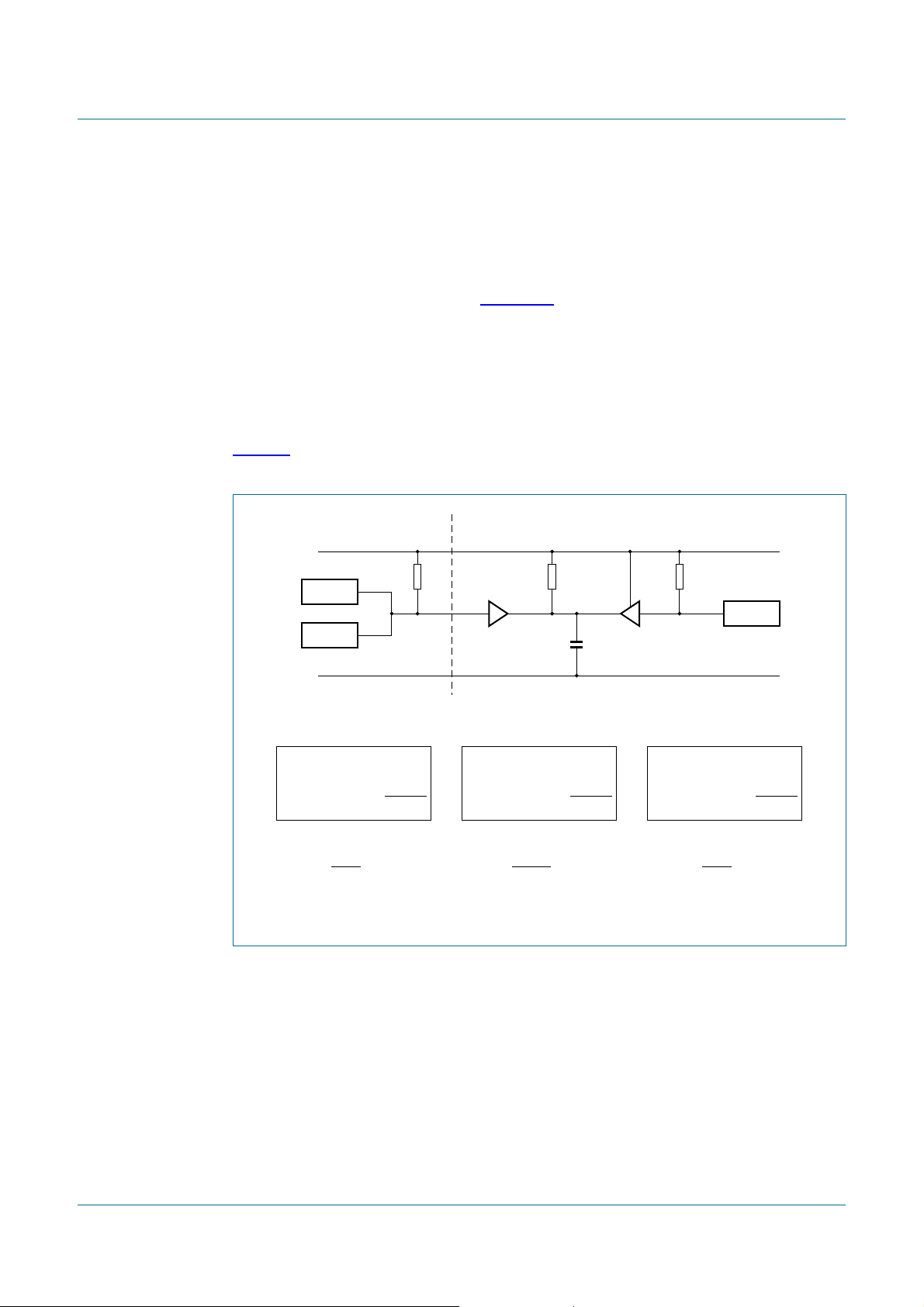
5. Block diagram
P82B715
P82B715
I2C-bus extender
V
CC
Fig 1. Block diagram of P82B715
6. Pinning information
6.1 Pinning
n.c. V
GND n.c.
SDA LDA
SCL
P82B715PN
1
2
Lx Ly
3
Sx Sy
4
002aad686
8
CC
7
6
5
BUFFER
BUFFER
GND
002aad689
P82B715TD
1
n.c. V
2
Lx Ly
3
Sx Sy
4
GND n.c.
002aad687
LCL
8
7
6
5
CC
Fig 2. Pin configuration for DIP8 Fig 3. Pin configuration for SO8
6.2 Pin description
Table 3. Pin description
Symbol Pin Description
n.c. 1 not connected
Lx 2 buffered bus, LDA or LCL
2
Sx 3 I
GND 4 negative supply
n.c. 5 not connected
Sy 6 I
Ly 7 buffered bus, LCL or LDA
V
CC
P82B715_8 © NXP B.V. 2009. All rights reserved.
Product data sheet Rev. 08 — 9 November 2009 3 of 23
8 positive supply
C-bus, SDA or SCL
2
C-bus, SCL or SDA
Page 4

NXP Semiconductors
7. Functional description
The P82B715 is a dual bidirectional logic signal device having unity voltage gain in both
directions, but ×10 current amplification in one direction that allows increasing the
allowableI2C-bus system capacitance. It contains identical circuits for each I2C-bus signal
and requires no external directional control. It uses unidirectional analog current
amplification to increase the current sink capability of I2C-bus chips by a factor of 10 and
to change the I2C-bus specification limit of 400 pF to a 4 nF system limit. This allows
I2C-bus, or similar bus systems, to be extended over long distances using conventional
cables and without degradation of system performance.
P82B715 provides current amplification from its I2C-bus to its low-impedance or buffered
bus. Whenever current is flowing out of Sx, into an I2C-bus chip driving the I2C-bus LOW,
P82B715 will sink ten times that current into Lx to drive the buffered bus LOW (see
Figure 4).
To minimize interference and ensure stability, the current rise and fall times of the Lx drive
amplifier are internally controlled.
The P82B715 does not amplify signal currents flowing in the other direction, i.e., into Sx
from the I2C-bus.The Sx pin is driven LOW by current flowing out of Lx to the driver of that
buffered side.
P82B715
I2C-bus extender
The buffered bus logic LOW voltage at Lx simply drives the I2C-bus at Sx LOW via the
internal 30 Ω resistor. The buffer’s offset voltage (the difference between Sx and Lx)
depends on the current flowing in the sense resistor so it will be very small when the bus
currents are small, but it is guaranteed not to exceed 100 mV in either direction with full
static I2C-bus loading.
The unity voltage gain, with signal current amplification dependent on direction, preserves
the multi-master, bidirectional, open-collector/open-drain, characteristic of any connected
I2C-bus lines and provides these characteristics to the new low-impedance bus. Bus logic
signal voltage levels will be clamped at (VCC+ 0.7 V), but otherwise are independent of
the supply voltage VCC.
= I
I
Sx
Lx
I
Sx
9 × I
I
= 10 × I
Lx
Sx
Sx
Lx buffered bus
002aad688
I2C-bus Sx
V
CC
GND
I
Sx
CURRENT
SENSE
30 Ω
Fig 4. Equivalent circuit: one-half P82B715
7.1 Sx, Sy: I2C-bus SDA or SCL
On the normal side, because the two buffer circuits in the P82B715 are identical, either
the Sx or Sy input pins can be used as the I2C-bus SDA data line, or the SCL clock line.
P82B715_8 © NXP B.V. 2009. All rights reserved.
Product data sheet Rev. 08 — 9 November 2009 4 of 23
Page 5

NXP Semiconductors
7.2 Lx, Ly: buffered bus LDA or LCL
On the special low-impedance or buffered line side, the corresponding output at the Lx or
Ly pins becomes the LDA data line or LCL clock line.
7.3 VCC, GND: positive and negative supply pins
The power supply voltages at each P82B715 used in a system are normally nominally the
same. If they differ by a significant amount, noise margin may be sacrificed as the bus
HIGH level should not exceed the lowest of those supplies.
8. Application design-in information
By using two (or more) P82B715 ICs, a sub-system can be built that retains the interface
characteristics of a normal I2C-bus device so that the sub-system may be included in, or
added onto, any I2C-bus or related system.
The sub-system shown in Figure 5 features a low-impedance or buffered bus, capable of
driving large wiring capacitance.
P82B715
I2C-bus extender
The P82B715 will operate with a supply voltage from 3 V to 12.5 V but the logic signal
levels at Sx/Lx are independent of the chip’s supply. They remain at the levels presented
to the chip by the attached ICs. The maximum static I2C-bus sink current, 3 mA, flowing in
either direction in the internal current sense resistor,causes a difference, or offset voltage,
less than 100 mV between the bus logic LOW levels at Sx and Lx. This makes P82B715
fully compatible with all logic signal drivers, including TTL. The P82B715 cannot modify
the bus logic signal voltage levelsbut it contains internal diodes connected between Lx/Sx
and VCC that will conduct and limit the logic signal swing if the applied logic levels would
have exceeded the supply voltage by more than 0.7 V. In normal applications external
pull-up resistors will pull the connected buses up to the desired voltage HIGH level.
Usually this will be the chip supply, VCC, but for very low logic voltages it is necessary to
use a VCC of at least 3.3 V and preferably even higher. Note that full performance over
temperature is only guaranteed from 4.5 V. Specification de-ratings apply when its supply
voltage is reduced below 4.5 V. The absolute minimum VCC is 3 V.
SDA
SCL
P82B715
1/2
1/2
V
CC
V
CC
long
cable
LDA
LCL
V
V
CC
CC
P82B715
SDA
1/2
I2C-BUS
DEVICE
SCL
1/2
standard
2
C-bus
I
special
buffered bus
special
buffered bus
standard
2
C-bus
I
002aad690
Fig 5. Minimum sub-system with P82B715
P82B715_8 © NXP B.V. 2009. All rights reserved.
Product data sheet Rev. 08 — 9 November 2009 5 of 23
Page 6

NXP Semiconductors
8.1 I2C-bus systems
As in standard I2C-bus systems, pull-up resistors are required to provide the logic HIGH
levels on the buffered bus. (The standard open-collector configuration is retained.) The
value and number of pull-up resistors used is flexible and depends on the system
requirements and designer preferences.
If P82B715 ICs are to be permanently connected into a system it could be configured with
only one pull-up resistor on the buffered bus and none on the I2C-buses, but the system
design will be simplified, and performance improved, by fitting separate pull-ups on each
section of the bus. When a sub-system using P82B715 may be optionally connected to an
existing I2C-bus system that already has a pull-up, then the effects of the sub-system
pull-ups acting in parallel with the existing I2C-bus pull-up must be considered.
8.1.1 Pull-up resistance calculation
When calculating the pull-up resistance values, the gain of the buffer introduces scaling
factors which must be applied to the system components. In practical systems the pull-up
resistance value is usually calculated to achieve the rise time requirement of the system.
As an approximation, this requirement will be satisfied for a standard 100 kHz system if
the time constant of the total system (product of the net resistance and net capacitance) is
set to 1 microsecond or less.
P82B715
I2C-bus extender
In systems using P82B715s, the most convenient way to achieve the total system
rise time requirement is by considering each bus node separately. Each of the I2C-bus
nodes, and the buffered bus node, is designed by selecting its pull-up resistor to provide
the required rise time by setting its time constant (product of the pull-up resistance and
load capacitance) equal to the I2C-bus rise time requirement. If each node complies, then
the system requirement will also be met with a small safety margin.
This arrangement, using multiple pull-ups as in Figure 6, provides the best system
performance and allows stand-alone operation of individual I2C-buses if parts of the
extended system are disconnected or re-connected. For each bus section the pull-up
resistor for a Standard-mode system is calculated as shown in Equation 1:
R
=
-----------------------------------------------------
C device C wiring+
Where: C device = sum of any connected device capacitances, and C wiring = total wiring
and stray capacitance on the bus section.
Remark: The 1 µs is an approximation, with a safety factor, to the theoretical
time-constant necessary to meet the Standard-mode 1 µs bus rise time specification in a
system with variable logic thresholds where the CMOS limits of 30 % and 70 % of V
apply. The actual RC requirement can be shown to be 1.18 µs. For a Fast-mode system,
and the same safety margin, replace the 1 µs with its 300 ns requirement.
If these capacitances cannot be measured or calculated then an approximation can be
made by assuming that each device presents 10 pF of load capacitance and 10 pF of
trace capacitance and that cables range from 50 pF to 100 pF per meter.
1 µs
(1)
CC
If only a single pull-up must be used then it must be placed on the buffered bus (as R2 in
Figure 6) and the associated total system capacitance calculated by combining the
individual bus capacitances into an equivalent capacitive loading on the buffered bus.
P82B715_8 © NXP B.V. 2009. All rights reserved.
Product data sheet Rev. 08 — 9 November 2009 6 of 23
Page 7

NXP Semiconductors
This equivalent capacitance is the sum of the capacitance on the buffered bus plus
10 times the sum of the capacitances on all the connected I2C-bus nodes. The calculated
value should not exceed 4 nF. The single buffered bus pull-up resistor is then calculated to
achievethe rise time requirement and it then provides the pull-up for the buffered bus and
for all other connected I2C-bus nodes included in the calculation.
2
C-bus 1
I
P82B715
I2C-bus extender
V
= 5 V
CC
R3
SDA
I2C-bus 2
SCL
VCC = 5 V
R4
SDA
I2C-bus 3
SCL
SDA
SCL
R1
Sx
Sy
Lx
Ly
R2
buffered bus
Lx
Ly
Lx
Ly
Sx
Sy
Sx
Sy
Fig 6. Single pull-up on buffered bus and multiple pull-up option
8.1.2 Calculating static bus drive currents
Figure 6 shows three P82B715s connected to a common buffered bus. The associated
bus capacitances are omitted for clarity and we assume the pull-up resistors have been
selected to give RC products equal to the bus rise time requirement. An I2C-bus chip
connected at I2C-bus 1 and holding the SDA bus LOW must sink the current flowing in its
local pull-up R1 plus, with assistance from the P82B715, the currents in R2, R3 and R4.
When I2C-bus 1 is LOW, the resistors R3 and R4 act to pull the bus nodes I2C-bus 2 and
I2C-bus 3, and their corresponding Sx pins, to a voltage higher than the voltage at their Lx
pins (which are LOW) so their buffer amplifiers will be inactive.The SDA at Sx of I2C-bus 2
and I2C-bus 3 is pulled LOW by the LOW at Lx via the internal 30 Ω resistor that links Lx
to Sx. So the effective current that must be sunk by the P82B715 bufferon I2C-bus 1, at its
Lx pin, is the sum of the currents in R2, R3 and R4. The Sx current that must be sunk by
an I2C-bus chip at I2C-bus 1, due to the buffer gain action, is1⁄10of the Lx current. So the
effectivepull-up, determining the current to be sunk by an I2C-bus chip at I2C-bus 1, is R1
in parallel with resistors 10 times the values of R2, R3 and R4. If R1 = R3 = R4 = 10 kΩ,
and R2=1kΩ, the effective pull-up load at I2C-bus 1 is
10 kΩ||10 kΩ||100 kΩ||100 kΩ = 4.55 kΩ. (‘||’ means ‘in parallel with’.)
The same calculation applies for I2C-bus 2 or I2C-bus 3.
002aad691
To calculate the current sunk by the Lx pin of the buffer at I2C-bus 1, note that the current
in R1 is sunk directly by the IC at I2C-bus 1. The buffer therefore sinks only the currents
flowing in R2, R3, and R4 so the effective pull-up is R2 in parallel with R3 and R4.
In this example that is 1 kΩ||10 kΩ||10 kΩ = 833 Ω. For a 5.5 V supply and 0.4 V LOW,
that means the buffer is sinking 16.3 mA.
P82B715_8 © NXP B.V. 2009. All rights reserved.
Product data sheet Rev. 08 — 9 November 2009 7 of 23
Page 8
NXP Semiconductors
The P82B715 has a static sink rating of 30 mA at Lx. The requirement is that the pull-up
on the buffered bus, in parallel with all other pull-ups that it is indirectly pulling LOW on Sx
pins of other P82B715 ICs, will not cause this 30 mA limit to be exceeded.
The minimum pull-up resistance in a 5 V ± 10 % system is 170 Ω.
The general requirement is given in Equation 2:
P82B715
I2C-bus extender
V
CC max()
------------------------------------------
0.4 V–
R
PU
30 mA<
Where: RPU= parallel combination of all pull-up resistors driven by the Lx pin of the
P82B715.
Figure 7 shows calculations for an expanded Standard-mode I2C-bus with 3 nF of cable
capacitance.
V
CC
I2C-BUS
I2C-BUS
effective capacitance
2
local bus I
2 × I
total capacitance
C-bus devices
2
C-bus devices
strays
P82B715
SDA
SDA
local bus
20 pF
20 pF
10 pF
50 pF
R1
wiring capacitance
total capacitance
proposed bus expansion
LxSx
LDA
effective capacitance
at common Lx node
3000 pF
3000 pF
R3R2
Lx Sx SDA
3 nF = cable wiring capacitance
effective capacitance
remote I
2
C-bus devices
1 × I
total capacitance
I2C-BUS
2
C-bus devices
strays
P82B715
5 V
0 VGND
10 pF
10 pF
10 pF
30 pF
(2)
2
C-bus pull-up
local I
1 µs
R1 = = 20 kΩ
50 pF
buffered bus pull-up
1 µs
R2 = = 330 Ω
3000 pF
2
C-bus pull-up
remote I
1 µs
R3 = = 33 kΩ
30 pF
002aad692
Fig 7. Typical loading calculation: adding an extension bus with P82B715
P82B715_8 © NXP B.V. 2009. All rights reserved.
Product data sheet Rev. 08 — 9 November 2009 8 of 23
Page 9

NXP Semiconductors
3.3 V
P82B715
I2C-bus extender
R1
BUFFERShMM
C1
R2
LxSx
C2
Lx Sx
1
R3
C3
FRU 1
BUFFER µC
R3
common Lx node
Calculations to ensure rise time is met on each bus section:
effective capacitance
at ShMM buffer
ShMM buffer
P82B715
total capacitance C1
ShMM buffer pull-up
1 µs
R1 = = 25 kΩ
40 pF
strays
10 pF
20 pF
10 pF
40 pF
total capacitance C2
Lx Sx
2
Lx Sx
16
effective capacitance
at common Lx node
17 × P82B715
trace capacitance
Lx common pull-up
R2 = = 5 kΩ
1 µs
200 pF
C3
R3
C3
170 pF
30 pF
200 pF
radial traces
radial trace/connector
total capacitance C3
BUFFER µC
BUFFER µC
effective capacitance
at average radial trace
1 × FRU
P82B715
radial trace pull-up
1 µs
R3 = = 6.2 kΩ
160 pF
Calculation of static loading at ShMM buffer and each FRU:
Loading on ShMM buffer = R1 || {10 (R2 || R3/16)} = 3.5 kΩ
Loading on each FRU = R3 || {10 (R1 || R2 || R3/15)} = 3.76 kΩ
Fig 8. Typical arrangement and calculations for an IPMB analog radial shelf
FRU 2
FRU 16
25 pF
125 pF
10 pF
160 pF
002aad708
Figure 8 shows P82B715 in an analog radial IPMB shelf application.
In this example the total system capacitance is 2800 pF, but it is distributed over 18
different bus sections and no section has a capacitance greater than 200 pF.
If every individual bus section is designed to rise at least as fast as the IPMB requirement,
then when any driver releases the bus, all bus sections will rise together and no amplifiers
in the P82B715s will be activated or, if one is activated, it can only slow the system bus
rise to its own rate and that has been designed to meet the requirement.
It is then only necessary to calculate the equivalent static bus pull-up loading and to
ensure that it exceeds the specification requirement. The calculated loadings meet the
requirements.
Note that in this example only one of the four IPMB lines is shown and the usual switching
arrangements for isolating or cross-connecting bus lines are not shown. The typical offset
(increase in the bus LOW level) measured between any two Sx points in this system is
below 100 mV.
P82B715_8 © NXP B.V. 2009. All rights reserved.
Product data sheet Rev. 08 — 9 November 2009 9 of 23
Page 10

NXP Semiconductors
8.2 Quick design-in point-to-point/multi-point circuit information for 5 V
bus
With many variables (cable length/capacitance, local capacitive loading on each I2C-bus,
bus voltages, and bus speed), optimizing a design can be complex and requires
significant study of the application note information. The following circuit and simplified
approach has been checked to provide adequate performance in the typical 100 kHz
application and can be easily implemented by just using the values and circuit shown for
either point-to-point application, up to 30 meters long, or in multiple point applications if
additional nodes need to be added along the way.
P82B715
I2C-bus extender
5 V
4.7 kΩ 4.7 kΩ
2
I
MASTER
SDA
C-BUS
SCL
µC
Remark: Cable bus pull-ups only fitted at the cable ends, not fitted to modules connected along cable.
Sx
Sy
P82B715
470 Ω 470 Ω
Lx
Ly
5V1
optional
ESD protection
20 meter Cat5e
twisted pair cable
optional
ESD protection
optional
ESD
protection
Fig 9. Quick design-in point-to-point/multi-point circuit for 5 V bus
470 Ω 470 Ω
5V1
Lx
P82B715
Ly
5V1
4.7 kΩ 4.7 kΩ
Lx
P82B715
Ly
4.7 kΩ 4.7 kΩ
Sx
Sy
Sx
Sy
SDA
SCL
SDA
SCL
5 V
I2C-BUS
SLAVE
5 V
I2C-BUS
SLAVE
002aad817
Specific information on this circuit implementation:
• The pull-up on each I
2
C-bus is (VCC− 0.4V)/1mA=4.6kΩ, using 4.7 kΩ as the
nearest usual value.
• The net pull-up on the cable bus can be (V
− 0.5 V) / (21 − n) mA where
CC
n = total number of P82B715 modules on the cable. When there are only two
modules, one each end of the cable, the pull-up = (4.5 / 19) = 237 Ω. Make the
pull-ups at each end of the cable equal. Signalling is bidirectional so there is no
advantage optimizing for any one direction. The pull-up at each end will be 474 Ω,
using 470 Ω as the nearest usual value.
• The 100 kHz rise time requirement is 1 µs. Meeting this requires the product of the
bus capacitance and pull-up resistor on each bus section to be less than 1.18 µs. That
provides one capacitance limit. With 4.7 kΩ pull-ups the I2C-bus limit is 250 pF each,
while the 235 Ω sets a cable bus limit at 5000 pF.
P82B715_8 © NXP B.V. 2009. All rights reserved.
Product data sheet Rev. 08 — 9 November 2009 10 of 23
Page 11

NXP Semiconductors
P82B715
I2C-bus extender
• The 300 ns bus fall time, and the Standard-mode I
2
C-bus limit specification limit of
400 pF, must also be observed. If the 400 pF limit is observed the fall time limit will be
met. Allocate about1⁄3 of this 400 pF limit, or 133 pF, to each I2C-bus leaving2⁄3, or
266 pF, for the cable bus loading as it will appear at the Sx/Sy pins. The ×10 gain of
P82B715 allows the loading at Lx/Ly to be 10 times the load at Sx/Sy, so 2660 pF
maximum. The loading at Lx/Ly due to the other standard buses is 133 pF each. For
just one remote module the cable capacitance may then be up to
(2660 − 133) = 2530 pF. For typical twisted pair or flat cables, as used for telephony or
Ethernet (Cat5e) wiring, that capacitance is around 50 pF to 70 pF / meter so the
cable could, in theory, be up to 50 m long. From practical experience, 30 m has
proven a safe cable length to be driven in this simple way, up to 100 kHz, with the
values shown. Longer distances and higher speeds are possible but require more
careful design.
• If there are severeEMI/ESD tests to be passed then large clamp diodes can be fitted
on the cable bus at each module to VCCand to ground. They may be diodes rated for
this ESD application, or simply large rectifiers (1N4000). The low-impedance bus
easily accommodates their relatively large capacitance. The P82B715 does not
provide any isolation between Lx and Sx, so this clamping method provides the best
protection for the lower voltage I2C-bus parts. The VCC supply should be bypassed
using low-impedance capacitors. Zeners may be fitted to preventthe supply rising due
to rectification during very large interference.
8.3 Comparison of P82B715 versus P82B96 in the quick design-in point-to-point/multi-point circuit
The lower VOL level and ability to operate with any master, slave or bus buffer is the
primary advantage of the using the P82B715 for long distance buses at the disadvantage
of not isolating bus capacitance like the P82B96 or PCA9600 are able to do. The primary
disadvantage of the P82B96 and PCA9600 is that the static level offset needed to isolate
bus capacitance does not allow these devices to operate with other bus buffers with
special offset levels or with master/slaves that require a VIL lower than 0.8 V with noise
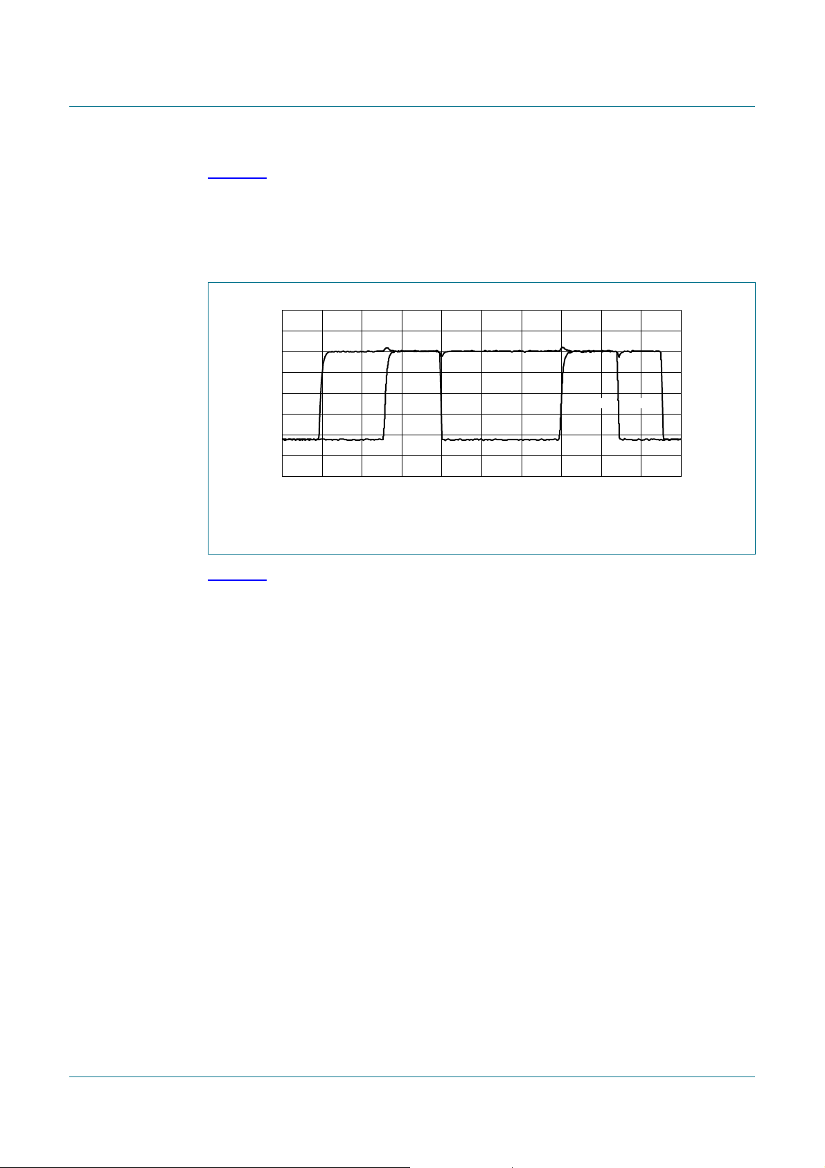
margin. Waveforms using the circuit shown in Figure 9 are shown in Figure 10 using the
P82B715 and Figure 11 using the P82B96 so that the designer can clearly see these
trade-offs and choose the type of device that is best for their application.
7
voltage
(V)
5
3
1
−1
0 20168124
SDA
SDA
SCL
SCL
002aad818
SDA
SCL
time (µs)
Fig 10. Clock and data signal output at Sx/Sy from a system with P82B715 at each end of
a 20 m cable
P82B715_8 © NXP B.V. 2009. All rights reserved.
Product data sheet Rev. 08 — 9 November 2009 11 of 23
Page 12
NXP Semiconductors
Figure 10 shows the I2C-bus waveforms from the long distance line as seen by the slave
on the P82B715 Sx/Sy I/O. Notice that the offset is small and the static levels remain
under 0.4 V. Coupling of SDA to SCL is negligible when SCL is LOW but slight
cross-coupling of SCL to SDA is visible when SDA is HIGH and therefore higher
impedance. The waveforms are very clean and will easily support all available I2C-bus
masters and slaves.
P82B715
I2C-bus extender
7
voltage
(V)
5
3
1
−1
0 20168124
SDA
SCL
SCL
SDA
SCL
SCL
002aad819
SDA
time (µs)
Fig 11. Clock and data signal output to a slave from Sx/Sy of a P82B96 replacing one of
the P82B715s
Figure 11 shows the waveforms on the Sx/Sy I/O as seen by the slave when a P82B96 is
substituted. P82B96 uses a static level offset on the slave side to isolate noise and
loadings on either side of this device. The nominal offset is 0.8 V and that VOLmay create
worst-case design tolerance problems with slave devices that do not use I2C-bus
switching levels, for example TTL levels. It also precludes operation with other bus buffers
using special non-compliant I2C-bus levels.
The P82B96 does not actually interfere with the operation of compliant I2C-bus devices
down to at least 2.7 V supply or even with TTL devices (that switch around 1.4 V). It only
causes a theoretical worst case design tolerance problem because TTL devices have a
worst case 0.8 V requirement. A TTL designer must center the actual switch point
between the two specified limits, 0.8 V and 2.1 V, so in reality it cannot ever approach the
problem 0.8 V theoretical limit.
The PCA9600 is an improved version of the P82B96 offering 1 MHz operation and lower,
more closely controlled VOL on the Sx and Sy pins.
P82B715_8 © NXP B.V. 2009. All rights reserved.
Product data sheet Rev. 08 — 9 November 2009 12 of 23
Page 13

NXP Semiconductors
9. Limiting values
Table 4. Limiting values
In accordance with the Absolute Maximum Rating System (IEC 60134).
Symbol Parameter Conditions Min Max Unit
V
CC
V
bus
V
buff
I DC current (any pin) - 60 mA
P
tot
T
stg
T
amb
[1] Voltages with respect to GND.
The bus voltages quoted are DC voltages and are allowed to be exceeded during any negative transient
undershoot that may be generated by normal operation of P82B715, P82B96 or PCA9600 when any of
those parts are driving long PCB traces, wiring or cables. The Lx/Sx pins have internal protective diodes to
GND that will conduct when the applied bus voltage exceeds approximately −0.6 V and these diodes will
limit the amplitude of the negative undershoot. If required, fitting additional Schottky diodes such as
BAT54A at Sx/Sy may be used to further ensure any undershoot at these pins does not cause conduction of
the diodes inside other ICs connected to Sx/Sy.
P82B715
I2C-bus extender
supply voltage
voltage range I2C-bus, SCL or SDA
voltage range buffered bus
total power dissipation - 300 mW
storage temperature −55 +125 °C
ambient temperature operating −40 +85 °C
[1]
−0.3 +12 V
[1]
0VCCV
[1]
0VCCV
10. Characteristics
Table 5. Characteristics
T
=25°C; VCC= 5 V; unless otherwise specified.
amb
Symbol Parameter Conditions Min Typ Max Unit
Power supply
V
CC
I
CC
supply voltage operating
supply current - 14 - mA
Drive currents
, I
I
Sx
Sy
I
, I
Lx
Ly
output sink on I2C-bus VCC>3V; VSx,VSyLOW = 0.4 V;
output sink on buffered bus VLx, VLy LOW = 0.4 V;
Derated dynamic drive currents for V
ILx, I
Ly
output sink on buffered bus VCC>3V;
=12V - 15 - mA
V
CC
2
C-bus inputs LOW; both
both I
buffered outputs sinking 30 mA
CC
V
I
Lx
V
< 4.5 V
V
I
Sx,ISy
V
V
I
Sx,ISy
LOW on buffered bus = 0.3 V;
Lx,VLy
, ILy= −3mA
LOW on I2C-bus = 0.3 V
Sx,VSy
[1]
LOW = 0.4 V to 1.5 V;
Lx,VLy
sinking on I2C-bus < −4mA
>3V;
CC
LOW = 1.5 V to VCC;
Lx,VLy
sinking on I2C-bus = −7mA
[1]
4.5 - 12 V
-22-mA
[2]
3- - mA
30 - - mA
24 - - mA
24 - - mA
P82B715_8 © NXP B.V. 2009. All rights reserved.
Product data sheet Rev. 08 — 9 November 2009 13 of 23
Page 14

NXP Semiconductors
P82B715
I2C-bus extender
Table 5. Characteristics
T
=25°C; VCC= 5 V; unless otherwise specified.
amb
…continued
Symbol Parameter Conditions Min Typ Max Unit
Input currents
, I
I
Sx
Sy
, I
I
Lx
Ly
, I
I
Lx
Ly
input current from I2C-bus ILx, ILy sink on buffered bus = 30mA - - −3mA
input current from buffered bus VCC>3V; ISx, ISy sink on
2
I
C-bus = 3 mA
leakage current on buffered bus VCC= 3 V to 12 V; VLx, VLy=VCC and
V
, VSy=V
Sx
CC
[2]
--−3mA
- - 200 µA
Impedance transformation
Z
in/Zout
input/output impedance VSx<VLx and the buffer is active;
I
sinking 30 mA on buffered bus
Lx
81013
Buffer delay times
t
rise/fall delay
ISxto V
ISyto V
t
rise/fall delay
VLxto V
VLyto V
[1] Operation with reduced performance is possible down to 3 V.Typical static sinking performance is not degraded at 3 V, but the dynamic
sink currents while the output is being driven through 0.5VCC are reduced and can increase fall times. Timing-critical designs should
accommodate the guaranteed minimums.
[2] Buffer is passive in this test. The Sx/Sy sink current flows via an internal resistor to the driver connected at the Lx/Ly I/O.
[3] A conventional input-output delay will not be observed in the Sx/Lx voltage waveforms because the input and output pins are internally
tied with a 30 Ω resistor so they show equal logic voltage levels, to within 100 mV. When connected in an I2C-bus system, an Sx/Sy
input pin cannot rise/fall until the buffered busload at the output pin has been driven by the internal amplifier. This test measures the bus
propagation delay caused to falling or rising voltages at the Lx/Ly output (as well as the Sx/Sy input) by the amplifier’s response time.
The figure given is measured with a drive current as shown in Figure 12. Because this is a dynamic bus test in which a corresponding
bus driving IC has an output voltage well above 0.4V, 6 mA is used instead of the static 3 mA.
[4] The signal path Lx to Sx and Ly to Sy is passive via the internal 30 Ω resistor. There is no amplifier involved and essentially no signal
propagation delay.
time delay to VLx voltage
crossing 0.5V
Lx
current step I
Ly
for input drive
CC
at Sx
Sx
buffer time delay of switching
edges between V
Sx
V
Sy
output
Sx
input and
Lx
Figure 12; RLx pull-up = 270 Ω;
see
no capacitive load; V
pull-up = 4700 Ω;
R
Sx
no capacitive load; V
CC
CC
=5V
=5V
[3]
- 250 - ns
[4]
-0-ns
11. Test information
5 V
input
current
input and
voltage
output
t
delay
t
delay
5 V
0 V
002aad693
input
I = 6 mA
4.7 kΩ
Sx Lx
P82B715
V V V
270 Ω
Lx Sx
P82B715
4.7 kΩ
output
Fig 12. Test circuit for delay times
P82B715_8 © NXP B.V. 2009. All rights reserved.
Product data sheet Rev. 08 — 9 November 2009 14 of 23
Page 15

NXP Semiconductors
12. Package outline
P82B715
I2C-bus extender
DIP8: plastic dual in-line package; 8 leads (300 mil)
D
seating plane
A
L
Z
e
b
8
pin 1 index
1
w M
b
1
b
2
5
SOT97-1
M
E
A
2
A
c
(e )
1
M
H
E
1
DIMENSIONS (inch dimensions are derived from the original mm dimensions)
A
UNIT
mm
inches
Note
1. Plastic or metal protrusions of 0.25 mm (0.01 inch) maximum per side are not included.
A
max.
OUTLINE
VERSION
SOT97-1
A
12
min.
max.
050G01 MO-001 SC-504-8
b
1.73
0.53
1.14
0.38
0.068
0.021
0.045
0.015
IEC JEDEC JEITA
b
1
4
0 5 10 mm
scale
b
2
0.36
1.07
0.23
0.89
0.014
0.042
0.009
0.035
REFERENCES
(1) (1)
cD E e M
9.8
6.48
9.2
6.20
0.39
0.26
0.36
0.24
1
3.60
3.05
0.14
0.12
E
8.25
7.80
0.32
0.31
EUROPEAN
PROJECTION
10.0
0.39
0.33
M
L
e
H
8.3
w
max.
0.2542.54 7.62
1.154.2 0.51 3.2
0.010.1 0.3
0.0450.17 0.02 0.13
ISSUE DATE
99-12-27
03-02-13
(1)
Z
Fig 13. Package outline SOT97-1 (DIP8)
P82B715_8 © NXP B.V. 2009. All rights reserved.
Product data sheet Rev. 08 — 9 November 2009 15 of 23
Page 16

NXP Semiconductors
P82B715
I2C-bus extender
SO8: plastic small outline package; 8 leads; body width 3.9 mm
D
c
y
Z
8
pin 1 index
1
e
5
A
2
A
4
w M
b
p
SOT96-1
E
H
E
1
detail X
A
X
v M
A
Q
(A )
L
p
L
A
3
θ
0 2.5 5 mm
scale
DIMENSIONS (inch dimensions are derived from the original mm dimensions)
mm
OUTLINE
VERSION
SOT96-1
A
A1A2A3b
max.
0.25
1.75
0.10
0.010
0.069
0.004
p
1.45
1.25
0.057
0.049
IEC JEDEC JEITA
076E03 MS-012
0.25
0.01
0.49
0.36
0.019
0.014
0.25
0.19
0.0100
0.0075
UNIT
inches
Notes
1. Plastic or metal protrusions of 0.15 mm (0.006 inch) maximum per side are not included.
2. Plastic or metal protrusions of 0.25 mm (0.01 inch) maximum per side are not included.
(1)E(2)
cD
5.0
4.8
0.20
0.19
REFERENCES
eHELLpQZywv θ
4.0
3.8
0.16
0.15
1.27
0.05
6.2
5.8
0.244
0.228
1.05
1.0
0.4
0.039
0.016
0.7
0.6
0.028
0.024
0.25 0.10.25
0.010.010.041 0.004
EUROPEAN
PROJECTION
(1)
0.7
0.3
0.028
0.012
ISSUE DATE
99-12-27
03-02-18
o
8
o
0
Fig 14. Package outline SOT96-1 (SO8)
P82B715_8 © NXP B.V. 2009. All rights reserved.
Product data sheet Rev. 08 — 9 November 2009 16 of 23
Page 17

NXP Semiconductors
13. Soldering of SMD packages
This text provides a very brief insight into a complex technology. A more in-depth account
of soldering ICs can be found in Application Note
soldering description”
13.1 Introduction to soldering
Soldering is one of the most common methods through which packages are attached to
Printed Circuit Boards (PCBs), to form electrical circuits. The soldered joint provides both
the mechanical and the electrical connection. There is no single soldering method that is
ideal for all IC packages. Wave soldering is often preferred when through-hole and
Surface Mount Devices (SMDs) are mixed on one printed wiring board; however, it is not
suitable for fine pitch SMDs. Reflow soldering is ideal for the small pitches and high
densities that come with increased miniaturization.
13.2 Wave and reflow soldering
Wave soldering is a joining technology in which the joints are made by solder coming from
a standing wave of liquid solder. The wave soldering process is suitable for the following:
.
P82B715
I2C-bus extender
AN10365 “Surface mount reflow
• Through-hole components
• Leaded or leadless SMDs, which are glued to the surface of the printed circuit board
Not all SMDs can be wave soldered. Packages with solder balls, and some leadless
packages which have solder lands underneath the body, cannot be wave soldered. Also,
leaded SMDs with leads having a pitch smaller than ~0.6 mm cannot be wave soldered,
due to an increased probability of bridging.
The reflow soldering process involves applying solder paste to a board, followed by
component placement and exposure to a temperature profile. Leaded packages,
packages with solder balls, and leadless packages are all reflow solderable.
Key characteristics in both wave and reflow soldering are:
• Board specifications, including the board finish, solder masks and vias
• Package footprints, including solder thieves and orientation
• The moisture sensitivity level of the packages
• Package placement
• Inspection and repair
• Lead-free soldering versus SnPb soldering
13.3 Wave soldering
Key characteristics in wave soldering are:
• Process issues, such as application of adhesive and flux, clinching of leads, board
transport, the solder wave parameters, and the time during which components are
exposed to the wave
• Solder bath specifications, including temperature and impurities
P82B715_8 © NXP B.V. 2009. All rights reserved.
Product data sheet Rev. 08 — 9 November 2009 17 of 23
Page 18

NXP Semiconductors
13.4 Reflow soldering
Key characteristics in reflow soldering are:
• Lead-freeversusSnPb soldering; note that a lead-free reflow process usually leads to
• Solder paste printing issues including smearing, release, and adjusting the process
• Reflow temperature profile; this profile includes preheat, reflow (in which the board is
Table 6. SnPb eutectic process (from J-STD-020C)
Package thickness (mm) Package reflow temperature (°C)
< 2.5 235 220
≥ 2.5 220 220
P82B715
I2C-bus extender
higher minimum peak temperatures (see Figure 15) than a SnPb process, thus
reducing the process window
window for a mix of large and small components on one board
heated to the peak temperature) and cooling down. It is imperative that the peak
temperature is high enough for the solder to make reliable solder joints (a solder paste
characteristic). In addition, the peak temperature must be low enough that the
packages and/or boards are not damaged. The peak temperature of the package
depends on package thickness and volume and is classified in accordance with
Table 6 and 7
Volume (mm3)
< 350 ≥ 350
Table 7. Lead-free process (from J-STD-020C)
Package thickness (mm) Package reflow temperature (°C)
Volume (mm3)
< 350 350 to 2000 > 2000
< 1.6 260 260 260
1.6 to 2.5 260 250 245
> 2.5 250 245 245
Moisture sensitivity precautions, as indicated on the packing, must be respected at all
times.
Studies have shown that small packages reach higher temperatures during reflow
soldering, see Figure 15.
P82B715_8 © NXP B.V. 2009. All rights reserved.
Product data sheet Rev. 08 — 9 November 2009 18 of 23
Page 19

NXP Semiconductors
Fig 15. Temperature profiles for large and small components
maximum peak temperature
temperature
MSL: Moisture Sensitivity Level
= MSL limit, damage level
minimum peak temperature
= minimum soldering temperature
P82B715
I2C-bus extender
peak
temperature
time
001aac844
For further information on temperature profiles, refer to Application Note
“Surface mount reflow soldering description”
.
14. Soldering of through-hole mount packages
14.1 Introduction to soldering through-hole mount packages
This text gives a very brief insight into wave, dip and manual soldering.
Wave soldering is the preferred method for mounting of through-hole mount IC packages
on a printed-circuit board.
14.2 Soldering by dipping or by solder wave
Driven by legislation and environmental forces the worldwide use of lead-free solder
pastes is increasing. Typical dwell time of the leads in the wave ranges from
3 seconds to 4 seconds at 250 °C or 265 °C, depending on solder material applied, SnPb
or Pb-free respectively.
The total contact time of successive solder waves must not exceed 5 seconds.
The device may be mounted up to the seating plane, but the temperature of the plastic
body must not exceed the specified maximum storage temperature (T
printed-circuit board has been pre-heated, forced cooling may be necessary immediately
after soldering to keep the temperature within the permissible limit.
AN10365
stg(max)
). If the
14.3 Manual soldering
Apply the soldering iron (24 V or less) to the lead(s) of the package, either below the
seating plane or not more than 2 mm aboveit. If the temperature of the soldering iron bit is
less than 300 °C it may remain in contact for up to 10 seconds. If the bit temperature is
between 300 °C and 400 °C, contact may be up to 5 seconds.
P82B715_8 © NXP B.V. 2009. All rights reserved.
Product data sheet Rev. 08 — 9 November 2009 19 of 23
Page 20

NXP Semiconductors
14.4 Package related soldering information
Table 8. Suitability of through-hole mount IC packages for dipping and wave soldering
Package Soldering method
CPGA, HCPGA - suitable
DBS, DIP, HDIP, RDBS, SDIP, SIL suitable suitable
PMFP
[1] For SDIP packages, the longitudinal axis must be parallel to the transport direction of the printed-circuit
[2] For PMFP packages hot bar soldering or manual soldering is suitable.
15. Abbreviations
Table 9. Abbreviations
Acronym Description
AdvancedTCA Advanced Telecom Computing Architecture
CMOS Complementary Metal-Oxide Semiconductor
DDC Data Display Channel
EMI ElectroMagnetic Interference
ESD ElectroStatic Discharge
FRU Field Replaceable Unit
HBM Human Body Model
2
C-bus Inter-Integrated Circuit bus
I
I/O Input/Output
IC Integrated Circuit
IPMB Intelligent Platform Management Bus
MM Machine Model
PMBus Power Management Bus
RC Resistor-Capacitor network
ShMM Shelf Management Module
SMBus System Management Bus
TTL Transistor-Transistor Logic
[2]
board.
P82B715
I2C-bus extender
Dipping Wave
[1]
- not suitable
P82B715_8 © NXP B.V. 2009. All rights reserved.
Product data sheet Rev. 08 — 9 November 2009 20 of 23
Page 21

NXP Semiconductors
P82B715
I2C-bus extender
16. Revision history
Table 10. Revision history
Document ID Release date Data sheet status Change notice Supersedes
P82B715_8 20091109 Product data sheet - P82B715_7
Modifications:
P82B715_7 20080529 Product data sheet - P82B715_6
P82B715_6
(9397 750 12452)
P82B715_5
(9397 750 11094)
P82B715_4
(9397 750 08163)
• Table 4 “Limiting values”, Table note [1]: added 2
20031202 Product data ECN 853-2240 01-A14516
20030220 Product data ECN 853-2240 29410
20010306 Product data ECN 853-2240 25757
nd
paragraph.
of 14 Nov 2003
of 22 Jan 2003
of 06 Mar 2001
P82B715_5
P82B715_4
P82B715_3
P82B715_8 © NXP B.V. 2009. All rights reserved.
Product data sheet Rev. 08 — 9 November 2009 21 of 23
Page 22

NXP Semiconductors
17. Legal information
17.1 Data sheet status
P82B715
I2C-bus extender
Document status
Objective [short] data sheet Development This document contains data from the objective specification for product development.
Preliminary [short] data sheet Qualification This document contains data from the preliminary specification.
Product [short] data sheet Production This document contains the product specification.
[1] Please consult the most recently issued document before initiating or completing a design.
[2] The term ‘short data sheet’ is explained in section “Definitions”.
[3] The product statusof device(s) described inthis document mayhave changed sincethis document waspublished and maydiffer incase of multipledevices. The latestproduct status
information is available on the Internet at URL
[1][2]
Product status
17.2 Definitions
Draft — The document is a draft version only. The content is still under
internal review and subject to formal approval, which may result in
modifications or additions. NXP Semiconductors does not give any
representations or warranties as to the accuracy or completeness of
information includedhereinand shall havenoliability for theconsequencesof
use of such information.
Short data sheet — A short data sheet is an extract from a full data sheet
with thesameproduct type number(s) andtitle. A short data sheet isintended
for quickreference only and should not be relied upontocontain detailed and
full information. For detailed and full information see the relevant full data
sheet, which is available on request via the local NXP Semiconductors sales
office. In case of any inconsistency or conflict with the short data sheet, the
full data sheet shall prevail.
17.3 Disclaimers
General — Information in this document is believed to be accurate and
reliable. However,NXP Semiconductors does not give anyrepresentationsor
warranties, expressedor implied, as to the accuracyorcompleteness of such
information and shall have no liability for the consequences of use of such
information.
Right to make changes — NXP Semiconductors reserves the right to make
changes to information published in this document, including without
limitation specifications and product descriptions, at any time and without
notice. This documentsupersedesandreplaces all information supplied prior
to the publication hereof.
Suitability for use — NXP Semiconductors products are not designed,
authorized or warranted to be suitable for use in medical, military, aircraft,
space or life support equipment, nor in applications where failure or
malfunction of an NXP Semiconductors product can reasonably be expected
to result in personal injury, death or severe property or environmental
[3]
http://www.nxp.com.
Definition
damage. NXP Semiconductors accepts no liability for inclusion and/or use of
NXP Semiconductors products in such equipment or applications and
therefore such inclusion and/or use is at the customer’s own risk.
Applications — Applications that are described herein for any of these
products are for illustrative purposes only. NXP Semiconductors makes no
representation or warranty that such applications will be suitable for the
specified use without further testing or modification.
Limiting values — Stress above one or more limiting values (as defined in
the Absolute MaximumRatingsSystem of IEC 60134) may cause permanent
damage to thedevice. Limitingvalues are stressratingsonly and operation of
the device at these or any other conditions above those given in the
Characteristics sections of this document is not implied. Exposure to limiting
values for extended periods may affect device reliability.
Terms and conditions of sale — NXP Semiconductors products are sold
subject to the general terms and conditions of commercial sale, as published
at
http://www.nxp.com/profile/terms, including those pertaining to warranty,
intellectual property rights infringement and limitation of liability, unless
explicitly otherwise agreed to in writing by NXP Semiconductors. In case of
any inconsistency or conflict between information in this document and such
terms and conditions, the latter will prevail.
No offer to sell or license — Nothing in this document may be interpreted
or construed as an offer to sell products that is open for acceptance or the
grant, conveyance or implication of anylicenseunder any copyrights, patents
or other industrial or intellectual property rights.
Export control — This document as well as the item(s) described herein
may be subject to export control regulations. Export might require a prior
authorization from national authorities.
17.4 Trademarks
Notice: Allreferenced brands, productnames, service names and trademarks
are the property of their respective owners.
I2C-bus — logo is a trademark of NXP B.V.
18. Contact information
For more information, please visit: http://www.nxp.com
For sales office addresses, please send an email to: salesaddresses@nxp.com
P82B715_8 © NXP B.V. 2009. All rights reserved.
Product data sheet Rev. 08 — 9 November 2009 22 of 23
Page 23

NXP Semiconductors
19. Contents
P82B715
I2C-bus extender
1 General description . . . . . . . . . . . . . . . . . . . . . . 1
2 Features . . . . . . . . . . . . . . . . . . . . . . . . . . . . . . . 1
3 Applications . . . . . . . . . . . . . . . . . . . . . . . . . . . . 2
4 Ordering information. . . . . . . . . . . . . . . . . . . . . 2
4.1 Ordering options. . . . . . . . . . . . . . . . . . . . . . . . 2
5 Block diagram . . . . . . . . . . . . . . . . . . . . . . . . . . 3
6 Pinning information. . . . . . . . . . . . . . . . . . . . . . 3
6.1 Pinning . . . . . . . . . . . . . . . . . . . . . . . . . . . . . . . 3
6.2 Pin description . . . . . . . . . . . . . . . . . . . . . . . . . 3
7 Functional description . . . . . . . . . . . . . . . . . . . 4
7.1 Sx, Sy: I
2
C-bus SDA or SCL. . . . . . . . . . . . . . . 4
7.2 Lx, Ly: buffered bus LDA or LCL. . . . . . . . . . . . 5
7.3 V
, GND: positive and negative supply pins. . 5
CC
8 Application design-in information . . . . . . . . . . 5
8.1 I
2
C-bus systems . . . . . . . . . . . . . . . . . . . . . . . . 6
8.1.1 Pull-up resistance calculation. . . . . . . . . . . . . . 6
8.1.2 Calculating static bus drive currents. . . . . . . . . 7
8.2 Quick design-in point-to-point/multi-point
circuit information for 5 V bus . . . . . . . . . . . . . 10
8.3 Comparison of P82B715 versus P82B96
in the quick design-in point-to-point/
multi-point circuit. . . . . . . . . . . . . . . . . . . . . . . 11
9 Limiting values. . . . . . . . . . . . . . . . . . . . . . . . . 13
10 Characteristics. . . . . . . . . . . . . . . . . . . . . . . . . 13
11 Test information. . . . . . . . . . . . . . . . . . . . . . . . 14
12 Package outline . . . . . . . . . . . . . . . . . . . . . . . . 15
13 Soldering of SMD packages . . . . . . . . . . . . . . 17
13.1 Introduction to soldering . . . . . . . . . . . . . . . . . 17
13.2 Wave and reflow soldering . . . . . . . . . . . . . . . 17
13.3 Wave soldering. . . . . . . . . . . . . . . . . . . . . . . . 17
13.4 Reflow soldering . . . . . . . . . . . . . . . . . . . . . . . 18
14 Soldering of through-hole mount packages . 19
14.1 Introduction to soldering through-hole mount
packages . . . . . . . . . . . . . . . . . . . . . . . . . . . . 19
14.2 Soldering by dipping or by solder wave . . . . . 19
14.3 Manual soldering . . . . . . . . . . . . . . . . . . . . . . 19
14.4 Package related soldering information . . . . . . 20
15 Abbreviations. . . . . . . . . . . . . . . . . . . . . . . . . . 20
16 Revision history. . . . . . . . . . . . . . . . . . . . . . . . 21
17 Legal information. . . . . . . . . . . . . . . . . . . . . . . 22
17.1 Data sheet status . . . . . . . . . . . . . . . . . . . . . . 22
17.2 Definitions. . . . . . . . . . . . . . . . . . . . . . . . . . . . 22
17.3 Disclaimers . . . . . . . . . . . . . . . . . . . . . . . . . . . 22
17.4 Trademarks. . . . . . . . . . . . . . . . . . . . . . . . . . . 22
18 Contact information . . . . . . . . . . . . . . . . . . . . 22
19 Contents. . . . . . . . . . . . . . . . . . . . . . . . . . . . . . 23
Please be aware that important notices concerning this document and the product(s)
described herein, have been included in section ‘Legal information’.
© NXP B.V. 2009. All rights reserved.
For more information, please visit: http://www.nxp.com
For sales office addresses, please send an email to: salesaddresses@nxp.com
Date of release: 9 November 2009
Document identifier: P82B715_8
 Loading...