

Page 1

NXP Semiconductors
IMXRT500EC
Data Sheet: Technical Data Rev. 0, 02/2021
i.MX RT500 Low-Power
Crossover Processor
The i.MX RT500 is a family of dual-core microcontrollers for
embedded applications featuring an Arm Cortex-M33 CPU
combined with a Cadence® Xtensa® Fusion F1 Audio Digital
Signal Processor CPU. The Cortex-M33 includes two hardware
coprocessors providing enhanced performance for an array of
complex algorithms along with a 2D Vector GPU with LCD
Interface and MIPI DSI PHY. The family offers a rich set of
peripherals and very low power consumption. The device has up
to 5 MB SRAM, two FlexSPIs (Octal/Quad SPI Interfaces) each
with 32 KB cache, one with dynamic decryption, high-speed USB
device/host + PHY, 12-bit 1 MS/s ADC, Analog Comparator,
Audio subsystems supporting up to 8 DMIC channels, 2D GPU
and LCD Controller with MIPI DSI PHY, SDIO/eMMC; FlexIO;
AES/SHA/Crypto M33 coprocessor and PUF key generation
Control processor core
• Arm Cortex-M33 processor, running at frequencies of
up to 200 MHz
• Arm TrustZone
• Arm Cortex-M33 built-in Memory Protection Unit (MPU)
supporting eight regions
• Single-precision Hardware Floating Point Unit (FPU).
• Arm Cortex-M33 built-in Nested Vectored Interrupt
Controller (NVIC).
• Non-maskable Interrupt (NMI) input.
• Two coprocessors for the Cortex-M33: a hardware
accelerator for fixed and floating point DSP functions
(PowerQuad) and a Crypto/FFT engine (Casper). The
DSP coprocessor uses a bank of four dedicated 2 KB
SRAMs. The Crypto/FFT engine uses a bank of two 2
KB SRAMs that are also AHB accessible by the CPU
and the DMA engine.
• Serial Wire Debug with eight break points, four watch
points, and a debug timestamp counter. It includes
Serial Wire Output (SWO) trace and ETM trace.
• Cortex-M33 System tick timer
DSP processor core
• Cadence Tensilica Fusion F1 DSP processor, running
at frequencies of up to 200 MHz.
• Hardware Floating Point Unit.
• Serial Wire Debug (shared with Cortex-M33 Control
Domain CPU).
Communication interface
• 9 configurable universal serial interface modules
(Flexcomm Interfaces). Each module contains an
integrated FIFO and DMA support. Each of the nine
modules can be configured as:
• Two additional high-speed SPI interfaces supporting
50 MHz operation
• One additional I2C interface with open-drain pads
• Two I3C bus interfaces
• A digital microphone interface supporting up to 8
channels with associated decimators and Voice
MIMXRT5XXSFFOC
MIMXRT5XXSFFOCR
MIMXRT5XXSFAWCR
249 FOWLP 7.0mm x
7.0mm x 0.725mm,
0.4mm pitch
• A USART with dedicated fractional baud rate
generation and flow-control handshaking
signals. The USART can optionally be clocked
at 32 kHz and operated when the chip is in
reduced power mode, using either the 32 kHz
clock or an externally supplied clock. The
USART also provides partial support for
LIN2.2.
• An I2C-bus interface with multiple address
recognition, and a monitor mode. It supports
400 Kb/sec Fast-mode and 1 Mb/sec Fastmode Plus. It also supports 3.4 Mb/sec highspeed when operating in slave mode.
• An SPI interface.
• An I2S (Inter-IC Sound) interface for digital
audio input or output. Each I2S supports up to
four channel-pairs.
141 WLCSP 4.525mm
x 4.525mm x 0.49mm,
0.35mm pitch
NXP reserves the right to change the production detail specifications as may be
required to permit improvements in the design of its products.
Page 2

Five I/O Power Rails
• Five independent supplies powering different clusters
of pins to permit interfacing directly to off-chip
peripherals operating at different supply levels.
On-chip memory
• Up to 5 MB of system SRAM accessible by both CPUs,
both DMA engines, the Graphics Subsystem and all
other AHB masters.
• Additional SRAMs for USB traffic (16 KB), Cortex-M33
co-processors (4 x 2 KB), SDIO FIFOs (2 x 512 B dualport), PUF secure key generation (2 KB), FlexSPI
caches (32 KB each), SmartDMA commands (32 KB),
and a variety of dual and single port RAMs for
graphics.
• 16 kbits OTP fuses
• Up to 192 KB ROM memory for factory-programmed
drivers and APIs
• System boot from High-speed SPI, FlexSPI Flash, HS
USB, I2C, UART or eMMC via on-chip bootloader
software included in ROM. FlexSPI boot mode will
include an option for Execute-in-place start-up for nonsecure boot.
Digital peripherals
• Two general purpose DMA engines, each with 37
channels and up to 27 programmable request/trigger
sources.
• Can be configured such that one DMA is secure
and the other non-secure and/or one can be
designated for use by the M33 CPU and the
other by the DSP
• Smart DMA Controller with dedicated 32KB code RAM
• USB high-speed host/device controller with on-chip
PHY and dedicated DMA controller.
• Two FlexSPI (Octal/Quad) Interfaces up to 200 MHz
DDR/SDR (target). 32 KB caches with selectable
cache policies based on programmable address
regions. One of the FlexSPI interface will include onthe-fly decryption for execute-in-place and addressremapping to support dual-image boot. DMA supported
(both modules).
• Two SD/eMMC memory card interfaces with dedicated
DMA controllers. One supports eMMC 5.0 with
HS400/DDR operation.
Analog peripherals
• One 12-bit ADC with sampling rates of 1 Msamples/sec
and an enhanced ADC controller. It supports up to 10
single-ended channels or 5 differential channels. The
ADC supports DMA.
• Temperature sensor.
• Analog comparator
Activation Detect. One pair of channels can be
streamed directly to I2S. The DMIC supports DMA.
Timers
• One 32-bit SCTimer/PWM module (SCT). Multipurpose timer with extensive event-generation,
match/compare, and complex PWM and output
control features.
• 10 general-purpose/PWM outputs, 8 generalpurpose inputs
• It supports DMA and can trigger external DMA
events
• It supports fractional match values for high
resolution
• Five general purpose, 32-bit timer/counter modules
with PWM capability
• 24-bit multi-rate timer module with 4 channels each
capable of generating repetitive interrupts at
different, programmable frequencies.
• Two Windowed Watchdog Timers (WDT) with
dedicated watchdog oscillator (1 MHz LPOSC)
• Frequency measurement module to determine the
frequency of a selection of on-chip or off-chip clock
sources.
• Real-Time Clock (RTC) with independent power
supply and dedicated oscillator. Integrated wake-up
timer can be used to wake the device up from lowpower modes. The RTC resides in the “always-on”
voltage domain. RTC includes eight 32-bit generalpurpose registers which can retain contents when
power is removed from the rest of the chip.
• Ultra-low power micro-tick Timer running from the
Watchdog oscillator with capture capability for
timestamping. Can be used to wake up the device
from low-power modes.
• 64-bit OS/Event Timer common to both processors
with individual match/capture and interrupt
generation logic. Enabled on POR
Clocks
• Crystal oscillator with an operating range of 4 MHz
to 26 MHz.
• Dual trim option: Internal 192/96 MHz FRO
oscillator. Trimmed to 1% accuracy.
• FRO capable of being tuned using an accurate
reference clock (eg. XTAL Osc) to 0.1% accuracy
with 46% duty cycle to support MIPI PHY and
FlexSPI.
• Internal 1 MHz low-power oscillator with 5%
accuracy. Serves as the watchdog oscillator and
clock for the OS/Event Timer and the Systick among
others. Also available as the system clock to both
domains.
• 32 kHz real-time clock (RTC) oscillator that can
optionally be used as a system clock.
• Main System PLL:
• allows CPU operation up to the maximum rate
without the need for a high-frequency crystal.
2
NXP Semiconductors
i.MX RT500 Low-Power Crossover Processor, Rev. 0, 02/2021
Page 3

Graphics/Multimedia
• 2D Vector Graphics Processing Unit, running at
frequencies of up to 200 MHz.
• LCD Display Interface supporting smart LCD displays
and video mode.
• MIPI DSI Interface with on-chip PHY supporting
transfer rates up to 895.1 Mbps.
• FlexIO can be configured to provide a parallel interface
to an LCD
I/O Peripherals
• Up to 136 general purpose I/O (GPIO) pins with
configurable pull-up/pull-down resistors. Ports can be
written as words, half-words, bytes, or bits.
• Mirrored, secure GPIO0.
• Individual GPIO pins can be used as edge and level
sensitive interrupt sources, each with its own interrupt
vector.
• All GPIO pins can contribute to one of two ganged
(OR’d) interrupts from the GPIO_HS module.
• A group of up to 7 GPIO pins (from Port0/1) can be
selected for Boolean pattern matching which can
generate interrupts and/or drive a “pattern-match”
output.
• Adjustable output driver slew rates.
• JTAG boundary scan
Security
• Secure Isolation: Protection from software and remote
attacks using Trustzone for armV8M. Hardware
isolation of AES keys
• Secure Boot: firmware in ROM providing immutable
root of trust
• Secure Storage: Physically Unclonable Function
(PUF) based key store, On-the-fly-AES decryption
(OTFAD) of off-chip flash for code storage
• Secure Debug: Certificate based debug authentication
mechanism
• Secure Loader: Supports firmware update mechanism
with authenticity (RSA signed) and confidentiality
(AES-CTR encrypted) protection
• Secure Identity: 128-bit Universal Unique Identifier
(UUID), 256-bit Compound Device Identifier (CDI) per
TCG DICE specification
Cryptographic Accelerators
•
• Symmetric cryptography (AES) with
128/192/256-bit key strength and protection
against Side-channel analysis (Differential Power
Analysis and Template attacks)
• Asymmetric cryptography acceleration using
CASPER co-processor
• NIST SP 800-90b compliant TRNG design with
512-bit output per call
• Hash engine with SHA-256 and SHA1
May be run from the FRO, the crystal
oscillator or the CLKIN pin.
• a second, independent PLL output provides
alternate high-frequency clock source for the
DSP CPU if the required frequency is different
from the main system clock. (Note: 2nd PFD
output from Main System PLL)
• two additional PLL outputs provide potential
clock sources to various peripherals.
• Audio PLL for the audio subsystem.
Power Control
• Main external power supply: 1.8V ± 5%
• Vddcore supply (from PMIC or internal PMU):
adjustable from 0.6 V to 1.1 V (including retention
mode)
• Analog supply: 1.71-3.6 V
• Five VDDIO supplies (can be shared or
independent): 1.71 - 3.6 V
• USB Supply: 3.0-3.6 V
• Reduced power modes:
• Sleep mode: CPU clock shut down (each CPU
independently)
• Deep_sleep mode: User-selectable
configuration via PDSLEEPCFG
• Deep_powerdown mode: Internal power
removed from entire chip except “always-on”
domain
• Each individual SRAM partition can be
independently powered-off or put into a lowpower retain mode
• DSP Domain can be powered-off
independently from the rest of the system.
• Ability to operate the synchronous serial
interfaces in sleep or deep-sleep as a slave or
USART clocked by the 32 kHz RTC oscillator
• Wake-up from low-power modes via interrupts
from various peripherals including the RTC
and the OS/Event timer
• RBB/FBB to provide additional control over power/
performance trade-offs
• Power-On Reset (POR).
Operating characteristics
• Temperature range (ambient): -20 °C to +70 °C
• VDDCORE: 0.7 V - 1.155 V
• VDDIO_0/1/2/4: 1.71 V - 1.89 V
• VDDIO_3: 1.71 V - 3.6 V
i.MX RT500 Low-Power Crossover Processor, Rev. 0, 02/2021
3
NXP Semiconductors
Page 4
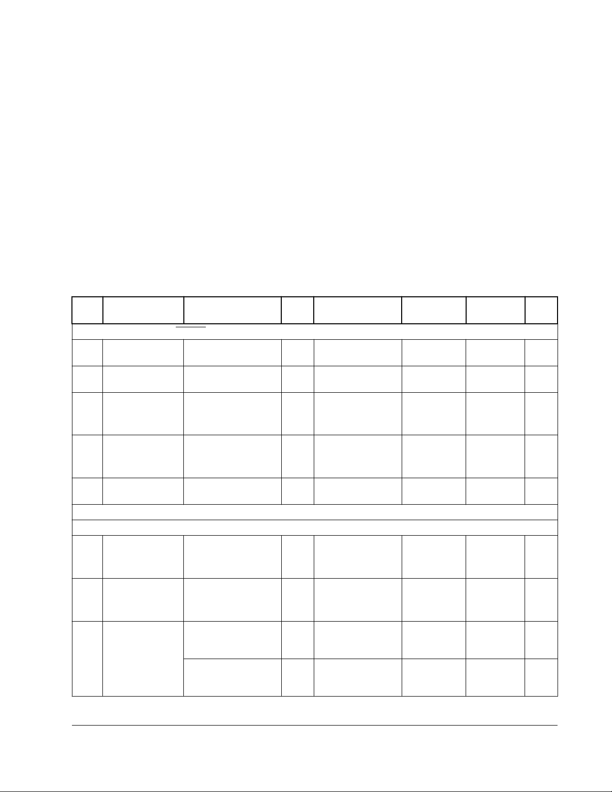
CPU Platform
ARM® Cortex-® M33
FPU
MPU
NVIC
DSP Accelerator
TrustZone® M
Fusion F1 DSP
DSP Processor
System Control
Security
SRAM PUF
AES-256
RNG
SHA-1/SHA-2
Upto 5 MB shared
low-leakage SRAM
192 KB ROM
Internal Memory
2x 32 KB FlexSPI Cache
16 KB USB RAM
FlexSPI(Quad/Octal) with
On-The-Fly OTFAD Decryption
External Memory
FlexSPI (Quad/Octal)
Connectivity
Analog Comparator
Analog
12-bit, 1MSPS ADC
2x Temp Sensor
Crypto Accelerators
Timers
(up to 200 MHz)
(up to 200 MHz)
2x PLL
FRO/OSC
PMC
Semaphore
Message unit
2x DMA
CRC engine
JTAG/SWD
System Tick Timers
Frequency Measure
OS/Event Timer
RTC
2x Watch Dog
5x Counter Timers
32-bit SCTimer/PWM
Multi-Rate Timer
Available on certain product families
FPU
Multimedia
2D GPU (up to 200 MHz)
MIPI®-DSI
(2 lane)
Display LCD
Controller
10x Frac rate gen
8-Ch DMIC
1x I2C
FlexIO
2xMIPI-I
3
GPIOs
2x HS SPI
2x SDIO/
eMMC/SD
Up to 9x Flexcomm
(UART/I2C/SPI/I2S)
HS USB Host/Device
+ DCD w/ PHY
The following table provides examples of orderable sample part numbers covered by this data sheet.
4
NXP Semiconductors
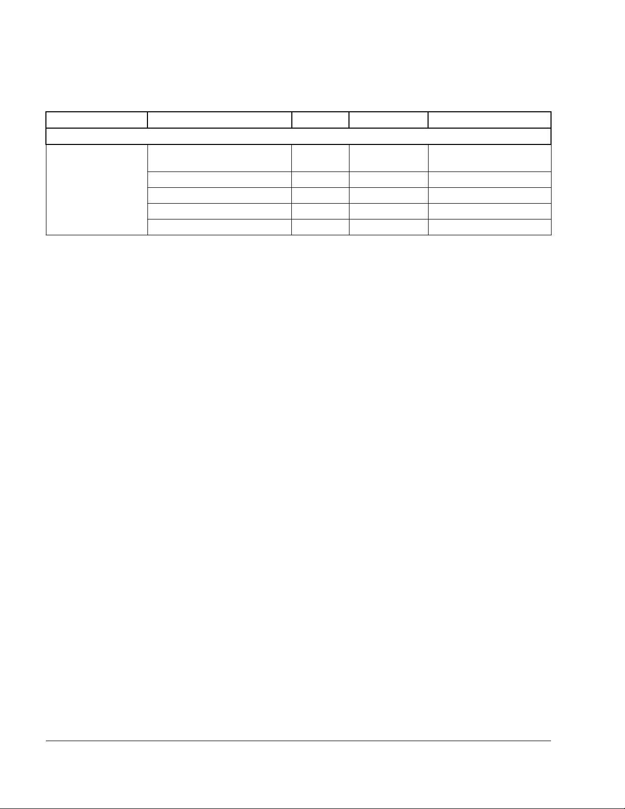
Figure 1. i.MX RT500 Block Diagram
i.MX RT500 Low-Power Crossover Processor, Rev. 0, 02/2021
Page 5
Orderable part number table
Orderable part
Part number
number
MIMXRT595SFFOC MRT595SFFOC 5 Yes Yes SRAM PUF, AES256,
MIMXRT555SFFOC MRT555SFFOC 5 No Yes SRAM PUF, AES256,
MIMXRT533SFFOC MRT533SFFOC 3 No No SRAM PUF, AES256,
MIMXRT595SFFOCR MRT595SFFOC 5 Yes Yes SRAM PUF, AES256,
MIMXRT555SFFOCR MRT555SFFOC 5 No Yes SRAM PUF, AES256,
MIMXRT533SFFOCR MRT533SFFOC 3 No No SRAM PUF, AES256,
MIMXRT533SFAWCR MRT533SFAWC 3 No No SRAM PUF, AES256,
MIMXRT555SFAWCR MRT555SFAWC 5 No Yes SRAM PUF, AES256,
MIMXRT595SFAWCR MRT595SFAWC 5 Yes Yes SRAM PUF, AES256,
1
SRAM
DSP Graphics Security USB I2S Package
(MB)
HASH
HASH
HASH
HASH
HASH
HASH
HASH
HASH
HASH
HS 9 FOWLP249
HS 9 FOWLP249
HS 9 FOWLP249
HS 9 FOWLP249
HS 9 FOWLP249
HS 9 FOWLP249
HS 6 WLCSP141
HS 6 WLCSP141
HS 6 WLCSP141
2
2
1. As marked on package
2. 249-pin Fan-out wafer-level package
Device revision number
Device Mask Set Number SILICONREV_ID JTAG_ID[CHIPREV]
2P43B 0x000B0002 0x2
Package markings for i.MX RT devices consist of 4 sets of identifiers as shown below.
i.MX RT500 Low-Power Crossover Processor, Rev. 0, 02/2021
5
NXP Semiconductors
Page 6
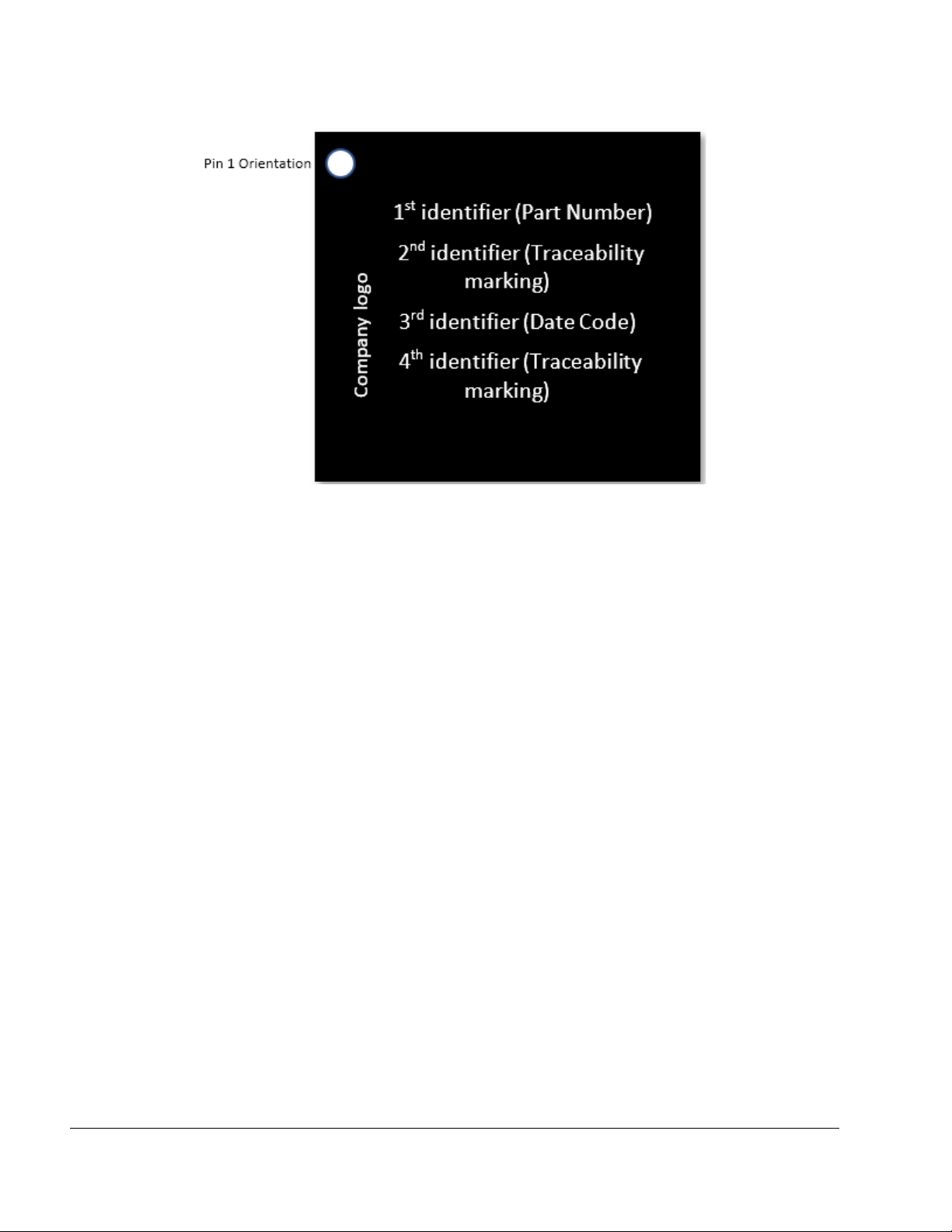
Figure 2. Package markings
• The 1st identifier defines the Part Number and is composed of 11 characters.
• The 2nd and 4th identifiers define the Traceability markings.
• The 3rd identifier defines the Date Code for the week of manufacture is a subset of the standard 5
character format.
The standard date code format is “xYYWW”:
• The leading digit represented by “x” can be ignored and “YYWW” indicate the Date Code.
• “YY" represents an encoding of the calendar year (for example, 19 corresponds to year 2019).
• “WW” represents an encoding of the work week within the calendar year (for example, 07 corresponds to
work week 7).
Please provide this information to your local NXP representative for further details.
The following figure explains the part number for this device.
6
NXP Semiconductors
i.MX RT500 Low-Power Crossover Processor, Rev. 0, 02/2021
Page 7
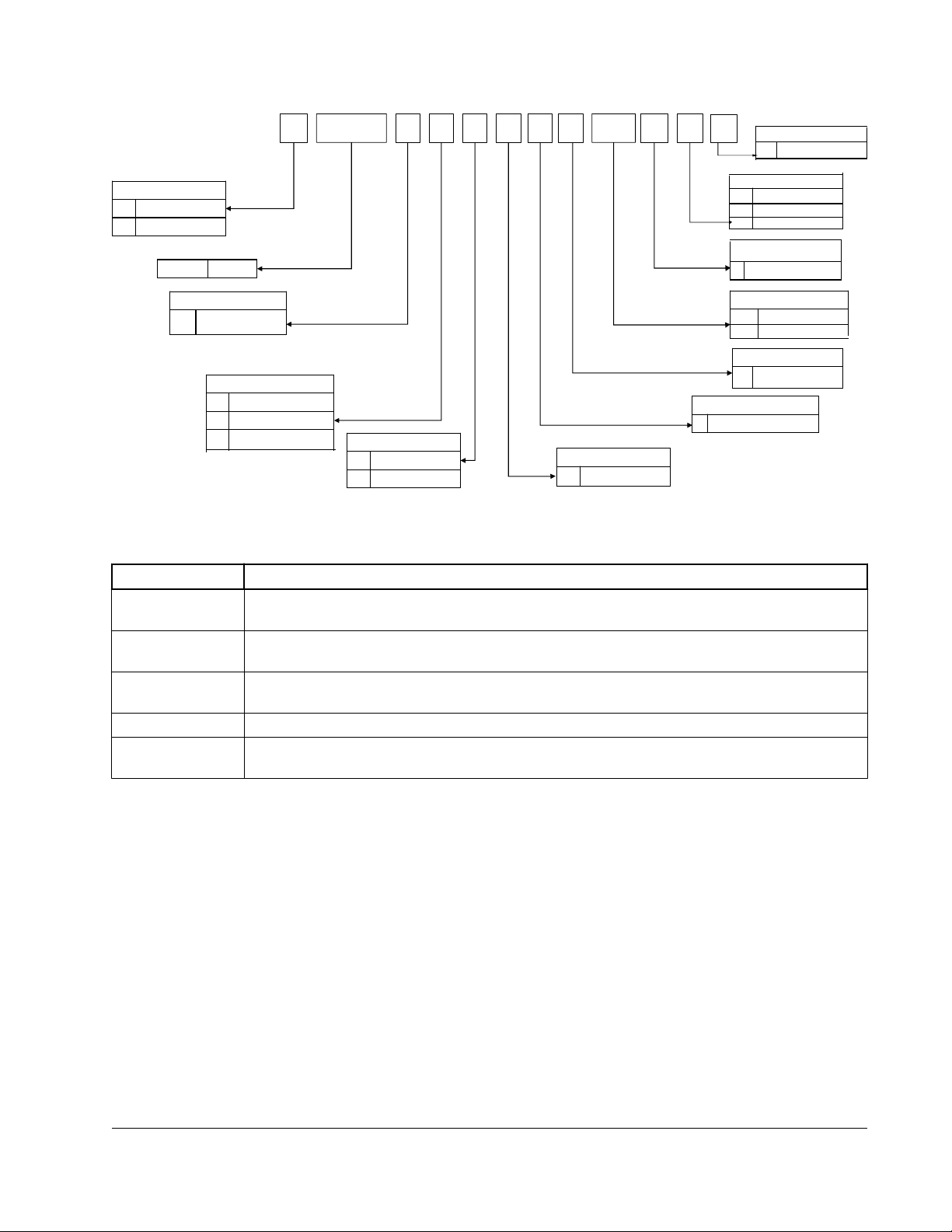
M IMXRT # # # # A AA x A
Qualification Level
M Mass Production
P Prototype
IMXRT Family
Series
5 RT500 series
Feature 2 (SRAM)
3 3MB
5 5MB
Feature 3
S Security
Temperature Range
F -20 – 70 C
Package
FO FOWLP 249
Silicon Revision
A Rev A
B
Rev B
Feature 1
3 no DSP, no Graphic
5 no DSP, w Graphic
w DSP, w Graphic
#
Feature 4 (Optional)
Speed/ Power
x
Reserved
Reserved
9
AW
WLCSP 141
Rev C
C
A
Packing Method
R
Reel
Figure 3. Part number diagram
Related Resources
Type Description
Selector Guide The Solution Advisor is a web-based tool that features interactive application wizards and a
dynamic product selector.
Product Brief The Product Brief contains concise overview/summary information to enable quick evaluation of a
device for design suitability.
Reference Manual The i.MX RT500 Low-Power Crossover MCU Reference Manual contains a comprehensive
description of the structure and function (operation) of a device.
Data Sheet Refers to this document which includes electrical characteristics and signal connections.
Chip Errata The chip mask set Errata provides additional or corrective information for a particular device mask
set.
i.MX RT500 Low-Power Crossover Processor, Rev. 0, 02/2021
7
NXP Semiconductors
Page 8

8
NXP Semiconductors
i.MX RT500 Low-Power Crossover Processor, Rev. 0, 02/2021
Page 9

Table of Contents
1 Electrical characteristics........................................................10
1.1 Chip-level conditions......................................................10
1.1.1 Thermal handling ratings................................. 10
1.1.2 Moisture handling ratings................................ 10
1.1.3 ESD handling ratings....................................... 11
1.1.4 Absolute maximum voltage and current
ratings..............................................................11
1.1.5 Thermal specifications..................................... 13
1.1.6 General operating conditions...........................14
1.1.7 I/O parameters.................................................17
1.1.8 Power consumption operating behavior.......... 19
1.1.9 CoreMark data................................................. 23
1.2 System power and clocks.............................................. 24
1.2.1 Power sequence.............................................. 24
1.2.2 Free-running oscillator FRO-192/96M
specifications................................................... 27
1.2.3 Crystal oscillator.............................................. 28
1.2.4 RTC oscillator.................................................. 29
1.2.5 External Clock Input (CLKIN) pin.....................29
1.2.6 Internal low-power oscillator (1 MHz).............. 29
1.3 System modules............................................................ 30
1.3.1 Reset timing parameters................................. 30
1.3.2 Serial Wire Debug (SWD) timing
specifications .................................................. 30
1.3.3 JTAG timing specifications.............................. 31
1.3.4 Wake-up process.............................................34
1.4 External memory interface.............................................35
1.4.1 FlexSPI Flash interface................................... 35
1.5 Display and graphics..................................................... 38
1.5.1 LCDIF.............................................................. 38
1.5.2 MIPI DSI timing................................................38
1.5.3 Flexible IO controller (FlexIO)..........................38
1.6 Analog characteristics....................................................39
1.6.1 12-bit ADC characteristics............................... 39
1.6.2 Temperature sensor........................................ 42
1.6.3 Comparator characteristics..............................43
1.7 Communication interfaces............................................. 45
1.7.1 USART interface..............................................45
1.7.2 I2C-bus............................................................ 46
1.7.3 I2S-bus interface............................................. 47
1.7.4 SPI interfaces (Flexcomm interfaces 0-8)....... 49
1.7.5 High-Speed SPI interface (Flexcomm
interface 14).....................................................51
1.7.6 SD/MMC and SDIO......................................... 53
1.7.7 DMIC subsystem............................................. 56
1.7.8 USB interface characteristics.......................... 57
1.7.9 USB DCD electrical specifications...................57
1.7.10 USB High Speed Transceiver and PHY
specifications................................................... 58
1.7.11 Improved Inter-Integrated Circuit Interface
(MIPI-I3C) specifications................................. 58
1.8 Timer modules............................................................... 60
1.8.1 SCTimer/PWM output timing........................... 61
2 Architectural overview...........................................................61
2.1 Detailed block diagram.................................................. 61
2.2 Shared system SRAM................................................... 62
2.3 RT500 modules list........................................................ 63
3 Application information..........................................................72
3.1 Current consumption vs. memory partitions.................. 72
3.2 Standard I/O pin configuration....................................... 73
3.3 I/O power consumption..................................................74
3.4 RTC oscillator................................................................ 74
3.4.1 RTC Printed Circuit Board (PCB) design
guidelines........................................................ 76
3.5 XTAL oscillator...............................................................76
3.5.1 XTAL Printed Circuit Board (PCB) design
guidelines........................................................ 78
3.5.2 Thermally compensated crystal oscillator
(TCXO)............................................................ 79
3.6 Suggested USB interface solutions............................... 79
4 Abbreviations........................................................................ 81
5 Pinouts.................................................................................. 81
5.1 Signal multiplexing and pinouts..................................... 81
5.2 i.MXRT500 Pinouts: 249 FOWLP package................... 82
5.3 i.MX RT500 Pinouts: 141 CSP package........................97
5.4 249-pin FOWLP and 141-pin WLCSP ballmaps............106
5.5 Termination of unused pins........................................... 107
5.6 Pin states in different power modes...............................108
5.7 Obtaining package dimensions......................................108
6 Power supply for pins............................................................108
7 Revision history.....................................................................110
i.MX RT500 Low-Power Crossover Processor, Rev. 0, 02/2021
9
NXP Semiconductors
Page 10
Electrical characteristics
Electrical characteristics
1
1.1 Chip-level conditions
This section provides the device-level electrical characteristics for the IC. See the
following table for a quick reference to the individual tables and sections.
Table 1. i.MX RT500 chip-level conditions
For these charateristics Topic appears
Absolute maximum voltage and current ratings Absolute maximum voltage and current ratings
Thermal handling ratings Thermal handling ratings
Moisture handling ratings Moisture handling ratings
ESD handling ratings ESD handling ratings
Thermal characteristics Thermal characteristics
General operating conditions General operating conditions
I/O parameters I/O parameters
Power consumption operating behavior Power consumption operating behavior
1.1.1 Thermal handling ratings
Symbol Description Min. Max. Unit Notes
T
STG
T
SDR
1. Determined according to JEDEC Standard JESD22-A103, High Temperature Storage Life.
2. Determined according to IPC/JEDEC Standard J-STD-020, Moisture/Reflow Sensitivity Classification for Nonhermetic
Solid State Surface Mount Devices.
Storage temperature — 150 °C 1
Solder temperature, lead-free — 260 °C 2
1.1.2 Moisture handling ratings
Symbol Description Min. Max. Unit Notes
MSL Moisture sensitivity level (FOWLP) — 3 — 1
MSL Moisture sensitivity level (WLCSP) — 1 — 1
1. Determined according to IPC/JEDEC Standard J-STD-020, Moisture/Reflow Sensitivity Classification for Nonhermetic
Solid State Surface Mount Devices.
10
NXP Semiconductors
i.MX RT500 Low-Power Crossover Processor, Rev. 0, 02/2021
Page 11
Electrical characteristics
1.1.3 ESD handling ratings
Symbol Description Min. Max. Unit Notes
V
HBM
V
CDM
I
LAT
1. Determined according to JEDEC Standard JESD22-A114, Electrostatic Discharge (ESD) Sensitivity Testing Human
Body Model (HBM).
2. Determined according to JEDEC Standard JESD22-C101, Field-Induced Charged-Device Model Test Method for
Electrostatic-Discharge-Withstand Thresholds of Microelectronic Components.
3. Determined according to JEDEC Standard JESD78, IC Latch-Up Test.
Electrostatic discharge voltage, human body model -2000 2000 V 1
Electrostatic discharge voltage, charged-device
model
Latch-up current at ambient temperature of 70 °C -100 100 mA 3
-500 500 V 2
1.1.4 Absolute maximum voltage and current ratings
Stress beyond those listed under the following table may
cause permanent damage to the device. These are stress
ratings only. Functional operation of the device at these or
any other conditions beyond those indicated under
“recommended operating conditions” is not implied.
Exposure to absolute-maximum-rated conditions for
extended periods may affect device reliability.
Table 2. Absolute maximum ratings1
Symbol Parameter Conditions Notes Min. Max. Unit
VDD_AO1V8 Supply 1.8 V
supply for
“always on”
features
VDD1V8 1.8 V supply
voltage for onchip analog
functions
other than the
ADC and
comparator.
VDD1V8_1 1.8 V supply
voltage for onchip digital
logic
Caution
- 2 -0.3 1.98 V
- 2 -0.3 1.98 V
- 2 -0.3 1.98 V
Table continues on the next page...
i.MX RT500 Low-Power Crossover Processor, Rev. 0, 02/2021
11
NXP Semiconductors
Page 12

Electrical characteristics
Table 2. Absolute maximum ratings1 (continued)
Symbol Parameter Conditions Notes Min. Max. Unit
VDDCORE 1.1 V input
supply for
core logic
VDDIO_0/1/2/4 Supply
voltage for
GPIO pins
VDDIO_3 Supply
voltage for
GPIO pins
VDDA_ADC1V8 1.8 V analog
supply voltage
for ADC and
comparator
VDDA_BIAS Bias voltage
for ADC and
comparator
VREFP ADC positive
reference
voltage
USB1_VDD3V3 USB1 analog
3.3 V supply
USB1_VBUS USB1_VBUS
detection
MIPI_DSI_VDD11 MIPI DSI 1.1
V PHY input
core voltage
supply
MIPI_DSI_VDD18 MIPI DSI 1.8
V PHY IO
input voltage
supply
MIPI_DSI_VDDA_CAP MIPI DSI 1.1
V capacitor
output voltage
supply
I
DD
supply current
(FOWLP249)
supply current
(WCLSP141)
On-chip regulator
not used.
LDO_ENABLE=0.
Power supplied
by an off-chip
power
management IC
(PMIC).
- 2 -0.3 1.98 V
- 2 -0.3 3.96 V
- 2 -0.3 1.98 V
- 2 -0.3 3.96 V
- 2 -0.3 1.98 V
- 2 -0.3 3.96 V
- - -0.3 5.6 V
- - -0.3 1.155 V
- - -0.3 1.98 V
- - -0.3 1.155 V
per supply pin,
1.71 V ≤ VDD <
3.6 V
per supply pin,
1.71 V ≤ VDD <
3.6 V
2 -0.3 1.155 V
3 - 100 mA
3 - 100 mA
12
NXP Semiconductors
Table continues on the next page...
i.MX RT500 Low-Power Crossover Processor, Rev. 0, 02/2021
Page 13

Table 2. Absolute maximum ratings1 (continued)
Symbol Parameter Conditions Notes Min. Max. Unit
I
I
latch
P
tot(pack)
SS
ground current
(FOWLP249)
ground current
(WLCSP141)
I/O latch-up
current
total power
dissipation
(per package)
total power
dissipation
(per package)
per ground pin,
1.71 V ≤ VDD <
3.6 V
per ground pin,
1.71 V ≤ VDD <
3.6 V
-(0.5VDD) < VI <
(1.5VDD);
Tj < 105 °C
FOWLP 249,
based on
package heat
transfer, not
device power
consumption
WLCSP141 - 1.42 W
Thermal specifications
3 - 100 mA
3 - 100 mA
- 100 mA
4 - 1.86 W
1. In accordance with the Absolute Maximum Rating System (IEC 60134). The following applies to the limiting values:
• This product includes circuitry specifically designed for the protection of its internal devices from the damaging
effects of excessive static charge. Nonetheless, it is suggested that conventional precautions be taken to avoid
applying greater than the rated maximum.
• Parameters are valid over operating temperature range unless otherwise specified. All voltages are with respect
to VSS unless otherwise noted.
• The limiting values are stress ratings only and operating the part at these values is not recommended and
proper operation is not guaranteed. The conditions for functional operation are specified in Table 1.
2. Maximum/minimum voltage above the maximum operating voltage (see Table 1) and below ground that can be
applied for a short time (< 10 ms) to a device without leading to irrecoverable failure. Failure includes the loss of
reliability and shorter lifetime of the device.
3. The peak current should not exceed the total supply current.
4. Determined in accordance to JEDEC JESD51-2A natural convection environment (still air).
1.1.5
1.1.5.1
Thermal specifications
Thermal operating requirements
Table 3. Thermal operating requirements
Symbol Description Min. Max. Unit Notes
T
j
T
A
Die junction
temperature
Ambient
temperature
-20 105 °C 1
-20 70 °C 1
1. Maximum TA can be exceeded only if the user ensures that TJ does not exceed maximum TJ. The simplest method to
determine TJ is: TJ = TA + R
i.MX RT500 Low-Power Crossover Processor, Rev. 0, 02/2021
× chip power dissipation.
ΘJA
NXP Semiconductors
13
Page 14
Thermal specifications
1.1.5.2 Thermal characteristics
The average chip junction temperature, Tj (°C), can be calculated using the following
equation:
(1)
• T
• R
= ambient temperature (°C),
amb
= the package junction-to-ambient thermal resistance (°C/W)
th(j-a)
• PD = sum of internal and I/O power dissipation
The internal power dissipation is the product of IDD and VDD. The I/O power dissipation
of the I/O pins is often small and many times can be negligible. However it can be
significant in some applications.
Table 4. Thermal resistance1
Symbol Parameter Conditions Max/Min Unit
249 FOWLP Package
R
R
R
R
th(j-a)
Ψ(JT)
th(j-a)
Ψ(JT)
thermal resistance from
junction to ambient
thermal resistance from
junction to package top
thermal resistance from
junction to ambient
thermal resistance from
junction to package top
JESD51-9, 2s2p, still
air
JESD51-9, 2s2p, still
air
141 WCLSP Package
JESD51-9, 2s2p, still
air
JESD51-9, 2s2p, still
air
29.6 °C/W
0.2 °C/W
35.3 °C/W
0.1 °C/W
1. Determined in accordance to JEDEC JESD51-2A natural convection environment (still air). Thermal resistance data in
this report is solely for a thermal performance comparison of one package to another in a standardized specified
environment. It is not meant to predict the performance of a package in an application-specific environment
1.1.6 General operating conditions
T
= -20 °C to +70 °C, unless otherwise specified.
amb
Table 5. General operating conditions
Symbol Parameter Conditions Min. Typ.
f
clk
14
NXP Semiconductors
CPU (CortexM33) clock
frequency
- - - 200 MHz
Table continues on the next page...
i.MX RT500 Low-Power Crossover Processor, Rev. 0, 02/2021
1
Max. Unit
Page 15

Table 5. General operating conditions (continued)
Symbol Parameter Conditions Min. Typ.
CPU (CortexM33) clock
frequency
f
clk
DSP clock
frequency
GPU clock
frequency
VDD_AO1V8 Supply 1.8 V
supply for
“always on”
features.
VDD1V8 1.8 V supply
voltage for onchip analog
functions other
than the ADC
and comparator
VDD1V8_1
2
1.8 V supply
voltage for onchip digital
logic
VDDCORE3, 4, 5, 61.1 V supply for
core logic. Onchip regulator
not used.
LDO_ENABLE
=0. Power
supplied by an
off-chip power
management
IC (PMIC).
VDDCORE
3
1.1 V supply for
core logic. Onchip regulator
not used.
LDO_ENABLE
=0. Power
supplied by an
off-chip power
management
IC (PMIC).
VDDIO_0/1/2/4 supply voltage
for GPIO rail
For USB high-speed device
90 - 200 MHz
and host operations
For OTP programming only - - 120 MHz
- - - 200 MHz
- - - 200 MHz
- 1.71 - 1.89 V
- 1.71 - 1.89 V
- 1.71 - 1.89 V
Retention mode 0.6 - 1.155 V
Active Mode (M33 Max
Freq = 60 MHz, FBB)
Active Mode (M33 Max
7
0.7 - - V
0.8 V
Freq = 100 MHz, FBB)
Active Mode (M33 Max
0.9 - - V
Freq = 192 MHz, FBB)
Active Mode (M33 Max
1.0 - - V
Freq = 230 MHz8, FBB)
Active Mode (M33 Max
1.1 - - V
Freq = 275 MHz8, FBB)
Retention mode 0.6 - 1.155 V
Active Mode (DSP Max
Freq = 60 MHz, FBB)
Active Mode (DSP Max
7
0.7 - - V
0.8 V
Freq = 100 MHz, FBB)
Active Mode (DSP Max
0.9 - - V
Freq = 192 MHz, FBB)
Active Mode (DSP Max
1.0 - - V
Freq = 230 MHz8, FBB)
Active Mode (DSP Max
1.1 - - V
Freq = 275 MHz8, FBB)
- 1.71 - 1.89 V
Thermal specifications
1
Max. Unit
Table continues on the next page...
i.MX RT500 Low-Power Crossover Processor, Rev. 0, 02/2021
15
NXP Semiconductors
Page 16

Thermal specifications
Table 5. General operating conditions (continued)
Symbol Parameter Conditions Min. Typ.
VDDIO_3 supply voltage
for GPIO rail
VDDA_1V8 1.8 V analog
supply voltage
for ADC and
comparator
VDDA_BIAS
9
Bias for ADC
and comparator
VREFP ADC positive
reference
voltage
USB1_VDD3V3 USB1 analog
3.3 V supply
USB0_VBUS USB0_VBUS
detection
MIPI_DSI_VDD11 MIPI DSI 1.1V
digital core
input voltage
supply
MIPI_DSI_VDD18 MIPI DSI 1.8V
PHY IO input
voltage supply
MIPI_DSI_VDDA_CAPMIPI DSI 1.1V
digital core
output voltage
supply
- 1.71 - 3.6 V
- 1.71 - 1.89 V
- 1.71 - 3.6 V
- 1.71 - 1.89 V
- 3.0 - 3.6 V
- 4.010 or 3.0
, 11
- 0.85 - 1.155 V
- 1.71 - 1.89 V
- -0.3 - 1.155 V
1
Max. Unit
5.0 5.5 V
1. Typical ratings are not guaranteed. The values listed are for room temperature (25 °C), nominal supply voltages.
2. 1.8 V supply voltage for on-chip digital logic during active mode. In deep-sleep mode, this pin can be powered off to
conserve additional current (~20 uA).
3. The maximum frequency for the specified VDDCORE voltage is the frequency of the main clock. This is before the CPU
CLOCK Divider. The VDDCORE voltage has to be set according to the chosen main clock frequency.
4. When LDO_ENABLE is externally tied low, the user must boot at VDDCORE = 1.0 V or higher (Low power/Normal clock
mode - OTP setting - BOOT_CLK_SPEED) or VDDCORE = 1.13 V (High Speed clock - OTP setting BOOT_CLK_SPEED). Thereafter, the VDDCORE can be adjusted to the desired level.
5. When LDO_ENABLE is externally tied high, the on-chip regulator to the VDDCORE Core voltage in PMC is set to the
default value 1.05 V (Low power/Normal clock mode - OTP setting - BOOT_CLK_SPEED) or 1.13 V (High Speed clock OTP setting - BOOT_CLK_SPEED). Thereafter, the POWER_SetLdoVoltageForFreq API function can be used to
internally configure the on-chip regulator voltage to the VDDCORE.
6. When performing any OTP read/write function, the VDDCORE voltage must be set to 1.0 V or higher when
LDO_ENABLE is externally tied high or low.
7. GPU, SPI, and CTIMER are disabled.
8. Although i.MX RT500 is targeted to operate up to 200 MHz for low power operation, it can operate up to 275 MHz;
however, there will be an increase in current consumption.
9. VDD_BIAS must be equal to maximum ADC input voltage or maximum comparator input voltage.
10. The USB PHY provides two options for reporting VBUS valid back to the USB controller:
• A programmable internal VBUS_VALID comparator (the default option), or
• An alternate VBUS_VALID_3V detector that will report VBUS valid for voltages above 3 V
16
i.MX RT500 Low-Power Crossover Processor, Rev. 0, 02/2021
NXP Semiconductors
Page 17
Thermal specifications
USBPHY_USB1_VBUS_DETECTn[VBUSVALID_SEL] selects which option is used. If the VBUS_VALID comparator is
used, USBPHY_USB1_VBUS_DETECTn[VBUSVALID_THRESH] determines the threshold voltage for a valid VBUS.
The programmable range is 4.0V to 4.4V (default).
11. The USB PHY provides two options for reporting VBUS valid back to the USB controller:
• A programmable internal VBUS_VALID comparator (the default option), or
• An alternate VBUS_VALID_3V detector that will report VBUS valid for voltages above 3 V
USBPHY_USB1_VBUS_DETECTn[VBUSVALID_SEL] selects which option is used. If the VBUS_VALID_3V detector
is used, the detector voltage is not programmable.
1.1.7 I/O parameters
1.1.7.1 I/O DC parameters
T
= -20 °C to +70 °C, unless otherwise specified. Values tested in production unless otherwise specified.
amb
Table 6. I/O DC characteristics
Sym
bol
VIHHIGH-level input
VILLOW-level input
VOHHIGH-level output
VOLLOW-level output
V
hys
IILLOW-level input
I
IH
Parameter Conditions Notes Min. Typ.
RESET pin, LDO_ENABLE pin, PMIC_IRQ_N pin, PMIC_MODE pins
0.7 x VDD_AO1V8 - VDD_AO1V8 V
voltage
-0.3 - 0.3 x
voltage
IOL = -2.9 mA;
voltage
voltage
hysteresis voltage 2 - 0.06 x
current
HIGH-level input
current
1.71 V ≤ VDD_AO1V8
< 1.89 V
IOL = 2.9 mA;
1.71 V ≤ VDD_AO1V8
< 1.89 V
Standard I/O pins and PMIC I2C pins
Input characteristics
VI = 0 V; on-chip pullup resistor disabled.
1.71 V ≤ VDD < 1.98 V
VI = 0 V; on-chip pull-
up resistor disabled.
3.0 V ≤ VDD < 3.6 V
VI = VDD; on-chip pull-
down resistor disabled.
1.71 V ≤ VDD < 1.98 V
VI = VDD; on-chip pull-
down resistor disabled.
3.0 V ≤ VDD < 3.6 V
0.8 x VDD_AO1V8 - - V
- - 0.2 x
-1 - 1 μA
-1 - 1 μA
-1 0.5 1 μA
-1 0.5 1 μA
VDD_AO1V8
1
Max. Unit
VDD_AO1V8
VDD_AO1V8
- V
V
V
Table continues on the next page...
i.MX RT500 Low-Power Crossover Processor, Rev. 0, 02/2021
17
NXP Semiconductors
Page 18
Thermal specifications
Table 6. I/O DC characteristics (continued)
Sym
Parameter Conditions Notes Min. Typ.
bol
VIinput voltage pin configured to
3
provide a digital
function, except the
following pins:
V
= 0 V
DDIO
VIHHIGH-level input
voltage
VILLOW-level input
voltage
V
hysteresis voltage 1.71 V ≤ VDD < 1.98 V 2 0.15 - - V
hys
1.71 V ≤ VDD < 1.98 V 0.7 x VDDIO - VDDIO V
3.0 V ≤ VDD ≤ 3.6 V 0.7 x VDDIO - VDDIO V
1.71 V ≤ VDD < 1.98 V -0.3 - 0.3 x VDDIO V
3.0 V ≤ VDD ≤ 3.6 V -0.3 - 0.7 V
0 - 3.6 V
3.0 V ≤ VDD ≤ 3.6 V 2 0.15 - - V
Output characteristics
V
HIGH-level output
OH
voltage (Normal
drive)
IOH = -2.9 mA;
1.71 V ≤ VDD < 1.98 V
IOH = -4 mA;
0.8 x VDDIO - - V
0.8 x VDDIO - - V
3.0 V ≤ VDD ≤ 3.6 V
V
HIGH-level output
OH
voltage (Full drive)
IOH = -5.8 mA;
1.71 V ≤ VDD < 1.98 V
IOH = -8 mA;
0.8 x VDDIO - - V
0.8 x VDDIO - - V
3.0 V ≤ VDD ≤ 3.6 V
VOLLOW-level output
voltage (Normal
Drive)
IOL = 2.9 mA;
1.71 V ≤ VDD < 1.98 V
IOL = 4 mA;
- - 0.2 x VDDIO V
- - 0.2 x VDDIO V
3.0 V ≤ VDD ≤ 3.6 V
LOW-level output
voltage (Full Drive)
IOL = 5.8 mA;
1.71 V ≤ VDD < 1.98 V
IOL = 8 mA;
- - 0.2 x VDDIO V
- - 0.2 x VDDIO V
3.0 V ≤ VDD ≤ 3.6 V
Weak input pull-up/pull-down characteristics
Ipdpull-down current VI = V
DD
34 - 180 μA
VI = 3.6 V 4 72 - 180 μA
Ipupull-up current VI = 0 V -34 - -180 μA
Rpdpull-down
20 - 50 kΩ
resistance
Rpupull-up resistance 20 - 50 kΩ
1
Max. Unit
1. Typical ratings are not guaranteed. The values listed are at room temperature (25 C), nominal supply voltage.
2. Guaranteed by design, not tested in production.
18
i.MX RT500 Low-Power Crossover Processor, Rev. 0, 02/2021
NXP Semiconductors
Page 19

Thermal specifications
3. All GPIO pins are fail safe up to 3.6 V when VDDIO supply = 0 V except following pins: PIO1_18 to PIO1_29, PIO1_30
to PIO1_31, PIO2_0 to PIO2_8, PIO2_24 to PIO2_31, PIO3_8 to PIO3_18, PIO4_11 to PIO4_17, and PIO5_15 to
PIO5_18.
4. Based on characterization. Not tested in production.
1.1.8 Power consumption operating behavior
NOTE
For the lowest power consumption, use the lowest SRAM
partition number.
T
= -20 °C to +70 °C, unless otherwise specified.
amb
Table 7. Power consumption in active mode
Symbol Parameter Conditions Notes Min. Typ.1,
Cortex M33 in Active mode, DSP no clock
enhanced while (1) code executed from SRAM partition 305; Internal LDO disabled
I
DDVDDCORE
VDDCORE supply
current
HCLK = 12 MHz
VDDCORE = 0.7 V
HCLK = 24 MHz
VDDCORE = 0.7 V
HCLK = 48 MHz
VDDCORE = 0.7 V
HCLK = 96 MHz
VDDCORE = 0.8 V
HCLK = 192 MHz
VDDCORE = 0.9 V
HCLK = 192 MHz
VDDCORE = 1.0 V
HCLK = 192 MHz
VDDCORE = 1.1 V
4
6 - 1.62 - mA
6 - 2.50 - mA
6 - 4.33 - mA
6 - 9.35 - mA
6 - 20.73 - mA
6 - 23.97 - mA
6 - 28.01 - mA
2, 3
Max. Unit
1. Typical ratings are not guaranteed. Typical values listed are at room temperature (25 °C). VDD_AO1V8 = VDD1V8 =
VDDIO_0/1/2/3/4 = VDDA_ADC1V8 = 1.8 V. VDDA_BIAS = VREFP = 1.8 V. USB1_VDD3V3 = 3.3
2. Characterized through bench measurements using typical samples.
3. Compiler settings: IAR C/C++ Compiler for Arm ver 8.40.1. High, Speed, No Size Constraints. The optimization level is
Low, Balanced.
4. Based on the power API library from the SDK software package available on nxp.com
5. SRAM partition 30 represents the worst case partition.
6. FRO clock source, FBB enabled
i.MX RT500 Low-Power Crossover Processor, Rev. 0, 02/2021
NXP Semiconductors
19
Page 20
Thermal specifications
T
= -20 °C to +70 °C, unless otherwise specified.
amb
Table 8. Power consumption in active mode
Symbol Parameter Conditions Min Typ1, 2,3Max Unit
Cortex M33 in Active mode, DSP no clock
CoreMark code executed from SRAM partition 30
I
DDVDDCORE
VDDCORE supply
current
HCLK = 12 MHz
VDDCORE = 0.7 V
HCLK = 24 MHz
4
5
- 1.61 - mA
- 2.51 - mA
VDDCORE = 0.7 V
HCLK = 48 MHz
- 4.26 - mA
VDDCORE = 0.7 V
HCLK = 96 MHz
- 9.28 - mA
VDDCORE = 0.8 V
HCLK = 192 MHz
- 20.44 - mA
VDDCORE = 0.9 V
HCLK = 192 MHz
- 23.73 - mA
VDDCORE = 1.0 V
HCLK = 192 MHz
- 27.87 - mA
VDDCORE = 1.1 V
1. Typical ratings are not guaranteed. Typical values listed are at room temperature (25 °C). VDD_AO1V8 = VDD1V8 =
VDDIO_0/1/2/3/4 = VDDA_ADC1V8 = 1.8 V. VDDA_BIAS = VREFP = 1.8 V. USB1_VDD3V3 = 3.3 V
2. Characterized through bench measurements using typical samples.
3. Compiler settings: IAR C/C++ Compiler for Arm ver 8.40. High Speed, No Size constraints. The optimization level is
Low, Balanced.
4. Based on the power API library from the SDK software package available on nxp.com
5. SRAM partition 30 represents the worst case partition.
T
= -20 °C to +70 °C, unless otherwise specified.
amb
Table 9. Power consumption in active mode
Symbol Parameter Conditions Notes Min Typ1, 2,
FFT code executed from SRAM partition 30 and 314; Internal LDO disabled
DSP in Active mode, M33 in WFI
I
DDVDDCORE
VDDCORE
supply current
20
NXP Semiconductors
5
HCLK = 10 MHz
6 - 1.80 - mA
VDDCORE = 0.7 V
HCLK = 40 MHz 6 5.30 mA
Table continues on the next page...
i.MX RT500 Low-Power Crossover Processor, Rev. 0, 02/2021
3
Max Unit
Page 21
Thermal specifications
Table 9. Power consumption in active mode (continued)
Symbol Parameter Conditions Notes Min Typ1, 2,
VDDCORE = 0.8 V
HCLK = 100 MHz
6 - 10.74 - mA
VDDCORE = 0.8 V
HCLK = 150 MHz
6 - 17.81 - mA
VDDCORE = 0.9 V
HCLK = 200 MHz
6 - 22.94 - mA
VDDCORE = 0.9 V
1. Typical ratings are not guaranteed. Typical values listed are at room temperature (25 °C). VDD_AO1V8 = VDD1V8 =
VDDIO_0/1/2/3/4 = VDDA_ADC1V8 = 1.8 V. VDDA_BIAS = VREFP = 1.8 V. USB1_VDD3V3 = 3.3 V
2. Characterized through bench measurements using typical samples.
3. Compiler settings: IAR C/C++ Compiler for Arm ver 8.40. High Speed, No Size constraints. The optimization level is
Low, Balanced.
4. SRAM partitions 30 and 31 represent the worst case partitions. The Fusion F1 DSP requires DRAM and IRAM in
different partitions. DSP_DRAM is in partition 30, DSP_IRAM is in partition 31.
5. Based on the power API library from the SDK software package available on nxp.com
6. PLL clock source, FBB enabled
3
Max Unit
Table 10. Power consumption in sleep mode
Symbol Parameter Conditions Notes Min. Typ. Max. Unit
Cortex-M33 in Sleep mode, DSP no clock
I
DDVDDCORE
supply
current
HCLK=12 MHz
VDDCORE=0.7 V
HCLK=12 MHz
VDDCORE=1.0 V
HCLK=24 MHz
VDDCORE=1.0 V
HCLK=48 MHz
VDDCORE=1.0 V
HCLK=96 MHz
VDDCORE=1.0 V
HCLK=192 MHz
VDDCORE=0.9 V
HCLK=192 MHz
VDDCORE=1.0 V
1. 256 KB SRAM, internal LDO enabled
2. All peripheral clocks gated
3. PLL disabled
4. FRO used as clock source
5. IAR C/C++ Compiler for Arm ver 8.4.2.1.236
1
2, 3, 4, 5 - 1.8 - mA
2, 3, 4, 5 - 4.27 - mA
2, 3, 4, 5 - 4.78 - mA
2, 3, 4, 5 - 5.78 - mA
2, 3, 4, 5 - 7.78 - mA
2, 3, 4, 5 - 9.66 - mA
2, 3, 4, 5 - 11.74 - mA
T
= -20 °C to +70 °C, unless otherwise specified.
amb
i.MX RT500 Low-Power Crossover Processor, Rev. 0, 02/2021
21
NXP Semiconductors
Page 22
Thermal specifications
Table 11. Power consumption in deep sleep mode
Symbol Parameter Conditions NotesMin Typ1,
2
Max
3
Unit
I
VDD1V8
I
VDDCORE
I
VDDCORE
I
VDDCORE
supply
current
supply
current
supply
current
supply
current
Deep-sleep mode; SRAM (128 KB) powered, Internal
LDO disabled. Array On, Periphery Off
Deep-sleep mode; SRAM (32 KB) powered, Internal
LDO disabled. Array On, Periphery Off
T
= 25 °C
amb
Deep-sleep mode; SRAM (32 KB) powered, Internal
LDO disabled. Array On, Periphery Off
T
= 70 °C
amb
Deep-sleep mode; SRAM (128 KB) powered, Internal
LDO disabled. Array On, Periphery Off
T
= 25 °C
amb
Deep-sleep mode; SRAM (128 KB) powered, Internal
LDO disabled. Array On, Periphery Off
T
= 70 °C
amb
Deep-sleep mode; SRAM (5 MB) powered, Internal
LDO disabled. Array On, Periphery Off
T
= 25 °C
amb
Deep-sleep mode; SRAM (5 MB) powered, Internal
LDO disabled. Array On, Periphery Off
T
=70 °C
amb
4 - 8.5 - μA
4 - 40.7 - μA
4 - 200 μA
4 - 42.0 - μA
4 - 210 - μA
4 - 74 120 μA
4 - 432 - μA
1. Typical ratings are not guaranteed. Typical values listed are at room temperature (25 °C). All power supplies = 1.8 V,
except USB1_VDD3V3=3.3 V
2. Characterized through bench measurements using typical samples.
3. Guaranteed by characterization, not tested in production.
4. VDDCORE = 0.6 V, RBB Enabled
T
= -20 °C to +70 °C, unless otherwise specified.
amb
Table 12. Power consumption in deep sleep mode
Symbol Parameter Conditions Min Typ1,
I
VDD_AO1V
8
I
VDDIO_0
supply current Deep-sleep mode; SRAM (128 KB) powered, Internal
LDO disabled. Array On, Periphery Off
supply current Deep-sleep mode; SRAM (128 KB) powered, Internal
- 0.79 - μA
- 2.4 - μA
LDO disabled. Array On, Periphery Off
I
VDDIO_1
supply current Deep-sleep mode; SRAM (128 KB) powered, Internal
- 1.7 - μA
LDO disabled. Array On, Periphery Off
I
VDDIO_2
supply current Deep-sleep mode; SRAM (128 KB) powered, Internal
- 0.35 - μA
LDO disabled. Array On, Periphery Off
I
VDDIO_3
supply current Deep-sleep mode; SRAM (128 KB) powered, Internal
- 0.8 - μA
LDO disabled. Array On, Periphery Off
I
VDDIO_4
supply current Deep-sleep mode; SRAM (128 KB) powered, Internal
- 0.36 - μA
LDO disabled. Array On, Periphery Off
Table continues on the next page...
2
Max
3
Unit
22
NXP Semiconductors
i.MX RT500 Low-Power Crossover Processor, Rev. 0, 02/2021
Page 23
Thermal specifications
Table 12. Power consumption in deep sleep mode (continued)
Symbol Parameter Conditions Min Typ1,
I
VDDA_1V8
supply current Deep-sleep mode; SRAM (128 KB) powered, Internal
- 11.8 - μA
2
LDO disabled. Array On, Periphery Off
I
VREFP
supply current Deep-sleep mode; SRAM (128 KB) powered, Internal
- 0.02 - μA
LDO disabled. Array On, Periphery Off
I
USB1_VDD
3V3
supply current Deep-sleep mode; SRAM (128 KB) powered, Internal
LDO disabled. Array On, Periphery Off
- 1.10 - μA
1. Typical ratings are not guaranteed. Typical values listed are at room temperature (25 °C). All power supplies = 1.8 V,
except USB1_VDD3V3=3.3 V
2. Characterized through bench measurements using typical samples.
3. Guaranteed by characterization, not tested in production.
T
= -20 °C to +70 °C, unless otherwise specified.
amb
Max
3
Unit
Table 13. Power consumption in deep power-down mode and full deep power-down modes
Symbol Parameter Conditions Min Typ1,
I
VDD_AO1
V8
supply current Full Deep power-down mode; Internal LDO disabled.
RTC Off
T
= 25 °C
amb
Full Deep power-down mode; Internal LDO disabled.
- 0.51 - μA
- 1.79 - μA
RTC Off
T
= 70 °C
amb
I
VDDIO_0
supply curent Deep power-down mode; Internal LDO disabled. RTC
- 2.4 - μA
Off
I
VDDIO_1
supply current Deep power-down mode; Internal LDO disabled. RTC
- 1.68 - μA
Off
I
VDDIO_2
supply current Deep power-down mode; Internal LDO disabled. RTC
- 0.45 - μA
Off
I
VDDIO_3
supply current Deep power-down mode; Internal LDO disabled. RTC
- 0.37 - μA
Off
I
VDDIO_4
supply current Deep power-down mode; Internal LDO disabled. RTC
- 0.44 - μA
Off
I
VDD1V8
supply current Deep power-down mode; Internal LDO disabled. RTC
- 7.8 - μA
Off
I
VREFP
supply current Deep power-down mode; Internal LDO disabled. RTC
- 0.01 - μA
Off
I
USB1_VDD
3V3
supply current Deep power-down mode; Internal LDO disabled. RTC
Off
- 1.1 - μA
2
Max
3
Unit
1. Typical ratings are not guaranteed. Typical values listed are at room temperature (25 °C). All power supplies = 1.8 V,
except USB1_VDD3V3=3.3V
2. Characterized through bench measurements using typical samples.
3. Guaranteed by characterization, not tested in production.
i.MX RT500 Low-Power Crossover Processor, Rev. 0, 02/2021
NXP Semiconductors
23
Page 24
Thermal specifications
1.1.9 CoreMark data
Table 14. Coremark data
Parameters Conditions Notes Typ.1, 2,
ARM Cortex-M33 in active mode
CoreMark Score CoreMark code executed from
SRAM; HCLK = 12 MHz
HCLK = 24 MHz 4 3.85 (Iterations/s) / MHz
HCLK = 48 MHz 4 3.85 (Iterations/s) / MHz
HCLK = 96 MHz 5 3.85 (Iterations/s) / MHz
HCLK = 192 MHz 5 3.85 (Iterations/s) / MHz
1. Characterized through bench measurements using typical samples.
2. Compiler settings: IAR C/C++ Compiler for Arm ver 8.22.2, optimization level 3, optimized for time on.
3. VDD_AO1V8 = VDD1V8 = VDDIO_0/1/2/3/4 = VDDA_ADC1V8 = VREFP = 1.8 V. VDDA_BIAS = USB1_VDD3V3 = 3.3
V
4. Clock source FRO. PLL disabled
5. Clock source external clock to XTALIN (bypass mode). PLL enabled.
4 3.85 (Iterations/s) / MHz
3
Unit
1.2 System power and clocks
1.2.1 Power sequence
Following power-on sequence should be followed when using the internal LDO in i.MX
RT500:
1. VDD_AO1V8, VDD1V8, and VDD1V8_1 pins should be powered first. There is
no power sequence requirement between powering the VDD_AO1V8 and
VDD1V8 pins.
2. VDDA_ADC1V8 and VREFP can be powered concurrently with VDD_AO1V8
and VDD1V8 or later
3. VDDIO_x and VDDA_BIAS pins can be powered concurrently with
VDD_AO1V8 and VDD1V8 if these pins are 1.8 V range or later if these pins are
3.3 V range. If the VDDIO_x is not powered concurrently with the VDD1V8, the
delta voltage between VDDIO_x and VDD1V8 must be 1.89 V or less.
The VDDCORE pin will be supplied from the internal LDO and the LDO is powered
from the VDD1V8. An external capacitor (4.7 uF) must be connected on the
VDDCORE pin. USB1_VDD3V3 can be powered at any time, independent of the other
supplies.
24
NXP Semiconductors
i.MX RT500 Low-Power Crossover Processor, Rev. 0, 02/2021
Page 25

Thermal specifications
Following power-on sequence should be followed when using an external PMIC or
external IC to drive the VDDCORE pin (internal LDO is disabled, see timing diagram
below):
1. VDD_AO1V8, VDD1V8, and VDD1V8_1 pins should be powered first. There is
no power sequence requirement between powering the VDD_AO1V8 and
VDD1V8 pins.
2. VDDA_ADC1V8 and VREFP can be powered concurrently with VDD_AO1V8
and VDD1V8 or later.
3. VDDIO_x and VDDA_BIAS pins can be powered concurrently with VDD1V8 if
these pins are 1.8 V range or later if these pins are 3.3 V range. If the VDDIO_x
is not powered concurrently with the VDD1V8, the delta voltage between
VDDIO_x and VDD1V8 must be 1.89 V or less.
4. Power up the VDDCORE. The external RESETN should be held low until
VDDCORE is valid in the timing diagram.VDDCORE should not be ramped up
until after all the other supplies have completed ramp up.
USB1_VDD3V3 can be powered at any time, independent of the other supplies.
Sequence of operations is handled internally so there is no specific timing requirement
between the supplies. The time delays caused by any of the bypass capacitors will
have no effect on the operation of the part. The internal POR detectors on
VDD_AO1V8, VDD1V8 pins, and the Low Voltage Detector on VDDCORE pin,
require a fall time of at least 10us (preliminary) to trigger. There is no restriction on
the rise time, except for the sequencing defined above.
Table 15. Power-on characteristics
Symbol Timing
Parameter
A VDDIO_x valid to
VDDCORE valid
B VDDCORE valid to
De-assertion of
RESETN
AA Mode pin valid When the mode
Description Min. Max. Unit
The delay from
when the IO pad
voltages become
valid to core
voltage valid
The delay from
when the VDD
core is valid to
when the RESETN
can be released
pins becomes
valid. On power-
on, the mode pins
are reset to 00 and
are controlled via a
10 - μs
20 - μs
- 2 μs
i.MX RT500 Low-Power Crossover Processor, Rev. 0, 02/2021
25
NXP Semiconductors
Page 26

Thermal specifications
Table 15. Power-on characteristics
Symbol Timing
Parameter
Description Min. Max. Unit
POR circuit in the
always-on domain.
The timing is from
when the
VDD_AO1V8 is
valid to when the
mode pins are
reset to 00.
26
NXP Semiconductors
i.MX RT500 Low-Power Crossover Processor, Rev. 0, 02/2021
Page 27
VDDIO_2
(Pad group 2 power)
VDDIO_3
(Pad group 3 power)
VDDIO_4
(Pad group 4 power)
VDDCORE
(Core Power needs DVFS
control)
VDDA_ADC1V8
(ADC/Comp power 1.8 volts)
VREFP
(ADC Ref voltage)
RESETN
(External Chip reset)
PMIC_MODE0/1
(PMIC Mode pins (outputs))
XXXXXXXXX
00
VDD_AO_1V8
(Always on voltage to RTC)
VDD1V8
(Chip PMC power)
A B
AA
VDDA_BIAS
(ADC comparator bias)
VDDIO_0
(Pad group 0 power)
VDDIO_1
(Pad group 1 power)
Thermal specifications
Figure 4. Power-up ramp
1.2.2
Free-running oscillator FRO-192/96M specifications
Table 16. FRO-192M specifications
Symbol Characteristic Min. Typ. Max. Unit
f
fro192m
Δf
fro192m
FRO-192M frequency (nominal) 192 MHz
Frequency deviation
• 1T trim (Open loop)
— — ±1 %
Table continues on the next page...
%
i.MX RT500 Low-Power Crossover Processor, Rev. 0, 02/2021
27
NXP Semiconductors
Page 28
Thermal specifications
Table 16. FRO-192M specifications (continued)
Symbol Characteristic Min. Typ. Max. Unit
t
startup
Start-up time
— 75 — μs
jit
cyc
I
fro192m
V
min
Cycle to cycle jitter — 105 — ps
Current consumption — 45 111 μA
Minimum voltage 0.8
1
— — V
1. Vmin =0.8 V is derived from FRO192 MHz divided by 2/4/8.
NOTE
Any divided versions of the FRO that are not being used
anywhere should be turned off to save power.
Table 17. FRO-96M specifications
Symbol Characteristic Min. Typ. Max. Unit
f
fro96m
Δf
t
startup
jit
I
fro96m
V
fro96m
cyc
min
FRO-96M frequency (nominal) 96 MHz
Frequency deviation
• 1T trim (Open loop)
Start-up time
— — ±1 %
— 120 — μs
Cycle to cycle jitter — 180 — ps
Current consumption — 23 63 μA
Minimum voltage 0.7
1
— — V
%
1. Vmin =0.7 V is derived from FRO96 MHz divided by 2/4/8.
1.2.3 Crystal oscillator
T
= -20 °C to +70 °C; 1.71 V ≤ V
amb
≤ 1.89 V.1,
DD
Table 18. Crystal oscillator characteristics
Symbol Parameter Min. Typ.
f
range
Rf feedback resistor
ESR Equivalent series
1. Parameters are valid over operating temperature range unless otherwise specified.
2. See XTAL oscillator
3. Typical ratings are not guaranteed. The values listed are at room temperature (25 °C), nominal supply voltages.
28
NXP Semiconductors
oscillator frequency
range
high gain mode
4
only
resistance
2
3
Max. Unit
4 - 32 MHz
- 1 - MΩ
- - 80 Ω
i.MX RT500 Low-Power Crossover Processor, Rev. 0, 02/2021
Page 29
Thermal specifications
4. CLKCTL0_SYSOSCCTL0[LP_ENABLE] = 1 sets High Gain Mode, which requires a 1 MΩ feedback resistor.
1.2.4 RTC oscillator
See RTC oscillator for connecting the RTC oscillator to an external clock source.
T
= -20 °C to +70 °C; 1.71 ≤ V
amb
Table 19. RTC oscillator characteristics
Symbol Parameter Conditions Min. Typ.
f
input frequency - - 32.768 - kHz
1
ESR Equivalent series
resistance
, 2
t
start_xtal
t
start_bypass
V
Crystal oscillator
start-up time
Bypass oscillator
2
start-up time
3
Peak-to-Peak
pp
amplitude of
oscillation
- - 50 100K kΩ
- - 250 - ms
With oscillator
bypass mode
enabled
DD
≤ 1.89
1
1 - ms
0.7 - VDD_AO1V8 V
Max. Unit
1. Typical ratings are not guaranteed. The values listed are at room temperature (25 C), nominal supply voltages.
2. Proper PCB layout procedures must be followed to achieve specifications.
3. In bypass mode, using an input square wave only on RTCXIN with RTXOUT floating.
1.2.5 External Clock Input (CLKIN) pin
T
= -20 °C to +70 °C; 1.71 V to 1.89 V
amb
Table 20. Dynamic characteristic: CLKIN
Symbol Parameter Conditions Min. Typ.
F
i
1. Typical ratings are not guaranteed. The values listed are at room temperature (25 °C), nominal supply voltages
input frequency - - - 50 MHz
1
Max Unit
1.2.6 Internal low-power oscillator (1 MHz)
The IRC is trimmed to 10% accuracy over the entire voltage and temperature range.
T
= -20 °C to +70 °C; 1.71 ≤ V
amb
i.MX RT500 Low-Power Crossover Processor, Rev. 0, 02/2021
≤ 1.89 V
DD
29
NXP Semiconductors
Page 30

RESETN
CC1
(Input)
Thermal specifications
Table 21. LPOSC characteristics
Symbol Parameter Conditions Min Typ
f
osc (RC)
1. Typical ratings are not guaranteed. The values listed are at room temperature (25 °C), nominal supply voltages.
LPOSC clock
frequency
- 0.9 1 1.1 MHz
1
Max Unit
1.3 System modules
1.3.1 Reset timing parameters
The following figure shows the reset timing and Table 22 lists the timing parameters.
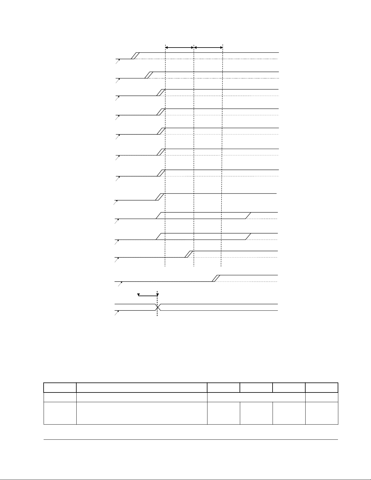
Figure 5. Reset timing diagram
Table 22. Reset timing parameters
ID Parameter Min Max Unit
CC1 Duration of POR_B to
be qualified as valid
40 - ns
1.3.2 Serial Wire Debug (SWD) timing specifications
Table 23. SWD timing specifications
Symbol Description Min. Max. Min.—
VLPR
mode
J1 SWD_CLK frequency of operation
J2 SWD_CLK cycle period 1000/J1 — 1000/J1 — ns
J3 SWD_CLK clock pulse width
• Serial wire debug
0 25 0 10 MHz
20 — 20 — ns
Max.—
VLPR
mode
Unit
J4 SWD_CLK rise and fall times — 3 — 3 ns
Table continues on the next page...
30
NXP Semiconductors
i.MX RT500 Low-Power Crossover Processor, Rev. 0, 02/2021
Page 31
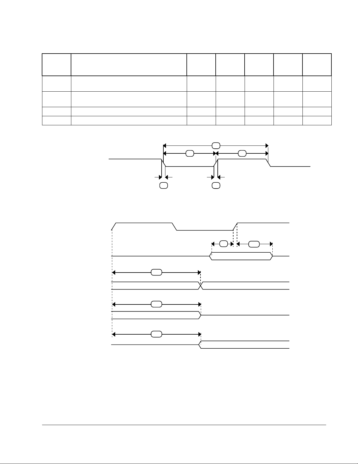
Table 23. SWD timing specifications (continued)
J2
J3 J3
J4 J4
SWD_CLK (input)
J11
J12
J11
J9
J10
Input data valid
Output data valid
Output data valid
SWD_CLK
SWD_DIO
SWD_DIO
SWD_DIO
SWD_DIO
Thermal specifications
Symbol Description Min. Max. Min.—
VLPR
mode
J9 SWD_DIO input data setup time to SWD_CLK
rise
J10 SWD_DIO input data hold time after SWD_CLK
rise
J11 SWD_CLK high to SWD_DIO data valid — 37 — 37 ns
J12 SWD_CLK high to SWD_DIO high-Z 2 — 2 — ns
10 — 19 — ns
0 — 0 — ns
Max.—
VLPR
mode
Figure 6. Serial wire clock input timing
Unit
i.MX RT500 Low-Power Crossover Processor, Rev. 0, 02/2021
Figure 7. Serial wire data timing
31
NXP Semiconductors
Page 32

J2
J3 J3
J4 J4
TCLK (input)
Thermal specifications
1.3.3 JTAG timing specifications
Table 24. JTAG timing specifications
Symbol Parameter Min. Max. Min.—
VLPR
mode
J1 TCLK frequency of operation
• Boundary Scan 0 10 0 10 MHz
• JTAG 0 25 0 10 MHz
J2 TCLK cycle period 1000/J1 — 1000/J1 — ns
J3 TCLK clock pulse width
• Boundary Scan 50 — 50 — ns
• JTAG 20 — 20 — ns
J4 TCLK rise and fall times — 3 — 3 ns
J5 Boundary scan input data setup time to TCLK
rise
J6 Boundary scan input data hold time after TCLK
rise
J7 TCLK low to boundary scan output data valid — 28 — 28 ns
J8 TCLK low to boundary scan output high-Z — 25 — 25 ns
J9 TMS, TDI input data setup time to TCLK rise 10.5 — 19 — ns
J10 TMS, TDI input data hold time after TCLK rise 2.5 — 2 — ns
J11 TCLK low to TDO data valid — 19 — 19 ns
J12 TCLK low to TDO high-Z 2 — 2 — ns
J13 TRST assert time 100 — 100 — ns
J14 TRST setup time (negation) to TCLK high 8 — 8 — ns
20 — 20 — ns
5 — 5 — ns
Max.—
VLPR
mode
Unit
32
NXP Semiconductors
Figure 8. Test clock input timing
i.MX RT500 Low-Power Crossover Processor, Rev. 0, 02/2021
Page 33

J7
J8
J7
J5
J6
Input data valid
Output data valid
Output data valid
TCLK
Data inputs
Data outputs
Data outputs
Data outputs
J11
J12
J11
J9
J10
Input data valid
Output data valid
Output data valid
TCLK
TDI/TMS
TDO
TDO
TDO
Thermal specifications
Figure 9. Boundary scan (JTAG) timing
i.MX RT500 Low-Power Crossover Processor, Rev. 0, 02/2021
Figure 10. Test Access Port timing
33
NXP Semiconductors
Page 34

J14
J13
TCLK
TRST
Thermal specifications
1.3.4 Wake-up process
Figure 11. TRST timing
VDD = 3.3 V;T
= 25 °C; using FRO as the system clock.
amb
Table 25. Typical wake-up times from low power modes
Symbol Parameter Conditions Notes Min. Typ.
t
wake
t
wake
t
wake
wake-up time from sleep
mode, 200
MHz
wake-up time from deep-
sleep mode,
using
RESETN.
from deepsleep mode,
using
PMIC_IRQ_N
.
wake-up time from full deep
power-down
mode, using
RESETN
from full deep
power-down
mode, using
PMIC_IRQ_N
2, 3 - 150 - μs
4 - 120 - μs
4 - 120 - μs
4 - 8.64 - ms
4 - 8.64 - ms
1
Max. Unit
1. Typical ratings are not guaranteed. The values listed are at room temperature (25 C), nominal supply voltages.
2. The wake-up time measured is the time between when a GPIO input pin is triggered to wake the device up from the low
power modes and from when a GPIO output pin is set in the interrupt service routine (ISR) wake-up handler.
3. FRO disbled, all peripherals off. PLL disabled.
4. Wake up from deep power-down causes the part to go through entire reset process. The wake-up time measured is the
time between when the Wake-Up pin is triggered to wake the device up and when a GPIO output pin is set in the reset
handler.
34
NXP Semiconductors
i.MX RT500 Low-Power Crossover Processor, Rev. 0, 02/2021
Page 35

External memory interface
1.4
External memory interface
1.4.1 FlexSPI Flash interface
Tamb = -20 °C to +70 °C, VDDIO_x = 1.71 V to 1.89 V; VDDCORE = 1.13 V; CL =
5 pF balanced loading on all pins; Full Drive Mode on all pins, Input slew = 1 ns,
SLEW setting = standard mode for all pins; Parameters sampled at the 50 % level of
the rising or falling edge.
Table 26. Dynamic characteristics: FlexSPI flash interface1
Symbol Parameter Conditions Min. Typ. Max. Unit
SDR mode
f
clk
t
DS
t
DH
t
V(Q)
DDR Mode (with and without DQS)
f
clk
clock frequency Transmit — — 200 MHz
RX clock source = 0 — — 60 MHz
RX clock source = 1 — — 116 MHz
RX clock source = 3 — — 200 MHz
data set-up time RX clock source = 0
(internal dummy read
strobe and loopbacked
internally)
RX clock source = 1
(internal dummy read
strobe and loopbacked
from DQS pad)
source = 3 (external
DQS, Flash provides
read strobe)
data hold time RX clock source = 0
(internal dummy read
strobe and loopbacked
internally)
RX clock source = 1
(internal dummy read
strobe and loopbacked
from DQS pad)
source = 3 (external
DQS, Flash provides
read strobe)
data output valid
time
clock frequency Transmit — — 200 MHz
Table continues on the next page...
6 — — ns
1 — — ns
0 — 0.6 ns
1 — — ns
0 — — ns
0 — — ns
0 — 3 ns
i.MX RT500 Low-Power Crossover Processor, Rev. 0, 02/2021
35
NXP Semiconductors
Page 36

t
DStDH
fclk
t
DStDH
nternal Sample Clock
IO[0:7]
External memory interface
Table 26. Dynamic characteristics: FlexSPI flash interface1 (continued)
Symbol Parameter Conditions Min. Typ. Max. Unit
RX clock source = 0 — — 30 MHz
RX clock source = 1 — — 58 MHz
t
DS
t
DH
t
V(Q)
RX clock source = 3, with
external DQS.
data set-up time RX clock source = 0
(internal dummy read
strobe and loopbacked
internally)
RX clock source = 1
(internal dummy read
strobe and loopbacked
from DQS pad)
source = 3 (external
DQS, Flash provides
read strobe)
data hold time RX clock source = 0
(internal dummy read
strobe and loopbacked
internally)
RX clock source = 1
(internal dummy read
strobe and loopbacked
from DQS pad)
source = 3 (external
DQS, Flash provides
read strobe)
data output valid
time
— — 200 MHz
6 — — ns
1 — — ns
0 — 0.6 ns
1 — — ns
0 — — ns
0 — — ns
0 — — ns
1. Based on simulation; not tested in production.
Following are the FlexSPI timing diagrams for SDR and DDR input and output timing
modes.
Figure 12. SDR mode (input timing, mode 0 and 1)
36
NXP Semiconductors
i.MX RT500 Low-Power Crossover Processor, Rev. 0, 02/2021
Page 37

tDSt
DH
DQS
IO[0:7]
tDSt
DH
nternal Sample Clock
T
CLK
t
V(Q)max
t
V(Q)min
t
t
fclk
V(Q)max
V(Q)min
T
CLK
t
V(Q)max
t
V(Q)min
t
t
DQS
IO[0:7]
V(Q)max
V(Q)min
t
DStDH
t
DStDH
IO[0:7]
fclk
tDSt
DH
t
DStDH
IO[0:7]
DQS
External memory interface
Figure 13. SDR mode (input timing, mode 3)
Figure 14. SDR mode (output timing, mode 0 and 1)
i.MX RT500 Low-Power Crossover Processor, Rev. 0, 02/2021
Figure 15. SDR mode (output timing, mode 3)
Figure 16. DDR mode (input timing, mode 0 and 1)
Figure 17. DDR mode (input timing, mode 3)
37
NXP Semiconductors
Page 38

T
CLK
t
V(Q)min
t
t
V(Q)min
fclk
V(Q)max
t
V(Q)max
T
CLK
t
V(Q)max
t
V(Q)min
t
V(Q)max
t
IO[0:7]
DQS
V(Q)min
External memory interface
Figure 18. DDR mode (output timing, mode 0 and 1)
Figure 19. DDR mode (output timing, mode 3)
1.5
Display and graphics
1.5.1 LCDIF
T
= -20 °C to 70 °C; VDD = 2.7 V to 3.6 V; CL = 30 pF. Simulated values.
amb
Table 27. LCDIF characteristics
Symbol Parameter Conditions Min. Typ. Max. Unit
f
t
v(Q)
clk
clock frequency on pin LCD_DCLK - - 60 MHz
data output valid time on all LCD output pins 0.3 - 4.5 ns
1.5.2 MIPI DSI timing
The i.MX RT500 conforms to the MIPI D-PHY electrical specifications MIPI DSI
Version 1.01 and D-PHY specification Rev. 1.0 (and also DPI version 2.0, DBI version
2.0, DSC version 1.0a at protocol layer) for MIPI display port x2 lanes.
38
NXP Semiconductors
i.MX RT500 Low-Power Crossover Processor, Rev. 0, 02/2021
Page 39

External memory interface
1.5.3 Flexible IO controller (FlexIO)
Table 28. FlexIO timing specifications
Symbol Description Min Typ. Max. Unit Notes
t
ODS
t
IDS
1. Assumes pins muxed on same VDD_IO domain with same load
Output delay skew between any
two FlexIO_Dx pins configured
as outputs that toggle on same
internal clock cycle
Input delay skew between any
two FlexIO_Dx pins configured
as inputs that are sampled on
the same internal clock cycle
0 — 1.957 ns 1
0 — 1.403 ns 1
1.6 Analog characteristics
1.6.1 12-bit ADC characteristics
T
= -20 °C to +70 °C; 1.71 V ≤ VDD≤ 3.6 V; V
amb
Table 29. 12-bit ADC static characteristics
Symb
ol
VADIN analog input voltage See Figure 21 VREFN - VREFP V
f
clk(ADC)
f
s
C
sample
s
C
compar
e
C
convers
ion
CADIN Analog input
RADIN Input resistance See Figure 21 - 500 - Ω
RAS Analog source
E
D
E
L(adj)
Parameter Conditions Notes Min Typ
ADC clock frequency - 60 MHz
sampling frequency - - 1 Msamples/s
Sample cycles 3.5 - 131.5
Fixed compare
cycles
Conversion cycles C
capacitance
resistance
differential linearity
error
integral non-linearity f
clk(ADC)
= 22 MHz
Sample Time select
(STS bit in CMDH
register) = 0
= VREFN = GND. ADC calibrated at T
SSA
- 17.5 - cycles
conversion
2
, See Figure
- 4.5 - pF
21
3 - - 5 kΩ
4, 5 - <±1 - LSB
4, 6 - <±1.1 - LSB
= C
C
compare
= 25 °C.
amb
1
Max Unit
+
samples
cycles
Table continues on the next page...
i.MX RT500 Low-Power Crossover Processor, Rev. 0, 02/2021
39
NXP Semiconductors
Page 40

External memory interface
Table 29. 12-bit ADC static characteristics (continued)
Symb
Parameter Conditions Notes Min Typ
ol
E
V
offset error 4, 7 - <±1 - LSB
O
err(FS)
full-scale error
4, 8 - ±0.3 - %
voltage
1. Typical ratings are not guaranteed. The values listed are at room temperature (25 °C), nominal supply voltages.
2. CADIN represents the external capacitance on the analog input channel for sampling speeds of 1.0 Msamples/s. No
parasitic capacitances included.
3. This resistance is external to the MCU. To achieve the best results, the analog source resistance must be kept as low
possible. The results in this data sheet were derived from a system that had less than 15 Ω analog source resistance.
See Figure 1
4. Based on characterization; not tested in production.
5. The differential linearity error (ED) is the difference between the actual step width and the ideal step width. See Figure 1.
6. The integral non-linearity (EL
) is the peak difference between the center of the steps of the actual and the ideal
(adj)
transfer curve after appropriate adjustment of gain and offset errors. See Figure 1.
7. The offset error (EO) is the absolute difference between the straight line which fits the actual curve and the straight line
which fits the ideal curve. See Figure 1.
8. The full-scale error voltage or gain error (EG) is the difference between the straight-line fitting the actual transfer curve
after removing offset error, and the straight line which fits the ideal transfer curve. See Figure 1.
1
Max Unit
40
NXP Semiconductors
i.MX RT500 Low-Power Crossover Processor, Rev. 0, 02/2021
Page 41

(1) Example of an actual transfer curve.
(2) The ideal transfer curve.
(3) Differential linearity error (ED).
(4) Integral non-linearity (E
L(adj)
).
(5) Center of a step of the actual transfer curve.
4095
4094
4093
4092
4091
(2)
(1)
40964090 4091 4092 4093 4094 4095
71 2 3 4 5 6
7
6
5
4
3
2
1
0
4090
(5)
(4)
(3)
1 LSB
(ideal)
out
VREFP - VREFN
4096
offset
error
E
O
gain
error
E
G
offset error
E
O
VIA(LSB
ideal
)
1 LSB =
External memory interface
Figure 20. 12-bit ADC characteristics
1.6.1.1
ADC input impedance
The following figure shows the ADC input impedance for this device.
i.MX RT500 Low-Power Crossover Processor, Rev. 0, 02/2021
41
NXP Semiconductors
Page 42
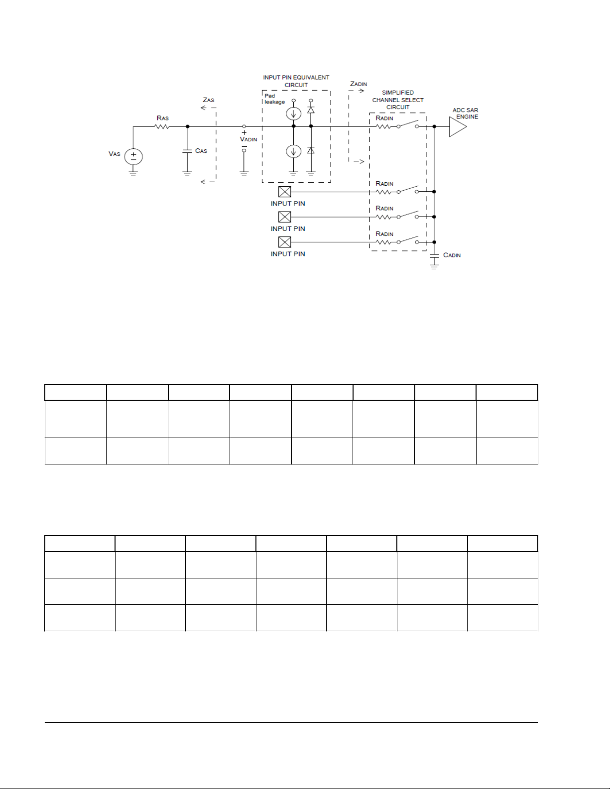
External memory interface
Figure 21. ADC input impedance
1.6.2 Temperature sensor
Table 30. Temperature sensor static and dynamic characteristics
(VDDA_BIAS = 3.3 V, All other supplies = 1.8 V)
Symbol Parameter Conditions Notes Min Typ Max Unit
DT
sen
E
L
1. Absolute temperature accuracy. Based on characterization. Not tested in production
Table 31. Temperature sensor Linear-Least-Square (LLS) fit parameters
Fit parameter Conditions Notes Min Typ Max Unit
LLS slope T
LLS intercept at
0° C
LLS intercept at
25 °C
sensor
temperature
accuracy
linearity error Tamb = -20
T
= -20 °C
amb
to 70 °C
°C to 70 °C
1 - - 2.77 °C
- - 2.79 °C
(VDDA_BIAS = 3.3 V, All other supplies = 1.8 V)
= -20 °C to
amb
70 °C
Tamb = -20 °C
to 70 °C
Tamb = -20 °C
to 70 °C
1, 2 - -1.5738 - mV/°C
1, 2 - 809.55 - mV
1, 2 - 770.4 - mV
1. Based on characterization, Not tested in production.
2. Equation: Temp = 25 - ((Vtemp -Vtemp25)/m) Where: VTEMP is the voltage of the temperature sensor channel at the
ambient temperature VTEMP is the voltage of the temperature sensor channel at 25°C and VDD = 1.8 V m is the voltage
versus temperature slope in V/°C.
42
NXP Semiconductors
i.MX RT500 Low-Power Crossover Processor, Rev. 0, 02/2021
Page 43
Fig 29. Average Vo @ 1.8V supply
500
550
600
650
700
750
800
850
900
‐20 0 20 40 60 80
Vo (mV)
Temperature (C)
Average Vo @ 1.8V supply
Figure 22. Average Vo @ 1.8V supply
External memory interface
1.6.3 Comparator characteristics
T
= -20 C to +70 C; VDD = 1.8 V to 3.6 V.
amb
Symbol Parameter Conditions Notes Min. Typ.
Voffset offset voltage VIC = 0.1 V; VDD =
t
PD
i.MX RT500 Low-Power Crossover Processor, Rev. 0, 02/2021
propagation
delay
Table 32. Comparator characteristics
1.8 V
VIC = 0.9 V; VDD =
1.8 V
VIC = 1.7 V; VDD =
1.8 V
HIGH to LOW; V
= 1.8 V; T
°C VIC = 0.1 V; 100
mV overdrive input
VIC = 0.1 V; rail-torail input
VIC = 0.9 V; 100 mV
overdrive input
VIC = 0.9 V; rail-torail input
Static characteristics
— 6 — mV
— 7 — mV
— 9 — mV
Dynamic characteristics
2 — 2 — μs
DD
= 25
amb
— 915 — ns
2 — 525 — ns
— 600 — ns
Table continues on the next page...
1
Max. Unit
43
NXP Semiconductors
Page 44

External memory interface
Table 32. Comparator characteristics (continued)
Symbol Parameter Conditions Notes Min. Typ.
VIC = 1.7 V; 100 mV
overdrive input
VIC = 1.7 V; rail-torail input
t
PD
propagation
delay
HIGH to LOW; V
= 1.8 V; T
amb
= 25
°C VIC = 0.1 V; 100
mV overdrive input
VIC = 0.1 V; rail-torail input
VIC = 0.9 V; 100 mV
overdrive input
VIC = 0.9 V; rail-torail input
VIC = 1.7 V; 100 mV
overdrive input
VIC = 1.7 V; rail-torail input
t
PD
propagation
delay
LOW to HIGH;
VVDD = 1.8 V; T
= 25 °C, VIC = 0.1
V; 100 mV
overdrive input
VIC = 0.1 V; rail-torail input
VIC = 0.9 V; 100 mV
overdrive input
VIC = 0.9 V; rail-torail input
VIC = 1.7 V; 100 mV
overdrive input
VIC = 1.7 V; rail-torail input
t
PD
propagation
delay
LOW to HIGH;
VVDD = 1.8 V; T
= 25 °C, VIC = 0.1
V; 100 mV
overdrive input
VIC = 0.1 V; rail-torail input
VIC = 0.9 V; 100 mV
overdrive input
VIC = 0.9 V; rail-torail input
VIC = 1.7 V; 100 mV
overdrive input
2 — 500 — ns
— 350 — ns
2 — 270 — ns
DD
— 310 — ns
2 — 340 — ns
— 210 — ns
2 — 150 — ns
— 125 — ns
— 5.8 — μs
amb
— 470 — ns
2 — 750 — ns
— 600 — ns
2 — 5.5 — μs
— 1.25 — μs
— 105 — ns
amb
— 115 — ns
2 — 110 — ns
— 120 — ns
2 — 110 — ns
1
Max. Unit
44
NXP Semiconductors
Table continues on the next page...
i.MX RT500 Low-Power Crossover Processor, Rev. 0, 02/2021
Page 45

External memory interface
Table 32. Comparator characteristics (continued)
Symbol Parameter Conditions Notes Min. Typ.
VIC = 1.7 V; rail-torail input
V
hys
1. Characterized on typical samples, not tested in production
2. 100 mV overdrive corresponds to a square wave from 50 mV below the reference (VIC) to 50 mV above the reference.
3. Input hysteresis is relative to the reference input channel and is software programmable.
hysteresis
3
voltage
HYSTCRT[1:0] =
01
HYSTCRT[1:0] =
10
HYSTCRT[1:0] =
11
— — 13 mV
— 120 — ns
— 27 — mV
— 35 — mV
1
Max. Unit
1.7 Communication interfaces
1.7.1 USART interface
Excluding delays introduced by external device and PCB, the maximum supported bit
rate for USART master synchronous mode is 20 Mbit/s, and the maximum supported
bit rate for USART slave synchronous mode is 20.0 Mbit/s.
The actual USART bit rate depends on the delays introduced by the external trace, the
external device, system clock (HCLK), and capacitive loading.
T
= -20 °C to 70 °C; VDD = 1.71 V to 1.89 V; CL = 20 pF balanced loading on all pins; Input slew = 1 ns, SLEW setting
amb
= standard mode for all pins; Parameters sampled at the 50 % level of the rising or falling edge.
Table 33. USART interface characteristics1
Symbol Parameter Conditions Min. Typ. Max. Unit
USART master (in synchronous mode)
t
su(D)
t
h(D)
t
v(Q)
t
su(D)
t
h(D)
data input setup time
data input hold
time
data output
valid time
data input setup time
data input hold
time
- 0.087 - - ns
- 0.03 - - ns
- 14.058 - 16.412 ns
USART slave (in synchronous mode)
- 0.087 - - ns
- 0.03 - - ns
Table continues on the next page...
i.MX RT500 Low-Power Crossover Processor, Rev. 0, 02/2021
45
NXP Semiconductors
Page 46

TXD
RXD
T
cy(clk)
t
su(D)th(D)
t
v(Q)
START BIT0
t
vQ)
Un_SCLK (CLKPOL = 1)
START
BIT0
BIT1
BIT1
aaa-015074
External memory interface
Table 33. USART interface characteristics1 (continued)
Symbol Parameter Conditions Min. Typ. Max. Unit
t
v(Q)
1. Based on simulation; not tested in production
data output
valid time
- 0 - 3.684 ns
Figure 23. USART timing
1.7.2
T
amb
I2C-bus
= -20 °C to +70 °C; 1.71 V ≤ V
2
Table 34. I
C-bus pins1
≤ 1.89 V.
DD
Symbol Parameter Notes Conditions Min. Max. Unit
f
SCL
SCL clock
frequency
Standard-mode 0 100 kHz
Fast-mode 0 400 kHz
Fast-mode Plus 0 1 MHz
t
f
fall time 2, 3, 4, 5 Both SDA and
SCL signals
Standard-mode
Fast-mode 20x(VDD/3.6V) 300 ns
Fast-mode Plus - 120 ns
t
LOW
t
HIGH
LOW period of
the SCL clock
HIGH period of
the SCL clock
6 Standard-mode 4.7 - μs
Fast-mode 1.3 - μs
Fast-mode Plus 0.5 - μs
6 Standard-mode 4 - μs
Fast-mode 0.6 - μs
1
- 300 ns
1. Parameters are valid over operating temperature range unless otherwise specified. See the I2C-bus specification
UM10204 for details.
46
NXP Semiconductors
Table continues on the next page...
i.MX RT500 Low-Power Crossover Processor, Rev. 0, 02/2021
Page 47

t
f
70 %
30 %
t
f
70 %
30 %
S
70 %
30 %
70 %
30 %
t
HD;DAT
SCL
1 / f
SCL
70 %
30 %
70 %
30 %
t
VD;DAT
t
HIGH
t
LOW
t
SU;DAT
External memory interface
Table 34. I2C-bus pins1 (continued)
Symbol Parameter Notes Conditions Min. Max. Unit
Fast-mode Plus 0.26 - μs
t
HD;DAT
t
SU;DAT
1. Guaranteed by design. Not tested in production.
2. A device must internally provide a hold time of at least 300 ns for the SDA signal (with respect to the VIH(min) of the
SCL signal) to bridge the undefined region of the falling edge of SCL.
3. Cb = total capacitance of one bus line in pF. If mixed with Hs-mode devices, faster fall times are allowed.
4. The maximum tf for the SDA and SCL bus lines is specified at 300 ns. The maximum fall time for the SDA output
stage tf is specified at 250 ns. This allows series protection resistors to be connected in between the SDA and the
SCL pins and the SDA/SCL bus lines without exceeding the maximum specified tf.
5. In Fast-mode Plus, fall time is specified the same for both output stage and bus timing. If series resistors are used,
designers should allow for this when considering bus timing.
6. The MSTTIME register allows programming of certain times for the clock (SCL) high and low times. Please see i.MX
RT500 Low-Power Crossover MCU Reference Manual for further details.
7. t
is the data hold time that is measured from the falling edge of SCL; applies to data in transmission and the
HD;DAT
acknowledge.
8. The maximum t
maximum of t
LOW period (t
releases the clock.
9. t
is the data set-up time that is measured with respect to the rising edge of SCL; applies to data in transmission
SU;DAT
and the acknowledge.
10. A Fast-mode I2C-bus device can be used in a Standard-mode I2C-bus system but the requirement t
must then be met. This will automatically be the case if the device does not stretch the LOW period of the SCL signal.
If such a device does stretch the LOW period of the SCL signal, it must output the next data bit to the SDA line
tr(max) + t
is released. Also the acknowledge timing must meet this set-up time.
data hold time 7, 2, 8 Standard-mode 0 - μs
Fast-mode 0 - μs
Fast-mode Plus 0 - μs
data set-up time 9, 10 Standard-mode 4.7 - ns
Fast-mode 0.6 - ns
Fast-mode Plus 0.26 - ns
could be 3.45 s and 0.9 s for Standard-mode and Fast-mode but must be less than the
HD;DAT
or t
VD;DAT
) of the SCL signal. If the clock stretches the SCL, the data must be valid by the set-up time before it
LOW
= 1000 + 250 = 1250 ns (according to the Standard-mode I2C-bus specification) before the SCL line
SU;DAT
by a transition time. This maximum must only be met if the device does not stretch the
VD;ACK
SU;DAT
= 250 ns
Figure 24. I2C bus pins clock timing
i.MX RT500 Low-Power Crossover Processor, Rev. 0, 02/2021
47
NXP Semiconductors
Page 48

External memory interface
1.7.3 I2S-bus interface
T
= -20 °C to 70 °C; VDD = 1.71 V to 1.89 V; CL = 30 pF balanced loading on all pins; Input slew = 1.0 ns, SLEW setting =
amb
standard mode for all pins; Parameters sampled at the 50 % level of the rising or falling edge.
Table 35. I2S-bus interface pins1, 2
Symbol Parameter Conditions Notes Min. Typ.
Common to master and slave
t
WH
t
WL
t
v(Q)
t
su(D)
t
h(D)
t
v(Q)
t
su(D)
t
h(D)
pulse width
HIGH
pulse width
LOW
data output
valid time
data input setup time
data input
hold time
data output
valid time
data input setup time
data input
hold time
on pins I2Sx_TX_SCK and I2Sx_RX_SCK
(T
cyc
on pins I2Sx_TX_SCK and I2Sx_RX_SCK
(T
cyc
Master
on pin
5
I2Sx_TX_SD
A
on pin I2Sx_WS
on pin
5 1.3 - - ns
I2Sx_RX_SD
A
on pin
5 2.9 - - ns
I2Sx_RX_SD
A
Slave
on pin
5 13.8 23.6 ns
I2Sx_TX_SD
A
on pin
5 4.7 - - ns
I2Sx_RX_SD
A
on pin
I2Sx_WS
on pin
5 0 - - ns
I2Sx_RX_SD
A
on pin
I2Sx_WS
4
/2) -1 - (T
4
/2) -1 - (T
6.798 - 17.505 ns
5 - 16.055 ns
0.9 - - ns
0 - - ns
3
Max. Unit
/2) +1 ns
cyc
/2) +1 ns
cyc
1. Based on simulation; not tested in production.
2. The Flexcomm Interface function clock frequency should not be above 48 MHz. See the data rates section in the I2S
chapter in the i.MX RT500 Low-Power Crossover MCU Reference Manual (IMXRT500RM) to calculate clock and sample
rates.
3. Typical ratings are not guaranteed.
4. Based on simulation. Not tested in production.
5. Clock Divider register (DIV) = 0x0.
48
i.MX RT500 Low-Power Crossover Processor, Rev. 0, 02/2021
NXP Semiconductors
Page 49
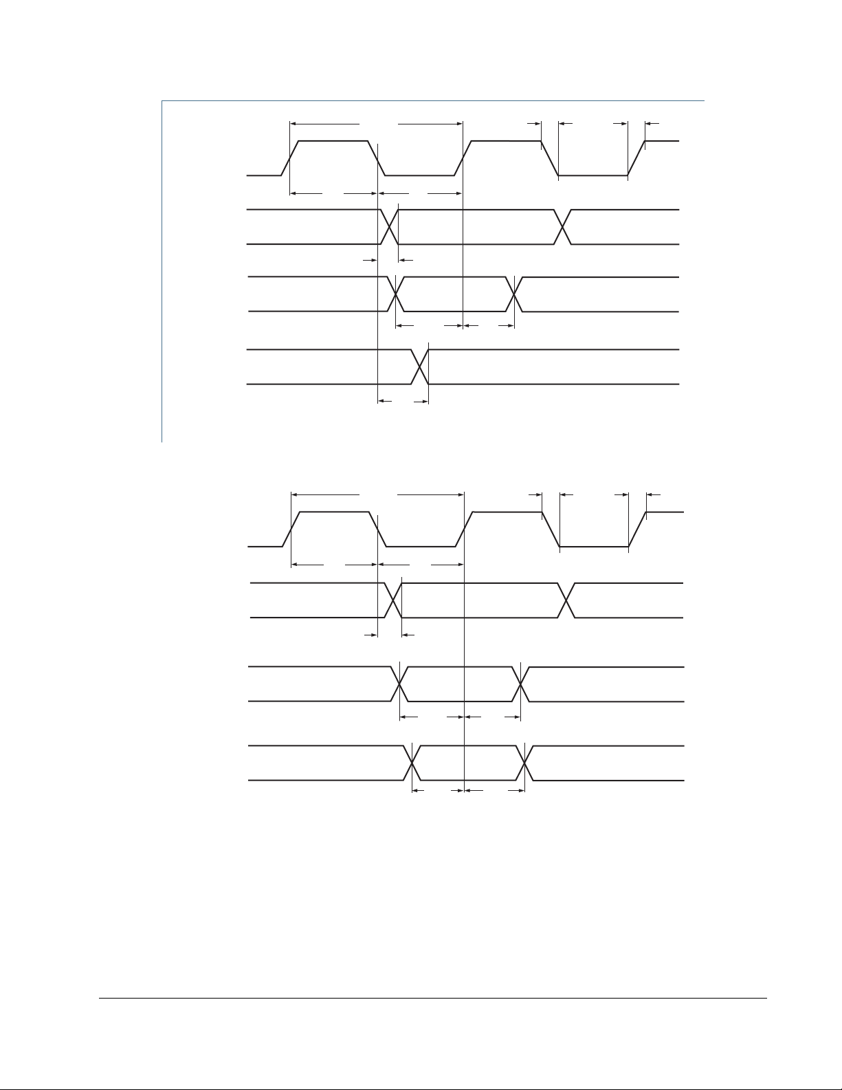
I2Sx_SCK
I2Sx_TX_SDA
I2Sx_WS
T
cy(clk)
t
f
t
r
t
WH
t
WL
t
v(Q)
t
v(Q)
t
su(D)
t
h(D)
I2Sx_RX_SDA
T
cy(clk)
t
f
t
r
t
WH
t
su(D)
t
h(D)
t
su(D)
t
h(D)
t
WL
I2Sx_SCK
I2Sx_WS
I2Sx_TX_SDA
t
v(Q)
External memory interface
Figure 25. I2S-bus timing (master)
Figure 26. I2S-bus timing (slave)
1.7.4
The actual SPI bit rate depends on the delays introduced by the external trace, the
SPI interfaces (Flexcomm interfaces 0-8)
external device, system clock (HCLK), and capacitive loading.
i.MX RT500 Low-Power Crossover Processor, Rev. 0, 02/2021
49
NXP Semiconductors
Page 50

SCK (CPOL = 0)
MOSI (CPHA = 1)
SSEL
MISO (CPHA = 1)
T
cy(clk)
t
DS
t
DH
t
v(Q)
DATA VALID (LSB) DATA VALID
t
v(Q)
SCK (CPOL = 1)
DATA VALID (LSB)
DATA VALID
MOSI (CPHA = 0)
MISO (CPHA = 0)
t
DS
t
DH
DATA VALID (MSB) DATA VALID (MSB)DATA VALID
DATA VALID (LSB)
DATA VALID (LSB)
t
v(Q)
DATA VALID (MSB)
DATA VALID
t
v(Q)
DATA VALID (MSB)
DATA VALID (MSB)
DATA VALID (MSB)
DATA VALID (MSB)
IDLE
IDLE
IDLE
IDLE
DATA VALID (MSB)
External memory interface
Excluding delays introduced by external device and PCB, the maximum supported bit
rate for SPI master mode (transmit/receive) is 25 Mbit/s and the maximum supported
bit rate for SPI slave mode (transmit/receive) is 25 Mbit/s.
T
= -20 °C to 70 °C; 1.71 V ≤ VDD≤ 1.89 V; CL = 10 pF balanced loading on all pins; Input slew = 1 ns, SLEW setting =
amb
standard mode for all pins;. Parameters sampled at the 50 % level of the rising or falling edge.
Table 36. SPI interfaces1
Symbol Parameter Conditions Min. Typ. Max. Unit
SPI master
t
t
t
t
t
v(Q)
t
v(Q)
data set-up time - 5.0 - - ns
DS
data hold time - 0 - - ns
DH
data output valid time - 0 - 13.0 ns
SPI slave
data set-up time - 5.0 - - ns
DS
data hold time - 0 - - ns
DH
data output valid time - 0 - 13 ns
1. Based on simulation; not tested in production
50
NXP Semiconductors
Figure 27. SPI master timing
i.MX RT500 Low-Power Crossover Processor, Rev. 0, 02/2021
Page 51
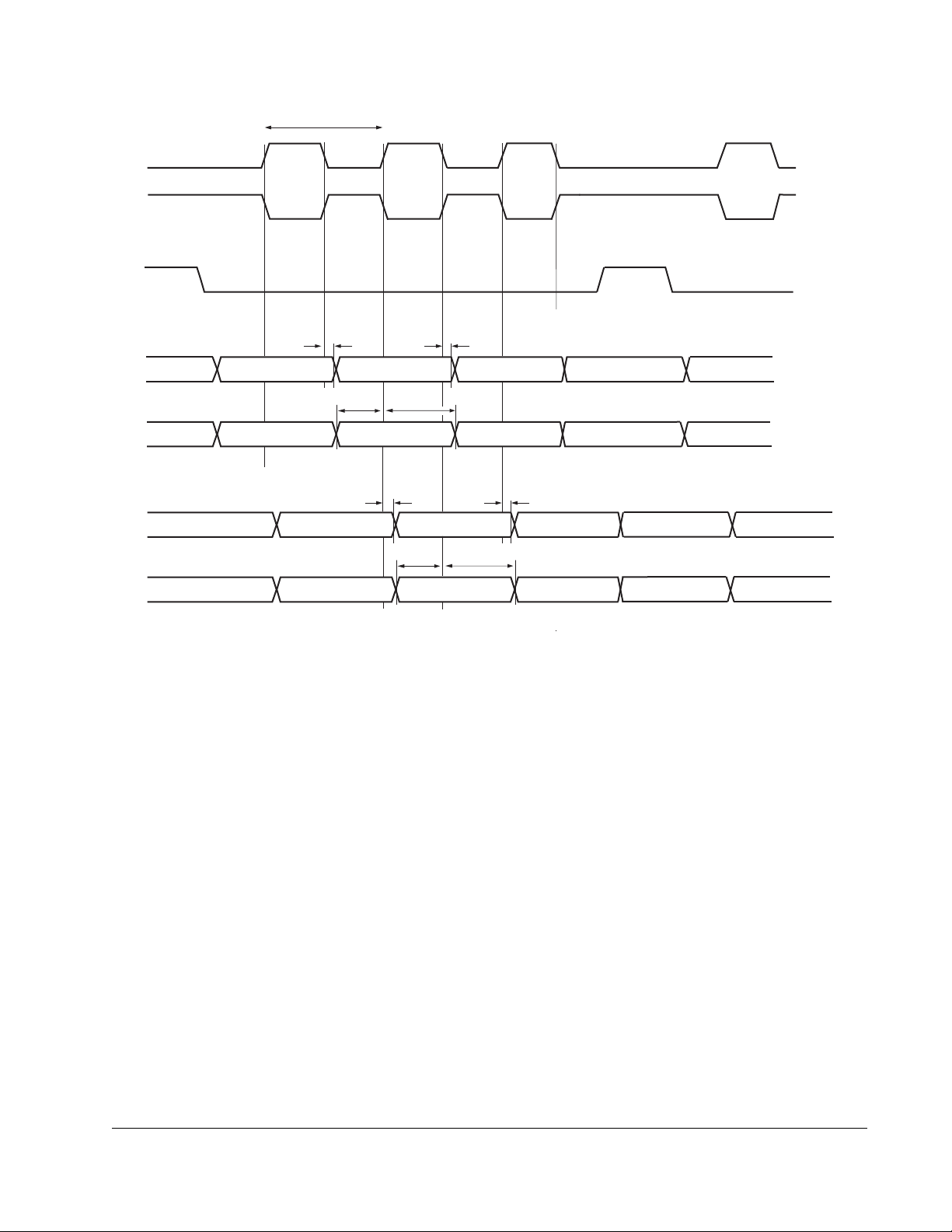
SCK (CPOL = 0)
MISO (CPHA = 1)
SSEL
MOSI (CPHA = 1)
T
cy(clk)
t
DS
t
DH
t
v(Q)
DATA VALID (LSB) DATA VALID
t
v(Q)
SCK (CPOL = 1)
DATA VALID (LSB)
DATA VALID
MISO (CPHA = 0)
MOSI (CPHA = 0)
t
DS
t
DH
DATA VALID (MSB) DATA VALID (MSB)DATA VALID
DATA VALID (LSB)
DATA VALID (LSB)
t
v(Q)
DATA VALID (MSB)
DATA VALID
t
v(Q)
DATA VALID (MSB)
DATA VALID (MSB)
DATA VALID (MSB)
DATA VALID (MSB)
IDLE
IDLE
IDLE
IDLE
DATA VALID (MSB)
External memory interface
Figure 28. SPI slave timing
1.7.5
High-Speed SPI interface (Flexcomm interface 14)
The actual SPI bit rate depends on the delays introduced by the external trace, the
external device, system clock (HCLK), and capacitive loading.
Excluding delays introduced by external device and PCB, the maximum supported bit
rate for SPI master mode (transmit/receive) is 50 Mbit/s.
Excluding delays introduced by external device and PCB, the maximum supported bit
rate for SPI slave mode (receive) is 50 Mbit/s and for SPI slave mode (transmit) is 35
Mbit/s.
T
= -20 °C to 70 °C; 1.71 V ≤ VDD≤ 1.89 V; CL = 10 pF balanced loading on all pins; Input slew = 1 ns, SLEW setting =
amb
standard mode for all pins;. Parameters sampled at the 50 % level of the rising or falling edge.
i.MX RT500 Low-Power Crossover Processor, Rev. 0, 02/2021
NXP Semiconductors
51
Page 52

SCK (CPOL = 0)
MOSI (CPHA = 1)
SSEL
MISO (CPHA = 1)
T
cy(clk)
t
DS
t
DH
t
v(Q)
DATA VALID (LSB) DATA VALID
t
v(Q)
SCK (CPOL = 1)
DATA VALID (LSB)
DATA VALID
MOSI (CPHA = 0)
MISO (CPHA = 0)
t
DS
t
DH
DATA VALID (MSB) DATA VALID (MSB)DATA VALID
DATA VALID (LSB)
DATA VALID (LSB)
t
v(Q)
DATA VALID (MSB)
DATA VALID
t
v(Q)
DATA VALID (MSB)
DATA VALID (MSB)
DATA VALID (MSB)
DATA VALID (MSB)
IDLE
IDLE
IDLE
IDLE
DATA VALID (MSB)
External memory interface
Table 37. High-Speed SPI interfaces1
Symbol Parameter Conditions Min. Typ. Max. Unit
SPI master
t
t
t
v(Q)
t
t
t
v(Q)
1. Based on simulation; not tested in production
data set-up time - 4.0 - - ns
DS
data hold time - 0 - - ns
DH
data output valid time - 0 - 6.0 ns
SPI slave
data set-up time - 3.0 - - ns
DS
data hold time - 0 - - ns
DH
data output valid time - 0 - 10.0 ns
52
NXP Semiconductors
Figure 29. SPI master timing
i.MX RT500 Low-Power Crossover Processor, Rev. 0, 02/2021
Page 53

SCK (CPOL = 0)
MISO (CPHA = 1)
SSEL
MOSI (CPHA = 1)
T
cy(clk)
t
DS
t
DH
t
v(Q)
DATA VALID (LSB) DATA VALID
t
v(Q)
SCK (CPOL = 1)
DATA VALID (LSB)
DATA VALID
MISO (CPHA = 0)
MOSI (CPHA = 0)
t
DS
t
DH
DATA VALID (MSB) DATA VALID (MSB)DATA VALID
DATA VALID (LSB)
DATA VALID (LSB)
t
v(Q)
DATA VALID (MSB)
DATA VALID
t
v(Q)
DATA VALID (MSB)
DATA VALID (MSB)
DATA VALID (MSB)
DATA VALID (MSB)
IDLE
IDLE
IDLE
IDLE
DATA VALID (MSB)
External memory interface
Figure 30. SPI slave timing
1.7.6
T
amb
SD/MMC and SDIO
= -20 °C to +70 °C, VDD = 1.71 V to 1.89 V; VDDCORE = 1.13 V; CL = 10 pF. DLL_CTRL = 0x200, Full Drive Mode
on all pins, Input slew = 1 ns, SLEW setting = standard mode for all pins;. Parameters sampled at the 50 % level of the
rising or falling edge. Based on simulation, not tested in production.
Table 38. SD/MMC and SDIO characteristics (Default Speed (DS), High Speed (HS) SDR-12
and SDR-25)
Symbol Parameter Conditions Min. Typ. Max. Unit
f
clk
f
clk
i.MX RT500 Low-Power Crossover Processor, Rev. 0, 02/2021
clock frequency on pin SD_CLK;
data transfer
mode. DS/
SDR-12 (12.5
MB/s)
clock frequency on pin SD_CLK;
data transfer
mode, HS/
SDR-25 (25
MB/s)
- - 12.5 MHz
- - 25 MHz
Table continues on the next page...
53
NXP Semiconductors
Page 54

External memory interface
Table 38. SD/MMC and SDIO characteristics (Default Speed (DS), High Speed (HS) SDR-12
and SDR-25) (continued)
Symbol Parameter Conditions Min. Typ. Max. Unit
t
su(D)
t
h(D)
t
v(Q)
data input setup time
data input hold
time
data output
valid time
on pins
SD_DATn as
inputs
on pins
SD_CMD as
inputs
on pins
SD_DATn as
inputs
on pins
SD_CMD as
inputs
on pins
SD_DATn as
outputs
on pins
SD_CMD as
outputs
7.5 - - ns
7.5 - - ns
1.0 - - ns
1.0 - - ns
- - 7.5 ns
- - 7.5 ns
T
= -20 °C to +70 °C, VDD = 1.71 V to 1.89 V; VDDCORE = 1.13 V; CL = 10 pF. DLL_CTRL = 0x200, Full Drive Mode on
amb
all pins, Input slew = 1 ns, SLEW setting = standard mode for all pins;. Parameters sampled at the 50 % level of the rising or
falling edge. Based on simulation, not tested in production.
Table 39. SD/MMC and SDIO characteristics ((SDR-50, SDR-104, HS-200 (MMC))
Symbol Parameter Conditions Min. Typ. Max. Unit
f
f
f
t
su(D)
clk
clk
clk
clock frequency on pin SD_CLK;
data transfer
mode, SDR-50
(50 MB/s)
clock frequency on pin SD_CLK;
data transfer
mode, SDR-104
(104 MB/s)
clock frequency on pin SD_CLK;
data transfer
mode, HS-200
(MMC) (200
MB/s)
data input setup time
on pins
SD_DATn as
inputs
on pins
SD_CMD as
inputs
- - 100 MHz
- - 200 MHz
- - 200 MHz
7.5 - - ns
7.5 - - ns
54
NXP Semiconductors
Table continues on the next page...
i.MX RT500 Low-Power Crossover Processor, Rev. 0, 02/2021
Page 55

External memory interface
Table 39. SD/MMC and SDIO characteristics ((SDR-50, SDR-104, HS-200 (MMC)) (continued)
Symbol Parameter Conditions Min. Typ. Max. Unit
t
h(D)
data input hold
time
on pins
SD_DATn as
0 - - ns
inputs
on pins
0 - - ns
SD_CMD as
inputs
t
v(Q)
data output valid
time
on pins
SD_DATn as
0 - 7.5 ns
outputs
on pins
0 - 7.5 ns
SD_CMD as
outputs
T
= -20 °C to +70 °C, VDD = 1.71 V to 1.89 V; VDDCORE = 1.13 V; CL = 10 pF. DLL_CTRL = 0x200, Full Drive Mode
amb
on all pins, Input slew = 1 ns, SLEW setting = standard mode for all pins;. Parameters sampled at the 50 % level of the
rising or falling edge. Based on simulation, not tested in production. HS-400 supported on SD port 0 only.
Table 40. SD/MMC and SDIO characteristics ((DDR-50, HS DDR (MMC))
Symbol Parameter Conditions Min. Typ. Max. Unit
f
clk
clock frequency on pin SD_CLK;
- - 50 MHz
data transfer
mode, DDR-50
(50 MB/s)
f
clk
clock frequency on pin SD_CLK;
52 MHz
data transfer
mode, HS-DDR
(104 MB/s)
t
su(D)
data input setup time
on pins
SD_DATn as
4.8 - - ns
inputs
on pins
4.8 - - ns
SD_CMD as
inputs
t
h(D)
data input hold
time
on pins
SD_DATn as
0 - - ns
inputs
on pins
0 - - ns
SD_CMD as
inputs
t
v(Q)
data output
valid time
on pins
SD_DATn as
0 - 5.0 ns
outputs
on pins
0 - 5.0 ns
SD_CMD as
outputs
i.MX RT500 Low-Power Crossover Processor, Rev. 0, 02/2021
55
NXP Semiconductors
Page 56

SD_CLK
SD_DATn (I)
t
d(QV)
t
h(D)
t
su(D)
T
cy(clk)
t
h(Q)
SD_CMD (O)
SD_CMD (I)
External memory interface
T
= -20 °C to +70 °C, VDD = 1.71 V to 1.89 V; VDDCORE = 1.13 V; CL = 10 pF. DLL_CTRL = 0x200, Full Drive Mode on
amb
all pins, Input slew = 1 ns, SLEW setting = standard mode for all pins;. Parameters sampled at the 50 % level of the rising or
falling edge. Based on simulation, not tested in production. HS-400 supported on SD port 0 only.
Table 41. SD/MMC and SDIO characteristics (HS-400(MMC))
Symbol Parameter Conditions Min. Typ. Max. Unit
f
t
su(D)
t
h(D)
t
v(Q)
clk
clock frequency on pin SD_CLK;
data transfer
mode, HS-400
(400 MB/s)
data input setup time
on pins
SD_DATn as
inputs
on pins
SD_CMD as
inputs
data input hold
time
on pins
SD_DATn as
inputs
on pins
SD_CMD as
inputs
data output valid
time
on pins
SD_DATn as
outputs
on pins
SD_CMD as
outputs
- - 200 MHz
0.5 - - ns
0.5 - - ns
0 - - ns
0 - - ns
0 - 1.0 ns
0 - 1.0 ns
56
NXP Semiconductors
Figure 31. SD/MMC and SDIO timing
i.MX RT500 Low-Power Crossover Processor, Rev. 0, 02/2021
Page 57
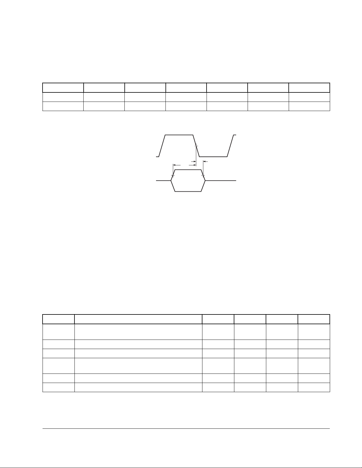
DATA
t
SU
t
DH
External memory interface
1.7.7 DMIC subsystem
T
= -20 °C to 70 °C; VDD = 2.7 V to 3.6 V; CL = 20 pF balanced loading on all pins; Input slew = 1 ns, SLEW set to
amb
standard mode for all pins; Bypass bit = 0; Parameters sampled at the 50% level of the rising or falling edge.
Table 42. Dynamic characteristics1
Symbol Parameter Conditions Min. Typ. Max. Unit
t
DS
t
DH
1. Based on simulated values.
data set-up time - 13 - - ns
data hold time - 0 - - ns
Figure 32. DMIC timing diagram
1.7.8
USB interface characteristics
This section describes the USB1 port High Speed/Full Speed (HS/FS) transceiver. The
USB HS/FS meets the electrical compliance requirements defined in the Universal
Serial Bus Revision 2.0 Specification.
1.7.9
Symbol Description Min. Typ. Max. Unit
V
DP_SRC
V
DM_SRC
V
I
DP_SRC
I
DM_SINK
I
DP_SINK
R
DM_DWN
V
DAT_REF
USB DCD electrical specifications
Table 43. USB DCD electrical specifications
,
USB_DP and USB_DM source voltages (up to 250
μA)
LGC
Threshold voltage for logic high 0.8 — 2.0 V
USB_DP source current 7 10 13 μA
,
USB_DM and USB_DP sink currents 50 100 150 μA
D- pulldown resistance for data pin contact detect 14.25 — 24.8 kΩ
Data detect voltage 0.25 0.33 0.4 V
0.5 — 0.7 V
i.MX RT500 Low-Power Crossover Processor, Rev. 0, 02/2021
57
NXP Semiconductors
Page 58
External memory interface
1.7.10 USB High Speed Transceiver and PHY specifications
This section describes the High Speed USB PHY parameters. The high speed PHY is
capable of full speed signaling as well.
The USB PHY meets the electrical compliance requirements defined in the Universal
Serial Bus Revision 2.0 Specification with the amendments below.
• USB ENGINEERING CHANGE NOTICE
• Title: 5V Short Circuit Withstand Requirement Change
• Applies to: Universal Serial Bus Specification, Revision 2.0
• Errata for USB Revision 2.0 April 27, 2000 as of 12/7/2000
• USB ENGINEERING CHANGE NOTICE
• Title: Pull-up/Pull-down resistors
• Applies to: Universal Serial Bus Specification, Revision 2.0
• USB ENGINEERING CHANGE NOTICE
• Title: Suspend Current Limit Changes
• Applies to: Universal Serial Bus Specification, Revision 2.0
• On-The-Go and Embedded Host Supplement to the USB Revision 2.0 Specification
• Revision 2.0 plus errata and ecn June 4, 2010
• Battery Charging Specification (available from USB-IF)
• Revision 1.2, December 7, 2010
USB0_VBUS pin is a detector function which is 5v tolerant and complies with the
above specifications without needing any external voltage division components.
1.7.11
Improved Inter-Integrated Circuit Interface (MIPI-I3C) specifications
Unless otherwise specified, MIPI-I3C specifications are timed to/from the VIH and/or
VIL signal points.
2
Table 44. MIPI-I3C specifications when communicating with legacy I
Symbol Characteristic 400 kHz/Fast mode 1 MHz/ Fast+ mode Unit
Min. Max. Min. Max.
f
SCL
t
SU_STA
Hold time
(repeated)
58
NXP Semiconductors
SCL Clock Frequency 0 0.4 0 1 MHz
Set-up time for a repeated START condition 600 — 260 — ns
tHD; STA 600 — 260 — ns
Table continues on the next page...
i.MX RT500 Low-Power Crossover Processor, Rev. 0, 02/2021
C devices
Page 59

External memory interface
Table 44. MIPI-I3C specifications when communicating with legacy I2C devices (continued)
Symbol Characteristic 400 kHz/Fast mode 1 MHz/ Fast+ mode Unit
Min. Max. Min. Max.
START
condition
t
LOW
t
HIGH
t
SU_DAT
t
HD_DAT
t
SU_STO
t
BUF
t
SP
LOW period of the SCL clock 1300 — 500 — ns
HIGH period of the SCL clock 600 — 260 — ns
Data set-up time 100 — 50 — ns
Data hold time for I2C bus devices — — — — ns
t
Fall time of SDA and SCL signals 20*(Vdd/5.5v)300 20*(Vdd/5.
f
5 v)
t
Rise time of SDA and SCL signals 20 300 — 120 ns
r
Set-up time for STOP condition 600 — 260 — ns
Bus free time between STOP and START
1.3 — 0.5 — µs
condition
Pulse width of spikes that must be suppressed
0 50 0 50 ns
by the input filter
120 ns
Table 45. MIPI-I3C open drain mode specifications
Symbol Characteristic Min. Max. Unit Notes
t
LOW_OD
t
DIG_OD_LtLOW_OD
t
HIGH
t
fDA_OD
t
SU_OD
t
CAS
t
CBP
t
MMOverlap
t
AVAL
t
IDLE
t
MMLock
1. Cb = total capacitance of the one bus line in pF.
LOW period of the SCL clock 200 — ns
+ t
(min) — ns
fDA_OD
HIGH period of the SCL clock — 41 ns
Fall time of SDA signal t
CF
12 ns 1
Data set-up time during open drain mode 3 — ns
Clock after START (S) Condition
• ENTAS0
• ENTAS1
• ENTAS2
• ENTAS3
Clock before STOP (P) condition t
Current master to secondary master overlap time
38.4 n 1 μ
100 μ
2 m
50 m
(min)/2 — ns
CAS
t
DIG_OD_L
— ns
s
s
s
s
during handoff
Bus available condition 1 — μs
Bus idle condition 1 — ms
Time internal where new master not driving SDA low t
AVAL
— μs
i.MX RT500 Low-Power Crossover Processor, Rev. 0, 02/2021
59
NXP Semiconductors
Page 60

SDA
HD; STA
t
HD; DAT
t
LOW
t
SU; DAT
t
HIGH
t
SU; STA
SR
P
S
S
t
HD; STA
t
SP
t
SU; STO
t
BUF
t
f
t
r
t
f
t
r
SCL
External memory interface
Table 46. MIPI-I3C push-pull specifications for SDR and HDR-DDR modes
Symbol Characteristic Min. Typ. Max. Unit Notes
f
SCL
t
LOW
t
DIG_L
t
HIGH_MIXED
t
DIG_H_MIXE
t
HIGH
t
DIG_H
t
SCO
t
CR
t
t
HD_PP
t
SU_PP
t
CASr
t
CBSr
C
SCL Clock Frequency 0.01 12.5 13 MHz
LOW period of the SCL clock 24 — — ns
32 — — ns
HIGH period of the SCL clock for a mixed bus 24 — — ns
32 — 45 ns 1
D
HIGH period of the SCL clock 24 — — ns
32 — — ns
Clock in to data out for a slave — — 12 ns
SCL clock rise time — — 150 * 1 /
fSCL
(capped at
SCL clock fall time — — 150 * 1 /
CF
fSCL
(capped at
SDA signal data hold
• Master mode
• Slave mode
tCR+3 and
tCF+3
—
—
0
SDA signal setup 3 — — ns
Clock after repeated START (Sr) t
Clock before repeated START (Sr) t
(min) — — ns
CAS
CAS
— — ns
(min)/2
Capacitive load per bus line — — 50 pF
b
60)
60)
—
—
ns
ns
ns
1. When communicating with an I3C Device on a mixed Bus, the t
sure that I2C devices do not interpret I3C signaling as valid I2C signaling.
Figure 33. Timing definition for devices on the I2C bus
1.8
60
NXP Semiconductors
Timer modules
DIG_H_MIXED
period must be constrained in order to make
i.MX RT500 Low-Power Crossover Processor, Rev. 0, 02/2021
Page 61

Architectural overview
1.8.1 SCTimer/PWM output timing
T
= -20 °C to 70 °C; 1.71 V ≤ VDD≤ 1.89 V CL = 20 pF. Simulated skew (over process, voltage, and temperature) of
amb
any two SCT fixed-pin output signals; sampled at the 50% level of the rising or falling edge; values guaranteed by design.
Table 47. SCTimer/PWM output dynamic characteristics
Symbol Parameter Conditions Min. Typ. Max. Unit
t
sk(o)
output skew
time
- 0 - 2.8 ns
2 Architectural overview
The Arm Cortex-M33 includes two AHB-Lite buses: the code bus and the system bus.
The i.MX RT500 uses a multi-layer AHB matrix to connect the Arm Cortex-M33
buses and other bus masters to peripherals in a flexible manner that optimizes
performance by allowing peripherals that are on different slave ports of the matrix to
be accessed simultaneously by different bus masters.
2.1
Detailed block diagram
The following figure shows the detailed block diagram for i. MX RT500
i.MX RT500 Low-Power Crossover Processor, Rev. 0, 02/2021
61
NXP Semiconductors
Page 62
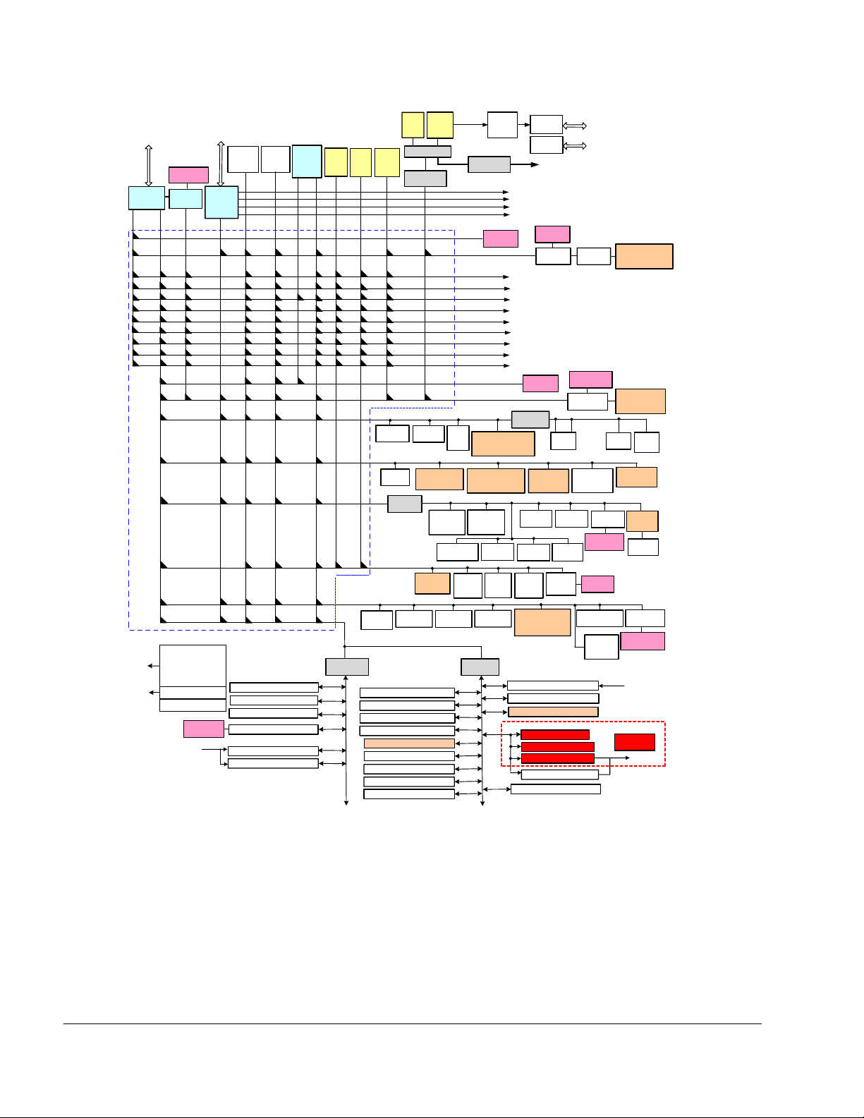
Architectural overview
ISP & Debug
Access Ports
PwrQuad
(
& Casper
PwrQuad
rams
with
processors
MPU
System
M1
Multilayer
AHB Matrix
clock generation,
PLLs, power
control, and
system functions
voltage regulators
RBB
WDT Osc
4
co -
Quad
other
/
PUF Ram
M
33
FPU/
Code
M0
clocks
and
controls
internal
power
Note:
- Orange shaded blocks support General Purpose DMA.
- Yellow shaded blocks include dedicated DMA Ctrl.
ISP & Debug
Access Ports
General
Purpose
)
x
2
kB
Tensilica
Fusion
DSP
Pwr
M2
M3
(intended for M33 - only)
FBB
2KB
General
Smart
Purpose
DMA
DMA
1
DMA
0
Inst
M4
M5
APB slave group0
RSTCTLa, CLKCTLa, SYSCTLa
PVT
I/O Configuration
PUF
Windowed WDT0
MicroTick Timer
DSI
LCDIF
GPU
/
SDIO
SDIO
eMMC
eMMC
Data
M9
M8
M6
M7
P18
P13
registers
AHB to
APB bridge
0,1, 2
3
4
Periph Input Mux Selects
6
14
15
AXI Switch
-
HASH
/
P14
P15
P16
CRYPT
DMA
registers
CRC
Engine
M10
0
AIPS
bridge
S0
:
AHB
AXI
bridge
DMA
registers
Audio Subsys
-
(8
ch D
Decimator
Lite
1
M11
+
P17
SCTimer
PWM
AXI Switch
LCDIF
registers
RSTCTLb, CLKCTLb, SYSCTLb
GPIO interrupt Control
Smart DMA Controller
5x32-bit Timers (T0 - 4)
-Rate Timer
Multi
FlexIO Regs
S1-9
0
1
GPIO
,
-Mic
, etc)
FlexSPI
OTFAD
registers
Random
Number Gen
/
Secure
GPIO 0
Cache Ctrl0 Regs
Cache Ctrl1 Regs
I-ram
-
D
I-ram
D
P0
P1
P2
P3
P4
P5
P6
P7
P8
P9
P10
P11
P12
HS
-7
0
0
Secure
Control
registers
APB bridge
0,1,2
ram
-
ram
-
AHB to
8-12
bridges
-
- SPIs 0-3 - I2Cs 0-3
UARTs 4-7
SPIs 4-7 - I2Cs 4-7
FlexSPI1
registers
5
13
18
19
20
Host
Interface
: AHB
AXI
TCM Bus
0
0
1
1
Boot Rom
192
Flexcoms 0-3
UARTs 0-3 - I2Cs 0-3
Flexcoms 4
-
USB PHY
registers
HS USB
host
registers
PwrQuad
registers
14
15
22-23
6
7
16
17
MIPI
PHY
HS USB
PHY
1-9
To Shared SRAM partitions 0 - 31
MIPI DSI Interface
HS USB Bus
To Shared SRAM partitions 0 - 27
To Shared SRAM partitions 28 - 31
32
KB
cache ram
KB
Cache
Controller
OTFAD
FlexSPI0
Flash Interface
To Shared SRAM partitions 0,1 (32 KB each)
To Shared SRAM partitions 2,3 (32 KB each)
To Shared SRAM partitions 4-7 (32 KB each)
To Shared SRAM partitions 8-11 (64 KB each)
To Shared SRAM partitions 12-15 (128 KB each)
To Shared SRAM partitions 16-19 (256 KB each)
To Shared SRAM partitions 20-23 (256 KB each)
To Shared SRAM partitions 24-27 (256 KB each)
To Shared SRAM partitions 28-31 (256 KB each)
Smart DMA
RAM 32KB
AIPS-Lite
bridge
0
-
7
Flexcom
SPI 14
SDIO0
registers
ACMP
registers
USB Ram
HS USB
device
Interface
registers
Flexcoms8-13
- UARTs8-13
- SPIs8-13
I2Cs8-13 - I2Ss8-13
-
MU0
14
registers
registers
-
I2Cs 4-7
cache ram
Controller
SDIO
PMC
32
KB
Cache
Flexcom15
I2C14
1
controller
16Kb OTP
Array
SRAM
16
-
HASH
slave interface
GPU
registers
SEMA
OTP
KB
CRYPT
FlexSPI
Flash I’face
OS
Timer
Flexcom16
- SPI 15
ADC
-
12
Temp
Sensor
CASPER
registers
CASPER
rams
APB slave group1
Windowed WDT1
WDT Osc
FreqMeasure
I3C0,1
Always-on Power Domain
RTC Alarm Match
RTC Wake Counter
RTC Alarm Counter
32 kHz Osc
& Dividers
RTC Count
RTC Subsec Counter
DSI Phy/Host Controller
1
ch
x
2
2KB
Figure 34. i.MX RT500 detailed block diagram
2.2
Shared system SRAM
The entire system TCM SRAM space (accessed in single cycle) of up to 5 MB is
divided into up to 32 separate partitions, which are accessible to both CPUs, both DMA
engines, and all other AHB bus masters. The Fusion CPU TCMI (Instruction) & TCMD
62
NXP Semiconductors
i.MX RT500 Low-Power Crossover Processor, Rev. 0, 02/2021
Page 63

Architectural overview
(Data) interfaces and the Graphics (GPU/LCD) subsystem each access the RAM via
separate, dedicated 64-bit interfaces. All other masters, including the Cortex-M33
processor and the DMA engines, access RAM via the main 32-bit AHB bus. All of
these accesses are single-cycle with the exception of the GPU/LCD. Hardware
interface modules arbitrate access to each RAM partition between the main AHB bus,
the graphics AHB bus and the Fusion Tightly-Coupled-Memory buses.
Under software control, each of the 32 individual SRAM partitions can be used
exclusively as code or as data, dedicated either CPU, or shared among the various
masters. Each partition can be independently placed in a low-power retention mode or
powered off entirely.
2.3
RT500 modules list
The i.MX RT500 contains a variety of digital and analog modules. The following
table describes briefly about these modules.
Table 48. i.MX RT500 modules list
Block Name Block
Mnemonic
ARM Cortex M33 processor MCU Core module The Arm Cortex-M33 is a general
Table continues on the next page...
Subsystem Brief description
Arm core modules
purpose, 32-bit microprocessor, which
offers high performance and very low
power consumption. The Arm CortexM33 offers many new features, including
a Thumb-2 instruction set, low interrupt
latency, hardware multiply and divide,
interruptable/continuable multiple load
and store instructions, automatic state
save and restore for interrupts, tightly
integrated interrupt controller with wakeup interrupt controller, and multiple core
buses capable of simultaneous
accesses. M33 includes ARM’s
TrustZone M for enhanced security as
well as a co-processor interface. This
interface is used on this device to provide
hardware acceleration for DSP functions
(Powerquad co-processor) and Security/
cryptography operations (CASPER coprocessor). A 3-stage pipeline is
employed so that all parts of the
processing and memory systems can
operate continuously. Typically, while
one instruction is being executed, its
i.MX RT500 Low-Power Crossover Processor, Rev. 0, 02/2021
63
NXP Semiconductors
Page 64

Architectural overview
Table 48. i.MX RT500 modules list (continued)
Block Name Block
Mnemonic
Arm Cortex-M33 integrated
Floating Point Unit (FPU)
Memory Protection Unit MPU Core module The Cortex-M33 includes a Memory
Nested Vectored Interrupt
Controller (NVIC) for CortexM33
System Tick timer (SysTick) SysTick Core modules The Arm Cortex-M33 includes a system
On-Chip static RAM SRAM Memories The i.MX RT500 supports up to 5 MB
FPU Core modules The FPU fully supports single-precision
NVIC Core modules The NVIC is an integral part of the
Table continues on the next page...
Subsystem Brief description
successor is being decoded, and a third
instruction is being fetched from memory.
add, subtract, multiply, divide, multiply
and accumulate, and square root
operations. It also provides conversions
between fixed-point and floating-point
data formats, and floating-point constant
instructions. The FPU provides floatingpoint computation functionality that is
compliant with the ANSI/IEEE Std
754-2008, IEEE Standard for Binary
Floating-Point Arithmetic, referred to as
the IEEE 754 standard.
Protection Unit (MPU) which can be used
to improve the reliability of an embedded
system by protecting critical data within
the user application. The MPU allows
separating processing tasks by
disallowing access to each other's data,
disabling access to memory regions,
allowing memory regions to be defined
as read-only and detecting unexpected
memory accesses that could potentially
break the system. The MPU separates
the memory into distinct regions and
implements protection by preventing
disallowed accesses. The MPU supports
up to eight regions each of which can be
divided into eight subregions. Accesses
to memory locations that are not defined
in the MPU regions, or not permitted by
the region setting, will cause the Memory
Management Fault exception to take
place.
Cortex-M33. The tight coupling to the
CPU allows for low interrupt latency and
efficient processing of late arriving
interrupts.
tick timer (SysTick) that is intended to
generate a dedicated SYSTICK
exception. The clock source for the
SysTick can be the FRO or the CortexM33 core clock.
Memories
SRAM with separate bus master access
64
NXP Semiconductors
i.MX RT500 Low-Power Crossover Processor, Rev. 0, 02/2021
Page 65

Table 48. i.MX RT500 modules list (continued)
Architectural overview
Block Name Block
Mnemonic
On-chip ROM ROM Memories The 192 KB on-chip ROM contains the
One-Time Programmable
memory
192 MHz Free Running
Oscillator (FRO)
1 MHz Low Power Oscillator LPO System Control The 1 MHz oscillator provides an ultra
Crystal Oscillator - System Control The main crystal oscillator on the i.MX
OTP Memories The i.MX RT500 contains up to 16 kbits
FRO System control The 192 MHz FRO oscillator provides a
Table continues on the next page...
Subsystem Brief description
for higher throughput and individual
power control for low-power operation.
boot loader and the following Application
Programming Interfaces (API):
• In-Application Programming (IAP)
and In-System Programming (ISP).
• ROM-based USB drivers (HID,
CDC, MSC). Supports flash
updates via USB.
• Supports booting from valid Octal/
Quad SPI, eMMC, USB, USART,
SPI, and I2C. • Legacy, Single, and
Dual image boot.
• OTP API for programming OTP
memory.
• Random Number Generator (RNG)
API.
one-time-programmable memory used
for part configuration, key storage (as an
alternative to PUF) and other uses.
Clock sources
high-frequency clock source that can be
used without the need for a high-power
PLL for many applications. This oscillator
is factory trimmed to ±1% accuracy but
can optionally be tuned to ±0.1%
accuracy using an accurate, known
reference clock such as the crystal
oscillator. The 192 MHz FRO, or a
divided version of it, may be used as the
main system clock and for many other
purposes.
low-power, low-frequency clock source
that can be used to clock a variety of
functions including the Watchdog Timer
(WWDT) and the OS/EVENT Timer. It
can also be used as the main system
clock for low-power operation. On Reset,
the device boots using this 1 MHz
oscillator.
The 1 MHz Low Power oscillator is
accurate to ±5% over temperature.
RT500 can be used with crystal
frequencies from 4 MHz to 26 MHz. The
i.MX RT500 Low-Power Crossover Processor, Rev. 0, 02/2021
65
NXP Semiconductors
Page 66

Architectural overview
Table 48. i.MX RT500 modules list (continued)
Block Name Block
Mnemonic
32 KHz Crystal Oscillator - System Control The 32KHz oscillator resides in the
System Control (PLLs)
System PLL (PLL0) PLL0 System Control The system PLL accepts an input clock
Audio PLL (PLL1) PLL1 System Control The audio PLL accepts an input clock
General Purpose I/O (GPIO) GPIO Pin Muxing The i.MX RT500 provides up to six GPIO
Pin Interrupt and Pattern
Match (PINT)
- I/O Mux The pin interrupt block configures up to
Table continues on the next page...
Subsystem Brief description
crystal oscillator may be used to drive a
PLL to achieve higher clock rates.
"always-on" domain and is used to drive
the Real Time Clock. It is also available
for use for a variety of other purposes
including low-power UART operation or
as the main system clock for very low
frequency operation
frequency in the range of 32.768 kHz to
25 MHz. The input frequency is multiplied
up to a high frequency with a Current
Controlled Oscillator (CCO). Generates
four independent outputs (PFD0-3).
frequency in the range of 1 MHz to 25
MHz. The input frequency is multiplied up
to a high frequency with a Current
Controlled Oscillator (CCO). The PLL can
be enabled or disabled by software.
I/O Muxing
ports with a total of up to 136 GPIO pins.
Device pins that are not connected to a
specific peripheral function are controlled
by the GPIO registers. Pins may be
dynamically configured as inputs or
outputs. Separate registers allow setting
or clearing any number of outputs
simultaneously. The current level of a
port pin can be read back no matter what
peripheral is selected for that pin. It can
optionally contribute to one of two GPIO
group interrupts, with selection of
polarity, level or edge detection.
eight pins from all digital pins for
providing eight external interrupts
connected to the NVIC. The pattern
match engine can optionally be used in
conjunction with software to create
complex state machines based on pin
inputs. Any digital pin, independent of the
function selected through the switch
matrix can be configured through the
SYSCON block as an input to the pin
interrupt or pattern match engine. The
registers that control the pin interrupt or
66
NXP Semiconductors
i.MX RT500 Low-Power Crossover Processor, Rev. 0, 02/2021
Page 67

Table 48. i.MX RT500 modules list (continued)
Architectural overview
Block Name Block
High-speed USB Host/
Device interface (USB1)
Flex SPI Controller
(FlexSPI)
Subsystem Brief description
Mnemonic
pattern match engine are located on the
I/O+ bus for fast single-cycle access.
Communication peripherals
USB1 Communication interfaces The Universal Serial Bus (USB) is a 4-
wire bus that supports communication
between a host and one or more (up to
127) peripherals. The host controller
allocates the USB bandwidth to attached
devices through a token-based protocol.
The device controller enables 480 Mbit/s
data exchange with a USB host
controller. It consists of a register
interface, serial interface engine,
endpoint buffer memory. The bus
supports hot plugging and dynamic
configuration of the devices. All
transactions are initiated by the host
controller.
FlexSPI Communication interfaces Two FlexSPI Interface modules,
supporting Octal and Quad SPI memory
devices are provided. The first FlexSPI
instance is primarily intended for code
execution from off-chip SPI flash
memory. The second instance is
primarily intended to access data from
RAMs like HyperRAM or pSRAM
(particularly for graphics). The second
instance is accessible by the DSP
processor as well as the M33. Target will
be for both interfaces to support up to
200 MHz DDR/SDR The FlexSPI
interfaces support HyperFlash,
HyperRAM and Xccela memory types,
among others. The first FlexSPI interface
(FlexSPI0) supports execute-in-place and
on-the-fly decryption using the latest
OTFAD module. It also provides a
mechanism to shift a designated range of
addresses to a different region of off-chip
memory to support dual-image boot. Both
FlexSPI Interfaces include a 32 KB cache
with an CACHE64 AHB-cache controller.
Additional logic is provided at the
CACHE64 interface to enable different
caching policies for different address
regions. These policies include:
• Write-back
• Write-through
• Non-cached
Table continues on the next page...
i.MX RT500 Low-Power Crossover Processor, Rev. 0, 02/2021
.
67
NXP Semiconductors
Page 68

Architectural overview
Table 48. i.MX RT500 modules list (continued)
Block Name Block
Mnemonic
SD/eMMC interfaces uSDHC Communication interfaces Two uSDHC SDIO/MMC card interfaces
Flexcomm Interface FlexComm Communication interfaces Following are the features of FlexComm:
I3C interface
General-purpose 32-bit
timers/external event
counter
SCTimer/PWM
I3C Communication interface Two I3C master/slave interfaces are
Counter/Timer modules
- Counter/Timers The i.MX RT500 includes five general-
SCT/PWM Counters/Timers The SCTimer/PWM allows a wide variety
Table continues on the next page...
Subsystem Brief description
are provided. One instance of this
interface (SDIO0) supports the eMMC
5.0 standard including HS400 DDR
mode. The other instance supports 100
MHz SDR, 50 MHz DDR.
• USART with asynchronous
operation or synchronous master
or slave operation.
• SPI master or slave, with up to 4
slave selects.
• I2C, including separate master,
slave, and monitor functions.
• Two I2S functions using Flexcomm
Interface 6 and Flexcomm Interface
7.
• Data for USART, SPI, and I2S
traffic uses the Flexcomm Interface
FIFO. The I2C function does not
use the FIFO.
provided, both of which support DDR.
purpose 32-bit timer/counters. The timer/
counter is designed to count cycles of the
system derived clock or an externallysupplied clock. It can optionally generate
interrupts, generate timed DMA requests,
or perform other actions at specified
timer values, based on four match
registers. Each timer/counter also
includes two capture inputs to trap the
timer value when an input signal
transitions, optionally generating an
interrupt.
of timing, counting, output modulation,
and input capture operations. The inputs
and outputs of the SCTimer/PWM are
shared with the capture and match
inputs/outputs of the 32-bit generalpurpose counter/timers. The
SCTimer/PWM can be configured as two
16-bit counters or a unified 32-bit
counter. In the two-counter case, in
addition to the counter value the following
operational elements are independent for
each half:
68
NXP Semiconductors
i.MX RT500 Low-Power Crossover Processor, Rev. 0, 02/2021
Page 69

Table 48. i.MX RT500 modules list (continued)
Architectural overview
Block Name Block
Mnemonic
Windowed Watchdog Timer
(WWDT)
Real Time Clock Timer RTC Timer Timers The RTC timer is a 32-bit timer which
Multi-Rate Timer MRT Timers The Multi-Rate Timer (MRT) provides a
OS/Event Timer - Timers An OS/EVENT Timer module provides a
WWDT Timers The purpose of the watchdog is to reset
Subsystem Brief description
• State variable
• Limit, halt, stop, and start
conditions.
• Values of Match/Capture registers,
plus reload or capture control
values.
In the two-counter case, the following
operational elements are global to the
SCTimer/PWM, but the last three can
use match conditions from either counter:
• Clock selection
• Inputs
• Events
• Outputs
• Interrupts
the controller if software fails to
periodically service it within a
programmable time window. A separate
Watchdog Timer is provided for each of
the two CPUs.
counts down from a preset value to zero.
At zero, the preset value is reloaded and
the counter continues. The RTC timer
uses the 32.768 kHz clock input to create
a 1 Hz or 1 kHz clock.
repetitive interrupt timer with four
channels. Each channel can be
programmed with an independent time
interval, and each channel operates
independently from the other channels.
common timebase between the two
CPUs for event synchronization and
timestamping. The OS/EVENT Timer is
comprised of a shared, free-running
counter readable by each CPU and
individual match and capture registers for
each CPU. The shared and local
counters in this module are implemented
using Gray code. This will enable them to
be read asynchronously by the
processing domains. The main counter in
the OS/EVENT Timer module begins
counting immediately following power-up
and continues counting through any
subsequent system resets (except those
caused by a new POR).
Table continues on the next page...
i.MX RT500 Low-Power Crossover Processor, Rev. 0, 02/2021
69
NXP Semiconductors
Page 70

Architectural overview
Table 48. i.MX RT500 modules list (continued)
Block Name Block
Mnemonic
Micro-Tick Timer MTR Timers A 32-bit MicroTick timer that runs from
Graphics Peripherals
2D Graphics Processing
Unit (GPU)
MIPI DSI Controller with onchip PHY
Flexio FlexIO Graphics/Multimedia The Flexio module under "Others"
DMA Controller DMA Other The DMA controller allows peripheral-to
DMIC Subsystem DMIC Other DMIC subsystem includes:
GPU2D Graphics A 2D graphics engine is provided. The
MIPI-DSI Graphics LCD Display Controller, with on-chip MIPI
Other Digital Peripherals
Table continues on the next page...
Subsystem Brief description
the 1 MHz low-power oscillator. This
timer can wake up the device from
reduced power modes up to deep-sleep,
with extremely low power consumption.
The MicroTick timer has an added
timestamp feature in the form of 4
capture registers.
GPU is used to generate graphics data
for display by the LCD Display Controller.
The GPU supports displays up to
640x480.
DSI Phy provides transfer rates up to
895.1 Mbps to support 1024x480
displays with 24-bit color at 60 frames
per second. A parallel DBI interface is
also provided (alternative to the serial
PHY).
category can be used to interface to an
LCD with a parallel interface.
memory, memory-to-peripheral, and
memory-to-memory transactions. Each
DMA stream provides unidirectional DMA
transfers for a single source and
destination. Two identical DMA
controllers are provided on i.MX RT500.
The user may elect to dedicate one of
these to the Cortex M-33 CPU and the
other for use by the DSP CPU and/or one
may be used as a secure DMA the other
non-secure.
• Pulse-Density Modulation (PDM)
data input for left and/or right
channels on 1 or 2 buses.
• Flexible decimation.
• 16 entry FIFO for each channel.
• DC blocking or unaltered DC bias
can be selected.
• Data can be transferred using DMA
from deep-sleep mode without
waking up the CPU, then
70
NXP Semiconductors
i.MX RT500 Low-Power Crossover Processor, Rev. 0, 02/2021
Page 71

Table 48. i.MX RT500 modules list (continued)
Architectural overview
Block Name Block
Mnemonic
Smart DMA Engine Smart DMA
Controller
Flexible Input/Output FlexIO Others The Flexible Input/Output (FlexIO)
Cyclic Redundancy
Check(CRC) engine
12-bit Analog to Digital
Converter
Temperature Sensor - Analog The temperature sensor transducer uses
CRC Other The Cyclic Redundancy Check (CRC)
ADC Analog The ADC supports a resolution of 12-bit
Other Smart DMA Controller with dedicated 32
Subsystem Brief description
automatically returning to deepsleep mode.
• Data can be streamed directly to
I2S on Flexcomm Interface 7.
KB code RAM
module is capable of supporting a wide
range of protocols including, but not
limited to: UART, I2C, SPI, I2S, camera
interface, display interface, PWM
waveform generation, and so on
generator with programmable polynomial
settings supports several CRC standards
commonly used. To save system power
and bus bandwidth, the CRC engine
supports DMA transfers.
Analog Peripherals
and fast conversion rates of up to 1
Msamples/s. Sequences of analog-todigital conversions can be triggered by
multiple sources. Possible trigger
sources are the SCTimer/PWM, external
pins, and the Arm TXEV interrupt.
an intrinsic pn-junction diode reference
and outputs a CTAT voltage
(Complement To Absolute Temperature).
The output voltage varies inversely with
device temperature with an absolute
accuracy of better than ±5 °C over the
full temperature range (-20 °C to +70 °C).
The temperature sensor is only
approximately linear with a slight
curvature. The output voltage is
measured over different ranges of
temperatures and fit with linear-leastsquare lines. After power-up, the
temperature sensor output must be
allowed to settle to its stable value before
it can be used as an accurate ADC input.
For an accurate measurement of the
temperature sensor by the ADC, the ADC
must be configured in single-channel
burst mode. The last value of a nineconversion (or more) burst provides an
accurate result.
Table continues on the next page...
i.MX RT500 Low-Power Crossover Processor, Rev. 0, 02/2021
71
NXP Semiconductors
Page 72

Application information
Table 48. i.MX RT500 modules list (continued)
Block Name Block
Mnemonic
Analog Comparator CMP Analog The Comparator (CMP) module provides
Security Subsystem - Security Comprises of:
On-The-Fly AES Decryption
True Random Number
Generator
OTFAD Security The On-The-Fly AES Decryption
TRNG Security The True Random Number Generator
Subsystem Brief description
a circuit for comparing two analog input
voltages. The comparator circuit is
designed to operate across the full range
of the supply voltage (rail to rail
operation).
Security
• Trust Zone M
• AES256 Decryption Engine.
• SHA-1, SHA-2 HASH Engine.
• Physical Unclonable Function
(PUF) Key Generation
• CASPAR security Cortex-M33 coprocessor
• OTP memory
• Random number generator (RNG)
• On-the-Fly Decryption on FlexSPI
interface
.
(OTFAD) module provides an advanced
hardware implementation that minimizes
any incremental cycles of latency
introduced by the decryption in the
overall external memory access time.
The OTFAD engine also includes
complete hardware support for a
standard AES key unwrap mechanism to
decrypt a key BLOB data instruction
containing the parameters needed for up
to 4 unique AES contexts.
(TRNG) module is used to generate high
quality, cryptographically secure, random
data. The TRNG module is capable of
generating its own entropy using an
integrated ring oscillator.
3 Application information
3.1 Current consumption vs. memory partitions
The following figure shows the current consumption vs memory partitions:
72
NXP Semiconductors
i.MX RT500 Low-Power Crossover Processor, Rev. 0, 02/2021
Page 73
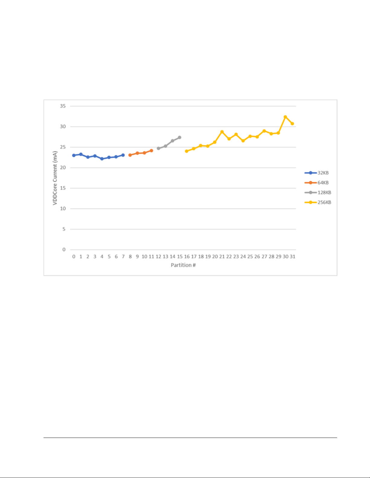
Application information
M33 active, running enhanced-while(1) code in different partitions.
Typical silicon, VDDCore=1.1V, Temperature=25℃, FBB, HCLK=192MHz (FRO).
All memories array/periphery ON (PDRUNCFG2/3) and only one partition clocked
(AHB_SRAM_ACCESS_DISABLE register).
Figure 35. Current consumption vs. memory partitions
3.2
Standard I/O pin configuration
The following figure shows the possible pin modes for standard I/O pins:
The default configuration for standard I/O pins is Z mode. The weak MOS devices
provide a drive capability equivalent to pull-up and pull-down resistors.
i.MX RT500 Low-Power Crossover Processor, Rev. 0, 02/2021
NXP Semiconductors
73
Page 74
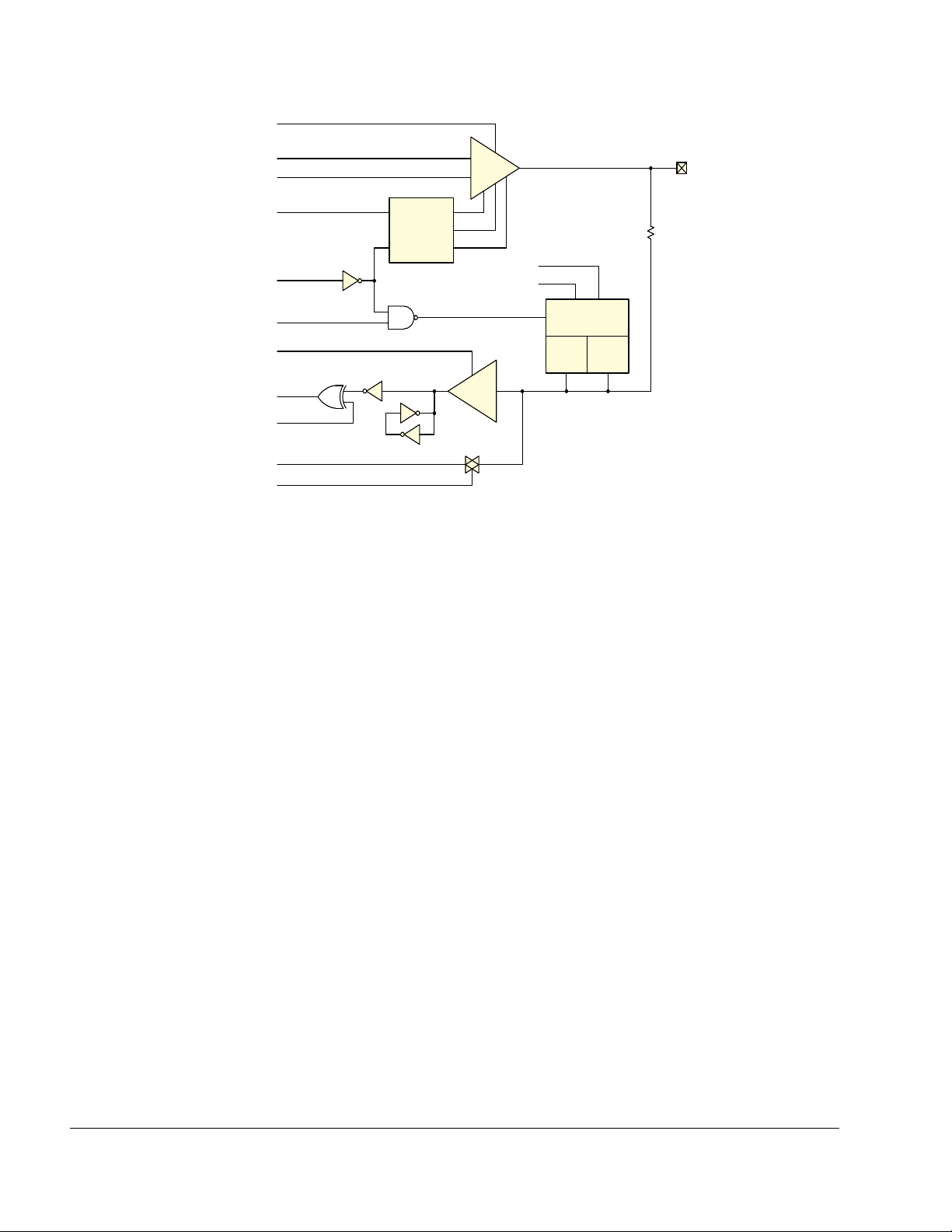
from selected
pin function
driver
configuration
logic
FULLDRIVE
device
pin
ODENA
SLEWRATE
PUPDENA
PUPDSEL
IBENA
IIENA
data out
analog in
data in
output
driver
PUPDENA
PU/PD/keeper
logic
PU/PD
devices
keeper
device
input
receiver
Application information
Figure 36. Pin configuration
3.3
I/O power consumption
I/O pins are contributing to the overall dynamic and static power consumption of the
part. If pins are configured as digital inputs, a static current can flow depending on the
voltage level at the pin and the setting of the internal pull-up and pull-down resistors.
This current can be calculated using the parameters Rpu and Rpd given in Table 6 for a
given input voltage VI. For pins set to output, the current drive strength is given by
parameters IOH and IOL in Table 6, but for calculating the total static current, you also
need to consider any external loads connected to the pin.
I/O pins also contribute to the dynamic power consumption when the pins are switching
because the VDD supply provides the current to charge and discharge all internal and
external capacitive loads connected to the pin in addition to powering the I/O circuitry.
The contribution from the I/O switching current Isw can be calculated as follows for any
given switching frequency fsw if the external capacitive load (C
6 for the internal I/O capacitance):
Isw = VDD x fsw x (Cio + C
ext
) is known (see Table
ext
)
74
NXP Semiconductors
i.MX RT500 Low-Power Crossover Processor, Rev. 0, 02/2021
Page 75
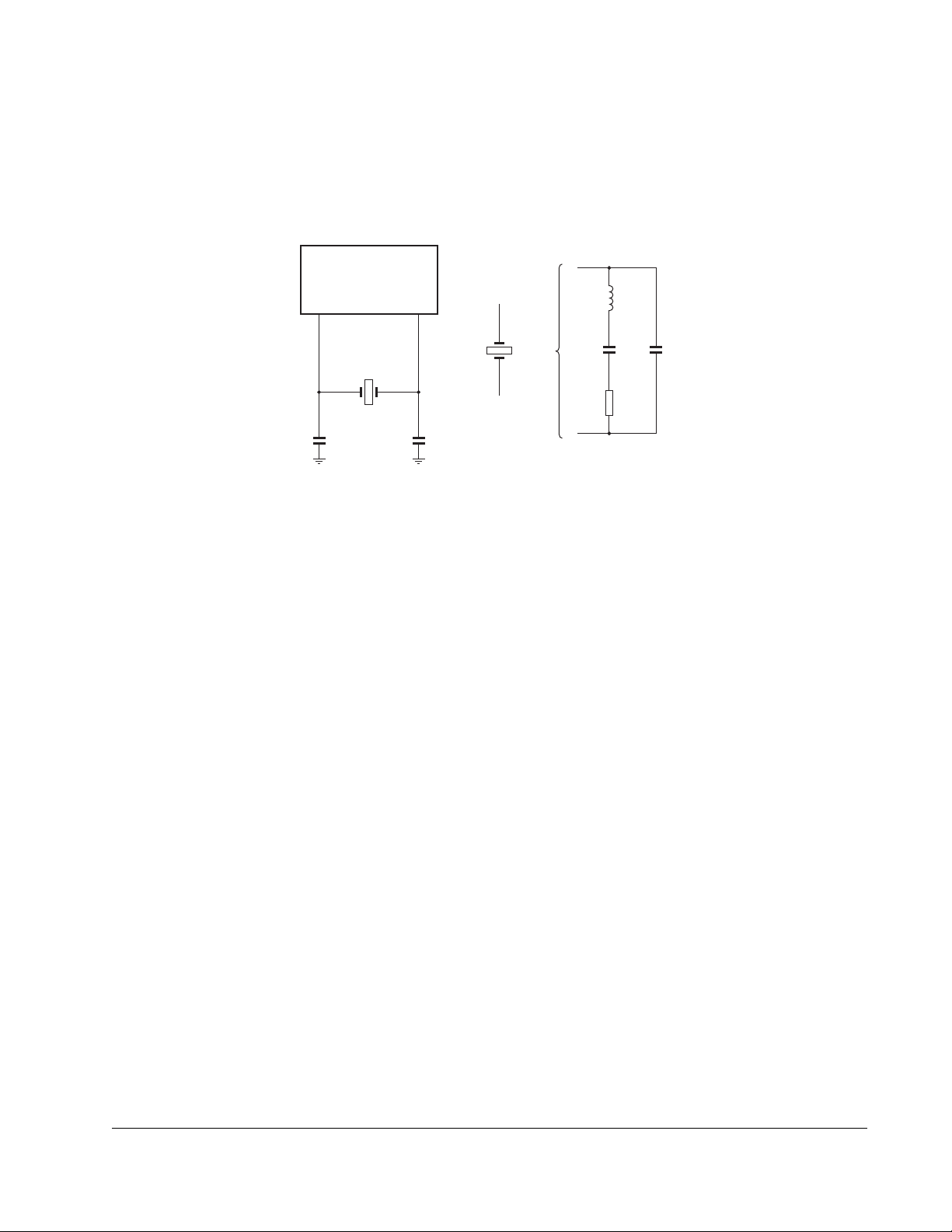
RTxxx
RTCXIN RTCXOUT
C
X2
C
X1
XTAL
=
C
L
C
P
R
S
L
Application information
3.4 RTC oscillator
In the RTC oscillator circuit, only the crystal (XTAL) and the capacitances CX1 and
CX2 need to be connected externally on RTCXIN and RTCXOUT. See the following
figure.
Figure 37. RTC oscillator components
For best results, it is very critical to select a matching crystal for the on-chip oscillator.
Load capacitance (CL), series resistance (RS), and drive level (DL) are important
parameters to consider while choosing the crystal. After selecting the proper crystal,
the external load capacitor CX1 and CX2 values can also be generally determined by
the following expression:
CX1 = C
= 2CL - C
X2
Pad
- 2C
STRAY
Where:
CL - Crystal load capacitance
C
- Pad capacitance of the RTCXIN and RTCXOUT pins (~3 pF, for each pad).
Pad
C
STRAY
– stray capacitance between RTCXIN and RTCXOUT pins.
For example:
CL = 9 pF
CX1 = C
CX1 = C
= 2CL - C
X2
= 2*9 - 3 - 0 = 15 pF
X2
Pad
- 2C
STRAY
Although C
external components influences the optimal values of external load capacitors.
Therefore, it is recommended to fine tune the values of external load capacitors on
i.MX RT500 Low-Power Crossover Processor, Rev. 0, 02/2021
STRAY
can be ignored in general, the actual board layout and placement of
NXP Semiconductors
75
Page 76

Application information
actual hardware board to get the accurate clock frequency. For fine tuning, output the
RTC Clock to the CLOCKOUT pin and optimize the values of external load capacitors
for minimum frequency deviation.
To use bypass mode on RTC, remove the crystal, drive an external clock to RTCIN pin,
and float the RTCOUT pin.
3.4.1 RTC Printed Circuit Board (PCB) design guidelines
• Connect the crystal and external load capacitors on the PCB as close as possible to
the oscillator input and output pins of the chip.
• The length of traces in the oscillation circuit should be as short as possible and must
not cross other signal lines.
• Ensure that the load capacitors CX1, CX2, and CX3, in case of third overtone
crystal usage, have a common ground plane.
• Loops must be made as small as possible to minimize the noise coupled in through
the PCB and to keep the parasitics as small as possible.
• Lay out the ground (GND) pattern under crystal unit.
• Do not lay out other signal lines under crystal unit for multi-layered PCB.
3.5
XTAL oscillator
In the XTAL oscillator circuit, only the crystal (XTAL) and the capacitances CX and C
need to be connected externally on XTALIN and XTALOUT. See the figure below.
Y
76
NXP Semiconductors
i.MX RT500 Low-Power Crossover Processor, Rev. 0, 02/2021
Page 77
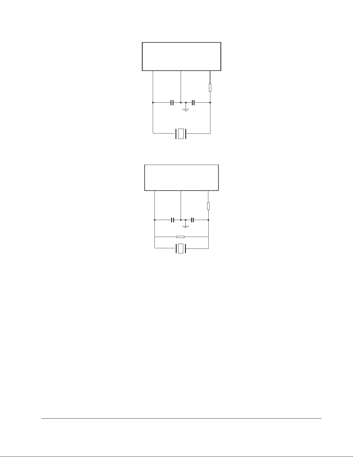
Crystal
C
y
C
x
XTALIN
OSC Module
XTALOUT
V
ss
R
s
Crystal
C
y
C
x
XTALIN
OSC Module
XTALOUT
V
ss
R
s
R
f
Crystal
C
y
C
x
XTALIN
OSC Module
XTALOUT
V
ss
R
s
R
f
Application information
Figure 38. XTAL oscillator connection - Low-Power Mode
Figure 39. XTAL oscillator connection - High Gain Mode
For best results, it is very critical to select a matching crystal for the on-chip oscillator.
Load capacitance (CL), series resistance (RS), and drive level (DL) are important
parameters to consider while choosing the crystal. After selecting the proper crystal,
the external load capacitor CX1 and CX2 values can also be generally determined by
the following expression:
Cx = Cy = 2CL - C
Pad
- 2C
STRAY
Where:
CL - Crystal load capacitance
C
- Pad capacitance of the XTALIN and XTALOUT pins (~3 pF, for each pad).
Pad
C
For example:
i.MX RT500 Low-Power Crossover Processor, Rev. 0, 02/2021
STRAY
– stray capacitance between XTALIN and XTALOUT pins.
NXP Semiconductors
77
Page 78

Application information
CL = 9 pF
Cx = Cy = 2CL - C
Pad
- 2C
STRAY
Cx = Cy = 2*9 - 3 - 0 = 15 pF
Although C
STRAY
can be ignored in general, the actual board layout and placement of
external components influences the optimal values of external load capacitors.
Therefore, it is recommended to fine tune the values of external load capacitors on
actual hardware board to get the accurate clock frequency. For fine tuning, measure the
clock on the XTALOUT pin and optimize the values of external load capacitors for
minimum frequency deviation.
To use bypass mode on system oscillator, set bit 1 to "1" in the system oscillator control
0 (CLKCTL0_SYSOSCCTL0), float the XTALIN pin, and drive XTALOUT with < 0.7
V to 1.8 V.
For oscillator high gain mode, a larger voltage swing is used at the crystal pin. This
gives a higher noise immunity within the oscillator and less edge to edge jitter of the
internal clock. When high gain mode is not required, power used by the crystal
oscillator can be reduced by using low power mode.
NOTE
High gain mode requires a 1 megaohm resistor (RF) to be
inserted.
3.5.1
XTAL Printed Circuit Board (PCB) design guidelines
• Connect the crystal and external load capacitors on the PCB as close as possible to
the oscillator input and output pins of the chip.
• The length of traces in the oscillation circuit should be as short as possible and must
not cross other signal lines.
• Ensure that the load capacitors CX, CY, and CX3, in case of third overtone crystal
usage, have a common ground plane.
• Loops must be made as small as possible to minimize the noise coupled in through
the PCB and to keep the parasitics as small as possible.
• Lay out the ground (GND) pattern under crystal unit.
• Do not lay out other signal lines under crystal unit for multi-layered PCB.
78
NXP Semiconductors
i.MX RT500 Low-Power Crossover Processor, Rev. 0, 02/2021
Page 79

XTALIN
XTALOUT
crystal
oscillator
osc_clk
i.MX RT500
TCXO
Application information
3.5.2 Thermally compensated crystal oscillator (TCXO)
In the TXCO circuit, only the oscillator should be connected to the XTALIN pin while
the XTALOUT pin remains floating when driving the device with a TXCO. See the
following figure.
Figure 40. Thermally compensated crystal oscillator
Symbol Parameter Conditions Min. Typ. Max. Units
Vmax Maximum XTAL
input voltage
Vpp min Min voltage for
XTALIN
VPP nom Voltage where
Jitter in = jitter
out
CXTALIN XTALIN input
Impedance
Fmax Maximum input
frequency
- - - VDD1V8 V
500 - - mV
800 - - mV
- 5 - pF
- - - 32 MHz
3.6 Suggested USB interface solutions
The USB device can be connected to the USB as self-powered device (see Figure 41)
or bus-powered device (see Figure 42).
On the i.MX RT500, the USB_VBUS pin is 5 V tolerant pin regardless of whether
USB1_VDD3V3 or VDD pins are present or not.
i.MX RT500 Low-Power Crossover Processor, Rev. 0, 02/2021
NXP Semiconductors
79
Page 80

RTxxx
USB1_VDD3V3
R1
1.5 kΩ
USB-B
connector
USB_DP
USB_DM
USB_VBUS
V
SS
USB
D+
D-
REGULATOR
VBUS
RTxxx
USB1_VDD3V3
R1
1.5 kΩ
USB-B
connector
USB_DP
USB_DM
V
SS
USB_VBUS
(2)
USB_VBUS
(1)
USB
D-
D+
Application information
Figure 41. USB interface on a self-powered device where USB_VBUS = 5 V
The internal pull-up (1.5 kΩ) can be enabled by setting the DCON bit in the
DEVCMDSTAT register to prevent the USB from timing out when there is a
significant delay between power-up and handling USB traffic. External circuitry is not
required.
Figure 42. USB interface on a bus-powered device
In the figure above, two options exist for connecting VBUS to the USB_VBUS pin:
1. Connect the regulator output to USB_VBUS. In this case, the USB_VBUS signal is
HIGH whenever the part is powered.
2. Connect the VBUS signal directly from the connector to the USB_VBUS pin. In
this case, 5 V are applied to the USB_VBUS pin while the regulator is ramping up
to to supply USB1_VDD3V3
80
NXP Semiconductors
i.MX RT500 Low-Power Crossover Processor, Rev. 0, 02/2021
Page 81

Abbreviations
4 Abbreviations
Table 49. Abbreviations
Acronym Description
AHB Advanced High-performance Bus
APB Advanced Peripheral Bus
API Application Programming Interface
DMA Direct Memory Access
FRO oscillator Internal Free-Running Oscillator, tuned to the factory
specified frequency
GPIO General Purpose Input/Output
FRO Free Running Oscillator
LSB Least Significant Bit
MCU MicroController Unit
PDM Pulse Density Modulation
PLL Phase-Locked Loop
SPI Serial Peripheral Interface
TCP/IP Transmission Control Protocol/Internet Protocol
TTL Transistor-Transistor Logic
USART Universal Asynchronous Receiver/Transmitter
5 Pinouts
5.1 Signal multiplexing and pinouts
The table below shows the pin functions available on each pin, and for each package.
These functions are selectable using IOCON control registers.
Some functions, such as ADC or comparator inputs, are available only on specific
pins when digital functions are disabled on those pins. By default, the GPIO function
is selected except on pins PIO2_25 and PIO2_26, which are the serial wire debug
pins. This allows debug to operate through reset.
Most pins have all pull-ups, pull-downs, and inputs turned off at reset. This prevents
power loss through pins prior to software configuration. Due to special pin functions,
some pins have a different reset configuration: If the Boot ROM OTP is configured to
i.MX RT500 Low-Power Crossover Processor, Rev. 0, 02/2021
NXP Semiconductors
81
Page 82

Pinouts
use the ISP Select pins at boot, then these pins PIO1_15, PIO3_28, and PIO3_29 have
pull-ups enabled by ROM; otherwise these pull-ups are not enabled at boot. The SWD
pins PIO2_25 and PIO2_26 have the input buffers enabled at reset.
The state of pins PIO1_15, PIO3_28, and PIO3_29 at Reset determine the boot source
for the part (if configured in the Boot ROM OTP) or if the ISP handler is invoked.
The JTAG functions TRST, TCK, TMS, TDI, and TDO, are selected on pins PIO0_7 to
PIO0_11 by hardware when the part is in boundary scan mode.
5.2 i.MXRT500 Pinouts: 249 FOWLP package
82
NXP Semiconductors
i.MX RT500 Low-Power Crossover Processor, Rev. 0, 02/2021
Page 83

i.MX RT500 Low-Power Crossover Processor, Rev. 0, 02/2021
Part Num
(249FOW
LP)
F14 PIO0_0 PIO0_0 PIO0_0 FC0_SCK
G16 PIO0_1 PIO0_1 PIO0_1
H16 PIO0_2 PIO0_2 PIO0_2
H15 PIO0_3 PIO0_3 PIO0_3
H14 PIO0_4 PIO0_4 PIO0_4
F16
F17
J15
H12
H17
NXP Semiconductors
K16
K15
83
Pin Name DEFAULT Func 0 Func 1 Func 2 Func 3 Func 4 Func 5 Func 6 Func 7 Func 8 Func 15
PIO0_5 /
ADC0_0
PIO0_6 /
ADC0_8
PIO0_7 /
TRST
PIO0_8 /
TCK
PIO0_9 /
TMS
PIO0_10 /
TDI
PIO0_11 /
TDO
PIO0_5 PIO0_5
PIO0_6 PIO0_6
PIO0_7 PIO0_7 FC1_SCK
PIO0_8 PIO0_8
PIO0_9 PIO0_9
PIO0_10 PIO0_10
PIO0_11 PIO0_11
CTIMER0_
MAT0
FC0_TXD_
SCL_MIS
O_WS
FC0_RXD
_SDA_MO
SI_DATA
FC0_CTS_
SDA_SSE
L0
FC0_RTS_
SCL_SSE
L1
FC0_SSEL2SCT0_GPI0SCT0_OUT0CTIMER_I
FC0_SSEL3SCT0_GPI1SCT0_OUT1CTIMER0_
SCT0_GPI4SCT0_OUT4CTIMER1_
FC1_TXD_
SCL_MIS
O_WS
FC1_RXD
_SDA_MO
SI_DATA
FC1_CTS_
SDA_SSE
L0
FC1_RTS_
SCL_SSE
L1
SCT0_GPI5SCT0_OUT5CTIMER1_
SCT0_GPI6SCT0_OUT6CTIMER1_
SCT0_GPI7SCT0_OUT7CTIMER1_
SCT0_GPI0SCT0_OUT8CTIMER_I
Table continues on the next page...
CTIMER0_
MAT1
CTIMER0_
MAT2
CTIMER0_
MAT3
CTIMER_I
NP0
NP1
MAT0
MAT0
MAT1
MAT2
MAT3
NP2
I2S_BRID
GE_CLK_I
N
I2S_BRID
GE_WS_I
N
I2S_BRID
GE_DATA
_IN
FC1_SSEL
2
FC1_SSEL
3
I2S_BRID
GE_CLK_
OUT
I2S_BRID
GE_WS_O
UT
I2S_BRID
GE_DATA
_OUT
FC0_SSEL
2
FC0_SSEL
3
GPIO_INT
_BMAT
SEC_PIO0
_0
SEC_PIO0
_1
SEC_PIO0
_2
SEC_PIO0
_3
CMP0_OUTSEC_PIO0
_4
SEC_PIO0
_5
SEC_PIO0
_6
SEC_PIO0
_7
SEC_PIO0
_8
SEC_PIO0
_9
SEC_PIO0
_10
SEC_PIO0
_11
Pinouts
Page 84

84
NXP Semiconductors
Part Num
(249FOW
LP)
E14
F15
B12 PIO0_14 PIO0_14 PIO0_14 FC2_SCK
B15 PIO0_15 PIO0_15 PIO0_15
A16 PIO0_16 PIO0_16 PIO0_16
B17 PIO0_17 PIO0_17 PIO0_17
i.MX RT500 Low-Power Crossover Processor, Rev. 0, 02/2021
B16 PIO0_18 PIO0_18 PIO0_18
F13
A14 PIO0_21 PIO0_21 PIO0_21 FC3_SCK
B14 PIO0_22 PIO0_22 PIO0_22
C13 PIO0_23 PIO0_23 PIO0_23
D13 PIO0_24 PIO0_24 PIO0_24
Pin Name DEFAULT Func 0 Func 1 Func 2 Func 3 Func 4 Func 5 Func 6 Func 7 Func 8 Func 15
PIO0_12 /
ADC0_1
PIO0_13 /
ADC0_9
PIO0_19 /
ADC0_2
PIO0_12 PIO0_12
PIO0_13 PIO0_13
PIO0_19 PIO0_19
FC1_SSEL2SCT0_GPI2SCT0_OUT2CTIMER_I
NP3
FC1_SSEL3SCT0_GPI3SCT0_OUT3CTIMER0_
MAT1
SCT0_GPI0SCT0_OUT0CTIMER2_
MAT0
FC2_TXD_
SCL_MIS
O_WS
FC2_RXD
_SDA_MO
SI_DATA
FC2_CTS_
SDA_SSE
L0
FC2_RTS_
SCL_SSE
L1
FC2_SSEL2SCT0_GPI4SCT0_OUT4CTIMER_I
FC3_TXD_
SCL_MIS
O_WS
FC3_RXD
_SDA_MO
SI_DATA
FC3_CTS_
SDA_SSE
L0
SCT0_GPI1SCT0_OUT1CTIMER2_
MAT1
SCT0_GPI2SCT0_OUT2CTIMER2_
MAT2
SCT0_GPI3SCT0_OUT3CTIMER2_
MAT3
SCT0_GPI6SCT0_OUT6CTIMER_I
NP4
NP5
SCT0_GPI5SCT0_OUT5CTIMER3_
MAT0
SCT0_GPI6SCT0_OUT6CTIMER3_
MAT1
SCT0_GPI7SCT0_OUT8CTIMER3_
MAT2
SCT0_GPI2SCT0_OUT9CTIMER3_
MAT3
I2S_BRID
GE_CLK_I
N
I2S_BRID
GE_WS_I
N
I2S_BRID
GE_DATA
_IN
FC5_SSEL
2
FC5_SSEL
3
UTICK_CA
P0
CTIMER_I
NP11
CTIMER_I
NP7
CTIMER0_
MAT3
FC2_SSEL2TRACEDA
TRACECL
K
TRACEDA
TA[0]
TRACEDA
TA[1]
TA[2]
CLKOUT
Pinouts
SEC_PIO0
_12
SEC_PIO0
_13
SEC_PIO0
_14
SEC_PIO0
_15
SEC_PIO0
_16
SEC_PIO0
_17
SEC_PIO0
_18
SEC_PIO0
_19
SEC_PIO0
_21
SEC_PIO0
_22
SEC_PIO0
_23
SEC_PIO0
_24
Table continues on the next page...
Page 85

i.MX RT500 Low-Power Crossover Processor, Rev. 0, 02/2021
Part Num
(249FOW
LP)
C12 PIO0_25 PIO0_25 PIO0_25
A12 PIO0_28 PIO0_28 PIO0_28 FC4_SCK
B11 PIO0_29 PIO0_29 PIO0_29
D14 PIO0_30 PIO0_30 PIO0_30
D12 PIO0_31 PIO0_31 PIO0_31
A10 PIO1_0 PIO1_0 PIO1_0
K2 PIO1_3 PIO1_3 PIO1_3 FC5_SCK
K1 PIO1_4 PIO1_4 PIO1_4
L2 PIO1_5 PIO1_5 PIO1_5
N4 PIO1_6 PIO1_6 PIO1_6
NXP Semiconductors
M1 PIO1_7 PIO1_7 PIO1_7
M5 PIO1_10 PIO1_10 PIO1_10 MCLK
85
Pin Name DEFAULT Func 0 Func 1 Func 2 Func 3 Func 4 Func 5 Func 6 Func 7 Func 8 Func 15
FC3_RTS_
SCL_SSE
L1
FC4_TXD_
SCL_MIS
O_WS
FC4_RXD
_SDA_MO
SI_DATA
FC4_CTS_
SDA_SSE
L0
FC4_RTS_
SCL_SSE
L1
FC5_TXD_
SCL_MIS
O_WS
FC5_RXD
_SDA_MO
SI_DATA
FC5_CTS_
SDA_SSE
L0
FC5_RTS_
SCL_SSE
L1
FREQME_
GPIO_CLK
SCT0_GPI0SCT0_OUT6CTIMER4_
SCT0_GPI1SCT0_OUT7CTIMER_I
SCT0_GPI4SCT0_OU
T4
SCT0_GPI5SCT0_OUT5CTIMER_I
FREQME_
GPIO_CLK
Table continues on the next page...
CTIMER_I
NP6
CTIMER4_
MAT0
CTIMER4_
MAT1
CTIMER4_
MAT2
MAT3
NP8
NP9
CTIMER_I
NP10
FC2_SSEL3TRACEDA
TA[3]
I2S_BRID
GE_CLK_
OUT
I2S_BRID
GE_WS_O
UT
I2S_BRID
GE_DATA
_OUT
FC3_SSEL
2
FC3_SSEL
3
HS_SPI1_
SCK
HS_SPI1_
MISO
HS_SPI1_
MOSI
FC4_SSEL2HS_SPI1_
SSELN0
FC4_SSEL3HS_SPI1_
SSELN1
CLKIN
CLKOUT
SEC_PIO0
_25
SEC_PIO0
_28
SEC_PIO0
_29
SEC_PIO0
_30
SEC_PIO0
_31
Pinouts
Page 86

86
NXP Semiconductors
Part Num
(249FOW
LP)
K13 PIO1_11 PIO1_11 PIO1_11
K14 PIO1_12 PIO1_12 PIO1_12
K17 PIO1_13 PIO1_13 PIO1_13
L16 PIO1_14 PIO1_14 PIO1_14
M16
T17 PIO1_18 PIO1_18 PIO1_18
U16 PIO1_19 PIO1_19 PIO1_19
i.MX RT500 Low-Power Crossover Processor, Rev. 0, 02/2021
T15 PIO1_20 PIO1_20 PIO1_20
T14 PIO1_21 PIO1_21 PIO1_21
R13 PIO1_22 PIO1_22 PIO1_22
R12 PIO1_23 PIO1_23 PIO1_23
N12 PIO1_24 PIO1_24 PIO1_24
R14 PIO1_25 PIO1_25 PIO1_25
P14 PIO1_26 PIO1_26 PIO1_26
P13 PIO1_27 PIO1_27 PIO1_27
U14 PIO1_28 PIO1_28 PIO1_28
Pin Name DEFAULT Func 0 Func 1 Func 2 Func 3 Func 4 Func 5 Func 6 Func 7 Func 8 Func 15
PIO1_15 /
ISP0
PIO1_15 PIO1_15
HS_SPI0_
SCK
HS_SPI0_
MISO
HS_SPI0_
MOSI
HS_SPI0_
SSELN0
HS_SPI0_
SSELN1
FLEXSPI0
_SCLK
FLEXSPI0
_SS0_N
FLEXSPI0
_DATA0
FLEXSPI0
_DATA1
FLEXSPI0
_DATA2
FLEXSPI0
_DATA3
FLEXSPI0
_DATA4
FLEXSPI0
_DATA5
FLEXSPI0
_DATA6
FLEXSPI0
_DATA7
FLEXSPI0
_DQS
SCT0_GPI
0
SCT0_OU
T0
SCT0_GPI
1
SCT0_OU
T1
SCT0_GPI
2
SCT0_OU
T2
SCT0_GPI
3
SCT0_OU
T3
SCT0_GPI
4
SCT0_OU
T4
SCT0_GPI
5
CTIMER2_
MAT0
CTIMER2_
MAT1
CTIMER2_
MAT2
CTIMER2_
MAT3
CTIMER3_
MAT0
CTIMER3_
MAT3
CTIMER4_
MAT0
CTIMER4_
MAT1
CTIMER4_
MAT2
CTIMER4_
MAT3
CTIMER_I
NP8
Pinouts
CLKOUT
Table continues on the next page...
Page 87

i.MX RT500 Low-Power Crossover Processor, Rev. 0, 02/2021
Part Num
(249FOW
LP)
U12 PIO1_29 PIO1_29 PIO1_29
R5 PIO1_30 PIO1_30 PIO1_30 SD0_CLK
R6 PIO1_31 PIO1_31 PIO1_31 SD0_CMD
U4 PIO2_0 PIO2_0 PIO2_0 SD0_D[0]
T4 PIO2_1 PIO2_1 PIO2_1 SD0_D[1]
T7 PIO2_2 PIO2_2 PIO2_2 SD0_D[2]
U6 PIO2_3 PIO2_3 PIO2_3 SD0_D[3]
P6 PIO2_4 PIO2_4 PIO2_4
P5 PIO2_5 PIO2_5 PIO2_5 SD0_D[4]
R4 PIO2_6 PIO2_6 PIO2_6 SD0_D[5]
P4 PIO2_7 PIO2_7 PIO2_7 SD0_D[6]
T6 PIO2_8 PIO2_8 PIO2_8 SD0_D[7]
NXP Semiconductors
T3 PIO2_9 PIO2_9 PIO2_9
N5 PIO2_10 PIO2_10 PIO2_10
87
Pin Name DEFAULT Func 0 Func 1 Func 2 Func 3 Func 4 Func 5 Func 6 Func 7 Func 8 Func 15
FLEXSPI0
_SS1_N
SD0_WR_
PRT
SD0_CAR
D_DET_N
SD0_RES
ET_N
SCT0_OUT5UTICK_CAP2CTIMER_I
NP13
SCT0_GPI
0
SCT0_GPI
1
SCT0_GPI
2
SCT0_GPI
3
SCT0_OU
T0
SCT0_OU
T1
SCT0_OU
T2
SCT0_OU
T3
SCT0_GPI
4
SCT0_GPI
5
SCT0_OU
T4
SCT0_OU
T5
SCT0_GPI
6
Table continues on the next page...
CTIMER1_
MAT0
CTIMER1_
MAT1
CTIMER1_
MAT2
CTIMER1_
MAT3
CTIMER2_
MAT0
FLEXSPI0
_SCLK_N
SD0_DS
FC8_SCK
FC8_TXD_
SCL_MIS
O_WS
FC8_RXD
_SDA_MO
SI_DATA
FC8_CTS_
SDA_SSE
L0
FC8_CTS_
SDA_SSE
L1
FC8_SSEL
2
SmartDMA
_PIO0
SmartDMA
_PIO1
SmartDMA
_PIO2
SmartDMA
_PIO3
SmartDMA
_PIO4
SmartDMA
_PIO5
SmartDMA
_PIO6
SmartDMA
_PIO7
SmartDMA
_PIO8
SmartDMA
_PIO9
SmartDMA
_PIO10
Pinouts
Page 88

88
NXP Semiconductors
Part Num
(249FOW
LP)
R2 PIO2_11 PIO2_11 PIO2_11
E15
D17
N3 PIO2_24 PIO2_24 PIO2_24 SWO
M2 PIO2_25 PIO2_25 PIO2_25 SWCLK
M4 PIO2_26 PIO2_26 PIO2_26 SWDIO
M3 PIO2_27 PIO2_27 PIO2_27
i.MX RT500 Low-Power Crossover Processor, Rev. 0, 02/2021
P1 PIO2_28 PIO2_28 PIO2_28
B10 PIO2_29 PIO2_29 PIO2_29 I3C0_SCL
D10 PIO2_30 PIO2_30 PIO2_30 I3C0_SDA
C14
T2
K5
T1 USB1_DM USB1_DM
U2 USB1_DP USB1_DP
E4
D3
Pin Name DEFAULT Func 0 Func 1 Func 2 Func 3 Func 4 Func 5 Func 6 Func 7 Func 8 Func 15
PIO2_14 /
CMP0_A
PIO2_15 /
CMP0_D
PIO2_31 /
CMP0_B
USB1_VBUSUSB1_VB
USB1_VD
D3V3
PMIC_MO
DE1
PMIC_MO
DE0
PIO2_14 PIO2_14
PIO2_15 PIO2_15
PIO2_31 PIO2_31 I3C0_PUR
US
USB1_VD
D3V3
PMIC_MO
DE1
PMIC_MO
DE0
SD0_VOLTSCT0_GPI
7
SCT0_OU
T8
SCT0_OU
T9
USB1_OV
ERCURRE
NTN
USB1_PO
RTPWRN
SCT0_OU
T0
SCT0_OU
T3
SCT0_OUT7UTICK_CAP3CTIMER_I
CTIMER2_
MAT1
CTIMER_I
NP1
NP15
FC8_SSEL
3
CLKOUT
CLKIN
SWO
GPIO_INT
_BMAT
32KHZ_CL
KOUT
CLKIN
CMP0_OU
T
Pinouts
SmartDMA
_PIO11
SmartDMA
_PIO14
SmartDMA
_PIO15
SmartDMA
_PIO24
SmartDMA
_PIO25
SmartDMA
_PIO26
SmartDMA
_PIO27
SmartDMA
_PIO28
SmartDMA
_PIO029
SmartDMA
_PIO30
SmartDMA
_PIO31
Table continues on the next page...
Page 89

i.MX RT500 Low-Power Crossover Processor, Rev. 0, 02/2021
Part Num
(249FOW
LP)
K6
K4
D5
C5
B4 XTALIN XTALIN
A4 XTALOUT XTALOUT
A2 RTCXIN RTCXIN
B3 RTCXOUT RTCXOUT
C4 RESETN RESETN
F12 VREFP VREFP
G12 VREFN VREFN
D16 PIO3_1 PIO3_1 PIO3_1
C16 PIO3_2 PIO3_2 PIO3_2
D15 PIO3_3 PIO3_3 PIO3_3
Pin Name DEFAULT Func 0 Func 1 Func 2 Func 3 Func 4 Func 5 Func 6 Func 7 Func 8 Func 15
PMIC_I2C
_SDA
PMIC_I2C
_SCL
PMIC_IRQ_NPMIC_IRQ
LDO_ENA
BLE
PMIC_I2C
_SDA
PMIC_I2C
_SCL
_N
PMIC_LD
O_ENABL
E
PDM_CLK23PDM_DAT
PDM_CLK45PDM_DAT
PDM_CLK67PDM_DAT
A23
A45
A67
LCD_D23
FC0_TXD_
SCL_MIS
O_WS
FC0_RXD
_SDA_MO
SI_DATA
FC0_CTS_
SDA_SSEL0I3C1_PUR
I3C1_SCL
I3C1_SDA
CMP0_OU
T
NXP Semiconductors
A8 PIO3_8 PIO3_8 PIO3_8 SD1_CLK LCD_D9
B8 PIO3_9 PIO3_9 PIO3_9 SD1_CMD LCD_D10
89
CTIMER0_
MAT0
CTIMER0_
MAT1
Table continues on the next page...
FC10_SC
K
FC10_TXD
_SCL_MIS
O
Pinouts
Page 90

90
NXP Semiconductors
Part Num
(249FOW
LP)
C8 PIO3_10 PIO3_10 PIO3_10 SD1_D[0] LCD_D11
C10 PIO3_11 PIO3_11 PIO3_11 SD1_D[1] LCD_D12
A6 PIO3_12 PIO3_12 PIO3_12 SD1_D[2] LCD_D13
B7 PIO3_13 PIO3_13 PIO3_13 SD1_D[3] LCD_D14
D9
E10 PIO3_15 PIO3_15 PIO3_15 SD1_D[4] LCD_D16
i.MX RT500 Low-Power Crossover Processor, Rev. 0, 02/2021
C9 PIO3_16 PIO3_16 PIO3_16 SD1_D[5] LCD_D17
D8 PIO3_17 PIO3_17 PIO3_17 SD1_D[6] LCD_D18
B6 PIO3_18 PIO3_18 PIO3_18 SD1_D[7] LCD_D19
C6 PIO3_19 PIO3_19 PIO3_19
D6 PIO3_20 PIO3_20 PIO3_20
E5 PIO3_21 PIO3_21 PIO3_21
R16 PIO3_25 PIO3_25 PIO3_25 FC6_SCK
T16 PIO3_26 PIO3_26 PIO3_26
Pin Name DEFAULT Func 0 Func 1 Func 2 Func 3 Func 4 Func 5 Func 6 Func 7 Func 8 Func 15
PIO3_14 /
CMP0_E
PIO3_14 PIO3_14
SD1_WR_
PRT
SD1_CAR
D_DET_N
SD1_RES
ET_N
SD1_VOL
T
FC6_TXD_
SCL_MIS
O_WS
LCD_D15
LCD_D20
LCD_D21
LCD_D22
CTIMER0_
MAT2
CTIMER0_
MAT3
CTIMER_I
NP0
CTIMER_I
NP1
CTIMER3_
MAT0
CTIMER3_
MAT1
CTIMER3_
MAT2
CTIMER3_
MAT3
CTIMER4_
MAT0
CTIMER4_
MAT1
CTIMER4_
MAT2
CTIMER4_
MAT3
SD1_DS
FC5_SCK
FC5_TXD_
SCL_MIS
O_WS
FC5_RXD
_SDA_MO
SI_DATA
FC5_CTS_
SDA_SSE
L0
MCLK
Pinouts
FC10_RX
D_SDA_M
OSI
FC10_CTS
_SDA_SS
ELN0
FC10_RTS
_SCL_SS
ELN1
FC10_SSE
LN2
FC10_SSE
LN3
GPIO_INT
_BMAT
Table continues on the next page...
Page 91

i.MX RT500 Low-Power Crossover Processor, Rev. 0, 02/2021
Part Num
(249FOW
LP)
N14 PIO3_27 PIO3_27 PIO3_27
N13
M13
N15 PIO4_0 PIO4_0 PIO4_0 FC7_SCK
M15 PIO4_1 PIO4_1 PIO4_1
M17 PIO4_2 PIO4_2 PIO4_2
M14 PIO4_3 PIO4_3 PIO4_3
P17 PIO4_4 PIO4_4 PIO4_4
P16 PIO4_5 PIO4_5 PIO4_5
P15 PIO4_6 PIO4_6 PIO4_6
NXP Semiconductors
D2
D1
91
Pin Name DEFAULT Func 0 Func 1 Func 2 Func 3 Func 4 Func 5 Func 6 Func 7 Func 8 Func 15
PIO3_28 /
ISP1
PIO3_29 /
ISP2
MIPI_DSI_
CLKP
MIPI_DSI_
CLKN
PIO3_28 PIO3_28
PIO3_29 PIO3_29
MIPI_DSI_
CLKP
MIPI_DSI_
CLKN
FC6_RXD
_SDA_MO
SI_DATA
FC6_CTS_
SDA_SSE
L0
FC6_RTS_
SCL_SSE
L1
FC7_TXD_
SCL_MIS
O_WS
FC7_RXD
_SDA_MO
SI_DATA
FC7_CTS_
SDA_SSE
L0
FC7_RTS_
SCL_SSE
L1
FC7_SSEL
2
FC7_SSEL
3
FREQME_
GPIO_CLK
Table continues on the next page...
CLKOUT
CLKIN
FC1_SCK
FC1_TXD_
SCL_MIS
O_WS
FC1_RXD
_SDA_MO
SI_DATA
Pinouts
Page 92

92
NXP Semiconductors
Part Num
(249FOW
LP)
B1
C2
E3
F3
J8
F8
F5
i.MX RT500 Low-Power Crossover Processor, Rev. 0, 02/2021
F4
H2 PIO4_11 PIO4_11 PIO4_11 FC2_SCK
H1 PIO4_12 PIO4_12 PIO4_12
G2 PIO4_13 PIO4_13 PIO4_13
F1 PIO4_14 PIO4_14 PIO4_14
K3 PIO4_15 PIO4_15 PIO4_15
H3 PIO4_16 PIO4_16 PIO4_16
Pin Name DEFAULT Func 0 Func 1 Func 2 Func 3 Func 4 Func 5 Func 6 Func 7 Func 8 Func 15
MIPI_DSI_
D0P
MIPI_DSI_
D0N
MIPI_DSI_
D1P
MIPI_DSI_
D1N
MIPI_DSI_
VDD11
MIPI_DSI_
VDD18
MIPI_DSI_
VDDA_CA
P
MIPI_DSI_
VSS
MIPI_DSI_
D0P
MIPI_DSI_
D0N
MIPI_DSI_
D1P
MIPI_DSI_
D1N
MIPI_DSI_
VD11
MIPI_DSI_
VDD18
MIPI_DSI_
VDDA_CA
P
MIPI_DSI_
VSS
FLEXSPI1
_SCLK
FC2_TXD_
SCL_MIS
O_WS
FC2_RXD
_SDA_MO
SI_DATA
FC2_CTS_
SDA_SSE
L0
FC2_RTS_
SCL_SSE
L1
FC2_SSEL2FLEXSPI1
FLEXSPI1
_DATA0
FLEXSPI1
_DATA1
FLEXSPI1
_DATA2
FLEXSPI1
_DATA3
_DQS
Pinouts
SD1_CLK
SD1_CMD
SD1_D[0]
SD1_D[1]
SD1_D[2]
SD1_D[3]
Table continues on the next page...
Page 93

i.MX RT500 Low-Power Crossover Processor, Rev. 0, 02/2021
Part Num
(249FOW
LP)
F2 PIO4_17 PIO4_17 PIO4_17
E13
R8 PIO4_20 PIO4_20 PIO4_20 DBI_CSX SD1_D[6]
P10 PIO4_21 PIO4_21 PIO4_21 DBI_DCX SD1_D[7]
U10 PIO4_22 PIO4_22 PIO4_22
T8 PIO4_23 PIO4_23 PIO4_23
T10 PIO4_24 PIO4_24 PIO4_24 DBI_WRX
T11 PIO4_25 PIO4_25 PIO4_25 DBI_E
T12 PIO4_26 PIO4_26 PIO4_26
P9 PIO4_27 PIO4_27 PIO4_27 LCD_D0 DBI_D0
U8 PIO4_28 PIO4_28 PIO4_28 LCD_D1 DBI_D1
P8 PIO4_29 PIO4_29 PIO4_29 LCD_D2 DBI_D2
NXP Semiconductors
N8 PIO4_30 PIO4_30 PIO4_30 LCD_D3 DBI_D3
Pin Name DEFAULT Func 0 Func 1 Func 2 Func 3 Func 4 Func 5 Func 6 Func 7 Func 8 Func 15
PIO4_18 /
ADC0_6
PIO4_18 PIO4_18
FC2_SSEL3FLEXSPI1
_SS1_N
FLEXSPI1
_SS0_N
DBI_RWDXLCD_ENA
BLE
LCD_DTC
LK
LCD_HSY
NC
LCD_VSY
NC
FLEXSPI1
_SCLK_N
SD1_WR_
PRT
SD1_D[4]
SD1_CAR
D_DET_N
SD1_RES
ET_N
SD1_VOL
T
FC11_SC
K
FC11_TXD
_SCL_MIS
O
FC11_RX
D_SDA_M
OSI
FC11_CTS
_SDA_SS
ELN0
FC11_RTS
_SCL_SS
ELN1
FC11_SSE
LN2
FC11_SSE
LN3
FC12_TXD
_SCL_MIS
O
FLEXIO_D
0
FLEXIO_D
1
FLEXIO_D
2
TRACECLKFLEXIO_D
3
TRACEDA
TA[0]
TRACEDA
TA[1]
TRACEDA
TA[2]
TRACEDA
TA[3]
FLEXIO_D
4
FLEXIO_D
5
FLEXIO_D
6
FLEXIO_D
7
FLEXIO_D
8
FLEXIO_D
9
FLEXIO_D
10
93
Table continues on the next page...
Pinouts
Page 94

94
NXP Semiconductors
Part Num
(249FOW
LP)
N10 PIO4_31 PIO4_31 PIO4_31 LCD_D4 DBI_D4
P12 PIO5_0 PIO5_0 PIO5_0 LCD_D5 DBI_D5
M9 PIO5_1 PIO5_1 PIO5_1 LCD_D6 DBI_D6
R9 PIO5_2 PIO5_2 PIO5_2 LCD_D7 DBI_D7
R10 PIO5_3 PIO5_3 PIO5_3 LCD_D8 DBI_D8
i.MX RT500 Low-Power Crossover Processor, Rev. 0, 02/2021
P2 PIO5_4 PIO5_4 PIO5_4 LCD_D9 DBI_D9
P3 PIO5_8 PIO5_8 PIO5_8 LCD_D13 DBI_D13
H5 PIO5_15 PIO5_15 PIO5_15 LCD_D20
H4 PIO5_16 PIO5_16 PIO5_16 LCD_D21
J3 PIO5_17 PIO5_17 PIO5_17 LCD_D22
J4 PIO5_18 PIO5_18 PIO5_18 LCD_D23
J12,
J13,K12,
M10,M12
Pin Name DEFAULT Func 0 Func 1 Func 2 Func 3 Func 4 Func 5 Func 6 Func 7 Func 8 Func 15
VDDIO_0
FLEXSPI1
_DATA4
FLEXSPI1
_DATA5
FLEXSPI1
_DATA6
FLEXSPI1
_DATA7
PDM_CLK
01
PDM_DAT
A01
FC4_CTS_
SDA_SSE
L0
FC4_RTS_
SCL_SSE
L1
FC4_SSEL
2
FC4_SSEL
3
FC12_RX
D_SDA_M
OSI
FC12_CTS
_SDA_SS
ELN0
FC12_RTS
_SCL_SS
ELN1
FC12_SSE
LN2
FC12_SSE
LN3
LOW_FRE
Q_CLKOU
T
LOW_FRE
Q_CLKOU
T_N
Pinouts
FLEXIO_D
11
FLEXIO_D
12
FLEXIO_D
13
FLEXIO_D
14
FLEXIO_D
15
Table continues on the next page...
Page 95

i.MX RT500 Low-Power Crossover Processor, Rev. 0, 02/2021
Part Num
(249FOW
LP)
E9,
F10,F11,
F9,J5 J6
N6, P7 VDDIO_2
M8 N9 VDDIO_3
F6, F7 VDDIO_4
G9,
H10,H8,
H9,J10,
J11,J9,
K10,K8,
K9, L9
D4, B2
H13
E12
D11, D7 VSSA
A1, A17,
C3, C7,
C11, C15,
E7, E11,
G3, G4,
G5, G7,
G8, G10,
G11, G13,
G14, G15,
NXP Semiconductors
H11, K7,
K11, L3,
L4, L5, L6,
L7, L8,
L10, L11,
L12, L13,
L14, L15,
95
Pin Name DEFAULT Func 0 Func 1 Func 2 Func 3 Func 4 Func 5 Func 6 Func 7 Func 8 Func 15
VDDIO_1
VDDCORE
VDD_AO1
V8
VDDA_AD
C1V8
VDDA_BIA
S
VSS
Pinouts
Table continues on the next page...
Page 96

96
NXP Semiconductors
Part Num
(249FOW
LP)
M7, M11,
N7, N11,
P11, R3,
R7, R11,
R15, U1,
U17
G6, M6,
H7, J7,
J14, H6,
E6
E8 VDD1V8_1
i.MX RT500 Low-Power Crossover Processor, Rev. 0, 02/2021
Pin Name DEFAULT Func 0 Func 1 Func 2 Func 3 Func 4 Func 5 Func 6 Func 7 Func 8 Func 15
VDD1V8
Pinouts
Page 97

5.3 i.MX RT500 Pinouts: 141 CSP package
Pinouts
i.MX RT500 Low-Power Crossover Processor, Rev. 0, 02/2021
97
NXP Semiconductors
Page 98

98
NXP Semiconductors
Part Num
(141WLC
SP)
J1 PIO0_0 PIO0_0 PIO0_0 FC0_SCK
G3 PIO0_1 PIO0_1 PIO0_1
F1
E3
G5
J2
i.MX RT500 Low-Power Crossover Processor, Rev. 0, 02/2021
K6 PIO0_14 PIO0_14 PIO0_14 FC2_SCK
K4 PIO0_15 PIO0_15 PIO0_15
M3 PIO0_16 PIO0_16 PIO0_16
M2 PIO0_17 PIO0_17 PIO0_17
J4 PIO0_18 PIO0_18 PIO0_18
H4
Pin Name DEFAULT Func 0 Func 1 Func 2 Func 3 Func 4 Func 5 Func 6 Func 7 Func 8 Func 15
PIO0_10 /
TDI
PIO0_11 /
TDO
PIO0_12 /
ADC0_1
PIO0_13 /
ADC0_9
PIO0_19 /
ADC0_2
PIO0_10 PIO0_10
PIO0_11 PIO0_11
PIO0_12 PIO0_12
PIO0_13 PIO0_13
PIO0_19 PIO0_19
CTIMER0_
MAT0
FC0_TXD_
SCL_MIS
O_WS
FC1_CTS_
SDA_SSE
L0
FC1_RTS_
SCL_SSE
L1
FC1_SSEL2SCT0_GPI2SCT0_OUT2CTIMER_I
FC1_SSEL3SCT0_GPI3SCT0_OUT3CTIMER0_
FC2_TXD_
SCL_MIS
O_WS
FC2_RXD
_SDA_MO
SI_DATA
FC2_CTS_
SDA_SSE
L0
FC2_RTS_
SCL_SSE
L1
FC2_SSEL2SCT0_GPI4SCT0_OUT4CTIMER_I
SCT0_GPI7SCT0_OUT7CTIMER1_
SCT0_GPI0SCT0_OUT8CTIMER_I
SCT0_GPI0SCT0_OUT0CTIMER2_
SCT0_GPI1SCT0_OUT1CTIMER2_
SCT0_GPI2SCT0_OUT2CTIMER2_
SCT0_GPI3SCT0_OUT3CTIMER2_
SCT0_GPI6SCT0_OUT6CTIMER_I
CTIMER0_
MAT1
MAT3
NP2
NP3
MAT1
MAT0
MAT1
MAT2
MAT3
NP4
NP5
I2S_BRID
GE_CLK_I
N
I2S_BRID
GE_WS_I
N
FC0_SSEL
2
FC0_SSEL
3
I2S_BRID
GE_CLK_I
N
I2S_BRID
GE_WS_I
N
I2S_BRID
GE_DATA
_IN
FC5_SSEL
2
FC5_SSEL
3
UTICK_CA
P0
Pinouts
GPIO_INT
_BMAT
Table continues on the next page...
Page 99

i.MX RT500 Low-Power Crossover Processor, Rev. 0, 02/2021
Part Num
(141WLC
SP)
H2 PIO0_2 PIO0_2 PIO0_2
M4 PIO0_21 PIO0_21 PIO0_21 FC3_SCK
J5 PIO0_22 PIO0_22 PIO0_22
L5 PIO0_23 PIO0_23 PIO0_23
L4 PIO0_24 PIO0_24 PIO0_24
H6 PIO0_25 PIO0_25 PIO0_25
M6 PIO0_28 PIO0_28 PIO0_28 FC4_SCK
J7 PIO0_29 PIO0_29 PIO0_29
G2 PIO0_3 PIO0_3 PIO0_3
L3 PIO0_30 PIO0_30 PIO0_30
NXP Semiconductors
J6 PIO0_31 PIO0_31 PIO0_31
Pin Name DEFAULT Func 0 Func 1 Func 2 Func 3 Func 4 Func 5 Func 6 Func 7 Func 8 Func 15
FC0_RXD
_SDA_MO
SI_DATA
FC3_TXD_
SCL_MIS
O_WS
FC3_RXD
_SDA_MO
SI_DATA
FC3_CTS_
SDA_SSE
L0
FC3_RTS_
SCL_SSE
L1
FC4_TXD_
SCL_MIS
O_WS
FC0_CTS_
SDA_SSE
L0
FC4_RXD
_SDA_MO
SI_DATA
FC4_CTS_
SDA_SSE
L0
CTIMER0_
MAT2
SCT0_GPI5SCT0_OUT5CTIMER3_
MAT0
SCT0_GPI6SCT0_OUT6CTIMER3_
MAT1
SCT0_GPI7SCT0_OUT8CTIMER3_
MAT2
SCT0_GPI2SCT0_OUT9CTIMER3_
MAT3
FREQME_
GPIO_CLK
SCT0_GPI0SCT0_OUT6CTIMER4_
CTIMER_I
NP6
CTIMER4_
MAT0
CTIMER4_
MAT1
CTIMER0_
MAT3
CTIMER4_
MAT2
MAT3
I2S_BRID
GE_DATA
_IN
CTIMER_I
NP11
CTIMER_I
NP7
CTIMER0_
MAT3
FC2_SSEL2TRACEDA
FC2_SSEL3TRACEDA
I2S_BRID
GE_CLK_
OUT
I2S_BRID
GE_WS_O
UT
FC1_SSEL
2
I2S_BRID
GE_DATA
_OUT
FC3_SSEL
2
TRACECL
K
TRACEDA
TA[0]
TRACEDA
TA[1]
TA[2]
TA[3]
CLKOUT
CLKIN
99
Table continues on the next page...
Pinouts
Page 100

100
NXP Semiconductors
Part Num
(141WLC
SP)
F4 PIO0_4 PIO0_4 PIO0_4
H3
K1
E4
G1
F3
i.MX RT500 Low-Power Crossover Processor, Rev. 0, 02/2021
L7 PIO1_0 PIO1_0 PIO1_0
D3 PIO1_11 PIO1_11 PIO1_11
E2 PIO1_12 PIO1_12 PIO1_12
D2 PIO1_13 PIO1_13 PIO1_13
C2 PIO1_14 PIO1_14 PIO1_14
D1
A5 PIO1_18 PIO1_18 PIO1_18
D4 PIO1_19 PIO1_19 PIO1_19
Pin Name DEFAULT Func 0 Func 1 Func 2 Func 3 Func 4 Func 5 Func 6 Func 7 Func 8 Func 15
PIO0_5 /
ADC0_0
PIO0_6 /
ADC0_8
PIO0_7 /
TRST
PIO0_8 /
TCK
PIO0_9 /
TMS
PIO1_15 /
ISP0
PIO0_5 PIO0_5
PIO0_6 PIO0_6
PIO0_7 PIO0_7 FC1_SCK
PIO0_8 PIO0_8
PIO0_9 PIO0_9
PIO1_15 PIO1_15
FC0_RTS_
SCL_SSE
L1
FC0_SSEL2SCT0_GPI0SCT0_OUT0CTIMER_I
FC0_SSEL3SCT0_GPI1SCT0_OUT1CTIMER0_
SCT0_GPI4SCT0_OUT4CTIMER1_
FC1_TXD_
SCL_MIS
O_WS
FC1_RXD
_SDA_MO
SI_DATA
FC4_RTS_
SCL_SSE
L1
HS_SPI0_
SCK
HS_SPI0_
MISO
HS_SPI0_
MOSI
HS_SPI0_
SSELN0
HS_SPI0_
SSELN1
FLEXSPI0
_SCLK
FLEXSPI0
_SS0_N
SCT0_GPI5SCT0_OUT5CTIMER1_
SCT0_GPI6SCT0_OUT6CTIMER1_
SCT0_GPI1SCT0_OUT7CTIMER_I
SCT0_GPI
0
SCT0_OU
T0
CTIMER_I
NP0
NP1
MAT0
MAT0
MAT1
MAT2
NP8
CTIMER2_
MAT0
CTIMER2_
MAT1
CTIMER2_
MAT2
CTIMER2_
MAT3
CTIMER3_
MAT0
CTIMER3_
MAT3
CTIMER4_
MAT0
FC1_SSEL
3
I2S_BRID
GE_CLK_
OUT
I2S_BRID
GE_WS_O
UT
I2S_BRID
GE_DATA
_OUT
FC3_SSEL
3
Pinouts
CMP0_OU
T
CLKOUT
Table continues on the next page...
 Loading...