

Page 1
NXP Semiconductors
IMX7ULPCECB2
Data Sheet: Technical Data Rev. 0, 09/2020
i.MX 7ULP Applications
Processor—Consumer
MCIMX7U5DVP07SD
MCIMX7U5DVK07SD
MCIMX7U3DVK07SD
The i.MX 7ULP product family members are optimized for powersensitive applications benefiting from NXP's Heterogeneous
Multicore Processing (HMP) architecture. Achieving an efficient
balance between processing power and deterministic processing
needs, the i.MX 7ULP is an asymmetric processor consisting of
two separate processing domains: an application domain and a
real-time domain. The application domain is built around an
ARM® Cortex®-A7 processor with an ARM NEON™ SIMD
engine and floating point unit (FPU) and is optimized for rich OS
based applications. The real-time domain is built around an ARM
Cortex-M4 processor (with FPU) optimized for lowest possible
leakage. Both domains are completely independent, with
separate power, clocking, and peripheral domains, but the bus
fabric of each domain is tightly integrated for efficient
communication. The part is streamlined to minimize pin count, enabling small packages and simple system
integration.
i.MX 7ULP features
Feature type Application processor domain Real-time processor domain
ARM Processor
Cortex®-A7 Cortex®-M4
• Nominal (RUN) frequency: 500 MHz
• Overdrive (HSRUN) frequency: 720
MHz
• Very Low Power Run (VLPR)
frequency: 48 MHz
Plastic packages: BGA 14x14mm, 0.5mm pitch,
and BGA 10 x 10 mm, 0.5 mm pitch
• Nominal (RUN) frequency: 120 MHz
• Overdrive (HSRUN) frequency: 200
MHz
• Very Low Power Run (VLPR)
frequency: 48 MHz
32 KB instruction and data caches FPU
256 KB L2 cache MPU
NEON™ SIMD engine —
FPU —
On-chip memory
External memory
interfaces
Security
NXP reserves the right to change the production detail specifications as may be
required to permit improvements in the design of its products.
256 KB of RAM 256 KB of tightly coupled RAM allocated into
— 8 KB of OTP memory
16/32-bit LPDDR2/LPDDR3 interface
running at 380.16 MHz
eMMC 5.0 interface —
Secure boot Secure boot
Table continues on the next page...
Optimized for lowest leakage current
32 KB switchable blocks
Serial flash interface supporting x4 and x8
IOs
Page 2
i.MX 7ULP features (continued)
Feature type Application processor domain Real-time processor domain
Serial peripherals
Timers
Signing and encrypt/decrypt engines
(CAAM)
Simple tamper detection —
Four I2C Fast mode plus Four I2C Fast mode plus
SD 3.0/MMC 5.0 FlexI/O
Four UARTs with flow control Four UARTs with flow control
Two LPSPI peripherals Two LPSPI peripherals
Four 32-bit general-purpose timers with
capture and compare; one 64-bit timer
Watchdog timer Watchdog timer
Encrypt/decrypt engines (LTC)
Four 32-bit general purpose-timers with
capture and compare; one 64-bit timer
2
NXP Semiconductors
i.MX 7ULP Applications Processor—Consumer, Rev. 0, 09/2020
Page 3
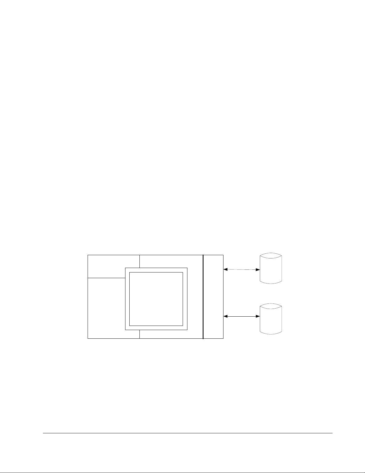
Application Domain
Real Time Domain
i.MX 7ULP
A7 Connectivity
Security
Secure JTAG
Internal Memory
256K RAM
UART x 4
I2C x4
3.3V/1.8V GPIO
USB2.0 HOST
(w/ HSIC)
Analog
2x 12 bit ADC
HAB – Secure Boot
Graphics
GC7000
NanoULTRA
External Memory
MMC5.0/SDIO x 2
16/32-bit LPDDR2/3
Power
Manager
SPI x 2
Arm Cortex -A7
NEON
Trust Zone
32KB I-cache 32KB D-cache
FPU
ETM
256KB L2 cache
Analog Comparators
External Memory
Quad SPI (OTFAD)
Timers
Watch Dog
32 bit Timer x4
System timers
Crypto / TRNG
FPUMPU
M4 Connectivity
UART x 4
I2C x4
3.3V/1.8V GPIO
SPI x2
FlexIO
2x 12 -bit DAC
Internal Memory
256K RAM
Timers
Watch Dog
32 bit Timer x4
System timers
Clock/Reset
Arm Cortex -
- M4
DAP
DSP Extensions
USB2.0 OTG
(w/ PHY)
8KB I/D
- cache
MIPI DSI
Display
Secure Fuse
FlexBUS
I2S x 2
eFuses / OTP
SEMA4 / Msg Unit
DMA
VIU
Camera
FlexIO
GC320
Composition
Security
uHAB – Secure Boot
Clock and Power
Management System
Secure
RTC
Tamper
Detection
Security – Batt Domain
Key
Storage
Crypto / TRNG
XRDC
Access and IPC
PLL/OSC
32K Secure
Memory
The following table provides examples of orderable sample part numbers covered by this data sheet.
Figure 1. i.MX 7ULP Block Diagram
Part Number Options Cortex-
MCIMX7U5DVP07SD GPU-2D,
i.MX 7ULP Applications Processor—Consumer, Rev. 0, 09/2020
GPU-3D
supported
Ordering information
A7
Speed
Grade
720 MHz 200 MHz Commercial
Cortex-
M4
Speed
Grade
Table continues on the next page...
Qualification
Tier
(Consumer)
Junction
Temperature
Range
0 to +95 °C 14 mm x 14 mm, 0.5 mm
pitch BGA, Package code
"VP"
Package
NXP Semiconductors
3
Page 4
Ordering information (continued)
Part Number Options Cortex-
A7
Speed
Grade
MCIMX7U5DVK07SD GPU-2D,
GPU-3D
supported
MCIMX7U3DVK07SD No GPU 720 MHz 200 MHz Commercial
720 MHz 200 MHz Commercial
Cortex-
M4
Speed
Grade
Qualification
Tier
(Consumer)
(Consumer)
Junction
Temperature
Range
0 to +95 °C 10 mm x 10 mm, 0.5 mm
pitch BGA, Package code
"VK"
0 to +95 °C 10 mm x 10 mm, 0.5 mm
pitch BGA, Package code
"VK"
Package
The following figure describes the part number nomenclature so users can identify the characteristics of the
specific part number.
Figure 2. i.MX 7 Family Part Number Definition
Related Resources
Type Description
Reference Manual The i.MX 7ULP Applications Processor Reference Manual contains a comprehensive description of
the structure and function (operation) of the SoC.
Data Sheet The Data Sheet includes electrical characteristics and signal connections.
Chip Errata The chip mask set errata provides additional or corrective information for a particular device mask
set.
Package drawing Package dimensions are provided in Package information and contact assignments
4
NXP Semiconductors
i.MX 7ULP Applications Processor—Consumer, Rev. 0, 09/2020
Page 5
The power mode acronyms used throughout this document are defined as follows.
Power mode acronym table
Power mode acronym Power mode name
HSRUN High-speed run mode
RUN Nominal speed run mode
VLPR Very low power run mode
PSTOP Partial stop mode
STOP Stop mode
VLPS Very low power stop mode
LLS Low leakage stop mode
VLLS Very low leakage stop mode
For details on each of these operating modes, see the i.MX 7ULP Applications Processor Reference Manual
(IMX7ULPRM).
i.MX 7ULP Applications Processor—Consumer, Rev. 0, 09/2020
5
NXP Semiconductors
Page 6

Table of Contents
1 i.MX 7ULP modules list......................................................... 8
2 Clocking................................................................................ 22
2.1 Introduction..................................................................22
2.2 Clock distribution......................................................... 23
2.3 External clock sources.................................................23
2.4 Oscillators....................................................................23
2.5 Internal clock sources..................................................24
3 Application domain (implementing ARM Cortex-A7).............25
3.1 Memory system—application domain..........................25
3.1.1 Internal memory (application domain)...........25
3.1.2 Multi Mode DDR Controller (MMDC).............25
3.1.3 eMMC............................................................26
3.2 Peripherals—application domain.................................26
3.2.1 Graphics processor human machine
interfaces.......................................................26
3.2.2 Security—application domain........................26
3.2.3 Timers—application domain..........................28
3.2.4 Connectivity and communications—
applications domain...................................... 28
4 Real-time domain (implementing ARM Cortex-M4).............. 28
4.1 Memory system—real-time domain.............................28
4.1.1 Internal memory—real-time domain..............28
4.1.2 QuadSPI flash...............................................29
4.2 Peripherals—real-time domain.................................... 29
4.2.1 Analog—real-time domain.............................29
4.2.2 Connectivity and communications—real-
time domain...................................................29
5 System control modules........................................................29
5.1 JTAG—system control.................................................30
5.2 JTAG device identification register.............................. 30
5.3 Oscillators and PLLs....................................................30
5.3.1 System oscillator (SYS OSC)........................30
5.3.2 Real-Time Clock Oscillator (RTC OSC)........30
5.3.3 USB PLL....................................................... 31
5.3.4 Fixed Frequency PLL (Fixed-freq PLL).........31
5.3.5 Fractional-N PLL (FracN PLL).......................31
5.4 Power Management.................................................... 31
5.4.1 Digital PMC................................................... 32
5.4.2 Analog power management controller
(Analog PMC)................................................32
6 i.MX 7ULP LDO Bypass versus LDO-enabled modes.......... 32
6.1 Real-time domain LDO Enabled mode........................32
6.2 Application domain LDO Enabled mode......................33
6.3 Application domain LDO BYPASS mode.................... 33
7 System specifications............................................................33
7.1 Ratings........................................................................ 33
7.1.1 Thermal handling ratings...............................33
7.1.2 Moisture handling ratings..............................34
7.1.3 ESD handling ratings.................................... 34
7.1.4 Absolute maximum ratings............................34
7.1.5 Recommended operating conditions—
system...........................................................35
7.1.6 Estimated maximum supply currents............ 39
7.2 System clocks..............................................................41
7.2.1 Clock modules...............................................41
7.2.2 Core, platform, and system bus clock
frequency limitations..................................... 43
7.2.3 Peripheral clock frequencies.........................44
7.2.4 PLL PFD output.............................................47
7.2.5 Audio tunable clock.......................................48
7.3 Power sequencing—system........................................ 49
7.3.1 Power-on sequencing................................... 49
7.3.2 Power-off sequencing................................... 50
7.4 Requirements for unused interfaces............................50
7.5 Electrical Characteristics and Thermal Specifications.51
7.5.1 AC electrical characteristics..........................51
7.5.2 Nonswitching electrical characteristics..........52
7.5.3 Switching electrical characteristics................54
7.5.4 Debug and trace modules.............................56
7.5.5 Thermal specifications.................................. 59
8 Specifications—application domain...................................... 61
8.1 Peripheral operating requirements and behaviors.......61
8.1.1 DDR timing—application domain.................. 61
8.1.2 Ultra-high-speed SD/SDIO/MMC host
interface (uSDHC) AC timing—application
domain.......................................................... 61
8.1.3 Flexbus switching specifications................... 66
8.1.4 Display, Video, and Audio Interfaces............ 69
8.1.5 Timer specifications—application domain.....70
8.1.6 Connectivity and communications
specifications—application domain...............70
9 Specifications—real-time domain..........................................79
9.1 Power sequencing—real-time domain.........................79
9.2 Peripheral operating requirements and behaviors—
real-time domain..........................................................80
9.2.1 QuadSPI AC specifications...........................80
9.2.2 Analog modules............................................ 84
9.2.3 Timer specifications—real-time domain........92
9.2.4 Connectivity and communications
specifications—real-time domain.................. 92
10 Package information and contact assignments.....................96
10.1 BGA, 14 x 14 mm, 0.5 mm pitch (VP suffix)................96
10.1.1 14 x 14 mm package case outline.................96
10.1.2 14 x 14 mm, 0.5 mm pitch, ball map............. 98
10.1.3 14 x 14 mm power supply and functional
contact assignments..................................... 100
10.2 BGA, 10 x 10 mm, 0.5 mm pitch (VK suffix)................108
10.2.1 10 x 10 mm package case outline.................108
10.2.2 10 x 10 mm, 0.5 mm pitch, ball map............. 110
6
NXP Semiconductors
i.MX 7ULP Applications Processor—Consumer, Rev. 0, 09/2020
Page 7

10.2.3 10 x 10 mm power supply and functional
contact assignments....................................112
11 Revision History.................................................................. 120
i.MX 7ULP Applications Processor—Consumer, Rev. 0, 09/2020
7
NXP Semiconductors
Page 8

i.MX 7ULP modules list
1 i.MX 7ULP modules list
The i.MX 7ULP applications processor contains a variety of digital and analog
modules. The following table describes these modules in alphabetical order.
In the Domain column in this table:
• AD = Application Power Domain (primarily controlled by the Cortex-A7)
• RT = Real-Time Power Domain (primarily controlled by the Cortex-M4)
• VBAT = RTC/VBAT power domain Real-Time Domain
• DGO = “always-on” DGO power domain
• SYS = system-level functions that are implemented separately from the domains
listed above.
Table 1. i.MX 7ULP modules list
Block Name Block Mnemonic Subsystem Power
AMBA Network
Interconnect Crossbar
Analog PMC
Analog-to-Digital
Converter
NIC0-1 DMA and Bus Fabrics AD The AMBA Network Interconnect
Analog PMC Power Management SYS The Analog PMC consists of voltage/
ADC0-1 Analog RT Analog-to-Digital Converter (ADC) is a
Table continues on the next page...
Brief description
Domain
Crossbar (NIC) is a highly configurable
and high performance AMBA-compliant
network infrastructure which arbitrates
between multiple AXI or AHB masters to
grant access to internal or external
memories or other slave devices. It
supports connectivity between several
slave and master ports for parallel
processing. It uses a hybrid round-robin
arbitration scheme and contains
frequency converters, data width
converters, bus protocol converter, and
AXI channel buffers.
current references, core logic supply
regulators, memory supply regulators,
Back and Forward Biasing regulators,
monitors and power switches, etc. There
are two Analog PMC subsystems in i.MX
7ULP, one associated with the M4 power
domain and the other with the A7 power
domain.
12-bit resolution, successive
approximation analog to digital
converter. The ADC module supports up
to 16 single-ended external analog
inputs. It outputs 12-bit, 10-bit, or 8-bit
digital signal in right-justified unsigned
8
NXP Semiconductors
i.MX 7ULP Applications Processor—Consumer, Rev. 0, 09/2020
Page 9

Table 1. i.MX 7ULP modules list (continued)
i.MX 7ULP modules list
Block Name Block Mnemonic Subsystem Power
Domain
format. The ADC can achieve 1
microsecond conversion rate.
Asynchronous
Wakeup Interrupt
Controller
Bit Manipulation
Engine
Comparator CMP0-1 Analog DGO The (CMP) module provides a circuit for
Cross Trigger Matrix CTM Debug RT Cross Trigger Matrix (CTM) is a
Cryptographic
Acceleration and
Assurance
AWIC System Control RT The Asynchronous Wakeup Interrupt
Controller (AWIC) module is capable of
interrupt detection and wake-up of a
processor when it is in low power mode.
BME Multicore peripherals
and resource domain
control submodules
CAAM Security AD Cryptographic Acceleration and
Table continues on the next page...
RT The Bit Manipulation Engine (BME)
provides hardware support for atomic
read-modify-write memory operations to
the peripheral address space. This
architectural capability is also known as
"decorated storage" as it defines a
mechanism for providing additional
semantics for load and store operations
to memory-mapped peripherals beyond
just the reading and writing of data
values to the addressed memory
locations.
comparing two analog input voltages.
The comparator circuit is designed to
operate across the full range of the
supply voltage (rail to rail operation).
component of the Embedded Cross
Trigger (ECT), which is key in the
multicore debug strategy. The CTM
receives signals from various sources
(i.e. cores and peripherals) and
propagates or routes them to the
different debug resources of the SoC.
Those debug resources can include time
stamping capability, real-time trace,
triggers and debug interrupts.
Assurance Module (CAAM) is a
multifunction accelerator that supports
the cryptographic functions common in
many security protocols. This includes
AES128, AES256, DES, 3DES, SHA1,
SHA224, SHA256, and a random
number generator with a true entropic
seed. CAAM includes a DMA engine that
is descriptor based to reduce processoraccelerator interaction. Security feature
clear keys and memories when on-chip
security monitor detects tampering. The
Secure RAM is implemented and
provides secure storage of sensitive
information both in on-chip RAM and in
Brief description
i.MX 7ULP Applications Processor—Consumer, Rev. 0, 09/2020
9
NXP Semiconductors
Page 10

i.MX 7ULP modules list
Table 1. i.MX 7ULP modules list (continued)
Block Name Block Mnemonic Subsystem Power
Domain
off-chip, nonvolatile memory. For details,
see the i.MX 7ULP Security Reference
Manual.
Cyclic Redundancy
Check
Debug Access Port DAP Debug RT Debug Port Access (DAP) provides
Digital PMC Digital PMC Power Management SYS The Digital PMC module allows user
Digital-to-Analog
Converter
Direct Memory
Access
Direct Memory
Access Multiplexer
CRC Connectivity and
Communications
DAC0-1 Analog RT Digital-to-Analog Converter (DAC) is the
DMA0-1 DMA and Bus Fabrics AD, RT Direct Memory Access (DMA) is capable
DMAMUX0-1 DMA and Bus Fabrics AD, RT The Direct Memory Access Multiplexer
Table continues on the next page...
RT The Cyclic Redundancy Check (CRC)
module is a hardware CRC generator
circuit using 16/32-bit shift register. The
CRC module supports error detection for
all single, double, odd, and most multibits errors, programmable initial seed
value, and optional feature to transpose
input data and CRC result via transpose
register.
debugger access to on-chip system
resources via the SWJ-DP port. The
DAP provides internal system access to
A7 Debug Port, M4 Debug Port, System
Bus, JTAG controller, and SoC Control
and Status. The DAP also enables
system access to CoreSight debug
subsystem through the APBIC port.
software to control power modes of the
chip and to optimize power consumption
for the level of functionality needed.
There are two instances of Digital PMC
on this device, one for each main power
domain.
12-bit resolution digital-to-analog
converters with programmable reference
generator output. The output of the DAC
can be placed on an external pin or set
as one of the inputs to the analog
comparator or ADC. The DAC is capable
of achieving 1 ms conversion rate for
high-speed signals and 2 ms conversion
rate for low-speed signals.
of performing complex data transfers
with minimal intervention from a host
processor. Each DMA module supports
32 DMA channels. The transfer control
descriptors for each of the 32 channels
locate in system memory. DMA0 is in the
real-time domain. DMA1 is in the
application domain.
(DMAMUX) module routes DMA
sources, called slots, to any of the
Brief description
10
NXP Semiconductors
i.MX 7ULP Applications Processor—Consumer, Rev. 0, 09/2020
Page 11

Table 1. i.MX 7ULP modules list (continued)
i.MX 7ULP modules list
Block Name Block Mnemonic Subsystem Power
Embedded Trace
FIFO
Embedded Trace
Router
Extended Resource
Domain Controller
External Bus Interface
ETF Debug RT The Embedded Trace FIFO (ETF)
ETR Debug RT The ETR is a trace sink that redirects the
XRDC Multicore Peripherals
and Resource Domain
Control submodules
FlexBus Memories and Memory
Controllers
Brief description
Domain
supported DMA channels. DMAMUX0 is
in the real-time domain. DMAMUX1 is in
the application domain.
consists of a formatter, control, and the
trace RAM. It is a configuration of the
Trace Memory Controller (TMC). The
ETF will have a memory size of
16Kbytes. The ETF and associated
memory should be connected in the
system such that it will retain the
information though a warm or cold reset
of the system. This is to allow for debug
information to be retained for debugging
problems that may arise and cause a
reset of the system.
trace stream onto the AXI bus to external
storage. It can utilize a single contiguous
region or a scattered allocation of blocks
for a circular buffer. Reading of the AXI
based trace buffer can either be done
directly over AXI from a normal bus
master. The ETR is a configuration
option of the TMC as is the ETF.
AD, RT The Extended Resource Domain
Controller (XRDC) provides an
integrated, scalable architectural
framework for access control, system
memory protection and peripheral
isolation. It allows software to assign
chip resources (like processor cores,
non-core bus masters, memory regions
and slave peripherals) to processing
domains, to support enforcement of
robust operational environments. The
XRDC implementation is distributed
across multiple submodules instantiated
throughout the device.
AD The External Bus Interface (FlexBus)
module provides external memory
expansion and provides connection to
external peripherals with a parallel,
memory-mapped interface. The FlexBus
supports asynchronous and
synchronous interface to external ROM,
NOR flash, SRAM, PSRAM,
programmable logic devices and other
memory-mapped slave devices.
Table continues on the next page...
i.MX 7ULP Applications Processor—Consumer, Rev. 0, 09/2020
11
NXP Semiconductors
Page 12

i.MX 7ULP modules list
Table 1. i.MX 7ULP modules list (continued)
Block Name Block Mnemonic Subsystem Power
External Watchdog
Monitor
Fast Internal
Reference Clock
Fixed-frequency PLL Fixed-Freq PLL
Flexible Input/Output FLEXIO0-1 Connectivity and
Fractional-N PLL Frac-N PLL
GC320 Composition
Processing Core
EWM Timers RT The External Watchdog Monitor (EWM)
FIRC Clock Sources and
Control
Clock Sources and
(PLL0)
(PLL1-3)
GPU-2D Multimedia AD Vivante GC320 is a Composition
Control
Communications
Clock Sources and
Control
Table continues on the next page...
Brief description
Domain
module is designed to monitor external
circuits, as well as the software flow.
This provides a back-up mechanism to
the internal WDOG that can reset the
system. The EWM differs from the
internal WDOG in that it does not reset
the system. The EWM, if allowed to timeout, provides an independent trigger pin
that when asserted resets or places an
external circuit into a safe mode.
SYS The Fast Internal Reference Clock
(FIRC) module is an internal oscillator
that can generate a reference clock in
the range from 48 MHz to 60 MHz. The
FIRC output clock is used as a reference
to the SCG module, and it is also used
as a clock option to most on-chip
modules.
SYS The Fixed-frequency PLL is the same as
the USB PLL. In addition to the main
clock output, this PLL also includes 4
Phase Fractional Dividers (PFDs) that
can generate other clock frequencies.
There is one instance of the Fixed-freq
PLL (PLL0) provides clocks for M4 core
and buses and peripherals in the Realtime domains.
AD, RT The Flexible Input/Output (FlexIO)
module is capable of supporting a wide
range of protocols including, but not
limited to: UART, I2C, SPI, I2S, camera
interface, display interface, PWM
waveform generation, etc. FlexIO0 is in
the real-time domain. FlexIO1 is in the
application domain.
SYS The Fractional-N (Frac-N) PLL can
generate an output clock of 528 MHz
from a supported reference clock. In
addition to the main clock output, this
PLL also includes up to 4 Phase
Fractional Dividers (PFDs) that can
generate other clock frequencies. This
PLL also supports tunable clock for
audio applications.
Processing Core (CPC) GPU. It supports
user interface rendering and performs
functions like blending, filtering, rotation,
12
NXP Semiconductors
i.MX 7ULP Applications Processor—Consumer, Rev. 0, 09/2020
Page 13

Table 1. i.MX 7ULP modules list (continued)
i.MX 7ULP modules list
Block Name Block Mnemonic Subsystem Power
GC7000 Nano Ultra
Graphic Processing
Unit
Hardware Semaphore SEMA42_0 and
Input/Output
Multiplexing
Controller
Internal Reference
Clock 1kHz
Joint Test Action
Group Controller
LCD Interface
Controller
GPU-3D Multimedia AD i.MX 7ULP integrates the Vivante
Multicore Peripherals
SEMA42_1
IOMUXC0-1 &
IOMUXC_DDR
IRC1K Clock Sources and
JTAGC Debug RT Joint Test Action Group Controller
LCDIF Multimedia AD The LCDIF is a general purpose display
and Resource Domain
Control submodules
System Control AD, RT The Input/Output Multiplexing Controller
Control
Table continues on the next page...
Brief description
Domain
overlay, resizing, transparency, and
other dynamic effects.
GC7000 Nano Ultra Graphic Processing
Unit (GPU-3D). supporting OpenGL
ES2.0/1.1, Desktop OpenGL 2.1,
OpenVG1.1, and GLSL shading
language support.
AD, RT The Hardware Semaphore (SEMA42)
module provides the hardware support
needed in multicore systems for
implementing semaphores and provide a
simple mechanism to achieve "lock/
unlock" operations via a single write
access. SEMA42_0 is in the real-time
domain. SEMA42_1 is in the application
domain.
(IOMUXC) enables the chip to share one
pad for multiple signals from different
peripheral interfaces. This pad sharing
mechanism is done by multiplexing the
pad's input and output signals. The
IOMUXC also controls the pads setting
parameters and digital filter functions of
the pad. In addition, the IOMUXC
controls input multiplexing logic for input
signals multiplexed at multiple locations.
IOMUXC0 is in the real-time domain.
IOMUXC1 and IOMUXC_DDR are in the
application domain.
SYS The Internal Reference Clock 1kHz
(IRC1K) module is an internal oscillator
that can generate a reference clock of
1kHz. The IRC1K clock is enabled in all
modes of operation, including all low
power modes.
(JTAGC) provides the means to test chip
functionality and connectivity while
remaining transparent to system logic
when not in test mode. Testing is
performed via a boundary scan
technique, as defined in the IEEE
1149.1-2001 standard.
controller used to drive a wide range of
display devices varying in size and
capabilities. The LCDIF is used as a
i.MX 7ULP Applications Processor—Consumer, Rev. 0, 09/2020
13
NXP Semiconductors
Page 14

i.MX 7ULP modules list
Table 1. i.MX 7ULP modules list (continued)
Block Name Block Mnemonic Subsystem Power
Low-Leakage WakeUp Unit
Low Power InterIntegrated Circuit
Low Power Periodic
Interrupt Timer
Low Power Serial
Peripheral Interface
Low-power Trusted
Cryptography
LLWU System Control DGO The Low-Leakage Wake-Up Unit (LLWU)
LPI2C0-7 Connectivity and
Communications
LPIT0-1 Timers AD, RT Low Power Periodic Interrupt Timer
LPSPI0-3 Connectivity and
Communications
LTC Security RT Low-power Trusted Cryptography is an
Brief description
Domain
bridge between the DSI controller and
the NIC0 crossbar.
module allows user to select up to 32
external pin sources and up to 8 internal
modules as a wakeup source from low
leakage power modes.
AD, RT The Low Power Inter-Integrated Circuit
(LPI2C) module implements an efficient
interface to an I2C bus as a master. The
LPI2C can continue operating while the
processor is in stop mode provided an
appropriate peripheral clock is available.
This module is designed for low CPU
overhead with DMA offloading of FIFO
register accesses. LPI2C0 - LPI2C3 are
in the real-time domain. LPI2C4 LPI2C7 are in the application domain.
(LPIT) is a multichannel timer module
that can generate independent pretrigger and trigger outputs. These timer
channels can operate individually or can
be chained together. The pre-trigger and
trigger outputs can be used to trigger
other modules on the device. The LPIT
can also operate in low power modes.
LPIT0 is in the real-time domain. LPIT1
is in the application domain.
AD, RT The Low Power Serial Peripheral
Interface (LPSPI) module implements an
efficient interface to an SPI bus as a
master and/or a slave. The LPSPI can
continue operating while the processor is
in stop mode if an appropriate peripheral
clock is available. This module is
designed for low CPU overhead with
DMA offloading of FIFO register
accesses. LPSPI0 and LPSPI1 are in the
real-time domain. LPSPI2 and LPSPI3
are in the application domain.
architecture that allows multiple
cryptographic hardware accelerator
engines to be instantiated and share
common registers. This version of LTC
supports 128-bit AES. For details, see
the i.MX 7ULP Security Reference
Manual.
14
NXP Semiconductors
Table continues on the next page...
i.MX 7ULP Applications Processor—Consumer, Rev. 0, 09/2020
Page 15

Table 1. i.MX 7ULP modules list (continued)
i.MX 7ULP modules list
Block Name Block Mnemonic Subsystem Power
Low Power Universal
Asynchronous
Receiver/Transmitter
Low Power Timer
Memory-Mapped
Cryptographic
Acceleration Unit
Messaging Unit MU Multicore Peripherals
MIPI Display Serial
Interface Controller
MIPI Display Serial
Interface Physical
Layer
LPUART0-7 Connectivity and
Communications
LPTMR0-1 Timers DGO The Low Power Timer (LPTMR) module
MMCAU Security RT Memory-Mapped Cryptographic
and Resource Domain
Control submodules
DSI Controller Multimedia AD The MIPI Display Serial Interface
DSI PHY Multimedia AD The MIPI Display Serial Interface
Table continues on the next page...
Brief description
Domain
AD, RT The Low Power Universal Asynchronous
Receiver/Transmitter (LPUART) module
provides asynchronous, serial
communication capability with external
devices. LPUART supports non-returnto-zero (NRZ) encoding format and IrDAcompatible infrared (low-speed) SIR
format. The LPUART can continue
operating while the processor is in stop
mode if an appropriate peripheral clock
is available. This module is designed for
low CPU overhead with DMA offloading
of FIFO register accesses. LPUART0 –
LPUART3 are in the real-time domain.
LPUART4 – LPUART7 are in the
application domain.
is a 16-bit timer which operates as realtime interrupt or pulse accumulator. This
LPTMR module can remain functional
when the chip is in low power modes,
provided the reference clock to this timer
is active.
Acceleration Unit (MMCAU) is an
optimized security accelerator that
supports the cryptographic functions
common in many security protocols. This
includes DES, 3DES, AES, MD5, SHA-1,
SHA-256 algorithms via simple C calls to
optimized security functions.
RT Messaging Unit (MU) is a shared
peripheral with a 32-bit IP bus interface
and interrupt request signals to each
host processor. The MU exposes a set
of registers to each processor which
facilitate inter-processor communication
via 32-bit words, interrupts and flags.
Interrupts may be independently masked
by each processor to allow polled-mode
operation.
Controller (DSI Controller) is responsible
for serializing display data from the GPU.
Data can come from either the GPU or
the processor/DMA controller.
Physical Layer (DSI PHY) is a two-lane
interface that supports up to 1 Gbps of
data on each lane. DSI PHY includes a
i.MX 7ULP Applications Processor—Consumer, Rev. 0, 09/2020
15
NXP Semiconductors
Page 16

i.MX 7ULP modules list
Table 1. i.MX 7ULP modules list (continued)
Block Name Block Mnemonic Subsystem Power
Multicore System
Mode Controller
Multi Mode DDR
Controller
On-The-Fly AES
Decryption
Peripheral Clock
Control
Reset Mode
Controller
On-Chip One-TimeProgrammable
Controller
MSMC System Control DGO Multicore System Mode Controller
MMDC Memories and Memory
Controllers
OTFAD Security RT The On-The-Fly AES Decryption
PCC0-3 Clock Sources and
Control
RMC System Control DGO Reset Mode Controller (RMC)
OCOTP_CTRL System Control RT The On-Chip One-Time-Programmable
Table continues on the next page...
Brief description
Domain
PLL which output clock is dedicated DSI
uses.
(MSMC) is responsible for sequencing
the system into and out of all low power
Stop and Run modes. MSMC monitors
events to trigger transitions between
power modes, while controlling the
power, clocks, and memories of the
system to achieve the power
consumption and functionality of that
mode.
AD The Multi Mode DDR Controller (MMDC)
is a configurable DDR controller that
provides interface to LPDDR2 or
LPDDR3 memory. The MMDC consists
of a core and PHY. The core is
responsible for communication with the
system through AXI interface, DDR
commands generation, DDR command
optimizations, and read/ write data path.
The PHY performs timing adjustment
using special calibration mechanisms to
ensure data capture margin at the
supported clock rate.
(OTFAD) module provides an advanced
hardware implementation that minimizes
any incremental cycles of latency
introduced by the decryption in the
overall external memory access time.
The OTFAD engine also includes
complete hardware support for a
standard AES key unwrap mechanism to
decrypt a key BLOB data instruction
containing the parameters needed for up
to 4 unique AES contexts.
AD, RT The Peripheral Clock Control (PCC)
module is responsible for clock selection,
optional division and clock gating mode
for peripherals in their respected power
domain. PCC0 and PCC1 are in the realtime domain. PCC2 and PCC3 are in the
application domain.
implements reset modes and reset
functions of the chip.
Controller (OCOTP_CTRL) module
provides an interface for reading,
16
NXP Semiconductors
i.MX 7ULP Applications Processor—Consumer, Rev. 0, 09/2020
Page 17

Table 1. i.MX 7ULP modules list (continued)
i.MX 7ULP modules list
Block Name Block Mnemonic Subsystem Power
Domain
programming and/or overriding
identification and control information
stored in on-chip fuse elements. The
module supports electricallyprogrammable poly fuses. The
OCOTP_CTRL also provides a set of
volatile software-accessible signals
which can be used for software control of
hardware elements, not requiring nonvolatility.
Peripheral Trigger
Multiplexing
Port Control PCTL_A-F System Control AD, RT The Port Control (PCTL) module
Quad Serial
Peripheral Interface
Rapid GeneralPurpose Input and
Output
Read-only memory
Controller
Real Time Clock
Oscillator
Single Wire Output SWO Debug RT Single Wire Output (SWO) is a trace
TRGMUX0-1 System Control AD, RT Peripheral Trigger Multiplexing
(TRGMUX) TRGMUX0 is in the real-time
domain. TRGMUX1 is in the application
domain.
provides control for GPIO interrupt
function. GPIO interrupt can be
configured independently for each pin in
the 32-bit port. There is one instance of
the PCTL module for each port. PCTL_A
and PCTL_B are in the real-time domain.
PCTL_C - PCTL_F are in the application
domain.
QSPI Memories and Memory
Controllers
RGPIO2P0-1 System Control AD, RT The Rapid General-Purpose Input and
ROMCP0/1 Memories and Memory
Controllers
RTC OSC Clock Sources and
Control
Table continues on the next page...
RT The Quad Serial Peripheral Interface
(QSPI) module provides an interface to
various types of serial flash memory.
The QSPI interface allows one serial
flash connection. It supports 1-bit, 4-bit
and 8-bit SPI bus width.
Output with 2 Ports (RGPIO2P) is similar
to the RGPIO module, except it has an
AHB-lite port, in addition to the IPS port,
for faster access. RGPIO2P0 is in the
real-time domain. RGPIO2P1 is in the
application domain.
AD, RT A ROM controller and boot ROM are
present in for both the A7 and M4 CPU
cores. ROMCP0 and a 64 kB ROM are
in the real-time domain. ROMCP1 and a
96 kB ROM are in the application
domain.
VBAT The Real Time Clock Oscillator (RTC
OSC) module provides the clock source
for the Real-Time Clock module. The
RTC OSC module, in conjunction with an
external crystal, generates a 32.678 kHz
reference clock for the RTC.
data drain that acts as bridge between
Brief description
i.MX 7ULP Applications Processor—Consumer, Rev. 0, 09/2020
17
NXP Semiconductors
Page 18

i.MX 7ULP modules list
Table 1. i.MX 7ULP modules list (continued)
Block Name Block Mnemonic Subsystem Power
Secure JTAG
Controller
Secure Non-Volatile
Storage
Slow Internal
Reference Clock
Synchronous Audio
Interface
System Clock
Generation
SJC Debug RT The Secure JTAG Controller (SJC) is an
SNVS Security VBAT The Secure Non-Volatile Storage
SIRC Clock Sources and
Control
SAI0-1 Multimedia RT The Synchronous Audio Interface (SAI)
SCG0-1 Clock Sources and
Control
Table continues on the next page...
Brief description
Domain
the on-chip trace data to a data stream
that is captured by the Trace Port
Analyzer. It is a TPIU-like device that
supports a limited subset of the full TPIU
functionality for a simple debug solution.
authenticated debug module that
implements a challenge/response
mechanism using a standard
cryptographic algorithm. This allows post
production silicon debug without
compromising security requirements.
The SJC is connected in parallel with the
JTAGC module, but it is only used for
authenticated debug.
(SNVS) module is designed to safely
hold security-related data such as
cryptographic key, time counter,
monotonic counter, and general purpose
security information. A part of the SNVS
module belongs to the VBAT domain
that has its own dedicated power supply
which is always on. This enables SNVS
to keep this data valid and continue to
increment the time counter when the
power goes down in the rest of the SoC.
SNVS includes the Real-Time Clock
(RTC) module, which provides 64-bit
monotonic counter with roll-over
protection, 32-bit seconds counter with
roll-over protection and 32-bit alarm.
SYS The Slow Internal Reference Clock
(SIRC) module is an internal oscillator
that can generate a reference clock of 16
MHz. The SIRC output clock is used as
a reference to the SCG module, and it is
also used as a clock option to most onchip modules.
module implements full-duplex serial
interfaces with frame synchronization
such as I2S, AC97, and CODEC/DSP
interfaces.
AD, RT The System Clock Generation (SCG)
module is responsible for clock
generation and distribution across this
device. Functions performed by the SCG
include: clock reference selection,
generation of clock used to derive
18
NXP Semiconductors
i.MX 7ULP Applications Processor—Consumer, Rev. 0, 09/2020
Page 19

Table 1. i.MX 7ULP modules list (continued)
i.MX 7ULP modules list
Block Name Block Mnemonic Subsystem Power
Domain
processor, system, peripheral bus and
external memory interface clocks; source
selection for peripheral clocks; and,
control of power saving clock gating
mode. SCG0 is in the real-time domain.
SCG1 is in the application domain.
System Integration
Module
System Oscillator SYS OSC Clock Sources and
Tightly-Coupled
Memory
Timer/Pulse Width
Modulation
TimeStamp
Components
Timestamp timer TSTMR Timers AD, RT The TSTMR module is a free running
SIM System Control AD, RT The System Integration Module (SIM)
provides system control and chip
configuration registers. The SIM includes
the TSTMR module.
SYS The System Oscillator (SYS OSC)
Control
TCM Memories and Memory
Controllers
LPTPM0-7 Timers AD, RT The Timer/Pulse Width Modulation
TimeStamp
Components
Debug RT The timestamp components generate
RT Tightly Coupled Memory (TCM) RAM.
module is a crystal oscillator. The SYS
OSC, in conjunction with an external
crystal or resonator, generates a
reference clock for this device. It also
optionally supports an external input
clock provided to EXTAL signal directly.
This RAM is tightly integrated to the M4
processor. M4 accesses this memory
with zero wait-state. There is a backdoor
port that allows M4 DMA and other bus
masters in the SoC to access this
memory.
Module (TPM) is a multichannel timer
module that supports input capture,
output compare, and the generation of
PWM signals. The counter, compare and
capture registers are clocked by an
asynchronous clock that can remain
enabled in low power modes. LPTPM0 –
LPTPM3 are in the real-time domain.
LPTPM4 – LPTPM7 are in the
application domain.
and distribute a consistent timestamp
value for multiple processors and other
blocks in a SoC.
incrementing counter that starts running
after system reset de-assertion and can
be read at any time by the software for
determining the software ticks. The
TSTMR is a 64-bit clock cycle counter. It
runs off the 1 MHz clock and resets on
every system reset. The counter only
stops when the clock to the TSTMR is
disabled.
Brief description
Table continues on the next page...
i.MX 7ULP Applications Processor—Consumer, Rev. 0, 09/2020
19
NXP Semiconductors
Page 20

i.MX 7ULP modules list
Table 1. i.MX 7ULP modules list (continued)
Block Name Block Mnemonic Subsystem Power
Domain
Trace Funnel FUNL Debug RT The Trace Funnel (FUNL) is used when
there is more than one trace source. The
Trace Funnel combines multiple trace
streams onto a single ATB bus. The
Trace Funnel includes an arbiter that
determines the priority of the ATB inputs.
Trace Port Interface
Unit
Trace Replicator Replicator Debug RT The Trace Replicator (Replicator)
True Random
Number Generator
ultra Secured Digital
Host Controller
Universal Serial Bus
High-Speed Inter
Chip Physical Layer
Universal Serial Bus
On-The-Go
TPIU Debug RT Trace Port Interface Unit (TPIU) acts as
a bridge between on-chip trace data, ID
distinguishable, and a TPA. It receives
ATB trace data and sends it off chip via
ARM’s standard trace interface. The
TPIU includes ATB interface, APB
interface, Formatter, Asynchronous
FIFO, Register bank, Trace out
serializer, and a pattern generator.
enables two trace sinks (TPIU and TMC)
to be wired together and receive ATB
trace data from the same trace source. It
takes incoming data from a single source
and replicates it to two master ports.
TRNG Security RT The True Random Number Generator
(TRNG) module is to generate high
quality, cryptographically secure, random
data. The TRNG module is capable of
generating its own entropy using an
integrated ring oscillator. In addition, the
module’s NIST certifiable PseudoRandom Number Generator (PRNG)
provides accelerated processing of
pseudo-random data.
uSDHC0/1 Memories and Memory
Controllers
HSIC-PHY Connectivity and
Communications
USB-OTG Connectivity and
Communications
Table continues on the next page...
AD The ultra Secured Digital Host Controller
(uSDHC) provides the interface between
the host system and SD, SDIO or eMMC
cards. The uSDHC acts as a bridge,
passing host bus transactions to the
cards by sending commands and
performing data accesses to/from the
cards or devices. It handles SD, SDIO
and eMMC protocol at transmission
level.
AD USB High-Speed Inter Chip Physical
Layer (HSIC-PHY) is a complete digital
IP designed to implement USB 2.0 HSIC
connectivity interface.
AD The Universal System Bus On-The-Go
(USB-OTG) module is a USB 2.0compliant implementation. The registers
and data structures of this USB
controller are based on the Enhanced
Brief description
20
NXP Semiconductors
i.MX 7ULP Applications Processor—Consumer, Rev. 0, 09/2020
Page 21

Table 1. i.MX 7ULP modules list (continued)
i.MX 7ULP modules list
Block Name Block Mnemonic Subsystem Power
Domain
Host Controller Interface Specification
for Universal Serial Bus (EHCI). This
module can act as a host, a device or an
On-The-Go negotiable host/device on
the USB bus.
Universal Serial Bus
Phase Locked Loop
Universal Serial Bus
Physical Layer
Video Input Unit VIU Multimedia AD The Video Input Unit (VIU) provides a
Wakeup Unit WKPU System Control AD Wakeup Unit (WKPU) module is capable
Watchdog Timer WDOG0-2 Timers AD, RT The Watchdog Timer (WDOG) module
USB PLL Clock Sources and
Control
USB-PHY Connectivity and
Communications
Table continues on the next page...
AD USB Phase Locked Loop (USB PLL) is
embedded in the USB transceiver block.
This PLL allows an exact 480 MHz to be
generated from a supported reference
clock of 24 MHz. The output of this PLL
is primarily used for PLL operation. The
USB PLL clock is also made available as
a clock source for other peripherals in
the SoC.
AD The Universal System Bus Physical
Layer (USB-PHY) implements USB
physical layer connecting to USB host/
device systems at low-speed, full-speed,
and high-speed. USB-PHY provides a
standard UTMI interface for connection
to the USB-OTG controller.
parallel interface for digital video. The
VIU accepts various types of digital
video input on its parallel interface,
decodes it and optionally performs
processes such as down-scaling,
horizontal up-scaling, brightness and
contrast adjustment, pixel format
conversion, deinterlacing and horizontal
mirroring. The resultant video stream is
then stored to system memory for
subsequent post-processing and display.
of interrupt detection and wake-up of the
Cortex-A processor when it is in low
power mode.
keeps a watch on the system functioning
and resets it in case of its failure.
Reasons for failure include run-away
software code and the stoppage of the
system clock that in a safety critical
system can lead to serious
consequences. In such cases, the
WDOG brings the system into a safe
state of operation. The WDOG monitors
the operation of the system by expecting
periodic communication from the
software, generally known as servicing
Brief description
i.MX 7ULP Applications Processor—Consumer, Rev. 0, 09/2020
21
NXP Semiconductors
Page 22

Clocking
Table 1. i.MX 7ULP modules list (continued)
Block Name Block Mnemonic Subsystem Power
XRDC Manager MGR Multicore Peripherals
and Resource Domain
Control submodules
XRDC Master Domain
Assignment Controller
XRDC Memory
Region Controller
XRDC Peripheral
Access Controller
MDAC Multicore Peripherals
and Resource Domain
Control submodules
MRC Multicore Peripherals
and Resource Domain
Control submodules
PAC Multicore Peripherals
and Resource Domain
Control submodules
Brief description
Domain
or refreshing the WDOG. If this periodic
refreshing does not occur, the WDOG
resets the system. WDOG0 is in the realtime domain. WDOG1 and WDOG2 are
in the application domain.
RT The XRDC Manager (MGR) submodule
coordinates all programming model
reads and writes.
AD, RT The XRDC Master Domain Assignment
Controller (MDAC) submodule handles
resource assignments and generation of
the domain identifiers.
AD, RT The XRDC Memory Region Controller
(MRC) submodule implements the
access controls for slave memories
based on the pre-programmed region
descriptor registers.
AD, RT The XRDC Peripheral Access Controller
(PAC) implements the access controls
for slave peripherals based on the preprogrammed domain access control
registers.
2 Clocking
2.1 Introduction
This section details the clock sources, distribution and management within the i.MX
7ULP. These functions are under joint control of the System Clock Generation (SCG)
modules, Peripheral Clock Control (PCC) modules, and Core Mode Controller (CMC)
blocks.
NOTE
References in this chapter to “Core 0” or “Processor A”
correspond to the Cortex M4 core. References in this chapter
to “Core 1” or “Processor B” correspond to the Cortex A7
core.
22
NXP Semiconductors
i.MX 7ULP Applications Processor—Consumer, Rev. 0, 09/2020
Page 23

Clocking
The clocking scheme provides clear separation between M4 domain and A7 domain.
Except for a few clock sources shared between two domains, such as the System
Oscillator clock, the Slow IRC (SIRC), and the Fast IRC clock (FIRC), clock sources
and clock management are separated and contained within each domain.
M4 clock management consists of SCG0, PCC0, PCC1, and CMC0 modules.
A7 clock management consists of SCG1, PCC2, PCC3, and CMC1 modules.
2.2 Clock distribution
The SCG modules generate and distribute clocks on the device. SCG functions
include:
• clock reference selection
• generation of clock used to derive processor, system, peripheral bus and external
memory interface clocks
• source selection for peripheral clocks
• control of power-saving clock-gating mode
PCC modules control clock selection, optional division and clock gating mode for
peripherals.
NOTE
• To bypass system oscillator and directly apply clock
from pin, SCG_SOSCCFG[EREFS] should be set to 0.
The direct clock should be applied on the EXTAL pin.
• For using oscillator reference,
SCG_SOSCCSR[SOSCEN] and
SCG_SOSCCFG[EREFS] should both be set to 1.
2.3
External clock sources
In normal functional mode, this device operates off two primary external reference
clocks: System oscillator clock (SOSC) and RTC oscillator clock (ROSC):
• System oscillator clock is a high frequency reference clock with a frequency in
the range of 16 MHz to 32 MHz. This clock is used as a reference clock to the onchip PLLs which generate all the required high frequency clocks.
• RTC oscillator clock is the 32.768 kHz constant frequency, real-time clock.
i.MX 7ULP Applications Processor—Consumer, Rev. 0, 09/2020
23
NXP Semiconductors
Page 24

Clocking
2.4 Oscillators
The system oscillator, in conjunction with an external crystal or resonator, generates a
reference clock for the device. The system oscillator module supports 16-32 MHz
crystals or resonators. It also provides the option for an external input clock to EXTAL
signal directly.
The RTC oscillator is in the VBAT domain. The RTC oscillator module, in conjunction
with an external crystal, generates a 32.768 kHz real-time reference clock for the RTC
and will always be enabled and supplying clock to SRTC. This is the default clock
source.
2.5
Internal clock sources
This device is capable of generating these internal reference clocks:
• The FIRC is the fast IRC clock with nominal frequency in the range from 48 to 60
MHz. In addition, the FIRC provides a clock selection option for peripherals.
• The SIRC is the slow IRC clock with nominal frequency of 16 MHz. The SIRC
provides a clock selection option for peripherals.
• The IRC1K generates 1 kHz clock that is enabled in all modes of operation,
including all low power modes.
• The RTC OSC has the capability to provide nominal 32 kHz (not recommended for
accurate clock and normal operation) IRC in absence of the external OSC reference
clock if the VBAT domain is enabled.
NOTE
The internal oscillator is automatically multiplexed in the
clocking system when the system detects a loss of clock. The
internal oscillator will provide clocks to the same on-chip
modules as the external 32 kHz oscillator. The internal
oscillator is not precise relative to a crystal. While it will
provide a clock to the system, it generally will not be precise
enough for long-term time keeping. The internal oscillator is
anticipated to be useful for quicker start-up times and
tampering prevention, but should not be used as the exclusive
source for the 32 kHz clocks. An external 32 kHz clock
source must be used for production systems.
24
NXP Semiconductors
i.MX 7ULP Applications Processor—Consumer, Rev. 0, 09/2020
Page 25

Application domain (implementing ARM Cortex-A7)
3 Application domain (implementing ARM Cortex-A7)
The application domain is built around an ARM Cortex-A7 processor optimized to
run nominally at 500 MHz, supported by a 32 KB L1 instruction and data cache, a
large L2 cache, and an LPDDR2/LPDDR3 memory interface. The Cortex-A7
processor is a high-performance low-power processor that implements the ARMv7-A
architecture. It uses the generic interrupt controller (GIC), generic 64-bit OS timer,
FPU and the ARM NEON SIMD engine. Additionally, all the optional debug features
are included.
3.1
Memory system—application domain
3.1.1 Internal memory (application domain)
3.1.2 Multi Mode DDR Controller (MMDC)
The Multi Mode DDR Controller is a dedicated interface to LPDDR2/LPDDR3
SDRAM.
The i.MX 7ULP MMDC is compatible with the following JEDEC-compliant memory
types:
• LPDDR2 SDRAM compliant to JESD209-2F LPDDR2 JEDEC standard released
June, 2013
• LPDDR3 SDRAM compliant to JESD209-3C JEDEC standard released August,
2015
MMDC operation with the standards stated above is contingent upon the board DDR
design adherence to the DDR design and layout requirements stated in the Hardware
Development Guide for the i.MX 7ULP Applications Processor (IMX7ULPHDG).
NOTE
For more information on MMDC, please refer to the
following Engineering Bulletin: EB00913 - LPDDR2/
LPDDR3 Parameter Optimizations for i.MX 7ULP.
i.MX 7ULP Applications Processor—Consumer, Rev. 0, 09/2020
25
NXP Semiconductors
Page 26
Application domain (implementing ARM Cortex-A7)
The table below shows the supported LPDDR2/LPDDR3 configurations:
Table 2. i.MX 7ULP supported LPDDR2/LPDDR3 configurations
Parameter LPDDR2 LPDDR3
Clock frequency up to 380.16 MHz
Bus width x16/x32
Channel Single
Chip select Up to two
3.1.3 eMMC
eMMC is a managed NAND device.
See Ultra-high-speed SD/SDIO/MMC host interface (uSDHC) AC timing—application
domain.
3.2
Peripherals—application domain
3.2.1 Graphics processor human machine interfaces
The i.MX 7ULP Application Domain implements the following graphics processor
human machine interfaces:
• 3D graphics processing unit (GPU-3D)
• 2D graphics processing unit (GPU-2D)
• MIPI Display Serial Interface Controller (MIPI DSI)
• Video Interface Unit (VIU)
See the i.MX 7ULP modules list for more details.
3.2.2
3.2.2.1 True Random Number Generator (TRNG)
The TRNG module is used to generate high quality, cryptographically secure, random
data. The TRNG module is capable of generating its own entropy using an integrated
ring oscillator. In addition, the module’s Pseudo-Random Number Generator (PRNG)
provides accelerated processing of pseudo-random data.
Security—application domain
26
NXP Semiconductors
i.MX 7ULP Applications Processor—Consumer, Rev. 0, 09/2020
Page 27
S
NVS
CAAM
Core Processor
HAB
R
O
M
Flash
RAM
Application domain (implementing ARM Cortex-A7)
3.2.2.2 Real-Time Clock (RTC)
The RTC module provides 64-bit monotonic counter with roll-over protection, 32-bit
seconds counter with roll-over protection and 32-bit alarm. This timer module is
extremely low power that allows it to operate on a backup power supply when the
main power supply is cut off. The RTC remains functional in all low power modes
and can generate an interrupt to exit any low power mode.
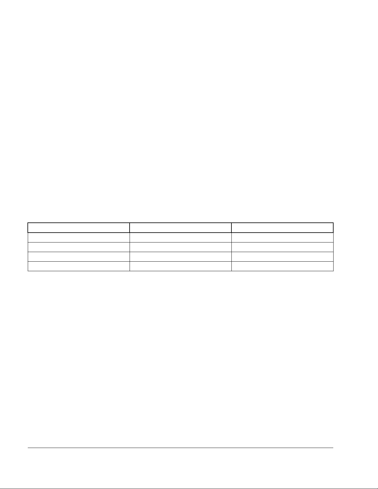
3.2.2.3 High Assurance Boot (HAB)
The High Assurance Boot (HAB) component of the ROM protects against the
potential threat of attackers modifying areas of code or data in programmable memory
to make it behave in an incorrect manner. The HAB also prevents attempts to gain
access to features which should not be available.
The integration of the HAB feature with the ROM code ensures that the chip does not
enter an operational state if the existing hardware security blocks have detected a
condition that may be a security threat or areas of memory deemed to be important
have been modified. The HAB uses RSA digital signatures to enforce these policies.
Figure 3. Secure Boot Components
NXP provides a reference Code Signing Tool (CST) for key
generation, certificate generation and code signing for use
i.MX 7ULP Applications Processor—Consumer, Rev. 0, 09/2020
with the HAB library. The CST can be found by searching
for "IMX_CST_TOOL" at http://www.nxp.com.
NOTE
27
NXP Semiconductors
Page 28

Real-time domain (implementing ARM Cortex-M4)
NOTE
For further details on making use of the secure boot feature
using HAB, contact your local NXP representative.
3.2.3 Timers—application domain
The i.MX 7ULP Application Domain implements the following timers:
• Low Power Periodic Interrupt Timer (LPIT)
• Timer/PWM Module (LPTPM)
• Low Power Timer (LPTMR)
• External Watchdog Monitor (EWM)
• Time stamp timer module (TSTMR)
• WDOG (Watchdog Timer)
See i.MX 7ULP modules list for more details.
3.2.4 Connectivity and communications—applications domain
The i.MX 7ULP Application Domain implements the following connectivity and
communications peripherals:
• Secure Digital (SD) Interface via the uSDHC
• Low Power Universal Asynchronous Receiver/Transmitter (LPUART)
• Low Power Inter-Integrated Circuit (LPI2C)
• Low Power Serial Peripheral Interface (LPSPI)
• Universal System Bus On-The-Go (USB-OTG)
• USB High-Speed Inter-Chip Physical Layer (HSIC-PHY)
See i.MX 7ULP modules list for more details.
4
Real-time domain (implementing ARM Cortex-M4)
The real-time domain is built around an ARM Cortex-M4 processor that contains a
floating-point unit and is optimized for lowest possible leakage.
4.1
28
NXP Semiconductors
Memory system—real-time domain
i.MX 7ULP Applications Processor—Consumer, Rev. 0, 09/2020
Page 29

System control modules
4.1.1 Internal memory—real-time domain
The real-time domain contains 256 kB of SRAM organized in sub-blocks of 32 kB
each. Each sub-block can be power-gated under software control to optimize power
consumption.
4.1.2 QuadSPI flash
The Quad Serial Peripheral Interface (QSPI) module provides an interface to various
types of serial flash memory. It allows one serial flash connection and supports 1-bit,
4-bit and 8-bit SPI bus width.
4.2
Peripherals—real-time domain
4.2.1 Analog—real-time domain
The i.MX 7ULP Real-Time Domain implements the following analog peripherals:
• 12-bit Analog to Digital Converter
• 12-bit Digital to Analog Converter
• Comparators
See i.MX 7ULP modules list for more details.
4.2.2
The i.MX 7ULP Real-Time Domain implements the following connectivity and
communications peripherals:
• Low Power Universal Asynchronous Receiver/Transmitter (LPUART)
• Low Power Inter-Integrated Circuit (LPI2C)
• Low Power Serial Peripheral Interface (LPSPI)
• Rapid General-Purpose Input and Output with 2 Ports (RGPIO2P)
• Flexible Input/Output (FlexIO)
Connectivity and communications—real-time domain
See the i.MX 7ULP modules list for more details.
System control modules
5
i.MX 7ULP Applications Processor—Consumer, Rev. 0, 09/2020
29
NXP Semiconductors
Page 30
System control modules
5.1 JTAG—system control
Joint Test Action Group Controller (JTAGC) provides the means to test chip
functionality and connectivity while remaining transparent to system logic when not in
test mode. Testing is performed via a boundary scan technique, as defined in the IEEE
1149.1-2001 standard.
5.2 JTAG device identification register
The device identification register (JTAG ID) allows the revision number and part
number to be read through the TAP. See the device identification register section of the
i.MX 7ULP Applications Processor Reference Manual for details. This table shows the
Part Identification Number (PIN) and the Part Revision Number (PRN) for each i.MX
7ULP silicon revision.
Table 3. JTAG device identification register information
Silicon Revision Part Identification Number (PIN) Part Revision Number (PRN)
A0 10'b0011100001 4’b0000
B0 10'b0011100001 4’b0001
B1 10'b0011100001 4’b0010
B2 10'b0011100001 4’b0011
The contents of the JTAD ID register are also mirrored in a SIM register called
JTAG_ID_REG (address 0x410A_308C).
5.3
Oscillators and PLLs
5.3.1 System oscillator (SYS OSC)
The system oscillator (SYS OSC) is a crystal oscillator. The SYS OSC, in conjunction
with an external crystal or resonator, generates a reference clock for this chip. It also
provides the option for an external input clock to EXTAL signal directly.
30
NXP Semiconductors
i.MX 7ULP Applications Processor—Consumer, Rev. 0, 09/2020
Page 31

System control modules
5.3.2 Real-Time Clock Oscillator (RTC OSC)
The RTC OSC module provides the clock source for the Real-Time Clock module.
The RTC OSC module, in conjunction with an external crystal, generates a 32.678
kHz reference clock for the RTC.
5.3.3 USB PLL
The USB PLL is embedded in the USB transceiver block. This PLL allows an exact
480 MHz to be generated from a supported reference clock of 24 MHz. The output of
this PLL is primarily used for USB operations. The USB PLL clock is also made
available as a clock source for other peripherals in the SoC.
5.3.4 Fixed Frequency PLL (Fixed-freq PLL)
In addition to the main clock output, this PLL also includes 4 Phase Fractional
Dividers (PFDs) that can generate other clock frequencies. There is one instance of the
Fixed-freq PLL (PLL0), which provides clocks for the M4 core, buses, and
peripherals in the real-time domain.
5.3.5
Fractional-N PLL (FracN PLL)
The Fractional-N (Frac-N) PLL can generate an output clock 528 MHz from a
supported reference clock. In addition to the main clock output, this PLL also includes
up to four Phase Fractional Dividers (PFDs) that can generate other clock frequencies.
This PLL also supports a tunable clock for audio applications.
5.4
Power Management
The i.MX 7ULP implements multiple options minimizing application power
consumption:
• On-chip power management including regulators, drivers and switches for
flexible power supplies, efficient power consumption and short wake up time
• Multiple power domains and ultra-low power modes allow flexible power saving
• Voltage and frequency scaling in dynamic operating modes
• Software-controlled clock gating for cores and peripherals
• Dynamic Process Monitor (DPM)
i.MX 7ULP Applications Processor—Consumer, Rev. 0, 09/2020
31
NXP Semiconductors
Page 32

i.MX 7ULP LDO Bypass versus LDO-enabled modes
5.4.1 Digital PMC
The digital PMC module allows user software to control power modes and of the chip
and to optimize power consumption for the level of functionality needed. There are two
instances of digital PMC on this chip, one for each main power domain.
5.4.2 Analog power management controller (Analog PMC)
The Analog PMC consists of voltage/current references, core logic supply regulators,
memory supply regulators, back and forward biasing regulators, monitors and power
switches, etc. There are two Analog PMC subsystems, one associated with the M4
power domain and the other with the A7 power domain.
6
i.MX 7ULP LDO Bypass versus LDO-enabled modes
i.MX 7ULP has internal low-dropout (LDO) regulators to power certain sections of the
core logic. In LDO Enabled mode, the internal LDO is used to regulate the core logic
voltage under software control. In LDO Bypass mode, the internal LDO is disabled and
the core logic supply voltage is provided externally.
The Real-time domain only supports LDO Enabled mode. The Application Domain
supports either mode. The LDO modes require specific board-level connections. LDO
Bypass vs. Enabled mode must be chosen prior to board design because the physical
connection is different.
6.1
Real-time domain LDO Enabled mode
A 1.8 V nominal voltage supply is provided externally to the VDD_PMC18_DIG0
supply. The internal LDO output is routed to VDD_PMC11_DIG0_CAP.
VDD_PMC11_DIG0_CAP must be routed back to VDD_DIG0 at the board-level with
appropriate bypass capacitors to VSS. This connection has a maximum board routing
impedance requirement. See parameter RDIG0 in Table 5.
See the i.MX 7ULP Hardware Development Guide (IMX7ULPHDG) for details on the
required bypass capacitors.
32
NXP Semiconductors
i.MX 7ULP Applications Processor—Consumer, Rev. 0, 09/2020
Page 33
System specifications
6.2 Application domain LDO Enabled mode
A 1.2 V nominal voltage supply is provided externally to the VDD_PMC12_DIG1
supply. The internal LDO output is routed to VDD_PMC11_DIG1_CAP.
VDD_PMC11_DIG1_CAP must be routed back to VDD_DIG1 at the board-level
with appropriate bypass capacitors to VSS. This connection has a maximum board
routing impedance requirement. See parameter RDIG1 in Table 5.
See the i.MX 7ULP Hardware Development Guide (IMX7ULPHDG) for details on
the required bypass capacitors.
6.3
Application domain LDO BYPASS mode
The desired core logic supply voltage is provided externally to the
VDD_PMC12_DIG1, VDD_PMC11_DIG1_CAPand VDD_DIG1 which are all tied
together.
See the i.MX 7ULP Hardware Development Guide (IMX7ULPHDG) for details on
the required bypass capacitors.
7
System specifications
7.1 Ratings
7.1.1 Thermal handling ratings
Symbol Description Min. Max. Unit Notes
T
STG
T
SDR
1. Determined according to JEDEC Standard JESD22-A103, High Temperature Storage Life.
2. Determined according to IPC/JEDEC Standard J-STD-020, Moisture/Reflow Sensitivity Classification for Nonhermetic
Solid State Surface Mount Devices.
i.MX 7ULP Applications Processor—Consumer, Rev. 0, 09/2020
Storage temperature -55 150 °C 1
Solder temperature, lead-free — 260 °C 2
NXP Semiconductors
33
Page 34
System specifications
7.1.2 Moisture handling ratings
Symbol Description Min. Max. Unit Notes
MSL Moisture sensitivity level — 3 — 1
1. Determined according to IPC/JEDEC Standard J-STD-020, Moisture/Reflow Sensitivity Classification for Nonhermetic
Solid State Surface Mount Devices.
7.1.3 ESD handling ratings
Symbol Description Min. Max. Unit Notes
V
V
HBM
CDM
Electrostatic discharge voltage, human body model -1000 +1000 V 1
Electrostatic discharge voltage, charged-device
model
-250 +250 V 2
1. Determined according to JEDEC Standard JESD22-A114, Electrostatic Discharge (ESD) Sensitivity Testing Human
Body Model (HBM).
2. Determined according to JEDEC Standard JESD22-C101, Field-Induced Charged-Device Model Test Method for
Electrostatic-Discharge-Withstand Thresholds of Microelectronic Components.
7.1.4 Absolute maximum ratings
CAUTION
Stresses beyond those listed under this table may cause
permanent damage to the device. These are stress ratings only.
Functional operation of the device at these or any other
conditions beyond those indicated under “recommended
operating conditions” is not implied. Exposure to absolutemaximum-rated conditions for extended periods may affect
device reliability.
Table 4. Absolute maximum ratings
Parameter Description Symbol Min Max Unit
SNVS domain LDO supply input VDD_VBAT42 -0.3 4.25 V
M4/A7 PMC and PMC IO supply input VDD_PMC18 -0.3 1.98 V
1.8V IO supply reference and A7 supply reference input VDD18_IOREF -0.3 1.98 V
M4 domain LDO and internal memory LDO supply input VDD_PMC18_DIG0 -0.3 1.98 V
M4 domain core and logic supply input VDD_DIG0 -0.3 1.155 V
34
NXP Semiconductors
Table continues on the next page...
i.MX 7ULP Applications Processor—Consumer, Rev. 0, 09/2020
Page 35

System specifications
Table 4. Absolute maximum ratings (continued)
Parameter Description Symbol Min Max Unit
A7 domain core and logic supply inputs VDD_PMC12_DIG1 -0.3 1.65 V
VDD_PMC11_DIG1_CAP
VDD_DIG1 -0.3 1.155 V
GPIO Port A supply input VDD_PTA -0.3 3.96 V
GPIO Port B supply input VDD_PTB -0.3 1.98 V
GPIO Port C supply input VDD_PTC -0.3 3.96 V
GPIO Port D supply input VDD_PTD -0.3 3.96 V
GPIO Port E supply input VDD_PTE -0.3 3.96 V
GPIO Port F supply input VDD_PTF -0.3 3.96 V
HSIC supply input VDD_HSIC -0.3 1.98 V
HSIC 1.8V pre-driver supply input VDD18_HSIC -0.3 1.98 V
DDR I/O supply input VDD_DDR -0.3 1.98 V
DDR 1.8V pre-driver supply input VDD18_DDR -0.3 1.98 V
MIPI DSI 1.1V supply input VDD_DSI11 -0.3 1.155 V
MIPI DSI 1.8V supply input VDD_DSI18 -0.3 1.98 V
USB PHY 3.3V supply input VDD_USB33 -0.3 3.6 V
USB PHY 1.8V supply input VDD_USB18 -0.3 1.98 V
USB0 VBUS detection USB0_VBUS -0.3 5.6 V
PLL analog supply input VDD_PLL18 -0.3 1.98 V
ADC high reference supply input VREFH_ANA18 -0.3 1.98 V
ADC analog and IO 1.8V supply input VDD_ANA18 -0.3 1.98 V
ADC analog and IO 3.3V supply input VDD_ANA33 -0.3 3.96 V
1
-0.3 1.155 V
1. When used as an input in LDO Bypass Mode
7.1.5 Recommended operating conditions—system
NOTE
All supply inputs shown represent the voltage at the package
ball.
Table 5. Recommended operating conditions
Symbol Description Conditions Min Typ Max Units
SNVS (Always On) Domain Supply Voltage Requirements
VDD_VBAT42 SNVS domain LDO supply
input
VDD_VBAT18_CAP SNVS domain LDO output — — 1.8 — V
Table continues on the next page...
i.MX 7ULP Applications Processor—Consumer, Rev. 0, 09/2020
— 2.4 3.0 4.2 V
NXP Semiconductors
35
Page 36
System specifications
Table 5. Recommended operating conditions (continued)
Symbol Description Conditions Min Typ Max Units
Real Time Domain (M4 domain) Supply Voltage Requirements (LDO-Enabled Mode only supported)
VDD_PMC18
VDD18_IOREF
VDD_PMC18_DIG0
VDD_PMC11_DIG0_CAP
PMC0_HSRUN
[COREREGVL]
PMC0_RUN [COREREGVL] PMC0 RUN mode LDO
PMC0_VLPR
[COREREGVL]
PMC0_STOP
[COREREGVL]
PMC0_VLPS
[COREREGVL]
PMC0_LLS [COREREGVL] PMC0 LLS mode LDO
RDIG0 External board routing
VDD_PMC12_DIG1
VDD_PMC11_DIG1_CAP
VDD_DIG1
VDD_DSI118.
1
M4/A7 PMC and PMC IO
supply input
1
1.8V IO supply reference
and A7 supply reference
input
2
M4 domain LDO and internal
memory LDO supply input
3, 4
M4 domain LDO supply
output
Real Time Domain (M4 domain) PMC 0 Register Configuration Requirements
PMC0 HSRUN mode LDO
configuration requirements
configuration requirements
PMC0 VLPR mode LDO
configuration requirements
PMC0 STOP mode LDO
configuration requirements
PMC0 VLPS mode LDO
configuration requirements
configuration requirements
impedance from
VDD_PMC11_DIG0_CAP to
VDD_DIG0
Application Domain (A7 domain) supply voltage requirements for LDO Bypass mode
A7 domain core and logic
supply inputs
MIPI DSI 1.1V supply input
— 1.71 1.8 1.89 V
— 1.71 1.8 1.89 V
HSRUN mode not
1.14 1.2 1.89 V
supported
HSRUN mode
1.2 1.8 1.89 V
supported
— 0.65 — 1.1 V
HSRUN mode
FBB=±0.3 V
5
RUN mode No bias — 011100b
— 101010b
(1.05 V)
— —
— —
(0.90 V)
VLPR mode
RBB=+/-1.0 V
(optional)
6
STOP mode — 011100b
— 011100b
(0.90 V)
— —
— —
(0.90 V)
VLPS mode
RBB=+/-1.0 V
(optional)
6
LLS mode
RBB=+/-1.0 V
(optional)
6
— 011100b
(0.90 V)
— 001101b
(0.73V)
— —
— —
— — — 50 mΩ
7
HSRUN mode;
FBB =± 0.3V
, 9, 10
1.09 — 1.15 V
RUN mode; No Bias 1.00 — 1.15 V
VLPR mode 0.87 — 1.15 V
WAIT mode 1.00 — 1.15 V
STOP mode (CA7
1.00 — 1.15 V
halted and
peripherals running
at full rated speed)
36
NXP Semiconductors
Table continues on the next page...
i.MX 7ULP Applications Processor—Consumer, Rev. 0, 09/2020
Page 37
System specifications
Table 5. Recommended operating conditions (continued)
Symbol Description Conditions Min Typ Max Units
STOP mode (CA7
halted and
peripherals running
at VLPR speeds)
VLPS mode
11
LLS Mode 0.73 — 1.15 V
VLLS Mode
12
Application Domain (A7 domain) PMC1 register configuration requirements for LDO Enabled mode
VDD_PMC12_DIG1 A7 domain LDO and internal
— 1.14 1.2 1.32 V
memory LDO supply input
VDD_PMC11_DIG1_CAP14A7 domain LDO supply
— 0.65 — 1.15 V
output
PMC1_RUN[LDOVL] PMC1 RUN mode LDO
RUN mode; No Bias — 100011b
configuration requirements
PMC1_VLPR[LDOVL] PMC1 VLPR mode LDO
VLPR mode — 011110b
configuration requirements
PMC1_STOP[LDOVL] PMC1 STOP mode LDO
configuration requirements
STOP mode (CA7
halted and
peripherals running
at full rated speed)
PMC1_STOP[LDOVL] PMC1 STOP mode LDO
configuration requirements
STOP mode (CA7
halted and
peripherals running
at VLPR speeds)
PMC1_VLPS[LDOVL] PMC1 VLPS mode LDO
VLPS mode — 011110b
configuration requirements
PMC1_LLS[LDOVL] PMC1 LLS mode LDO
LLS Mode — 001011b
configuration requirements
RDIG1 External board routing
— — — 50 mΩ
impedance from
VDD_PMC11_DIG1_CAP to
VDD_DIG1
15
VDD_PTA
VDD_PTB
16, 17
1
GPIO Supplies
GPIO Port A supply input — 1.71 1.8 or 3.3 3.6 V
GPIO Port B supply input — 1.71 1.8 1.89 V
VDD_PTC GPIO Port C supply input — 1.71 1.8 or 3.3 3.6 V
VDD_PTD GPIO Port D supply input — 1.71 1.8 or 3.3 3.6 V
VDD_PTE GPIO Port E supply input — 1.71 1.8 or 3.3 3.6 V
VDD_PTF
18
GPIO Port F supply input — 1.71 1.8 or 3.3 3.6 V
Peripheral/Interface Supplies
VDD_HSIC HSIC 1.2V supply input — 1.14 1.2 1.32 V
VDD18_HSIC HSIC 1.8V pre-driver supply
— 1.71 1.8 1.89 V
input
0.87 — 1.15 V
0.73 — 1.15 V
0.73 — 1.15 V
13
— V
(0.95V)
— V
(0.90V)
— 100011b
— V
(0.95V)
— 011110b
— V
(0.90V)
— V
(0.90V)
— V
(0.71V)
Table continues on the next page...
i.MX 7ULP Applications Processor—Consumer, Rev. 0, 09/2020
37
NXP Semiconductors
Page 38
System specifications
Table 5. Recommended operating conditions (continued)
Symbol Description Conditions Min Typ Max Units
VDD_DDR
VDD18_DDR DDR 1.8V pre-driver supply
VDD_DSI11
VDD_DSI18 MIPI DSI 1.8V supply input — 1.71 1.8 1.89 V
VDD_USB33 USB PHY 3.3V supply input — 3.0 3.3 3.6 V
VDD_USB18 USB PHY 1.8V supply input — 1.71 1.8 1.89 V
USB0_VBUS USB0 VBUS detection — 4.0
VDD_PLL18 PLL analog supply input — 1.71 1.8 1.89 V
VREFH_ANA18 ADC high reference supply
VREFL_ANA ADC low reference supply
VDD_ANA18 ADC analog and IO 1.8V
VDD_ANA33 ADC analog and IO 3.3V
19
DDR I/O supply input — 1.14 1.2 1.26 V
— 1.71 1.8 1.89 V
input
8
MIPI DSI 1.1V supply input — 0.8 1.1 1.155 V
20
5.0 5.5 V
or
, 21
3.0
Analog Supplies
— 1.71 1.8 1.89 V
input
— 0 0 0 V
input
— 1.71 1.8 1.89 V
supply input
— 1.71 1.8 or 3.3 3.6 V
supply input
1. VDD_PMC18, VDD18_IOREF and VDD_PTB are connected internally and, as such, must be driven from the same
source.
2. If VDD_PMC18_DIG0 is operated at 1.8 V, it should be tied to VDD_PMC18 at the board level.
3. Note that the M4 LDO is always enabled, and the VDD_PMC11_DIG0_CAP is internally regulated. There is no LDO
bypass option. VDD_PMC0_DIG0_CAP is connected to VDD_DIG0 at the board-level. The voltage observed at
VDD_PMC18_DIG0_CAP differs from the from the programmed voltage on the internal LDO because the sense point
for the LDO is on-chip.
4. The table rows under the heading "Real Time Domain (M4 domain) PMC 0 Register Configuration Requirements" define
the required voltage operating points for each operation mode. The register configurations shown must be used.
5. FBB=+/- 0.3 V is the only supported FBB voltage level on the i.MX 7ULP. CM4 FBB voltage levels are configured in the
PMC 0 Biasing Control register (BCTRL) fields FBBPLEVEL and FBBNLEVEL
6. RBB=+/-1.0 V is the only supported RBB voltage level on the i.MX 7ULP. CM4 RBB voltage levels are configured in the
PMC 0 Biasing Control register (BCTRL) fields RBBPLEVEL and RBBNLEVEL.
7. Note that the A7 LDO can be operated in LDO-enabled mode or LDO-bypass mode. In LDO-bypass mode, the internal
LDO is disabled and the voltage supply for the internal logic in the A7 domain is provided externally to
VDD_PMC12_DIG1, VDD_PMC11_DIG1_CAP, and VDD_DIG1.
8. If the MIPI DSI is used, VDD_DSI11 must be connected to VDD_DIG1 at board level. If MIPI DSI is not used,
VDD_DSI11 can be connected to ground through a 10 KΩ resistor.
9. CA7 domain HSRUN is limited to 2190 power-on hours over the lifetime of the product. The total power-on hours
includes all CA7 power modes except VLLS mode and VBAT mode in which the CA7 domain is internally power-gated.
10. FBB=+/- 0.3 V is the only supported FBB voltage level on the i.MX 7ULP. CA7 FBB voltage levels are configured in the
PMC 1 Biasing Control register (BCTRL) fields FBBPLEVEL and FBBNLEVEL.
11. To minimize power consumption in VLPS mode, configure PMC1 register bit SRAMCTRL[SRAM_STDY] to
RETENTION mode.
12. In VLLS mode, VDD_DIG1 is internally power gated to the application domain logic. VDD_DIG1 must remain powered if
the following supplies are powered: VDD_USB18, VDD_USB33, VDD_DSI18 and VDD_DSI11. If the USB and DSI
supplies are not used/powered, VDD_DIG1 can be turned off at the board level.
38
NXP Semiconductors
i.MX 7ULP Applications Processor—Consumer, Rev. 0, 09/2020
Page 39
System specifications
13. Note that the A7 LDO can be operated in LDO-enabled mode or LDO-bypass mode. In LDO-enabled mode, the
voltage supply to the internal logic in the A7 domain is regulated by the internal LDO.
14. When using LDO-enabled mode, the voltage at the associated *_CAP ball differs from the programmed voltage
because the sense point for the LDO is on-chip.
15. To achieve minimum power consumption, VDD_PTA, VDD_PTB, VDD_PTC, VDD_PTE, and VDD_PTF must remain
powered in all modes except BAT mode.
16. VDD_PTA must be powered during a power-on reset (POR) for the SMC0 Mode register (MR) BOOTCFG field to
properly latch the boot configuration from the PTA signals (GPIO Boot mode).
17. VDD_ANA33 must be shorted to VDD_PTA at the board level.
18. VDD_PTF must be powered during a power-on reset (POR) for the SMC1 Mode register (MR) BOOTCFG field to
properly latch the boot configuration from the PTF signals (GPIO Boot mode). VDD_PTF must also remain powered
during all A7 power modes except for BAT mode.
19. VDD_DDR must remain powered while VDD18_DDR is powered.
20. The 7ULP USB PHY provides two options for reporting VBUS valid back to the USB controller:
• A programmable internal VBUS_VALID comparator (the default option), or
• An alternate VBUS_VALID_3V detector that will report VBUS valid for voltages above 3 V
USBPHY_USB1_VBUS_DETECTn[VBUSVALID_SEL] selects which option is used. If the VBUS_VALID comparator
is used, USBPHY_USB1_VBUS_DETECTn[VBUSVALID_THRESH] determines the threshold voltage for a valid
VBUS. The programmable range is 4.0V to 4.4V (default).
21. The 7ULP USB PHY provides two options for reporting VBUS valid back to the USB controller:
• A programmable internal VBUS_VALID comparator (the default option), or
• An alternate VBUS_VALID_3V detector that will report VBUS valid for voltages above 3 V.
USBPHY_USB1_VBUS_DETECTn[VBUSVALID_SEL] selects which option is used. If the VBUS_VALID_3V detector
is used, the detector voltage is not programmable.
7.1.6 Estimated maximum supply currents
This table represents the estimated maximum current on the power supply rails and
should be used for power supply selection. The data below is based on design
simulation as well as measured data. Note that some of the data in the table is based
on internal companion regulator limits and not actual use cases. Maximum currents
are higher by far than the average power consumption of typical use cases.
Table 6. Estimated maximum supply currents
Power rail Conditions Maximum currents Unit
VDD_VBAT42 4.2 V 23 µA
VDD_PLL18 1.8 V 8 mA
VDD18_IOREF + VDD_PMC18 +
VDD_PTB
VDD18_DDR + VDD18_HSIC 1.8 V 15 mA
VDD_ANA18 + VREFH_ANA18 1.8 V 16 µA
VDD_DSI18 1.8 V 0.6 mA
VDD_USB18 1.8 V
VDD_PMC18_DIG0 1.8 V, CM4 200 MHz 60 mA
1
1.8 V Use Maximum IO equation 2 + 10 mA
27 mA
High speed mode
Table continues on the next page...
i.MX 7ULP Applications Processor—Consumer, Rev. 0, 09/2020
39
NXP Semiconductors
Page 40

System specifications
Table 6. Estimated maximum supply currents (continued)
Power rail Conditions Maximum currents Unit
VDD_PMC12_DIG1 + VDD_DIG1 +
VDD_DSI11
VDD_PMC12_DIG1 1.2 V
VDD_PTA 1.8 V or 3.3 V Use Maximum IO equation
VDD_PTC 1.8 V or 3.3 V Use Maximum IO equation
VDD_PTD 1.8 V or 3.3 V Use Maximum IO equation
VDD_PTE 1.8 V or 3.3 V Use Maximum IO equation
VDD_PTF 1.8 V or 3.3 V Use Maximum IO equation
VDD_DDR 1.2 V Use Maximum IO equation
VDD_HSIC 1.2 V Use Maximum IO equation
VDD_ANA33 3.3 V 3 µA
VDD_USB33 3.3 V
1.15 V
CA7 LDO Bypass Mode
CA7 500 MHz
1.15 V
CA7 LDO Bypass Mode
CA7 720 MHz
CA7 LDO Enabled Mode
CA7 500 MHz
1.2 V
CA7 LDO Enabled Mode
CA7 720 MHz
Full speed mode
350 mA
504 mA
350 mA
504 mA
2
2
2
2
2
2
2
28 mA
mA
mA
mA
mA
mA
mA
mA
1. VDD_PMC18, VDD18_IOREF and VDD_PTB are connected internally and, as such, must be driven from the same
source.
2. General equation for estimated, maximum power consumption of an I/O power supply: I
Where:
N = Number of I/O pins supplied by the power line
C = Equivalent external capacitive load
V = I/O voltage
(0.5 x F) = Data change rate
In this equation, I
is in amps, C in farads, V in volts, and F in hertz.
max
= N × C × V × (0.5 × F)
max
NOTE
For additional power information, see the application
note, AN12573: i.MX 7ULP Power Consumption
Measurement.
40
NXP Semiconductors
i.MX 7ULP Applications Processor—Consumer, Rev. 0, 09/2020
Page 41
System specifications
7.2 System clocks
7.2.1 Clock modules
7.2.1.1 Fast IRC (FIRC) specifications
Table 7. FIRC specifications with 48 MHz internal reference frequency
Symbol Description Min. Typ. Max. Unit Notes
f
irc48m
Δf
irc48m_ol_lv
J
cyc_irc48m
t
irc48mst
Internal reference frequency — 48 — MHz
Open loop total deviation of IRC48M frequency
Period Jitter (RMS) — 35 150 ps
Startup time — 2 3 μs 1
-1.5 — 1.5 %f
irc48m
1. FIRC startup time is defined as the time between clock enablement and clock availability for system use.
Table 8. FIRC specifications with 60 MHz internal reference frequency
Symbol Description Min. Typ. Max. Unit Notes
f
irc60m
Δf
irc60m_ol_lv
J
cyc_irc60m
t
irc60mst
1. FIRC startup time is defined as the time between clock enablement and clock availability for system use.
Internal reference frequency — 60 — MHz
Open loop total deviation of IRC60M frequency
Period Jitter (RMS) — 35 150 ps
Startup time — 2 3 μs 1
-1.5 — 1.5 %f
irc60m
7.2.1.2 Slow IRC (SIRC) specifications
Table 9. Slow IRC (SIRC) specifications
Symbol Description Min Typ Max Unit
f
irc16m
Δf
irc16m_ol_lv
Internal reference frequency 15.52 16 16.48 MHz
Open loop total deviation of IRC16M frequency at low
voltage (VDD=1.71V-1.89V) over temperature
-3% 3% %f
irc16m_ol_lv
7.2.1.3 Oscillator electrical specifications
i.MX 7ULP Applications Processor—Consumer, Rev. 0, 09/2020
41
NXP Semiconductors
Page 42

System specifications
7.2.1.3.1 Oscillator DC electrical specifications
Table 10. Oscillator DC electrical specifications
Symbol Description Min. Typ. Max. Unit Notes
C
C
R
R
V
1. See crystal or resonator manufacturer's recommendation
2. When low power mode is selected, RF is integrated and must not be attached externally.
3. The EXTAL and XTAL pins should only be connected to required oscillator components and must not be connected to
any other devices.
EXTAL load capacitance — — — 1
x
XTAL load capacitance — — — 1
y
Feedback resistor — low-power mode
F
— — — MΩ 1, 2
(HGO=0)
Feedback resistor — high-gain mode
— 1 — MΩ
(HGO=1)
Series resistor — low-power mode (HGO=0) — 0 — Ω
S
Series resistor — high-gain mode (HGO=1)
3
Peak-to-peak amplitude of oscillation
pp
— 0.8 — V
(oscillator mode) — high-frequency, lowpower mode (HGO=0)
Peak-to-peak amplitude of oscillation
(oscillator mode) — high-frequency, high-gain
0.75 x
VDD_PMC18
0.8 x
VDD_PMC18
— V
mode (HGO=1)
7.2.1.3.2 System oscillator frequency specifications
Table 11. System oscillator frequency specifications
Symbol Description Min. Typ. Max. Unit Notes
f
osc_lo
t
dc_extal
Oscillator crystal or resonator frequency — low-
4 — 32 MHz
frequency mode (SCG_C2[RANGE]=00)
Input clock duty cycle (external clock mode) 40 50 60 %
7.2.1.4 32 kHz oscillator electrical specifications
7.2.1.4.1 32 kHz oscillator DC electrical specifications
Table 12. 32kHz oscillator DC electrical specifications
Symbol Description Min. Typ. Max. Unit
C
V
R
para
pp
F
1
Internal feedback resistor — 100 — MΩ
Parasitical capacitance of EXTAL32 and
— 1.5 2.0 pF
XTAL32
Peak-to-peak amplitude of oscillation — 0.6 — V
42
NXP Semiconductors
i.MX 7ULP Applications Processor—Consumer, Rev. 0, 09/2020
Page 43

System specifications
1. When a crystal is being used with the 32 kHz oscillator, the EXTAL32 and XTAL32 pins should only be connected to
required oscillator components and must not be connected to any other devices.
7.2.1.4.2 32 kHz oscillator frequency specifications
Table 13. 32 kHz oscillator frequency specifications
Symbol Description Min. Typ. Max. Unit Notes
f
osc_lo
t
start
v
ec_extal32
1. Proper PC board layout procedures must be followed to achieve specifications.
2. This specification is for an externally supplied clock driven to EXTAL32 and does not apply to any other clock input.
The oscillator remains enabled and XTAL32 must be left unconnected.
3. The parameter specified is a peak-to-peak value and VIH and VIL specifications do not apply. The voltage of the
applied clock must be within the range of VSS to VDD_VBAT18_CAP.
Oscillator crystal — 32.768 — kHz
Crystal start-up time — 500 — ms 1
Externally provided input clock
amplitude
700 — VDD_VBAT18_CAP mV 2, 3
7.2.2 Core, platform, and system bus clock frequency limitations
The clock ratio restrictions among the core, platform and IP bus clocks are listed as
follows:
• A7 core clock frequency is higher than A7 platform clock frequency.
• Clock ratio must be integers between A7 fast platform (NIC0) and A7 slow
platform (NIC1).
NOTE
Use A7 SPLL for core clock and A7 APLL for
DDR/NIC clocks.
• Clock ratio must be integers between A7 slow platform and A7 system IP bus.
• Clock ratio must be integers between M4 core/platform and M4 system IP bus.
• M4 slow clock must be slower and an integer division of M4 system IP bus.
• A7 Slow platform (NIC1) clock frequency should be higher than A7 System IP
bus clock (NIC1_BUS clock).
The following tables show examples of various allowable clock frequencies for the
cores, platforms, system bus, and DDR in different operating modes.
NOTE
The frequencies stated in these tables are typical
configuration and maximum frequencies in a particular
mode. However, since there are multiple clock dividers,
different clock ratios can be achieved.
i.MX 7ULP Applications Processor—Consumer, Rev. 0, 09/2020
43
NXP Semiconductors
Page 44

System specifications
Table 14. Maximum A7 system clock frequencies1
Configuration A7 Core
(MHz)
RUN 500 380.16 400 380.16 190 95 HS200
HSRUN 720 400 400 (GPU-2D)/
VLPR 48 48 Not operational Not
1. The maximum operating frequency of a given clock must also observe the clock ratio restrictions described in this
section
2. NIC0 and DDR are derived from the same clock.
NIC0 (MHz)
2
GPU-3D/
GPU-2D (MHz)
650 (GPU-3D)
DDR (MHz)2NIC1 (MHz) A7 System IP
Bus (MHz)
380.16 200 100 HS400
48 24 Only 24
operational
(DDR in selfrefresh
mode)
NOTE
DGO peripherals on the M4 core use the cm4.divslow_clk,
configured by SCG_xCCR[DIVSLOW] in all the modes, with
the maximum frequency of 25 MHz.
eMMC
mode
mode
MHz
compliant
cards
.
Table 15. Maximum M4 system clock frequencies1
Configuration M4 Core/ Platform
(MHz)
RUN 120 120 60 20
HSRUN 200 200 100 25
VLPR 48 48 24 24
1. The maximum operating frequency of a given clock must also observe the clock ratio restrictions described in this
section
Platform (MHz) M4 System IP Bus
(MHz)
Slow clock (MHz)
44
NXP Semiconductors
i.MX 7ULP Applications Processor—Consumer, Rev. 0, 09/2020
Page 45

System specifications
7.2.3 Peripheral clock frequencies
The following table lists peripheral clock frequencies and the indication of platform
and IP bus clocks. Some peripherals have a local clock generator that can further
divide the clock, as required, for the desired serial rate.
Table 16. Peripheral clock frequencies
Module A7 Fast
Platform
Clk
AIPS-Lite -- -- -- Yes Yes -AHB-
PBridge
AXBS -- -- -- Yes Yes -NIC0 Yes -- -- -- -NIC1 -- Yes -- -- -- -AXI RAMC0 Yes -- -- -- -- -AXI RAMC1 -- Yes -- -- -- -AHB RAMC -- -- -- Yes -- -A7 ROMC -- Yes Yes -- -- -M4 ROMC -- -- -- Yes Yes -MMDC Yes -- Yes -- -- 400
FlexBus -- Yes Yes -- -- 66.7
QSPI -- -- -- Yes Yes 200, 100
DMA1 -- Yes Yes -- -- -DMA0 -- -- -- Yes Yes -GPU-3D Yes Yes -- -- -- 800, 400
-- Yes Yes -- -- --
A7 Slow
Platform
Clk
A7 System
IP Bus ClkM4Platform
Clk
M4 System
IP Bus Clk
Peripheral
Clock (MHz)
200
1
320, 160, 80
108
Notes
DTR w/ DQS
DTR w/o
DQS
STR
400, 200
GPU-2D -- Yes -- -- -- 800, 400
400, 200
LPUART0-3 -- -- -- -- Yes 60
LPUART4-7 -- -- Yes -- -- 60
LPSPI0-1 -- -- -- -- Yes 60
LPSPI2-3 -- -- Yes -- -- 100
LPI2C0-3 -- -- -- -- Yes 60
LPI2C4-7 -- -- Yes -- -- 60
USB
Controllers
i.MX 7ULP Applications Processor—Consumer, Rev. 0, 09/2020
-- Yes Yes -- -- 60 Exact
Table continues on the next page...
45
NXP Semiconductors
Page 46

System specifications
Table 16. Peripheral clock frequencies (continued)
Module A7 Fast
Platform
Clk
A7 Slow
Platform
Clk
A7 System
IP Bus ClkM4Platform
Clk
M4 System
IP Bus Clk
Peripheral
Clock (MHz)
Notes
USB PHY -- -- Yes -- -- 480 Exact
USB HSIC -- -- Yes -- -- 480 Exact
uSDHC -- Yes Yes -- -- 50
52
Support
internal clock
divider
104
200
RGPIO2P0 -- -- -- -- Yes -RGPIO2P1 -- -- Yes -- -- -FlexIO0 -- -- -- -- Yes 80
FlexIO1 -- -- Yes -- -- 80
LPIT0 -- -- -- -- Yes 60
LPIT1 -- -- Yes -- -- 60
TPM0-3 -- -- -- -- Yes 60
TPM4-7 -- -- Yes -- -- 60
LPTMR -- -- -- -- Yes 30
EWM -- -- -- -- Yes -DSI -- Yes Yes -- -- 500
LCDIF -- Yes Yes -- -- -VIU -- Yes Yes -- -- 66.7
2
SAI0-1 -- -- -- -- Yes 50
3
CAAM
-- Yes Yes -- -- --
SNVS -- -- -- -- Yes 32.678 (kHz) Exact for
real-time
clock
CRC -- -- -- -- Yes -TRNG -- -- -- -- Yes --
3
LTC
-- -- -- -- Yes -JTAG -- -- -- -- Yes -XRDC -- -- -- -- Yes -SEM42 -- -- -- -- Yes -MU -- -- Yes -- Yes -WDOG0 -- -- -- -- Yes -WDOG1 -- -- Yes -- -- -WDOG2
-- -- Yes -- -- -(Secure
WDOG)
ADC0-1 -- -- -- -- Yes 25
DAC -- -- -- -- Yes --
46
NXP Semiconductors
Table continues on the next page...
i.MX 7ULP Applications Processor—Consumer, Rev. 0, 09/2020
Page 47

Table 16. Peripheral clock frequencies (continued)
System specifications
Module A7 Fast
Platform
Clk
CMP0-1 -- -- -- -- Yes -TPIU/SWO -- -- -- -- -- 100
1. Flexbus clock frequency is generated using SCG1_NICCCR[NIC1_DIVEXT] and SCG1_NICCSR[NIC1_DIVEXT]
fields through the CLKOUT pin
2. This is the value of pix_clk and not the ipg_clk
3. See i.MX 7ULP Security Reference Manual for complete chapter
A7 Slow
Platform
Clk
A7 System
IP Bus ClkM4Platform
Clk
M4 System
IP Bus Clk
Peripheral
Clock (MHz)
7.2.4 PLL PFD output
All PLLs on i.MX 7ULP either have VCO base frequency of 480 MHz or 528 MHz.
The following tables show all the possible combination of PFD output supported for
24 MHz input clock.
PFD Output = 18/N x F
Table 17. PLL PFD output frequencies 1
where N = 12 to 35.
VCO
Notes
PLL VCO (MHz) FRAC (N) PFD Output (MHz)
480 12 720
480 13 664
480 14 617.142
480 15 576
480 16 540
480 17 508.235
480 18 480
480 19 454.736
480 20 432
480 21 411.428
480 22 392.727
480 23 375.652
480 24 254.117
480 25 345.6
480 26 332.307
480 27 320
480 28 308.571
480 29 297.931
Table continues on the next page...
i.MX 7ULP Applications Processor—Consumer, Rev. 0, 09/2020
47
NXP Semiconductors
Page 48

System specifications
Table 17. PLL PFD output frequencies 1 (continued)
PLL VCO (MHz) FRAC (N) PFD Output (MHz)
480 30 288
480 31 278.709
480 32 270
480 33 261.818
480 34 254.117
480 35 246.857
1. This table indicates the maximum frequency achievable by different PFD configurations; typical frequencies will limit the
PFD Frac values to be programmed
PLL VCO (MHz) FRAC (N) PFD Output (MHz)
528 12 792
528 13 731.07
528 14 678.8
528 15 633.6
528 16 594
528 17 559.0588235
528 18 528
528 19 500.2105263
528 20 475.2
528 21 452.5714286
528 22 432
528 23 413.217
528 24 396
528 25 380.16
528 26 365.538
528 27 352
528 28 339.428
528 29 327.724
528 30 316.8
528 31 306.580
528 32 297
528 33 288
528 34 279.529
528 35 271.5
48
NXP Semiconductors
i.MX 7ULP Applications Processor—Consumer, Rev. 0, 09/2020
Page 49

System specifications
7.2.5 Audio tunable clock
For audio applications where the data stream is coming from a remote source, the
device has to locally tune a clock signal to match the remote system clock. The
Auxiliary PLL, which provides the clock for master audio, has synchronization logic
to support on-the-fly configuration changes. This allows the device to generate a
tunable clock for audio stream. The clock from one of the Auxiliary PLLs (PLL1) can
be divided by the post-dividers in analog and also the dividers in SCG module. The
divided tunable clock generated should meet the following requirement:
• Output center frequency of 12.288 MHz or 11.2896 MHz
• Tunable range of ± 1000 ppm
• Tunable resolution of 1 ppm
• Settling time of < 100 μsec
• RMS TIE jitter (long-term jitter) < 100 psec
• Frequency update must be smooth with no glitches
7.3
Power sequencing—system
7.3.1 Power-on sequencing
The power-on sequencing requirements for the device are described in this section.
VDD_VBAT42 must be powered and stable before all other supplies begin to ramp
up.
The real-time domain supplies must be powered and stable before RESET0_B is
deasserted. The real-time domain supplies listed below may be powered on in any
order except for those indicating specific sequencing requirements.
• VDD_PMC18_DIG0 and VDD_PMC18 must be powered on together, or
VDD_PMC18 must be powered on first followed by VDD_PMC18_DIG0
• VDD_PLL_18
• VDD_PTA
• VDD_PTB
• VDD18_IOREF
• VREFH_ANA18
• VREFL_ANA
• VDD_ANA18
• VDD_ANA33
i.MX 7ULP Applications Processor—Consumer, Rev. 0, 09/2020
49
NXP Semiconductors
Page 50

System specifications
The application domain supplies must be powered on and stable before the A7 core
exits reset. The M4 core controls the release of the A7 from reset. The application
domain supplies listed below may be powered on in any order except for those
indicating specific sequencing requirements.
• VDD_PMC12_DIG1
• VDD_PMC11_DIG1_CAP (if using A7 LDO bypass mode)
• VDD_DIG1 (if using A7 LDO bypass mode)
• VDD_PTC
• VDD_PTD and VDD18_IOREF must be powered together, or VDD18_IOREF
powered on first followed by VDD_PTD
• VDD_PTE
• VDD_PTF
• VDD18_DDR
• DDR_VREF0, DDR_VREF1
• VDD_HSIC
• VDD18_HSIC
• VDD_DSI11
• VDD_DSI18
• VDD_USB33
• VDD_USB18
• VDD_DDR must be powered and stable before the A7 core exits reset.
The application domain supplies must not be powered when the real-time supplies are
off.
In A7 LDO bypass mode, VDD_USB18 and VDD_DSI18 should not be powered when
VDD_DIG1 is not powered, or additional leakage current will occur.
See Table 18 for interfaces and power supplies that are not used.
7.3.2
Power-off sequencing
The i.MX 7ULP has no power-off sequencing requirements.
7.4
Requirements for unused interfaces
This table shows the required connections for unused interfaces.
50
NXP Semiconductors
i.MX 7ULP Applications Processor—Consumer, Rev. 0, 09/2020
Page 51
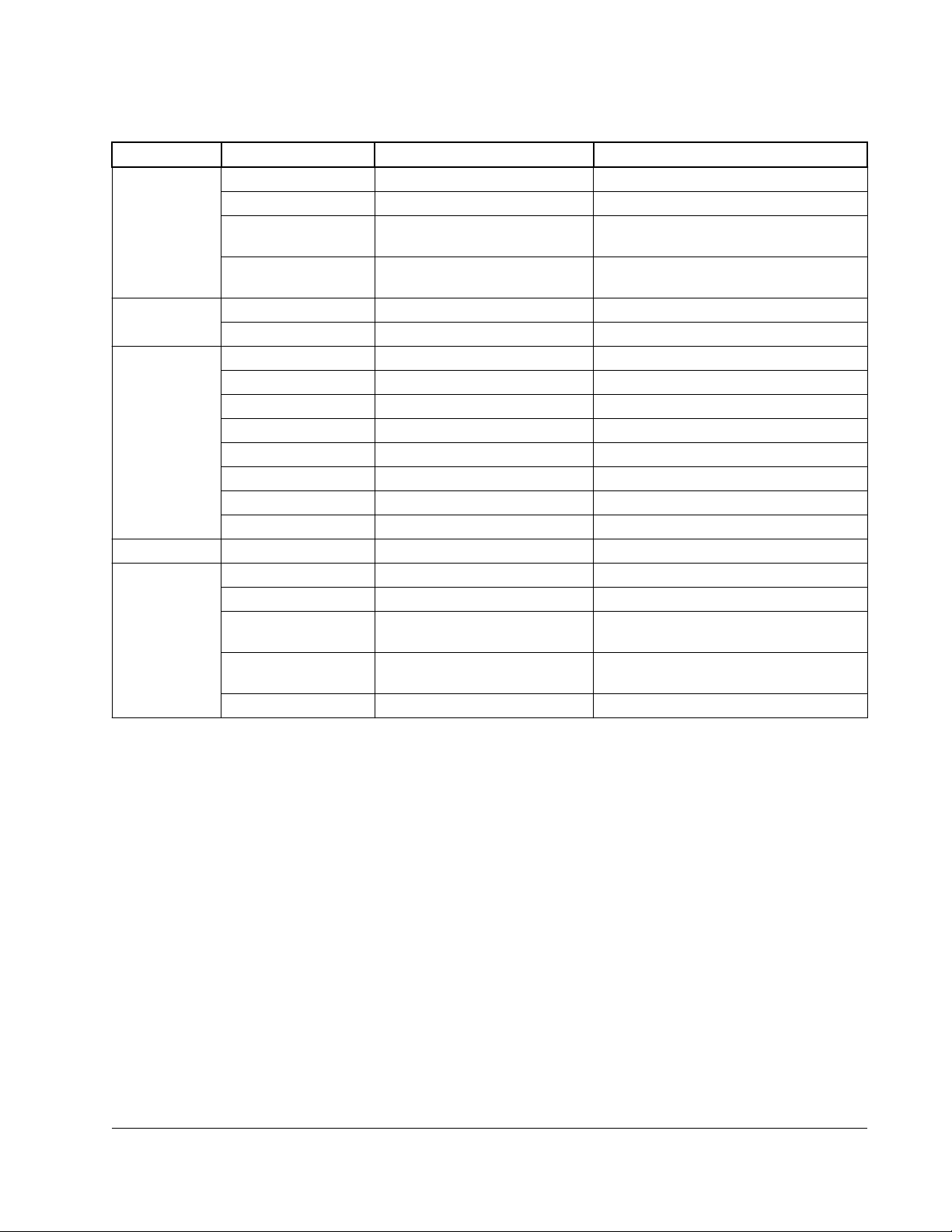
System specifications
Table 18. Required connections for unused interfaces
Module Supply Name Description Recommendations if module is unused
ADC VREFH_ANA18 High Reference supply for ADC 10 kΩ resistor to ground
VREFL_ANA Low Reference supply for ADC 10 kΩ resistor to ground
VDD_ANA18 1.8 V supply for ADC Analog and
IO segment
VDD_ANA33 3.3 V supply for ADC Analog and
IO segment
DAC DAC0_OUT DAC0 output Leave unconnected
DAC1_OUT DAC1 output Leave unconnected
MIPI DSI VDD_DSI11 MIPI 1.1 V supply 10 kΩ resistor to ground
VDD_DSI18 MIPI 1.8 V supply 10 kΩ resistor to ground
DSI_CLK_N MIPI Negative Clock Signal Leave unconnected
DSI_CLK_P MIPI Positive Clock Signal Leave unconnected
DSI_DATA0_N MIPI Negative Data0 Signal Leave unconnected
DSI_DATA0_P MIPI Positive Data0 Signal Leave unconnected
DSI_DATA1_N MIPI Negative Data1 Signal Leave unconnected
DSI_DATA1_P MIPI Positive Data1 Signal Leave unconnected
Port D Signals VDD_PTD Port D supply 10 kΩ resistor to ground
USB0 VDD_USB33 USB0 PHY 3.3 V supply 10 kΩ resistor to ground
VDD_USB18 USB0 PHY 1.8 V supply 10 kΩ resistor to ground
USB0_DM USB D- Analog Data Signal on
the USB Bus
USB0_DP USB D+ Analog Data Signal on
the USB Bus
USB0_VBUS_DETECT USB0 VBUS Detect 10 kΩ resistor to ground
10 kΩ resistor to ground
10 kΩ resistor to ground
Leave unconnected
Leave unconnected
7.5 Electrical Characteristics and Thermal Specifications
7.5.1 AC electrical characteristics
Unless otherwise specified, propagation delays are measured from the 50% to the 50%
point, and rise and fall times are measured at the 20% and 80% points, as shown in the
following figure.
i.MX 7ULP Applications Processor—Consumer, Rev. 0, 09/2020
NXP Semiconductors
51
Page 52
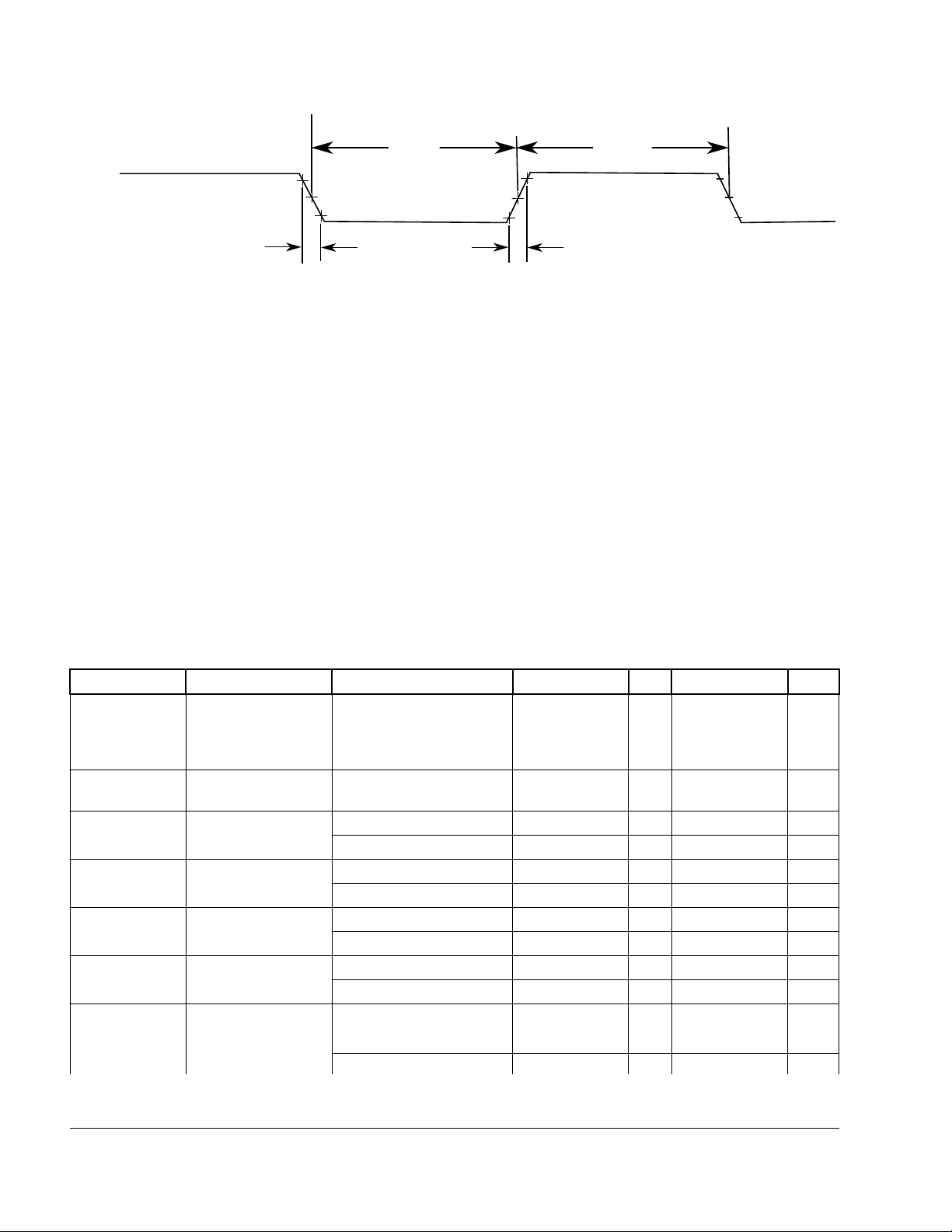
80%
20%
50%
V
IL
Input Signal
V
IH
Fall Time
High
Low
Rise Time
Midpoint1
The midpoint is VIL + (VIH - VIL) / 2
System specifications
Figure 4. Input signal measurement reference
All digital I/O switching characteristics, unless otherwise specified, assume all output
signals:
• have CL=30pF loads,
• are slew rate disabled, and
• are normal drive strength
7.5.2 Nonswitching electrical characteristics
7.5.2.1 GPIO DC Electrical Requirements
V
tol
I
tol
V
ih
V
il
DeltaV Input Hysterisis VDD_PTx = 1.72 - 1.95 V 0.15 V
I
ih
I
il
52
NXP Semiconductors
Table 19. GPIO DC Electrical Requirements
Symbol Parameter Condition Min Typ Max Unit
Fail-safe I/O tolerance
when pad supply is off
(PTA, PTB, PTC, PTE
and PTF)
I/O current when pad
supply is off
Input High VDD_PTx= 1.72 - 1.95 V 0.7*VDD_PTx V
Input Low VDD_PTx = 1.72 - 1.95 V -0.3 0.3*VDD_PTx V
High level input
current
Low level input
current
VDD_PTx=0 3.6 V
VDD_PTx=0 or floating 1 µA
VDD_PTx = 2.7 - 3.6 V 0.7*VDD_PTx V
VDD_PTx = 2.7 - 3.6 V -0.3 0.7 V
VDD_PTx = 2.7 - 3.6 V 0.15 V
VDD_PTx = 1.72 - 1.95 V -1 0.5 1 µA
VDD_PTx = 2.7 - 3.6 V -1 0.5 1 µA
VDD_PTx = 1.72 - 1.95 V
Vin = VSS
VDD_PTx = 2.7 - 3.6 V -1 1 µA
Table continues on the next page...
-1 1 µA
i.MX 7ULP Applications Processor—Consumer, Rev. 0, 09/2020
Page 53

System specifications
Table 19. GPIO DC Electrical Requirements (continued)
Symbol Parameter Condition Min Typ Max Unit
Vin = VSS
Voh (Low Drive) High Level Output
Voltage
Voh (High Drive) High Level Output
Voltage
Vol (Low Drive) Low Level Output
Voltage
Vol (High Drive) Low Level Output
Voltage
I
oz
Output Hi-Z current -5 5 µA
VDD_PTx = 1.72 - 1.95 V
Ioh = -2.9mA
VDD_PTx = 2.7 - 3.6 V
Ioh = -4mA
VDD_PTx = 1.72 - 1.95 V
Ioh = -5.8mA
VDD_PTx = 2.7 - 3.6 V
Ioh = -8mA
VDD_PTx = 1.72 - 1.95 V
Ioh = 2.9mA
VDD_PTx = 2.7 - 3.6 V
Ioh = 4mA
VDD_PTx = 1.72 - 1.95 V
Ioh = 5.8mA
VDD_PTx = 2.7 - 3.6 V
Ioh = 8mA
0.8*VDD_PTx V
0.8*VDD_PTx V
0.8*VDD_PTx V
0.8*VDD_PTx V
0.2*VDD_PTx V
0.2*VDD_PTx V
0.2*VDD_PTx V
0.2*VDD_PTx V
7.5.2.1.1 GPIO Pull-up and Pull-Down Resistance
Table 20. Failsafe GPIO (FSGPIO) pull-up and pull-down resistance (PTA, PTB, PTC, PTE
and PTF)
Symbol Parameter Min Max Unit
R Pull up Pull-up resistance 25 50 kΩ
R Pull down Pulldown resistance 25 50 kΩ
Table 21. Standard GPIO (STGPIO) pull-up and pull-down resistance (PTD)
Symbol Parameter Min Max Unit
R Pull up Pull-up resistance, high voltage range (2.7 V – 3.6 V) 10 100 kΩ
Pull-up resistance, Low voltage range (1.71 V – 1.89 V) 20 50 kΩ
R Pull down Pull-down resistance, High voltage range (2.7 V – 3.6 V) 10 100 kΩ
Pull-down resistance, Low voltage range (1.71 V – 1.89 V) 20 50 kΩ
i.MX 7ULP Applications Processor—Consumer, Rev. 0, 09/2020
53
NXP Semiconductors
Page 54
System specifications
7.5.2.2 Capacitance attributes
See the device IBIS model for pin capacitance values for the package being used.
7.5.3 Switching electrical characteristics
7.5.3.1 General switching timing specifications
These general purpose specifications apply to all signals configured for GPIO, UART,
and timer functions.
Table 22. General switching timing specifications
Symbol Parameter Min Typ Max Unit Notes
tw_GPIO_sync GPIO pin interrupt pulse width (Digital Filter
disabled) — Synchronous path
tw_RESET_async External RESET and NMI pin interrupt pulse width
— Asynchronous path
tw_GPIO_async GPIO pin interrupt pulse width — Asynchronous
path
1.5 ─ ─ Bus clock
cycles
30 ─ ─ ns 2
30 ─ ─ ns 2
1
1. The greater synchronous and asynchronous timing must be met.
2. This is the shortest pulse that is guaranteed to be recognized.
7.5.3.2 GPIO rise and fall times
Table 23. FSGPIO rise and fall time (PTA, PTB, PTC, PTE, and PTF)
Symbol Parameter Condition Min Typ Max Unit Notes
τrf transition
time
τrf transition
time
τrf transition
time
τrf transition
time
Continuous Voltage
Range Normal
VDD_PTx = 2.7–3.6 V
Continuous Voltage
Range Derated
VDD_PTx = 1.98–2.7V
Continuous Voltage
Range Derated
VDD_PTx = 1.71–1.98V
High Voltage Range
VDD_PTx = 3–3.6 V
CL = 25pF Slow Slew
Rate
Standard Slew
Rate
CL = 25pF Slow Slew
Rate
Standard Slew
Rate
CL = 25pF Slow Slew
Rate
Standard Slew
Rate
CL = 25pF Slow Slew
Rate
Standard Slew
Rate
8.3 ns 1
3.4 ns
7.3 ns
0.9 ns
5.4 ns
0.8 ns
8.3 ns
3.4 ns
54
NXP Semiconductors
Table continues on the next page...
i.MX 7ULP Applications Processor—Consumer, Rev. 0, 09/2020
Page 55

System specifications
Table 23. FSGPIO rise and fall time (PTA, PTB, PTC, PTE, and PTF) (continued)
Symbol Parameter Condition Min Typ Max Unit Notes
τrf transition
time
1. VDD1P8 = 1.8V
Low Voltage Range
VDD_PTx = 1.71–1.98 V
CL = 25pF Slow Slew
Rate
Standard Slew
Rate
5.5 ns
0.7 ns
Table 24. STGPIO rise and fall time (PTD)
Symbol Parameter Condition Min Typ Max Unit Notes
τrf transition
time
τrf transition
time
High Voltage Range
VDD_PTx = 3–3.6 Volts
Low Voltage Range
VDD_PTx = 1.71–1.98
Volts
CL = 25pF Slow Slew Rate 12.0 ns 1
Standard Slew
Rate
CL = 25pF Slow Slew Rate 7.4 ns
Standard Slew
Rate
4.1 ns
0.8 ns
1. VDD1P8 = 1.8V
7.5.3.3 GPIO output buffer maximum frequency
Table 25. GPIO output buffer maximum frequency
Symbol Parameter Condition Min Max Unit
Mfreq (low drive low slew) Maximum
Frequency
Mfreq (low drive high slew) Maximum
Frequency
Mfreq (high drive low slew) Maximum
Frequency
VDD_PTx = 1.65 - 1.95 V, CL = 5pf — 120 MHz
VDD_PTx = 1.65 - 1.95 V, CL = 10pf — 100 MHz
VDD_PTx = 1.65 - 1.95 V, CL = 40pf — 50 MHz
VDD_PTx = 2.7 - 3.6 V, CL = 5pf — 115 MHz
VDD_PTx = 2.7 - 3.6 V, CL = 10pf — 95 MHz
VDD_PTx = 2.7 - 3.6 V, CL = 40pf — 40 MHz
VDD_PTx = 1.65 - 1.95 V, CL = 5pf — 185 MHz
VDD_PTx = 1.65 - 1.95 V, CL = 10pf — 145 MHz
VDD_PTx = 1.65 - 1.95 V, CL = 40pf — 50 MHz
VDD_PTx = 2.7 - 3.6 V, CL = 5pf — 170 MHz
VDD_PTx = 2.7 - 3.6 V, CL = 10pf — 130 MHz
VDD_PTx = 2.7 - 3.6 V, CL = 40pf — 40 MHz
VDD_PTx = 1.65 - 1.95 V, CL = 5pf — 140 MHz
VDD_PTx = 1.65 - 1.95 V, CL = 10pf — 125 MHz
VDD_PTx = 1.65 - 1.95 V, CL = 40pf — 85 MHz
VDD_PTx = 2.7 - 3.6 V, CL = 5pf — 130 MHz
VDD_PTx = 2.7 - 3.6 V, CL = 10pf — 115 MHz
VDD_PTx = 2.7 - 3.6 V, CL = 40pf — 70 MHz
Table continues on the next page...
i.MX 7ULP Applications Processor—Consumer, Rev. 0, 09/2020
55
NXP Semiconductors
Page 56
System specifications
Table 25. GPIO output buffer maximum frequency (continued)
Symbol Parameter Condition Min Max Unit
Mfreq (high drive high slew) Maximum
Frequency
VDD_PTx = 1.65 - 1.95 V, CL = 5pf — 235 MHz
VDD_PTx = 1.65 - 1.95 V, CL = 10pf — 200 MHz
VDD_PTx = 1.65 - 1.95 V, CL = 40pf — 100 MHz
VDD_PTx = 2.7 - 3.6 V, CL = 5pf — 215 MHz
VDD_PTx = 2.7 - 3.6 V, CL = 10pf — 185 MHz
VDD_PTx = 2.7 - 3.6 V, CL = 40pf — 80 MHz
7.5.4 Debug and trace modules
7.5.4.1 JTAG timing specifications
Table 26. JTAG timing specifications
Symbol Parameter Min Max Min—
VLPR
mode
J1 TCLK frequency of operation
• Boundary Scan 0 10 0 10 MHz
• JTAG 0 25 0 10 MHz
J2 TCLK cycle period 1000/J1 — 1000/J1 — ns
J3 TCLK clock pulse width
• Boundary Scan 50 — 50 — ns
• JTAG 20 — 20 — ns
J4 TCLK rise and fall times — 3 — 3 ns
J5 Boundary scan input data setup time to TCLK
rise
J6 Boundary scan input data hold time after TCLK
rise
J7 TCLK low to boundary scan output data valid — 28 — 28 ns
J8 TCLK low to boundary scan output high-Z — 25 — 25 ns
J9 TMS, TDI input data setup time to TCLK rise 10.5 — 19 — ns
J10 TMS, TDI input data hold time after TCLK rise 2.5 — 2 — ns
J11 TCLK low to TDO data valid — 19 — 19 ns
J12 TCLK low to TDO high-Z 2 — 2 — ns
J13 TRST assert time 100 — 100 — ns
J14 TRST setup time (negation) to TCLK high 8 — 8 — ns
20 — 20 — ns
5 — 5 — ns
Max—
VLPR
mode
Unit
56
NXP Semiconductors
i.MX 7ULP Applications Processor—Consumer, Rev. 0, 09/2020
Page 57

J2
J3 J3
J4 J4
TCLK (input)
Figure 5. Test clock input timing
J7
J8
J7
J5
J6
Input data valid
Output data valid
Output data valid
TCLK
Data inputs
Data outputs
Data outputs
Data outputs
System specifications
Figure 6. Boundary scan (JTAG) timing
i.MX 7ULP Applications Processor—Consumer, Rev. 0, 09/2020
57
NXP Semiconductors
Page 58

J11
J12
J11
J9
J10
Input data valid
Output data valid
Output data valid
TCLK
TDI/TMS
TDO
TDO
TDO
J14
J13
TCLK
TRST
System specifications
Figure 7. Test Access Port timing
Figure 8. TRST timing
7.5.4.2
Serial Wire Debug (SWD) timing specifications
Table 27. SWD timing specificaions
Symbol Description Min Max Min—
J1 SWD_CLK frequency of operation
J2 SWD_CLK cycle period 1000/J1 — 1000/J1 — ns
J3 SWD_CLK clock pulse width
J4 SWD_CLK rise and fall times — 3 — 3 ns
J9 SWD_DIO input data setup time to SWD_CLK
rise
58
NXP Semiconductors
Table continues on the next page...
0 25 0 10 MHz
20 — 20 — ns
10 — 19 — ns
i.MX 7ULP Applications Processor—Consumer, Rev. 0, 09/2020
VLPR
mode
Max—
VLPR
mode
Unit
Page 59
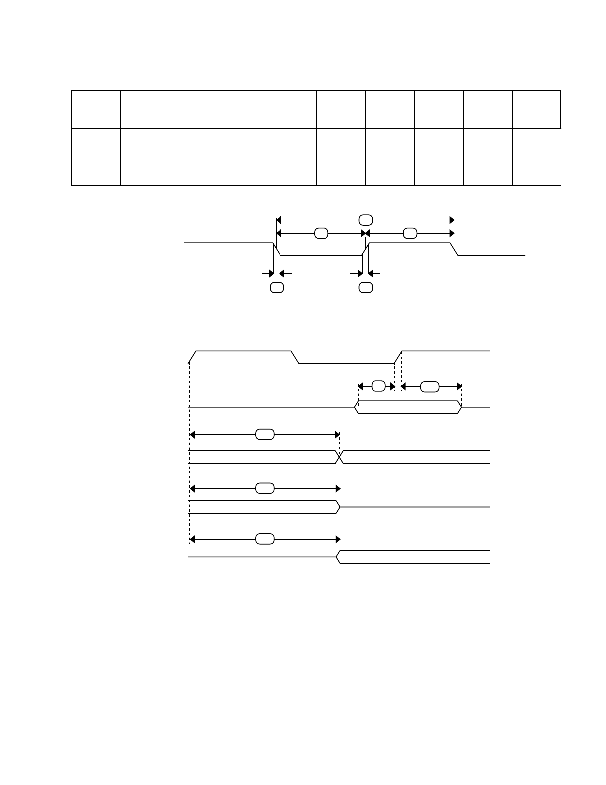
Table 27. SWD timing specificaions (continued)
J2
J3 J3
J4 J4
SWD_CLK (input)
J11
J12
J11
J9
J10
Input data valid
Output data valid
Output data valid
SWD_CLK
SWD_DIO
SWD_DIO
SWD_DIO
SWD_DIO
System specifications
Symbol Description Min Max Min—
VLPR
mode
J10 SWD_DIO input data hold time after SWD_CLK
rise
J11 SWD_CLK high to SWD_DIO data valid — 37 — 37 ns
J12 SWD_CLK high to SWD_DIO high-Z 2 — 2 — ns
0 — 0 — ns
Max—
VLPR
mode
Figure 9. SWD clock input timing
Unit
7.5.5
i.MX 7ULP Applications Processor—Consumer, Rev. 0, 09/2020
Thermal specifications
Figure 10. SWD data timing
59
NXP Semiconductors
Page 60

System specifications
7.5.5.1 Thermal operating requirements
Table 28. Thermal operating requirements
Symbol Parameter Min. Typ Max. Unit
T
Die junction temperature—Commercial 0 – 95 °C
J
7.5.5.2 Thermal attributes
NOTE
Per JEDEC JESD51-2, the intent of thermal resistance
measurements is solely for a thermal performance comparison
of one package to another in a standardized environment. This
methodology is not meant to and does not predict the
performance of a package in an application-specific
environment.
Table 29. Thermal resistance data
Rating Test Conditions Symbol 14x14 mm
(VK) Package
Value
Junction to Ambient
Natural Convection
Junction to Ambient
Natural Convection
Junction to Ambient (@
200 ft/min)
Junction to Ambient (@
200 ft/min)
Junction to Board ─ RθJB 15.6 24.2 °C/W 4
Junction to Case ─ RθJC 11.7 11.4 °C/W 5
Junction to Package
Top
Junction to Package
Bottom
1. Junction temperature is a function of die size, on-chip power dissipation, package thermal resistance, mounting site
(board) temperature, ambient temperature, air flow, power dissipation of the other components on the board, and board
thermal resistance.
2. Per SEMI G38-87 and JEDEC JESD51-2 with the single layer board horizontal.
3. Per JEDEC JESD51-6 with the board horizontal.
4. Thermal resistance between the die and the printed circuit board per JEDEC JESD51-8. Board temperature is measured
on the top surface of the board near the package.
5. Thermal resistance between the die and the case top surface as measured by the cold plate method (MIL SPEC-883).
6. Thermal characterization parameter indicating the temperature difference between package top and the junction
temperature per JEDEC JESD51-2. When Greek letters are not available, the thermal characterization parameter is
written as ΨJT.
Single-layer board
(1S)
Four-layer board
(2s2p)
Single-layer board
(1S)
Four-layer board
(2s2p)
Natural Convection ΨJT 0.4 0.2 °C/W 6
Natural Convection ΨJB 10.1 17.4 °C/W 7
RθJA 49.5 71.2 °C/W 1,2
RθJA 30.7 41.4 °C/W 1,2,3
RθJMA 38.6 56.4 °C/W 1,3
RθJMA 26.0 36.7 °C/W 1,3
10x10 mm (VP)
Package Value
Unit Notes
60
NXP Semiconductors
i.MX 7ULP Applications Processor—Consumer, Rev. 0, 09/2020
Page 61

Specifications—application domain
7. Thermal resistance between the die and the central solder balls on the bottom of the package based on simulation.
8 Specifications—application domain
8.1 Peripheral operating requirements and behaviors
8.1.1 DDR timing—application domain
See Multi Mode DDR Controller (MMDC).
8.1.2 Ultra-high-speed SD/SDIO/MMC host interface (uSDHC) AC timing—application domain
This section describes the electrical information of the uSDHC, which includes
support for eMMC and SD (Secure Digital) interfaces.
eMMC is designed to be compliant with the eMMC specification 5.0 and supports the
following modes:
• Backward Compatibility mode (MMC)
• High Speed mode
• HS200
• HS400
The SD (Secure Digital) interface is designed to be compliant with the SD 3.0
specification and supports the following operating modes:
• SDR12
• SDR25
• SDR50
• SDR104
• DDR50
8.1.2.1
SD/eMMC4.3 (single data rate) AC timing
The following figure shows the AC timing of SD/eMMC4.3, and the table lists the
SD/eMMC4.3 timing characteristics.
i.MX 7ULP Applications Processor—Consumer, Rev. 0, 09/2020
NXP Semiconductors
61
Page 62

Specifications—application domain
Figure 11. SD/eMMC4.3 AC timing
Table 30. SD/eMMC4.3 AC parameters
ID Parameter Symbols Min Max Unit
Card Input Clock
SD1 Clock Frequency (Low Speed) f
Clock Frequency (SD/SDIO Full
Speed/High Speed)
Clock Frequency (MMC Full
Speed/High Speed)
Clock Frequency (Identification
Mode)
SD2 Clock Low Time t
SD3 Clock High Time t
SD4 Clock Rise Time t
SD5 Clock Fall Time t
uSDHC Output/Card Inputs SD_CMD, SDx_DATAx (Reference to CLK)
SD6 uSDHC Output Delay t
uSDHC Input/Card Outputs SD_CMD, SDx_DATAx (Reference to CLK)
SD7 uSDHC Input Setup Time t
SD8 uSDHC Input Hold Time
4
PP
f
PP
f
PP
f
TLH
THL
OD
WL
WH
OD
ISU
t
IH
1
2
3
0 400 kHz
0 25/50 MHz
0 20/52 MHz
100 400 kHz
7 — ns
7 — ns
— 3 ns
— 3 ns
-3.3 3.6 ns
7.5 — ns
1.0 — ns
1. In Low-Speed mode, card clock must be lower than 400 kHz, voltage ranges from 2.7 to 3.6 V.
2. In Normal (Full) -Speed mode for SD/SDIO card, clock frequency can be any value between 0–25 MHz. In High-speed
mode, clock frequency can be any value between 0–50 MHz.
3. In Normal (Full) -Speed mode for MMC card, clock frequency can be any value between 0–20 MHz. In High-speed
mode, clock frequency can be any value between 0–52 MHz.
62
i.MX 7ULP Applications Processor—Consumer, Rev. 0, 09/2020
NXP Semiconductors
Page 63

Specifications—application domain
4. To satisfy hold timing, the delay difference between clock input and cmd/data input must not exceed 2 ns.
8.1.2.2 eMMC4.4/4.41 (dual data rate) AC timing
The following figure shows the timing of eMMC4.4/4.41, and the table lists the
eMMC4.4/4.41 timing characteristics. Note that only DATA is sampled on both edges
of the clock (not applicable to CMD).
Figure 12. eMMC4.4/4.41 timing
Table 31. eMMC4.4/4.41 interface timing specifications
ID Parameter Symbols Min Max Unit
Card Input Clock
SD1 Clock Frequency (eMMC4.4/4.41
DDR)
SD1 Clock Frequency (SD3.0 DDR) f
uSDHC Output / Card Inputs SD_CMD, SDx_DATAx (Reference to CLK)
SD2 uSDHC Output Delay t
uSDHC Input / Card Outputs SD_CMD, SDx_DATAx (Reference to CLK)
SD3 uSDHC Input Setup Time t
SD4 uSDHC Input Hold Time t
f
ISU
PP
PP
OD
IH
0 52 MHz
0 50 MHz
-3.3 3.6 ns
7.3 — ns
1.0 — ns
8.1.2.3 HS200 mode timing
The following figure depicts the timing of HS200 mode, and the subsequent table lists
the HS200 timing characteristics.
i.MX 7ULP Applications Processor—Consumer, Rev. 0, 09/2020
63
NXP Semiconductors
Page 64
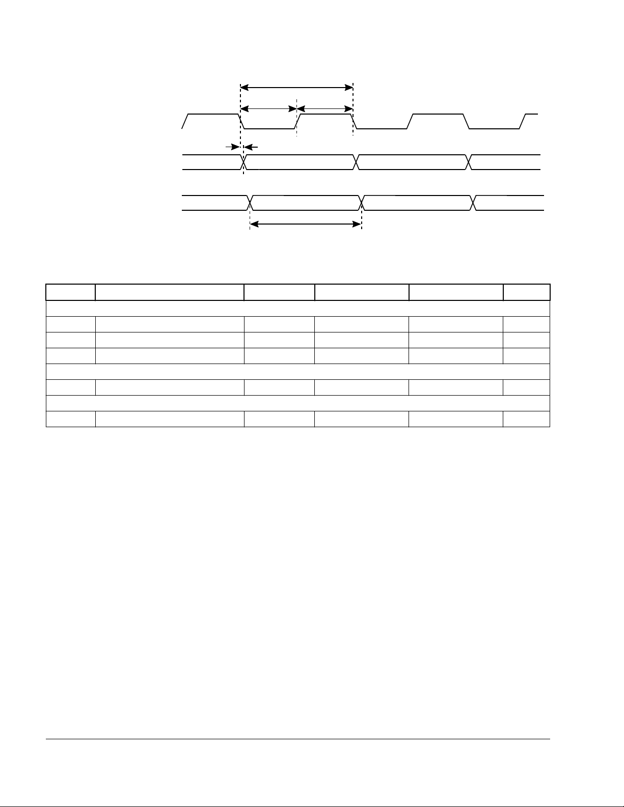
SCLK
8-bit output from uSDHC to eMMC
8-bit input from eMMC to uSDHC
'
SD3
SD1
SD2
SD4/SD5
SD8
Specifications—application domain
Figure 13. HS200 timing
Table 32. HS200 interface timing specifications
ID Parameter Symbols Min. Max. Unit
Card Input clock
SD1 Clock Frequency Period t
SD2 Clock Low Time t
SD3 Clock High Time t
uSDHC Output/Card Inputs SD_CMD, SDx_DATAx in HS200 (Reference to CLK)
SD5 uSDHC Output Delay t
uSDHC Input/Card Outputs SD_CMD, SDx_DATAx in HS200 (Reference to CLK)
SD8 Card Output Data Window t
CLK
CL
CH
OD
ODW
5.0 — ns
0.46 × t
0.46 × t
CLK
CLK
0.54 × t
0.54 × t
CLK
CLK
1
-1.6 0.74 ns
0.5 x t
CLK
— ns
ns
ns
1. HS200 is for 8 bits while SDR104 is for 4 bits
8.1.2.4 HS400 AC timing—eMMC5.0 only
The following figure depicts the timing of HS400, and the subsequent table lists the
HS400 timing characteristics. Be aware that only data is sampled on both edges of the
clock (not applicable to CMD). The CMD input/output timing for HS400 mode is the
same as CMD input/output timing for SDR104 mode. Check parameters SD5, SD6, and
SD7 in Table 34 for CMD input/output timing for HS400 mode.
64
NXP Semiconductors
i.MX 7ULP Applications Processor—Consumer, Rev. 0, 09/2020
Page 65

SD7
SD1
SD5 SD5
SD6
SCK
Output from
Strobe
Input from
uSDHC to eMMC
eMMC to uSDHC
DAT0
DAT1
DAT7
...
DAT0
DAT1
DAT7
...
SD4
SD4
SD3
SD2
Specifications—application domain
Figure 14. HS400 timing
Table 33. HS400 timing specifications
ID Parameter Symbols Min Max Unit
Card Input clock
SD1 Clock Frequency fPP 0 192 MHz
SD2 Clock Low Time tCL 0.46 × tCLK 0.54 × tCLK ns
SD3 Clock High Time tCH 0.46 × tCLK 0.54 × tCLK ns
uSDHC Output/Card inputs DAT (Reference to SCK)
SD4 Output Skew from Data of Edge of
SCK
SD5 Output Skew from Edge of SCK to
Data
uSDHC input/Card Outputs DAT (Reference to Strobe)
SD6 uSDHC input skew tRQ — 0.45 ns
SD7 uSDHC hold skew tRQH — 0.45 ns
tOSkew1 0.45 — ns
tOSkew2 0.45 — ns
8.1.2.5 SDR50/SDR104 AC timing
The following figure shows the timing of SDR50/SDR104, and the table lists the
SDR50/SDR104 timing characteristics.
i.MX 7ULP Applications Processor—Consumer, Rev. 0, 09/2020
65
NXP Semiconductors
Page 66
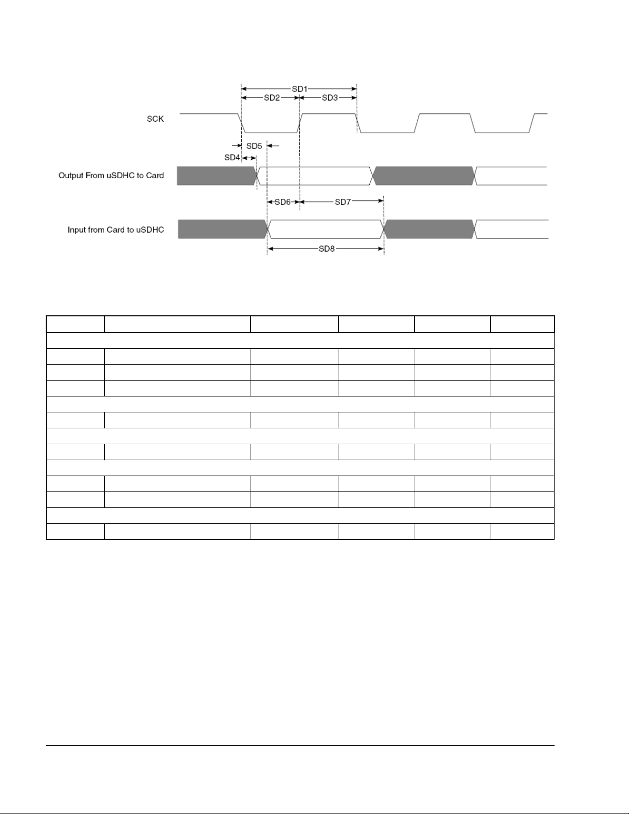
Specifications—application domain
Figure 15. SDR50/SDR104 timing
Table 34. SDR50/SDR104 interface timing specification
ID Parameter Symbols Min Max Unit
Card Input Clock
SD1 Clock Frequency Period t
SD2 Clock Low Time t
SD3 Clock High Time t
uSDHC Output/Card Inputs SD_CMD, SDx_DATAx in SDR50 (Reference to CLK)
SD4 uSDHC Output Delay t
uSDHC Output/Card Inputs SD_CMD, SDx_DATAx in SDR104 (Reference to CLK)
SD5 uSDHC Output Delay t
uSDHC Input/Card Outputs SD_CMD, SDx_DATAx in SDR50 (Reference to CLK)
SD6 uSDHC Input Setup Time t
SD7 uSDHC Input Hold Time t
uSDHC Input/Card Outputs SD_CMD, SDx_DATAx in SDR104 (Reference to CLK)
SD8 Card Output Data Window t
CLK
CL
CH
OD
OD
ISU
IH
ODW
4.8 — ns
0.46*t
0.46*t
CLK
CLK
0.54*
0.54*t
CLK
CLK
-3 1 ns
-1.6 0.74 ns
2.5 — ns
1.5 — ns
1
0.5*t
CLK
— ns
ns
ns
1. Data window in SDR100 mode is variable.
8.1.2.6 Bus operation condition for 3.3 V and 1.8 V signaling
Signaling level of SD/eMMC4.3 and eMMC4.4/4.41 modes is 3.3 V. Signaling level of
SDR104/SDR50 mode is 1.8 V.
66
NXP Semiconductors
i.MX 7ULP Applications Processor—Consumer, Rev. 0, 09/2020
Page 67
Specifications—application domain
8.1.3 Flexbus switching specifications
All processor bus timings are synchronous; input setup/hold and output delay are
given in respect to the rising edge of a reference clock, FB_CLK. The FB_CLK
frequency may be the same as the internal system bus frequency or an integer divider
of that frequency.
The following timing parameters indicate when data is latched or driven onto the
external bus, relative to the Flexbus output clock (FB_CLK). All other timing
relationships can be derived from these values.
Table 35. Flexbus switching specifications
Num Parameter Min. Max. Unit Notes
Frequency of operation
• HSRUN mode
• Normal RUN mode
FB1 Clock period
• HSRUN mode
• Normal RUN mode
FB2 Address, data, and control output valid — 13.0 ns 1
FB3 Address, data, and control output hold 1.0 — ns 1
FB4 Data input setup 8.5 — ns 2
FB5 Data input hold 0.0 — ns 2
—
15.0
15.0
66
66
— ns
MHz
1. Specification is valid for all FB_AD[31:0], FB_BE, FB_CSn_B, FB_OE_B, FB_RW_B, FB_TBST_B, FB_TSIZ[1:0],
FB_ALE, and FB_TS_B.
2. Specification is valid for all FB_AD[31:0].
i.MX 7ULP Applications Processor—Consumer, Rev. 0, 09/2020
67
NXP Semiconductors
Page 68
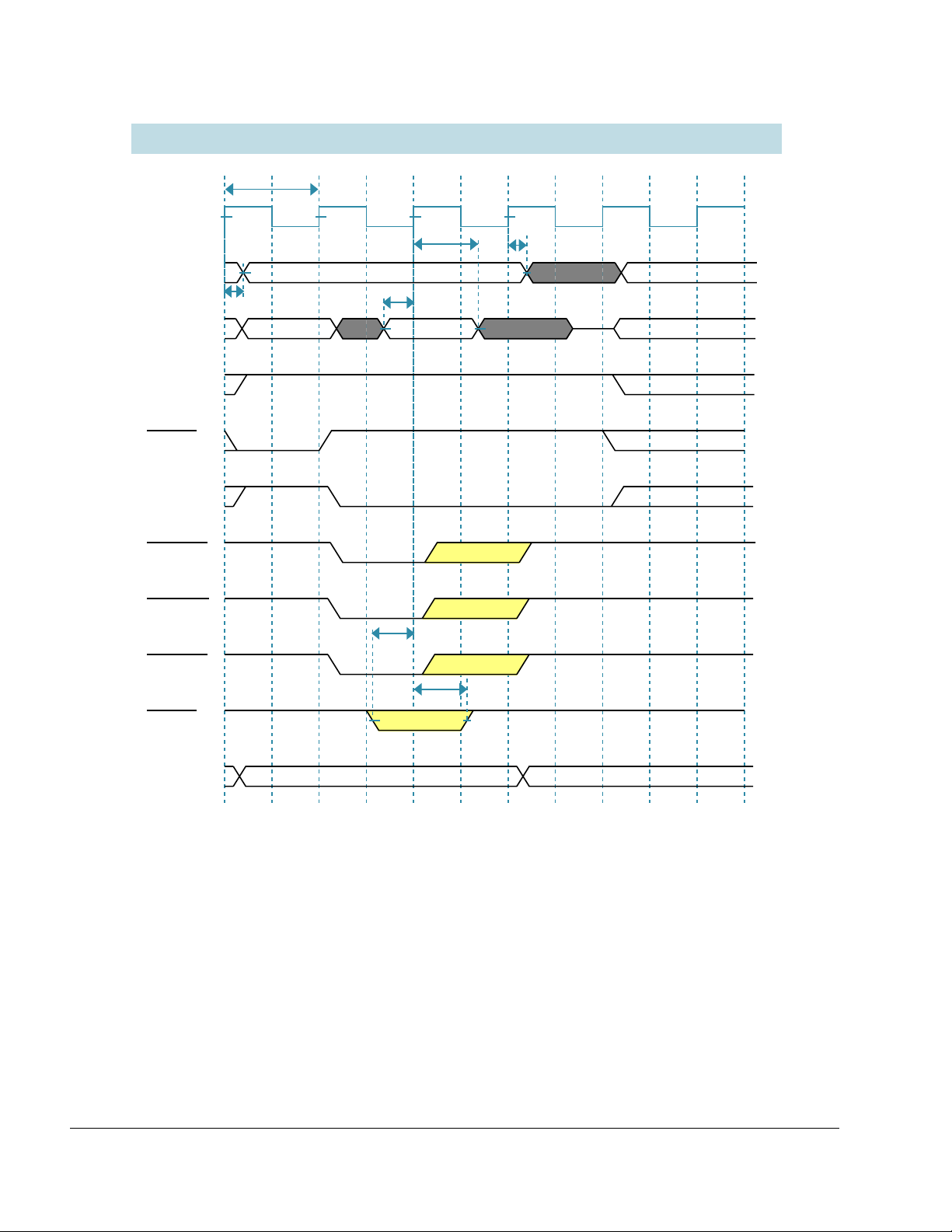
Address
Address Data
TSIZ
AA=1
AA=0
AA=1
AA=0
FB3
FB5
FB4
FB4
FB5
FB1
FB_CLK
FB_A[Y]
FB_D[X]
FB_RW
FB_TS
FB_ALE
FB_CSn
FB_OEn
FB_BEn
FB_TA
FB_TSIZ[1:0]
FB2
Read Timing Parameters
electricals_read.svg
S0 S1 S2 S3 S0
S0 S1 S2 S3 S0
Specifications—application domain
Figure 16. FlexBus read timing diagram
NOTE
The Transfer Acknowledge Signal (FB_TA) is hard-wired in
the design of i.MX 7ULP, so this signal is not available.
68
NXP Semiconductors
i.MX 7ULP Applications Processor—Consumer, Rev. 0, 09/2020
Page 69
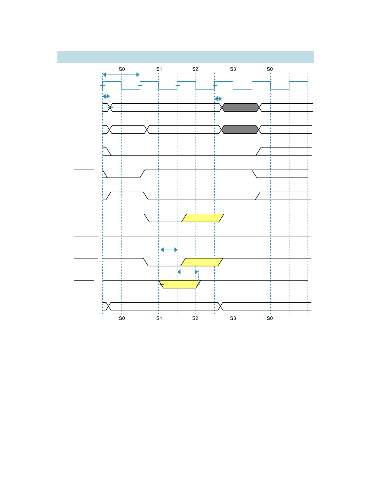
Address
Address Data
TSIZ
AA=1
AA=0
AA=1
AA=0
FB1
FB3
FB4
FB5
FB2
FB_CLK
FB_A[Y]
FB_D[X]
FB_RW
FB_TS
FB_ALE
FB_CSn
FB_OEn
FB_BEn
FB_TA
FB_TSIZ[1:0]
Write Timing Parameters
electricals_write.svg
Specifications—application domain
The Transfer Acknowledge Signal (FB_TA) is hard-wired in
the design of i.MX 7ULP, so this signal is not available.
Figure 17. FlexBus write timing diagram
NOTE
8.1.4
i.MX 7ULP Applications Processor—Consumer, Rev. 0, 09/2020
Display, Video, and Audio Interfaces
69
NXP Semiconductors
Page 70
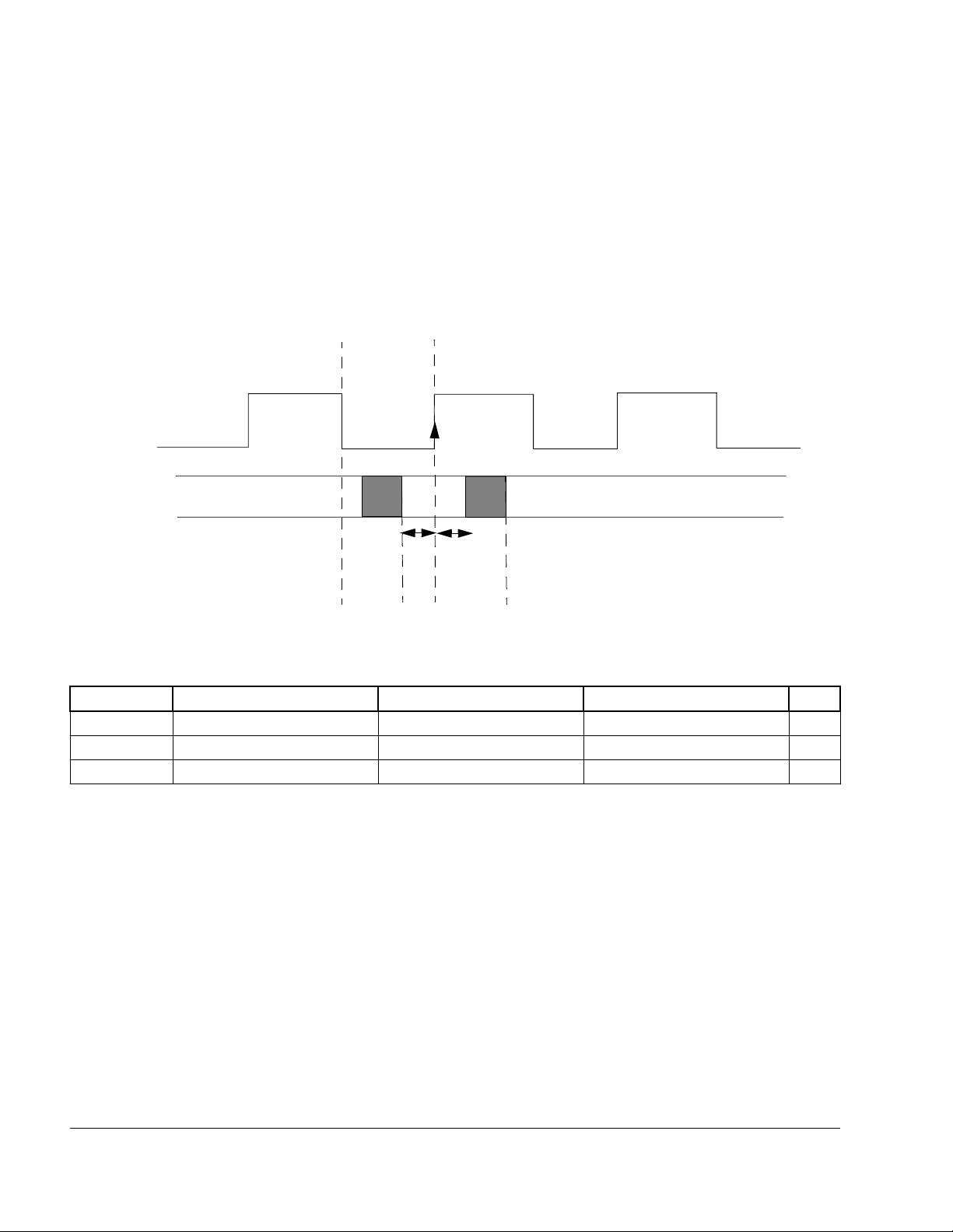
t
HO
t
SU
VIU_PCLK
VIU_D[23:0]
Specifications—application domain
8.1.4.1 MIPI DSI timing—application domain
The i.MX 7ULP conforms to the MIPI D-PHY electrical specifications MIPI DSI
Version 1.01 and D-PHY specification Rev. 1.0 (and also DPI version 2.0, DBI version
2.0, DSC version 1.0a at protocol layer) for MIPI display port x2 lanes.
8.1.4.2 Video Input Unit timing
This section provides the timing parameters of the Video Input Unit (VIU) interface.
Figure 18. VIU Timing Parameters
Table 36. VIU Timing Parameters
Symbol Characteristic Min Max Unit
f
PIX_CK
t
DSU
t
DHD
VIU pixel clock frequency _ 66.7 MHz
VIU data setup time 9.0 _ ns
VIU data hold time 1 _ ns
8.1.5 Timer specifications—application domain
See General switching timing specifications for EWM, LPTMR, and TPM.
8.1.6
Connectivity and communications specifications—application domain
70
NXP Semiconductors
i.MX 7ULP Applications Processor—Consumer, Rev. 0, 09/2020
Page 71
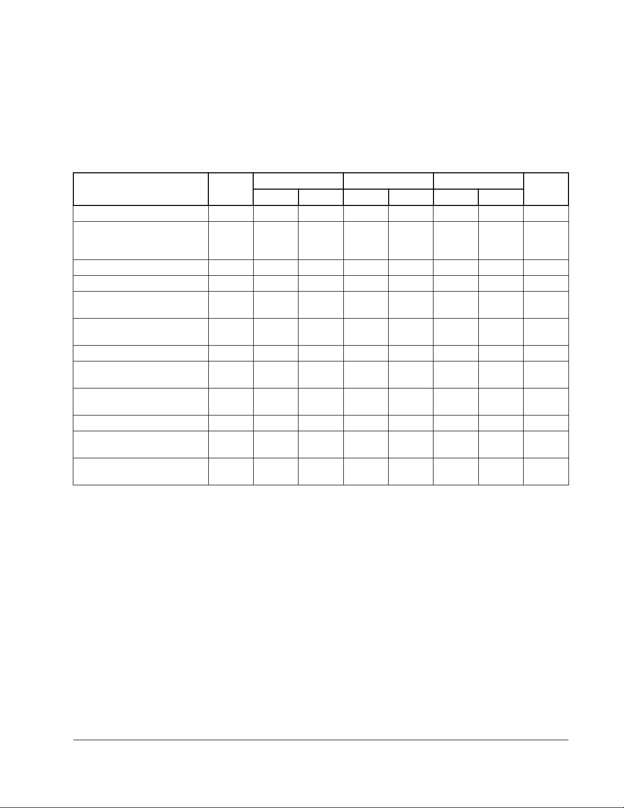
Specifications—application domain
8.1.6.1 LPUART
See General switching timing specifications.
8.1.6.2 Inter-Integrated Circuit Interface (I2C) timing
Table 37. I 2C timing (Standard, Fast, and Fast Plus modes)
Parameter Symbol Standard Mode Fast Mode Fast-mode Plus Unit
Min Max Min Max Min Max
SCL Clock Frequency f
Hold time (repeated) START
SCL
tHD; STA 4 — 0.6 — 0.26 — µs
condition. After this period, the
first clock pulse is generated.
LOW period of the SCL clock t
HIGH period of the SCL clock t
Set-up time for a repeated
LOW
HIGH
tSU; STA 4.7 — 0.6 — 0.26 — µs
START condition
Data hold time for I2C bus
tHD; DAT 0
devices
Data set-up time tSU; DAT 250
Rise time of SDA and SCL
t
r
signals
Fall time of SDA and SCL
t
f
signals
Set-up time for STOP condition tSU; STO 4 — 0.6 — 0.26 — µs
Bus free time between STOP
t
BUF
and START condition
Pulse width of spikes that must
t
SP
be suppressed by the input filter
0 100 0 400 0 1000 kHz
4.7 — 1.3 — 0.5 — µs
4 — 0.6 — 0.26 — µs
1
4
— 1000 20
— 300 20
2
3.45
— 100
3
0
+0.1C
+0.1C
2, 5
6
b
5
b
1
0.9
0 — µs
— 50 — ns
300 20
+0.1C
300 20
+0.1C
7
b
5
b
120 ns
120 ns
4.7 — 1.3 — 0.5 — µs
N/A N/A 0 50 0 50 ns
1. The master mode I2C deasserts ACK of an address byte simultaneously with the falling edge of SCL. If no slaves
acknowledge this address byte, then a negative hold time can result, depending on the edge rates of the SDA and
SCL lines.
2. The maximum tHD; DAT must be met only if the device does not stretch the LOW period (tLOW) of the SCL signal.
3. Input signal Slew = 10 ns and Output Load = 50 pF
4. Set-up time in slave-transmitter mode is 1 IPBus clock period, if the TX FIFO is empty.
5. A Fast mode I2C bus device can be used in a Standard mode I2C bus system, but the requirement t
SU; DAT
≥ 250 ns
must then be met. This is automatically the case if the device does not stretch the LOW period of the SCL signal. If
such a device does stretch the LOW period of the SCL signal, then it must output the next data bit to the SDA line t
+ t
= 1000 + 250 = 1250 ns (according to the Standard mode I2C bus specification) before the SCL line is
SU; DAT
released.
6. Cb = total capacitance of the one bus line in pF.
7. Cb = total capacitance of the one bus line in pF.
i.MX 7ULP Applications Processor—Consumer, Rev. 0, 09/2020
NXP Semiconductors
rmax
71
Page 72

SDA
HD; STA
t
HD; DAT
t
LOW
t
SU; DAT
t
HIGH
t
SU; STA
SR
P
S
S
t
HD; STA
t
SP
t
SU; STO
t
BUF
t
f
t
r
t
f
t
r
SCL
t
Specifications—application domain
Figure 19. Timing definition for standard, fast, and fast plus devices on the I2C bus
2
Table 38. I
Parameter Symbol Minimum Maximum Unit
SCLH Clock Frequency f
Hold time (repeated) START condition. After this
period, the first clock pulse is generated.
LOW period of the SCLH clock t
HIGH period of the SCLH clock t
Set-up time for a repeated START condition tSU; STA 160 — ns
Data hold time for I2C bus devices tHD; DAT 0 70 ns
Data set-up time tSU; DAT 10 — ns
Rise time of SCLH signal t
Rise time of SCLH signal after a repeated START
condition and after an acknowledge bit
Fall time of SCLH signal t
Rise time of SDAH signal t
Fall time of SDAH signal t
Set-up time for STOP condition tSU; STO 160 — ns
Pulse width of spikes that must be suppressed by
the input filter
C timing (High speed mode)
SCLH
tHD; STA 160 — ns
LOW
HIGH
rCL
t
rCL1
fCL
rDA
fDA
t
SP
0 3.4 MHz
160 — ns
60 — ns
10 40 ns
10 80 ns
10 40 ns
10 80 ns
10 80 ns
0 10 ns
8.1.6.3 Low Power Serial Peripheral Interface (LPSPI) switching specifications—application domain
The Low Power Serial Peripheral Interface (LPSPI) provides a synchronous serial bus
with master and slave operations. Many of the transfer attributes are programmable.
The following tables provide timing characteristics for classic LPSPI timing modes. See
the LPSPI chapter of the chip reference manual for information about the modified
transfer formats used for communicating with slower peripheral devices.
72
NXP Semiconductors
i.MX 7ULP Applications Processor—Consumer, Rev. 0, 09/2020
Page 73

Specifications—application domain
All timing is shown with respect to 20% VDD and 80% VDD thresholds, unless noted,
as well as input signal transitions of 3 ns and a 30 pF maximum load on all LPSPI
pins.
Table 39. LPSPI master mode switching specifications
Num. Symbol Description Min Max Unit Note
1 f
2 t
SPSCK
3 t
4 t
5 t
WSPSCK
6 t
7 t
8 t
9 t
Lead
Lag
SU
HO
Frequency of operation: MHz 1
op
LPSPI0-1 f
LPSPI2-3 f
/2048 30
periph
/2048 50
periph
SPSCK period: ns 2
LPSPI0-1 33.33 2048 x t
LPSPI2-3 16.67 2048 x t
periph
periph
Enable lead time 1/2 — t
Enable lag time 1/2 — t
Clock (SPSCK) high or low time (t
SPSCK
/2) - 2 (t
/2) + 2 ns —
SPSCK
Data setup time (inputs): — ns —
LPSPI0-1 16.0
LPSPI2-3 11.6
Data hold time (inputs) 0 — ns —
HI
Data valid (after SPSCK edge): — ns —
v
LPSPI0-1 17.2
LPSPI2-3 10.0
Data hold time (outputs) -0.7 — ns —
SPSCK
SPSCK
—
—
1. Max frequency is also limited to f
2. t
periph
= 1/f
periph
periph
/2, where f
is programmable for each LPSPIn module
periph
i.MX 7ULP Applications Processor—Consumer, Rev. 0, 09/2020
73
NXP Semiconductors
Page 74

(OUTPUT)
2
8
6 7
MSB IN2
LSB IN
MSB OUT2
LSB OUT
9
5
5
3
(CPOL=0)
4
11
11
10
10
SPSCK
SPSCK
(CPOL=1)
2. LSBF = 0. For LSBF = 1, bit order is LSB, bit 1, ..., bit 6, MSB.
1. If configured as an output.
SS
1
(OUTPUT)
(OUTPUT)
MOSI
(OUTPUT)
MISO
(INPUT)
BIT 6 . . . 1
BIT 6 . . . 1
2
6 7
MSB IN2
BIT 6 . . . 1
MASTER MSB OUT
2
MASTER LSB OUT
5
5
8
10 11
PORT DATA
PORT DATA
3
10 11 4
1.If configured as output
2. LSBF = 0. For LSBF = 1, bit order is LSB, bit 1, ..., bit 6, MSB.
9
(OUTPUT)
(CPOL=0)
SPSCK
SPSCK
(CPOL=1)
SS
1
(OUTPUT)
(OUTPUT)
MOSI
(OUTPUT)
MISO
(INPUT)
LSB IN
BIT 6 . . . 1
Specifications—application domain
Figure 20. LPSPI master mode timing (CPHA = 0)
74
NXP Semiconductors
Num. Symbol Description Min Max Unit Note
1 f
op
Figure 21. LPSPI master mode timing (CPHA = 1)
Table 40. LPSPI slave mode switching specifications
Frequency of operation: MHz 1
LPSPI0-1 0 15
LPSPI2-3 0 25
Table continues on the next page...
i.MX 7ULP Applications Processor—Consumer, Rev. 0, 09/2020
Page 75
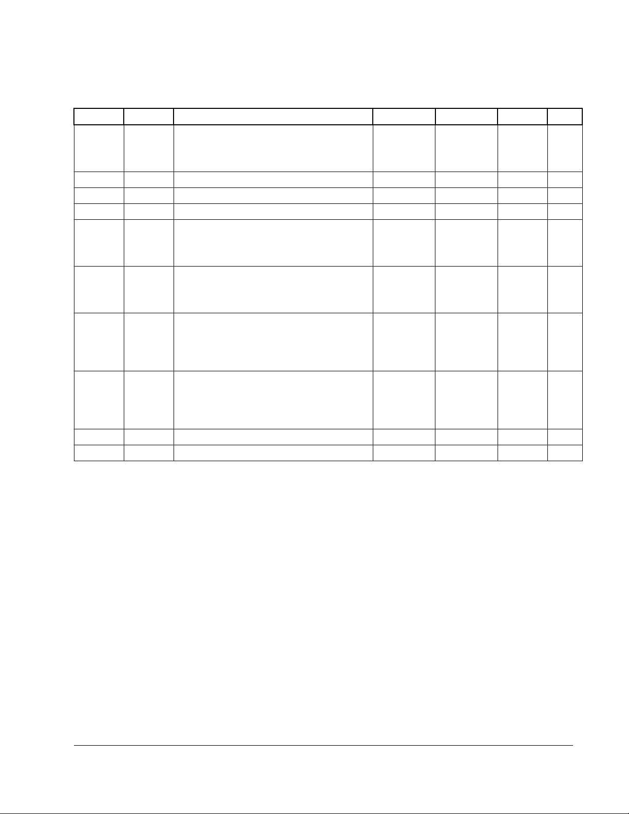
Specifications—application domain
Table 40. LPSPI slave mode switching specifications
(continued)
Num. Symbol Description Min Max Unit Note
2 t
3 t
4 t
SS2SPSCK
SPSCK2SS
5 t
6 t
7 t
8 t
9 t
SPSCK2DV
SPSCK2DH
10 t
11 t
SPSCK
WSPSCK
SS2DRV
SS2HIZ
SPSCK period: ns —
LPSPI0-1 66.6 —
LPSPI2-3 40 —
SPI_SS valid to SPI_SPSCK delay 1 — t
SPI_SPSCK to SPI_SS invalid delay 1 — t
Clock (SPSCK) high or low time (t
Data setup time (inputs): ns —
SU
SPSCK
/2) - 2 (t
/2) + 2 ns —
SPSCK
LPSPI0-1 9 —
LPSPI2-3 4.2 —
Data hold time (inputs): ns —
HI
LPSPI0-1 6 —
LPSPI2-3 3.9 —
SPI_SPSCK to SPI_MISO data valid (output
data valid):
LPSPI0-1 — 20.0
LPSPI2-3 — 15.5
SPI_SPSCK to SPI_MISO data invalid (output
data hold):
LPSPI0-1 2.0 —
LPSPI2-3 2.0 —
SPI_SS active to SPI_MISO driven 18.1 — ns —
SPI_SS inactive to SPI_MISO not driven 18 — ns —
periph
periph
ns —
ns —
2
2
1. Max frequency is also limited to f
2. t
periph
= 1/f
periph
periph
/4, where f
is programmable for each LPSPIn module
periph
i.MX 7ULP Applications Processor—Consumer, Rev. 0, 09/2020
75
NXP Semiconductors
Page 76

2
10
6 7
MSB IN
BIT 6 . . . 1
SLAVE MSB
SLAVE LSB OUT
11
5
5
3
8
4
13
NOTE: Not defined
12
12
11
SEE
NOTE
13
9
see
note
(INPUT)
(CPOL=0)
SPSCK
SPSCK
(CPOL=1)
SS
(INPUT)
(INPUT)
MOSI
(INPUT)
MISO
(OUTPUT)
LSB IN
BIT 6 . . . 1
2
6 7
MSB IN
BIT 6 . . . 1
MSB OUT SLAVE LSB OUT
5
5
10
12 13
3
12 13
4
SLAVE
8
9
see
note
(INPUT)
(CPOL=0)
SPSCK
SPSCK
(CPOL=1)
SS
(INPUT)
(INPUT)
MOSI
(INPUT)
MISO
(OUTPUT)
NOTE: Not defined
11
LSB IN
BIT 6 . . . 1
Specifications—application domain
Figure 22. LPSPI slave mode timing (CPHA = 0)
8.1.6.4
This section describes the High Speed USB PHY parameters. The high speed PHY is
capable of full and low speed signaling as well.
The USB PHY meets the electrical compliance requirements defined in the Universal
Serial Bus Revision 2.0 Specification with the amendments below.
76
NXP Semiconductors
Figure 23. LPSPI slave mode timing (CPHA = 1)
USB Full Speed Transceiver and High Speed PHY specifications
i.MX 7ULP Applications Processor—Consumer, Rev. 0, 09/2020
Page 77

Specifications—application domain
• USB ENGINEERING CHANGE NOTICE
• Title: 5V Short Circuit Withstand Requirement Change
• Applies to: Universal Serial Bus Specification, Revision 2.0
• Errata for USB Revision 2.0 April 27, 2000 as of 12/7/2000
• USB ENGINEERING CHANGE NOTICE
• Title: Pull-up/Pull-down resistors
• Applies to: Universal Serial Bus Specification, Revision 2.0
• USB ENGINEERING CHANGE NOTICE
• Title: Suspend Current Limit Changes
• Applies to: Universal Serial Bus Specification, Revision 2.0
• On-The-Go and Embedded Host Supplement to the USB Revision 2.0
Specification
• Revision 2.0 plus errata and ecn June 4, 2010
• Battery Charging Specification (available from USB-IF)
• Revision 1.2, December 7, 2010
USB0_VBUS pin is a detector function which is 5v tolerant and complies with the
above specifications without needing any external voltage division components.
8.1.6.5
USB HSIC timings
This section describes the electrical information of the USB HSIC port.
NOTE
HSIC is a DDR signal. The following timing specifications
are for both rising and falling edges.
8.1.6.5.1
USB HSIC transmit timing
Figure 24. USB HSIC transmit waveform
i.MX 7ULP Applications Processor—Consumer, Rev. 0, 09/2020
77
NXP Semiconductors
Page 78

Specifications—application domain
Table 41. USB HSIC transmit parameters
Name Parameter Min Max Unit Comment
T
strobe
T
odelay
T
slew
strobe period 4.166 4.167 ns —
data output delay time 0 4.1 ns Measured at 50% point
strobe/data rising/falling time 1.2 — V/ns Average of 30% and
8.1.6.5.2 USB HSIC receive timing
70% voltage levels
Figure 25. USB HSIC receive waveform
Table 42. USB HSIC receive parameters
Name Parameter Min Max Unit Comment
T
T
T
T
strobe
hold
setup
slew
strobe period 4.166 4.167 ns —
data hold time 0.3 — ns Measured at 50% point
data setup time 0.367 — ns Measured at 50% point
strobe/data rising/falling time 1.2 — V/ns Average of 30% and 70%
voltage levels
8.1.6.6 Parallel interface (ULPI interface)
Electrical characteristics and timing parameters for the parallel interface are presented
in the subsequent sections. The following table lists the parallel interface signal
definitions.
Table 43. USB signal definitions—Parallel (ULPI) interface
Name Direction Signal description
USB_CLK In Interface clock. All interface signals are synchronous to
clock.
USB_DAT[7:0] I/O Bidirectional data bus, driven low by the link during Idle. Bus
ownership is determined by Direction.
78
NXP Semiconductors
Table continues on the next page...
i.MX 7ULP Applications Processor—Consumer, Rev. 0, 09/2020
Page 79

Specifications—real-time domain
Table 43. USB signal definitions—Parallel (ULPI) interface
(continued)
Name Direction Signal description
USB_DIR In Direction. Controls the direction of the Data bus.
USB_STP Out Stop. The link asserts this signal for 1 clock cycle to stop the
data stream currently on the bus.
USB_NXT In Next. The PHY asserts this signal to throttle the data.
The following figure shows the USB transmit/receive timing diagram in parallel
mode.
Figure 26. USB Transmit and Receive timing diagram—Parallel (ULPI) mode
The following table lists the USB Transmit and Receive timing parameters in Parallel
(ULPI) mode.
Table 44. USB Transmit and Receive Timing Parameters—Parallel (ULPI) Mode
ID Parameter Min Max Unit Conditions/
reference signal
US15 Setup time (DIR and NXT in, DAT in) 6.0 — ns 14 pF
US16 Hold time (DIR and NXT in, DAT in) 0 — ns 14 pF
US17 Output delay time (STP out, DAT out) 0 9.0 ns 14 pF
9 Specifications—real-time domain
i.MX 7ULP Applications Processor—Consumer, Rev. 0, 09/2020
NXP Semiconductors
79
Page 80
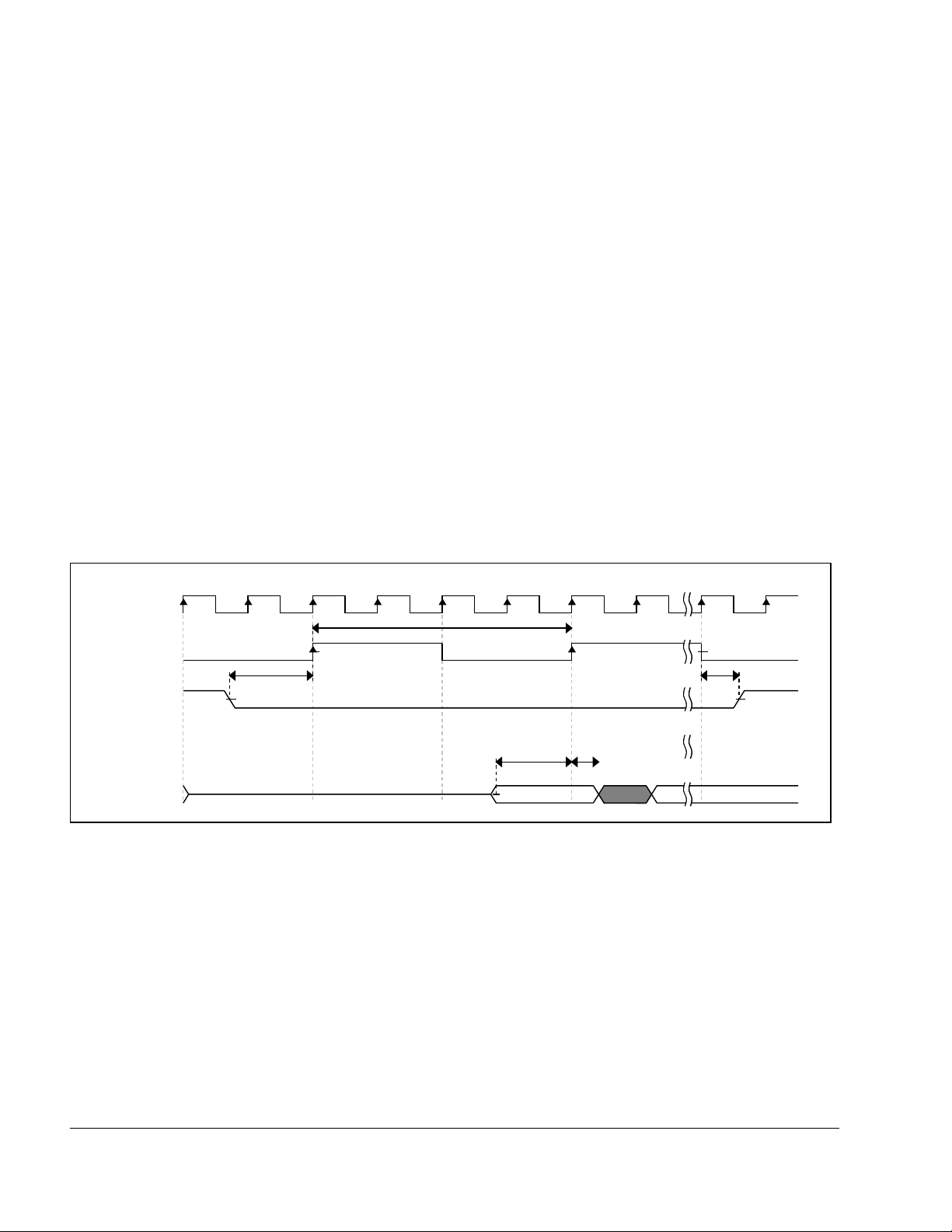
1 2 3
Tck
Tcss Tcsh
Tis
Tih
Clock
SFCK
CS
Data in
Specifications—real-time domain
9.1 Power sequencing—real-time domain
See Power sequencing—system.
9.2 Peripheral operating requirements and behaviors—real-time domain
9.2.1 QuadSPI AC specifications
• All data is based on a negative edge data launch from the device and a positive
edge data capture, as shown in the timing diagrams in this section.
• Measurements are with a load of 10 pF on output pins. Input slew: 2 ns
• Timings assume a setting of 0x0004_000x for QuadSPI _SMPR register (see the
reference manual for details).
SDR mode
Figure 27. QuadSPI input timing (SDR mode) diagram
NOTE
• The timing values below are with default settings for
sampling registers like QuadSPI_SMPR.
• A negative time indicates the actual capture edge inside
the device is earlier than clock appearing at pad.
• Frequency calculator guidelines (Max read frequency) for
any frequency: SCR > (Flash access time)max + (Tis)max
80
NXP Semiconductors
i.MX 7ULP Applications Processor—Consumer, Rev. 0, 09/2020
Page 81
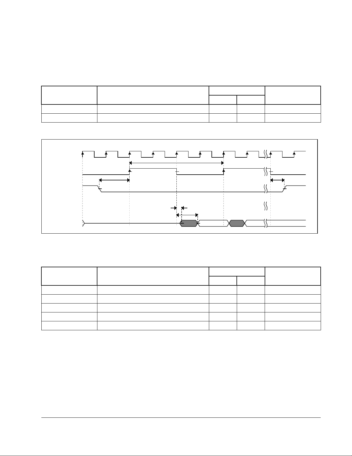
1 2 3
Toh
Tov
Tck
Tcss Tcsh
Clock
SFCK
CS
Data out
Specifications—real-time domain
• All board delays need to be added appropriately
• Input hold time being negative does not have any
implication or max achievable frequency
Table 45. QuadSPI input timing (SDR mode) specifications
Symbol Parameter Value Unit
Min Max
T
is
T
ih
Setup time for incoming data 6 — ns
Hold time requirement for incoming data 1 — ns
Symbol Parameter Value Unit
T
ov
T
oh
T
ck
T
css
T
csh
DDR Mode
Figure 28. QuadSPI output timing (SDR mode) diagram
Table 46. QuadSPI output timing (SDR mode) specifications
Min Max
Output Data Valid — 2 ns
Output Data Hold 3 — ns
SCK clock period — 99 MHz
Chip select output setup time 5 — ns
Chip select output hold time 5 — ns
NOTE
For any frequency, setup and hold specifications of the
memory should be met.
i.MX 7ULP Applications Processor—Consumer, Rev. 0, 09/2020
81
NXP Semiconductors
Page 82

1 2 3
Tck
Tcss Tcsh
Tis
Tih
Clock
SFCK
CS
Data in
1 2 3
Tck
Tcss Tcsh
Tov
Toh
Clock
SFCK
CS
Data out
Specifications—real-time domain
Figure 29. QuadSPI input timing (DDR mode) diagram
• Parameters assume a load of 10 pf
• The parameters are for setting of hold condition in
register QuadSPI_SMPR[DDRSMP]
• Read frequency calculations should be: SCK/2 > (flash
access time) + Setup (Tis) - (edge number) x SCK/4
NOTE
Table 47. QuadSPI input timing (DDR mode) specifications
Symbol Parameter Value Unit
Min Max
T
T
Setup time for incoming data 6 — ns
is
Hold time requirement for incoming data 1 — ns
ih
Figure 30. QuadSPI output timing (DDR mode) diagram
82
NXP Semiconductors
i.MX 7ULP Applications Processor—Consumer, Rev. 0, 09/2020
Page 83
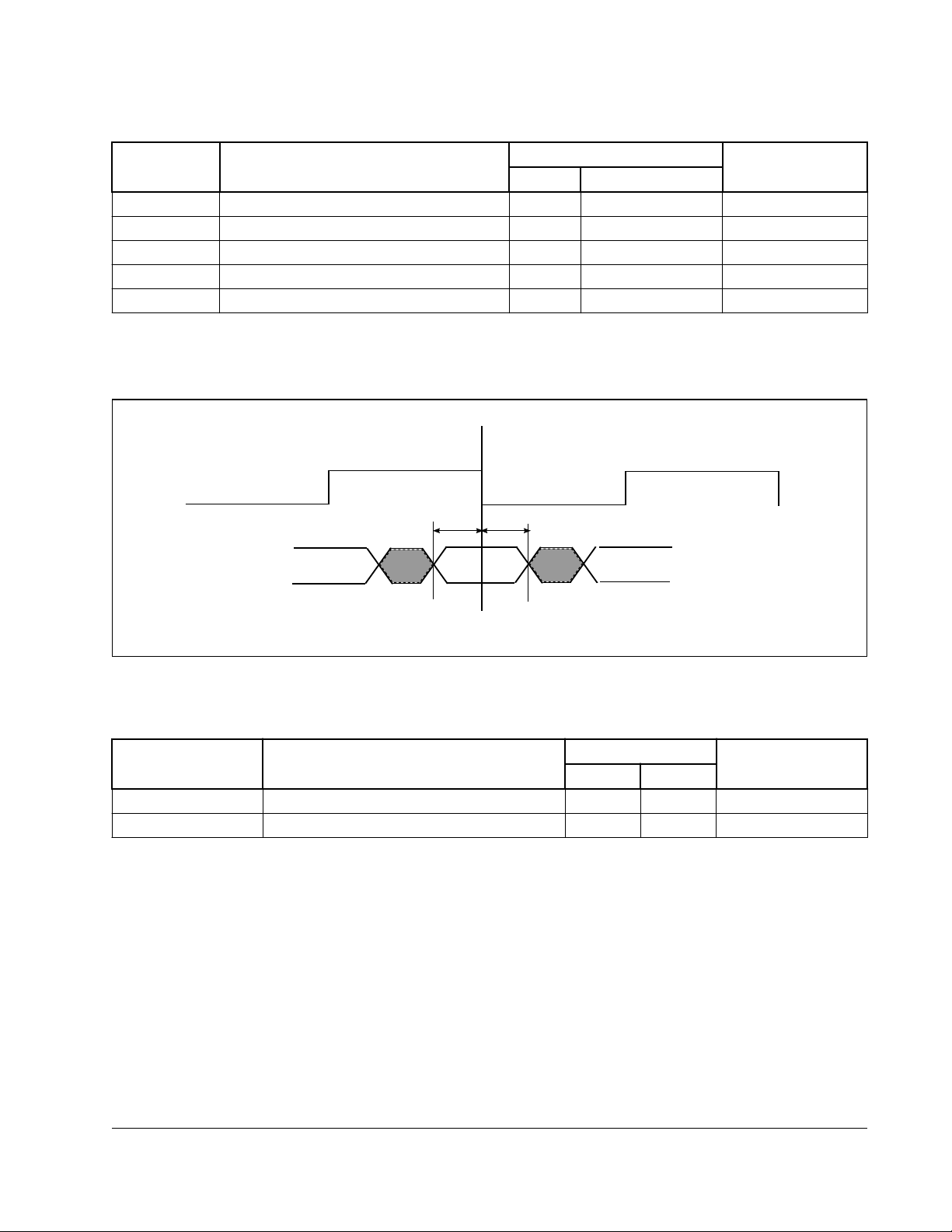
Ts
MIN
QSPI_SCLK
DI[7:0]
Th
MIN
Specifications—real-time domain
Table 48. QuadSPI output timing (DDR mode) specifications
Symbol Parameter Value Unit
Min Max
T
ov
T
oh
T
ck
T
css
T
csh
Output Data Valid - 1.75 ns
Output Data Hold 2 - ns
SCK clock period - 60 MHz
Chip select output setup time 2.7 - Clk(sck)
Chip select output hold time 5.62 - Clk(sck)
Hyperflash mode
Symbol Parameter Value Unit
Ts
MIN
Th
MIN
Figure 31. QuadSPI input timing (Hyperflash mode) diagram
Table 49. QuadSPI input timing (Hyperflash mode) specifications
Min Max
Setup time for incoming data 6 - ns
Hold time requirement for incoming data 1 - ns
i.MX 7ULP Applications Processor—Consumer, Rev. 0, 09/2020
83
NXP Semiconductors
Page 84
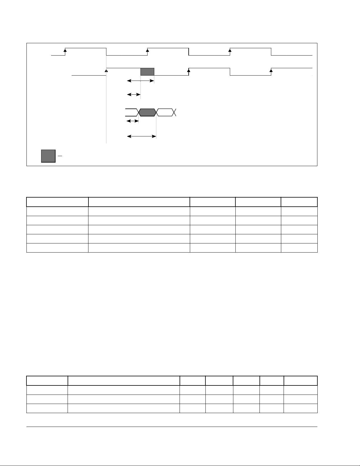
QSPI_SCLK
QSPI_SCLK_B
T
HO
T
DVO
Tclk
SKMAX
Tclk
SKMIN
Output Invalid Data
Specifications—real-time domain
Figure 32. QuadSPI output timing (Hyperflash mode) diagram
Table 50. QuadSPI output timing (Hyperflash mode) specifications
TdvMAX Output Data Valid ─ 4.3 ns
Tho Output Data Hold 1.3 ─ ns
TclkSKMAX Ck to DQS skew max ─ CK/2 + 0.8 ns
TclkSKMIN Ck to DQS skew min -(CK/2 + 1.2) ─ ns
Tck CK clock period ─ 70 MHz
9.2.2
9.2.2.1 12-bit ADC electrical specifications
All ADC channels meet the 12-bit single-ended accuracy specifications.
Table 51. ADC Electrical Specifications (VREFH=VDD_ANA_18 and VADIN
Symbol Description Min Typ Max Unit Notes
VADIN Input voltage VREFL VREFH V
CADIN Input capacitance 4.5 pF
RADIN Input resistance 500 Ω
Symbol Characteristic Min Max Unit
NOTE
Maximum QSPI clock frequency = 70 MHz.
Analog modules
≤VREFH)
max
84
NXP Semiconductors
Table continues on the next page...
i.MX 7ULP Applications Processor—Consumer, Rev. 0, 09/2020
Page 85

Specifications—real-time domain
Table 51. ADC Electrical Specifications (VREFH=VDD_ANA_18 and VADIN
max
(continued)
Symbol Description Min Typ Max Unit Notes
RAS Analog source resistance 5 KΩ 1
fADCK ADC Conversion clock frequency 8 66 MHz
Csample Sample cycles 3.5 131.5 2
Ccompare Fixed compare cycles 17.5 cycles
Cconversion Conversion cycles Cconversion= Csample +
Ccompare
TUE Total unadjusted Error -14 to -2 LSB 3
DNL Differential nonlinearity ±1.2 LSB 3,4
INL Integral nonlinearity ±1.2 LSB 3,4
ENOB Effective number of bits 5
Single-ended mode
Avg = 1 10.5
Avg = 2 10.8
Avg = 16 11.4
Differential mode
Avg = 1 11.4
Avg = 2 —
Avg = 16 —
SINAD Signal to noise plus distortion SINAD=6.02 x ENOB + 1.76 dB
EFS Full-scale error -4 LSB 3
EZS Zero-scale error 0.05 LSB 3
EIL Input leakage error RAS * Iin mV
cycles
≤VREFH)
1. This resistance is external to the SoC. To achieve the best results, the analog source resistance must be kept as low
as possible. The results in this data sheet were derived from a system that had < 15 Ω analog source resistance. The
RAS/CAS time constant should be kept to < 1 ns.
2. See Sample time vs. RAS.
3. 1 LSB = (VREFH - VREFL)/2N, N=12
4. ADC conversion clock at max frequency and using linear histogram.
5. Input data used for test was 1 kHz sine wave.
Table 52. ADC electrical specifications (VREFH=1.68 V and
VADIN
Symbol Description Min Typ2 Max Unit Notes
VADIN Input voltage—
Port A
Input voltage—
Port B
CADIN Input
capacitance
i.MX 7ULP Applications Processor—Consumer, Rev. 0, 09/2020
≤VDD_PTA
max
VREFL VDD_PTA
Table continues on the next page...
)1
max
4.5 pF
VDD_PTB
max
max
V
NXP Semiconductors
85
Page 86
Specifications—real-time domain
Table 52. ADC electrical specifications (VREFH=1.68 V and VADIN
max
(continued)
Symbol Description Min Typ2 Max Unit Notes
RADIN Input resistance 1 KΩ
RAS Analog source
resistance
fADCK ADC
conversion
clock frequency
Csample Sample cycles 3.5 131.5 4
Ccompare Fixed compare
cycles
Cconversion Conversion
cycles
TUE Total
unadjusted
error
DNL Differential
nonlinearity
INL Integral
nonlinearity
ENOB Effective Number of Bits 7
Single-ended mode
Avg = 1 10.3
Avg = 2 10.6
Avg = 16 11.3
Differential mode
Avg = 1 11.2
Avg = 2 —
Avg = 16 —
SINAD Signal to noise
plus distortion
EFS Full-scale error -4 LSB 5
EZS Zero-scale error 0.05 LSB 5
EIL Input leakage
error
8 66 MHz
17.5 Cycles
Cconversion= Csample + Ccompare Cycles
-14 to -2 LSB 5
±1.2 LSB 5,6
±1.2 LSB 5,6
SINAD=6.02 x ENOB + 1.76 dB
RAS * Iin mV
5 KΩ 3
≤VDD_PTA
max
)1
1. Values in this table are based on design simulations.
2. Typical values assume VDD_ANA_18 = 1.8 V, Temp = 25 °C, fACLK = Max, unless otherwise stated. Typical values are
for reference only, and are not tested in production.
3. This resistance is external to the SoC. To achieve the best results, the analog source resistance must be kept as low as
possible. The results in this data sheet were derived from a system that had < 15 Ω analog source resistance. The
RAS/CAS time constant should be kept to < 1 ns.
4. See Sample time vs. RAS.
5. 1 LSB = (VREFH - VREFL)/2N, N=12
6. ADC conversion clock at max frequency and using linear histogram.
7. Input data used for test was 1 kHz sine wave.
86
NXP Semiconductors
i.MX 7ULP Applications Processor—Consumer, Rev. 0, 09/2020
Page 87

Specifications—real-time domain
Table 53. ADC electrical specifications (1V≤VREFH<VDD_ANA18
VADIN
Symbol Description Min Typ2 Max Unit Notes
VADIN Input voltage VREFL VREFH V
CADIN Input
RADIN Input
RAS Analog
fADCK ADC
Csample Sample
Ccompare Fixed
Cconversion Conversion
TUE Total
DNL Differential
INL Integral
ENOB Effective number of bits 7
SINAD Signal to
EFS Full-scale
EZS Zero-scale
EIL Input leakage
≤VREFH)1
MAX
capacitance
resistance
source
resistance
8 44 MHz
conversion
clock
frequency
3.5 131.5 4
cycles
compare
cycles
Cconversion= Csample + Ccompare Cycles
cycles
unadjusted
error
nonlinearity
nonlinearity
Single-ended mode
Avg = 1 9.8
Avg = 2 10.2
Avg = 16 11.1
Differential mode
Avg = 1 10.7
Avg = 2 —
Avg = 16 —
SINAD=6.02 x ENOB + 1.76 dB
noise plus
distortion
error
error
RAS * Iin mV
error
4.5 pF
500 Ω
5 KΩ 3
17.5 Cycles
-14 to -2 LSB 5
±1.2 LSB 5,6
±1.2 LSB 5,6
-4 LSB 5
0.05 LSB 5
MIN
and
i.MX 7ULP Applications Processor—Consumer, Rev. 0, 09/2020
87
NXP Semiconductors
Page 88
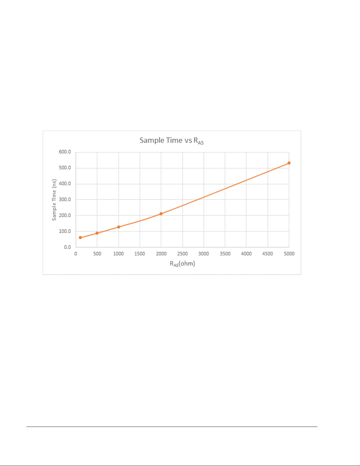
Specifications—real-time domain
1. Values in this table are based on design simulations.
2. Typical values assume VDD_ANA_18 = 1.8 V, Temp = 25 °C, fACLK = Max, unless otherwise stated. Typical values are
for reference only, and are not tested in production.
3. This resistance is external to the SoC. To achieve the best results, the analog source resistance must be kept as low as
possible. The results in this data sheet were derived from a system that had < 15 Ω analog source resistance. The
RAS/CAS time constant should be kept to < 1 ns.
4. See Sample time vs. RAS.
5. 1 LSB = (VREFH - VREFL)/2N, N=12
6. ADC conversion clock at max frequency and using linear histogram.
7. Input data used for test was 1 kHz sine wave.
The following figure shows a plot of the ADC sample time versus RAS.
88
NXP Semiconductors
Figure 33. Sample time vs. R
i.MX 7ULP Applications Processor—Consumer, Rev. 0, 09/2020
AS
Page 89
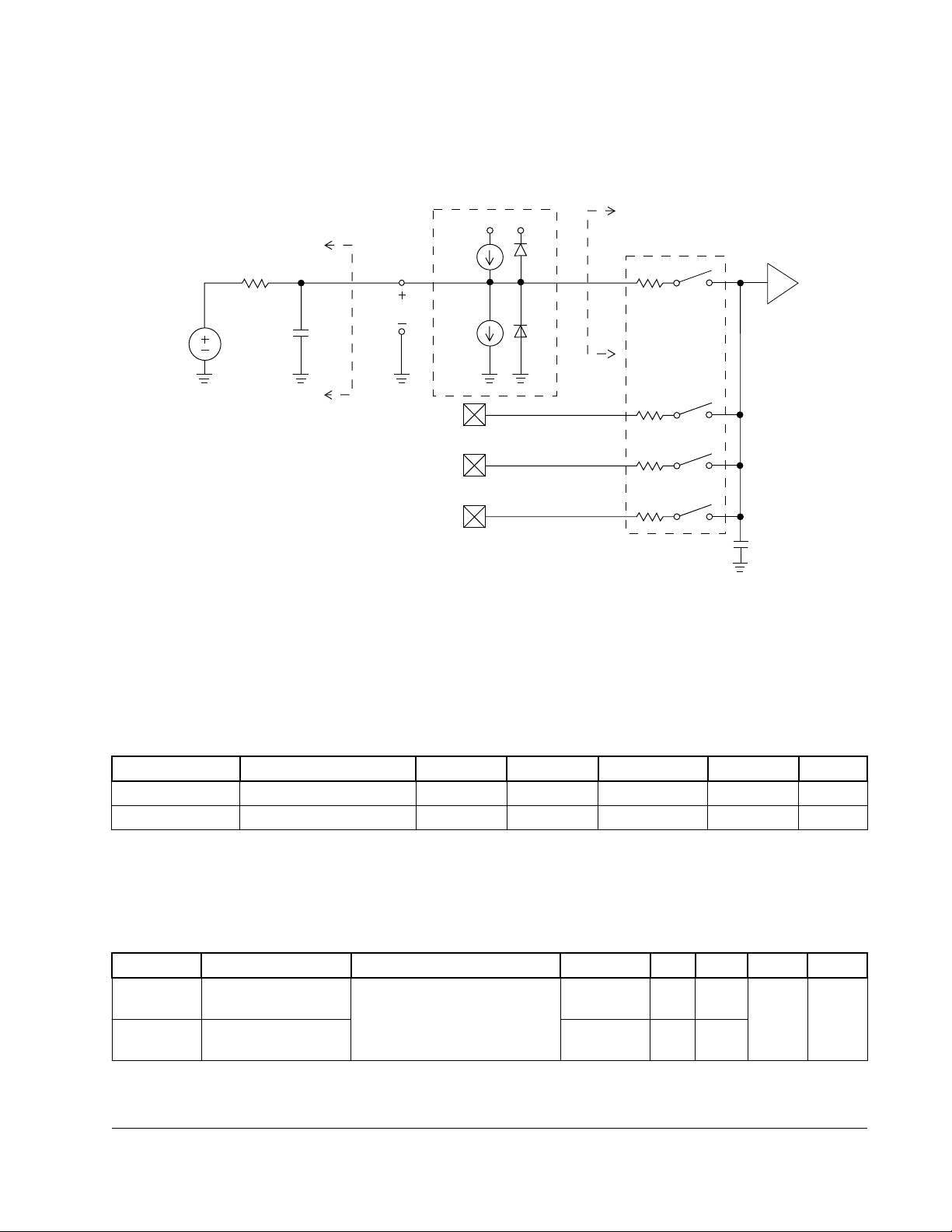
9.2.2.1.1 12-bit ADC operating conditions
RAS
VAS
CAS
ZAS
VADIN
ZADIN
RADIN
RADIN
RADIN
RADIN
CADIN
Pad
leakage
INPUT PIN
INPUT PIN
INPUT PIN
SIMPLIFIED
INPUT PIN EQUIVALENT
CIRCUIT
SIMPLIFIED
CHANNEL SELECT
CIRCUIT
ADC SAR
ENGINE
Specifications—real-time domain
Figure 34. ADC input impedance equivalency diagram
9.2.2.2
12-bit DAC electrical characteristics
9.2.2.2.1 12-bit DAC operating requirements
Table 54. 12-bit DAC operating conditions
Symbol Description Min Typ Max Unit Notes
C
L
I
L
1. The DAC output can drive R and C loading. The user should consider both DC and dynamic application requirements.
50pF CL provides the best dynamic performance, while 100pF provides the best DC performance.
2. Sink or source current ability.
Symbol Description Test Conditions Min Typ Max Units Notes
VDACOUTL DAC low level output
VDACOUTH DAC high level output
Output load capacitance — 50 100 pF 1
Output load current — — 1 mA 2
Table 55. DAC characteristics
voltage
voltage
VREFH_ANA18 selected,
Rload=18k, Cload=50pF
VSS — 0.15 V 1
VDD_ANA18
-0.15
— VDD_
ANA18
i.MX 7ULP Applications Processor—Consumer, Rev. 0, 09/2020
Table continues on the next page...
89
NXP Semiconductors
Page 90

Specifications—real-time domain
Table 55. DAC characteristics (continued)
Symbol Description Test Conditions Min Typ Max Units Notes
DNL Differential non-
linearity error
INL Integral non-linearity
error
EO Offset error Code 100h — ±0.6 — %FSR —
TEO Offset error
temperature coefficient
EG Gain error Code F00h — ±0.4 — %FSR —
TEG Gain error temperature
coefficient
TFS_LS Full scale setting time
in Low Speed mode
TFS_MS Full scale setting time
in Middle Speed mode
TFS_HS Full scale setting time
in High Speed mode
TCC_LS Code to code setting
time in Low Speed
mode
TCC_MS Code to code setting
time in Middle Speed
mode
TCC_HS Code to code setting
time in High Speed
mode
SR_LS Slew rate in Low
Speed mode
SR_MS Slew rate in Middle
Speed mode
SR_HS Slew rate in High
Speed mode
Code 100h → F00h best fit
curve
Code 100h → F00h best fit
curve
Code 100h — ±30 — µV/°C —
Code F00h — 10 — ppm of
Code → F00h or F00h → 100h
@ ZTC current
Code 100h → F00h or F00h →
100h @ PTAT current
Code 100h → F00h or F00h →
100h @ ZTC current
Code 100h → F00h or F00h →
100h @ PTAT current
Code 100h → F00h or F00h →
100h @ ZTC current
Code 100h → F00h or F00h →
100h @ PTAT current
Code 7F7h → 807h or 807h →
7F7h @ ZTC current
Code 7F7h → 807h or 807h →
7F7h @ PTAT current
Code 7F7h → 807h or 807h →
7F7h @ ZTC current
Code 7F7h → 807h or 807h →
7F7h @ PTAT current
Code 7F7h → 807h or 807h →
7F7h @ ZTC current
Code 7F7h → 807h or 807h →
7F7h @ PTAT current
Code 100h → F00h or F00h →
100h @ ZTC current
Code 100h → F00h or F00h →
100h @ PTAT current
Code 100h → F00h or F00h →
100h @ ZTC current
Code 100h → F00h or F00h →
100h @ PTAT current
Code 100h → F00h or F00h →
100h @ ZTC current
— ±0.5 ±1 LSB —
— ±1 — 2
— ±2 — 3
FSR/°C
— 5 — µs 4
— 5 —
— 1 —
— 1 —
— 0.5 —
— 0.5 —
— 1 —
— 1 —
— 0.5 —
— 0.5 —
— 0.3 —
— 0.3 —
— 0.24 — V/µs 5
— 0.24 —
— 1.2 —
— 1.2 —
— 2.4 —
—
90
NXP Semiconductors
Table continues on the next page...
i.MX 7ULP Applications Processor—Consumer, Rev. 0, 09/2020
Page 91
Specifications—real-time domain
Table 55. DAC characteristics (continued)
Symbol Description Test Conditions Min Typ Max Units Notes
Code 100h →F00h or F00h →
100h @ PTAT current
PSRR Power supply rejection
ratio
Glitch Glitch energy Code 100h → F00h → 100h — 30 — nV-s —
CT Channel to channel
crosstalk
ROP Output resistance Code 100h → F00h and
1. It is recommended to operate the DAC in the output voltage range between 0.15 V and (VDD_ANA18 - 0.15 V) for
best accuracy. Linearity of the output voltage outside this range will be affected as current load increases.
2. When VREFH_ANA18 is selected as the reference (DAC_CR[DACRFS]=1b).
3. When the internal 1.2 V source is selected as the reference (DAC_CR[DACRFS]=1b).
4. The DAC output remains within ±0.5 LSB of the final measured value for digital input code change. Noise on the
power supply can cause this performance to degrade to ±1 LSB. This parameter represents both rising edge and
falling edge settling time.
5. Time for the DAC output to transition from 10% to 90% signal amplitude (rising edge or falling edge).
6. PSRR=20*log{∆VDD_ANA18 /∆VDAC_OUT}
7. If two DACs are used and sharing the same VREFH.
8. Based on design simulation.
Code 800h,
ΔVDD_ANA18=100mV,
VREFH_ANA12 selected
Code 7FFh → 800h → 7FFh — 30 —
— — — -80 dB 7
Rload=18kΩ
— 2.4 —
— 70 — dB 6
— 200 — Ω 8
9.2.2.3 CMP electrical specifications
Table 56. CMP Operating Conditions
Symbol Description Min Typ Max Unit
VREFH_EXT External reference voltage 1 — 1.98 V
VREFH_INT
1. This is an internally generated voltage reference generated by PMC0.
Symbol Description Condition Min Typ Max Unit
VAIN Analog input voltage 0 VDD_PTx
VAIO Analog input offset
VH Analog comparator
1
voltage
hysteresis
Internal reference voltage — 1.3 — V
Table 57. CMP Characteristics
, 1
20 mV
Hysctrl[1:0]=00 5 mV
Hysctrl[1:0]=01 10 mV
Hysctrl[1:0]=10 20 mV
Hysctrl[1:0]=11 30 mV
Table continues on the next page...
V
i.MX 7ULP Applications Processor—Consumer, Rev. 0, 09/2020
91
NXP Semiconductors
Page 92

Specifications—real-time domain
Table 57. CMP Characteristics (continued)
Symbol Description Condition Min Typ Max Unit
TDHS Propagation delay,
high-speed mode
TDHS Propagation delay,
low-speed mode
Analog comparator
initialization delay
INL 8B DAC integral non-
linearity
DNL 8B DAC differential
non-linearity
1. The maximum input voltage for CMP analog inputs associated with Port A (PTA) is VDD_PTA. The maximum input
voltage for CMP analog inputs associated with Port B (PTB) is VDD_PTB.
Nominal supply 50 ns
5 µs
20 µs
-1 1 LSB
-1 1 LSB
9.2.3 Timer specifications—real-time domain
See General switching timing specifications.
9.2.4
Connectivity and communications specifications—real-time domain
9.2.4.1 LPUART
See General switching timing specifications.
9.2.4.2
See Inter-Integrated Circuit Interface (I2C) timing.
9.2.4.3
See Low Power Serial Peripheral Interface (LPSPI) switching specifications—
application domain.
Inter-Integrated Circuit Interface (I2C) timing—real-time domain
LPSPI switching specifications—real-time domain
9.2.4.4
I2S/SAI switching specifications
This section provides the AC timing for the I2S/SAI module in master mode (clocks are
driven) and slave mode (clocks are input). All timing is given for noninverted serial
clock polarity (TCR2[BCP] is 0, RCR2[BCP] is 0) and a noninverted frame sync
92
NXP Semiconductors
i.MX 7ULP Applications Processor—Consumer, Rev. 0, 09/2020
Page 93

S1 S2 S2
S3
S4
S4
S5
S9
S7
S9 S10
S7
S8
S6
S10
S8
I2S_MCLK (output)
I2S_TX_BCLK/
I2S_RX_BCLK (output)
I2S_TX_FS/
I2S_RX_FS (output)
I2S_TX_FS/
I2S_RX_FS (input)
I2S_TXD
I2S_RXD
Specifications—real-time domain
(TCR4[FSP] is 0, RCR4[FSP] is 0). If the polarity of the clock and/or the frame sync
have been inverted, all the timing remains valid by inverting the bit clock signal
(BCLK) and/or the frame sync (FS) signal shown in the following figures.
Table 58. I2S/SAI master mode timing
Num. Parameter Min Max Unit
S1 I2S_MCLK cycle time 20 — ns
S2 I2S_MCLK (as an input) pulse width high/low 45% 55% MCLK period
S3 I2S_TX_BCLK/I2S_RX_BCLK cycle time (output) 40 — ns
S4 I2S_TX_BCLK/I2S_RX_BCLK pulse width high/low 45% 55% BCLK period
S5 I2S_TX_BCLK/I2S_RX_BCLK to I2S_TX_FS/I2S_RX_FS
output valid
S6 I2S_TX_BCLK/I2S_RX_BCLK to I2S_TX_FS/I2S_RX_FS
output invalid
S7 I2S_TX_BCLK to I2S_TXD valid — 15.9 ns
S8 I2S_TX_BCLK to I2S_TXD invalid 1 — ns
S9 I2S_RXD/I2S_RX_FS input setup before I2S_RX_BCLK 21.3 — ns
S10 I2S_RXD/I2S_RX_FS input hold after I2S_RX_BCLK 0 — ns
— 7.5 ns
0 — ns
Figure 35. I2S/SAI timing — master modes
Table 59. I2S/SAI slave mode timing
Num. Parameter Min Max Unit
S11 I2S_TX_BCLK/I2S_RX_BCLK cycle time (input) 40 — ns
S12 I2S_TX_BCLK/I2S_RX_BCLK pulse width high/low (input) 45% 55% MCLK period
i.MX 7ULP Applications Processor—Consumer, Rev. 0, 09/2020
Table continues on the next page...
NXP Semiconductors
93
Page 94

S15
S13
S15
S17 S18
S15
S16
S16
S14
S16
S11
S12
S12
I2S_TX_BCLK/
I2S_RX_BCLK (input)
I2S_TX_FS/
I2S_RX_FS (output)
I2S_TXD
I2S_RXD
I2S_TX_FS/
I2S_RX_FS (input)
S19
Specifications—real-time domain
Table 59. I2S/SAI slave mode timing (continued)
Num. Parameter Min Max Unit
S13 I2S_TX_FS/I2S_RX_FS input setup before I2S_TX_BCLK/
I2S_RX_BCLK
S14 I2S_TX_FS/I2S_RX_FS input hold after I2S_TX_BCLK/
I2S_RX_BCLK
S15 I2S_TX_BCLK to I2S_TXD/I2S_TX_FS output valid — 22.8 ns
S16 I2S_TX_BCLK to I2S_TXD/I2S_TX_FS output invalid 1 — ns
S17 I2S_RXD setup before I2S_RX_BCLK 12 — ns
S18 I2S_RXD hold after I2S_RX_BCLK 1 — ns
S19 I2S_TX_FS input assertion to I2S_TXD output valid
1
1. Applies to first bit in each frame and only if the TCR4[FSE] bit is clear
13 — ns
1 — ns
— 17.0 ns
9.2.4.5
This section provides the operating performance for the device in VLPR, VLPW, and
VLPS modes.
Num. Parameter Min Max Unit
S1 I2S_MCLK cycle time 60 — ns
S2 I2S_MCLK pulse width high/low 45% 55% MCLK period
S3 I2S_TX_BCLK/I2S_RX_BCLK cycle time (output) 100 — ns
S4 I2S_TX_BCLK/I2S_RX_BCLK pulse width high/low 45% 55% BCLK period
S5 I2S_TX_BCLK/I2S_RX_BCLK to I2S_TX_FS/I2S_RX_FS
94
NXP Semiconductors
Figure 36. I2S/SAI timing — slave modes
VLPR, VLPW, and VLPS mode performance
Table 60. I2S/SAI master mode timing in VLPR, VLPW, and VLPS modes
output valid
Table continues on the next page...
i.MX 7ULP Applications Processor—Consumer, Rev. 0, 09/2020
— 15 ns
Page 95

S1 S2 S2
S3
S4
S4
S5
S9
S7
S9 S10
S7
S8
S6
S10
S8
I2S_MCLK (output)
I2S_TX_BCLK/
I2S_RX_BCLK (output)
I2S_TX_FS/
I2S_RX_FS (output)
I2S_TX_FS/
I2S_RX_FS (input)
I2S_TXD
I2S_RXD
Specifications—real-time domain
Table 60. I2S/SAI master mode timing in VLPR, VLPW, and VLPS modes (continued)
Num. Parameter Min Max Unit
S6 I2S_TX_BCLK/I2S_RX_BCLK to I2S_TX_FS/I2S_RX_FS
output invalid
S7 I2S_TX_BCLK to I2S_TXD valid — 25 ns
S8 I2S_TX_BCLK to I2S_TXD invalid 0 — ns
S9 I2S_RXD/I2S_RX_FS input setup before I2S_RX_BCLK 25 — ns
S10 I2S_RXD/I2S_RX_FS input hold after I2S_RX_BCLK 0 — ns
0 — ns
Figure 37. I2S/SAI timing — master modes
Table 61. I2S/SAI slave mode timing in VLPR, VLPW, and VLPS modes
Num. Parameter Min Max Unit
S11 I2S_TX_BCLK/I2S_RX_BCLK cycle time (input) 100 — ns
S12 I2S_TX_BCLK/I2S_RX_BCLK pulse width high/low (input) 45% 55% MCLK period
S13 I2S_TX_FS/I2S_RX_FS input setup before I2S_TX_BCLK/
I2S_RX_BCLK
S14 I2S_TX_FS/I2S_RX_FS input hold after I2S_TX_BCLK/
I2S_RX_BCLK
S15 I2S_TX_BCLK to I2S_TXD/I2S_TX_FS output valid — 40 ns
S16 I2S_TX_BCLK to I2S_TXD/I2S_TX_FS output invalid 1 — ns
S17 I2S_RXD setup before I2S_RX_BCLK 30 — ns
S18 I2S_RXD hold after I2S_RX_BCLK 5 — ns
S19 I2S_TX_FS input assertion to I2S_TXD output valid
1. Applies to first bit in each frame and only if the TCR4[FSE] bit is clear
1
i.MX 7ULP Applications Processor—Consumer, Rev. 0, 09/2020
30 — ns
2 — ns
— 27 ns
NXP Semiconductors
95
Page 96

S15
S13
S15
S17 S18
S15
S16
S16
S14
S16
S11
S12
S12
I2S_TX_BCLK/
I2S_RX_BCLK (input)
I2S_TX_FS/
I2S_RX_FS (output)
I2S_TXD
I2S_RXD
I2S_TX_FS/
I2S_RX_FS (input)
S19
Package information and contact assignments
Figure 38. I2S/SAI timing — slave modes
9.2.4.6 FlexIO specifications—real-time domain
See General switching timing specifications
10
This section contains package information and contact assignments for the following
packages:
• BGA 14 x 14 mm, 0.5 mm pitch (VP suffix)
• BGA 10 x 10 mm, 0.5 mm pitch (VK suffix)
10.1
This section includes the following information for the 14 x 14 mm, 0.5 mm pitch
package:
• Case outline
• Ball map
• Contact assignments
10.1.1
The following figure shows the top, bottom, and side views of the 14 × 14 mm BGA
package.
96
NXP Semiconductors
Package information and contact assignments
BGA, 14 x 14 mm, 0.5 mm pitch (VP suffix)
14 x 14 mm package case outline
i.MX 7ULP Applications Processor—Consumer, Rev. 0, 09/2020
Page 97

Package information and contact assignments
Figure 39. 14 x 14 mm case outline
i.MX 7ULP Applications Processor—Consumer, Rev. 0, 09/2020
97
NXP Semiconductors
Page 98
Package information and contact assignments
Figure 40. Notes on 14 x 14 mm case outline
10.1.2 14 x 14 mm, 0.5 mm pitch, ball map
The following page shows the 14 × 14 mm, 0.5 mm pitch, ball map.
98
NXP Semiconductors
i.MX 7ULP Applications Processor—Consumer, Rev. 0, 09/2020
Page 99
1 2 3 4 5 6 7 8 9 10 11 12 13 14 15 16 17 18 19 20 21 22 23 24 25 26 27
A
VSS PTF6 VDD18 _HSIC PTE15 PTE11 PTE5 PTE1 PTC12 PTC8 PTD11 PTD7 PTD4 PTD0 DDR_DQ16 VSS A
B
PTF5 PTF1 PTF2 VSS PTE14 PTE13 PTE12 PTE4 PTE3 PTE2 PTC11 PTC10 PTC9 PTD10 PTD9 PTD8 PTD3 PTD2 PTD1 DDR_DQ18 DDR_DQ17 B
C
PTF3 VSS VSS VSS VSS VSS VSS VSS VSS VSS VSS VSS VSS DDR_DQ19 C
D
PTF9 PTF0 VSS HSIC_DATA HSIC_STROBE VDD_HSIC PTE10 PTE6 VDD_PTE PTE0 PTC13 VDD_PTC PTC6 PTC5 PTC0 VDD_PTD PTD5 PTD6 DDR_DQ22 VSS DDR_DQ20 DDR_DQ21 D
E
PTF4 PTE7 VDD_PTE PTC19 PTC14 VDD_PTC PTC1 VDD_PTD VSS DDR_DQ23 E
F
PTF8 PTF7 VSS VDD_PTF VSS PTE8 PTC18 PTC15 PTC4 PTC2 VSS VSS VDD18_DDR VSS DDR_DQS2_B DDR_DQS2 F
G
VDD_PTF PTF10 PTF11 PTE9 PTC17 PTC16 PTC7 PTC3 VSS DDR_DQM2 G
H
PTF16 PTF17 VSS PTF15 PTF14 PTF13 PTF12 VSS VSS VDD_DDR DDR_VREF0 DDR_DQ2 VSS DDR_DQ0 DDR_DQ1 H
J
PTF18 VDD_DDR DDR_CA4 DDR_CA3 DDR_DQ3 J
K
RESET1_B PTF19 VSS VSS VSS VDD_DIG1 VDD_DIG1 VDD_DIG1 VSS VDD_DIG1 VDD_DIG1 VDD_DIG1 VSS DDR_DQ4 VSS DDR_DQ6 DDR_DQ5 K
L
DSI_DATA1_N VSS VDD_DSI11 VDD18_IOREF VDD_DIG1 VSS VSS VSS VDD_DIG1 VSS VSS VSS VDD_DIG1 DDR_DQ7 L
M
DSI_CLK_P DSI_CLK_N VSS DSI_DATA1_P VDD_DSI18 VSS VSS VDD_DIG1 VSS VSS VSS VDD_DIG1 VSS VDD_DDR DDR_CA2 DDR_DQM0 VSS DDR_DQS0 DDR_DQS0_B M
N
VSS VDD_DIG1 VSS VSS VSS VDD_DIG1 VDD_DDR DDR_CA1 DDR_CA0 DDR_CS1_B N
P
DSI_DATA0_P DSI_DATA0_N VSS VSS VSS VDD_DIG1 VSS VSS VSS VSS VSS VDD_DIG1 VSS DDR_CKE1 VSS DDR_CKE0 DDR_CS0_B P
R
VSS VDD_USB33 VSS VDD_USB18 VDD_DI G1 VSS VSS VSS VDD_DIG1 DDR_CLK0 R
T
USB0_DP USB0_DM VSS
USB0_VBUS_DETEC
T
VDD_VBAT42 VDD_VBAT18_CAP VSS
VDD_PMC11_DIG1
_CAP
VSS VSS VSS VDD_DIG1 VDD_DDR DDR_CA6 DDR_CA5 DDR_DQS1_B VSS DDR_CLK0_B DDR_DQM1 T
U
VSS
VDD_PMC11_DIG1
_CAP
VSS VSS VSS
VDD_PMC11_DIG0
_CAP
VSS VSS VSS VDD_DIG1 VSS VDD_DDR DDR_CA7 DDR_DQS1 U
V
PMIC_ON_REQ STANDBY_REQ VSS_ANA TAMPER VSS VDD_PMC18_DIG0 VDD_PMC18_DIG0 VDD_PMC18_DIG0 VSS
VDD_PMC11_DIG0
_CAP
VDD_DIG0 VDD_DIG0 VSS DDR_DQ8 VSS DDR_DQ10 DDR_DQ9 V
W
EXTAL32 VSS VSS VDD_PLL18 DDR_DQ11 W
Y
VSS ONOFF VSS XTAL32 VSS VSS VSS VSS VDD_DDR DDR_CA9 DDR_VREF1 DDR_DQ15 DDR_DQ14 DDR_DQ12 DDR_DQ13 Y
AA
XTAL0 TESTCLK_N VDD_PTB VDD_ANA33 VDD_PTA VSS VDD_PTA DDR_ODT DDR_CA8 DDR_DQM3 AA
AB
VSS EXTAL0 VDD_PMC18 VDD_PMC12_DIG1 PTB11 TESTCLK_P VDD_ANA18 VREFL_ANA PTA6 PTA8 PTA19 PTA21 VSS VSS DDR_DQS3 DDR_DQS3_B AB
AC
VDD_PMC12_DIG1 PTB10 PTB12 RESET0_b VREFH_ANA18 PTA5 PTA9 PTA18 PTA22 DDR_DQ24 AC
AD
VSS VSS VSS VSS VDD_PTB PTB9 PTB13 PTB19 DAC0_OUT VSS_ADC_ANA PTA7 PTA4 PTA10 PTA11 PTA17 PTA23 PTA20 PTA29 PTA30 VSS DDR_DQ27 DDR_DQ26 AD
AE
VSS PTB2 PTB3 VSS VSS VSS DAC1_OUT PTA0 VSS VSS VSS VSS VSS DDR_DQ30 AE
AF
VSS PTB1 PTB5 PTB6 PTB7 PTB15 PTB16 PTB17 VSS_ADC_ANA PTA1 PTA3 PTA13 PTA14 PTA15 PTA24 PTA26 PTA27 PTA31 DDR_DQ31 DDR_DQ25 DDR_DQ28 AF
AG
VSS PTB0 PTB4 PTB8 PTB14 PTB18 VSS_ADC_ANA PTA2 PTA12 PTA16 PTA25 PTA28 DDR_ZQ0 DDR_DQ29 VSS AG
1 2 3 4 5 6 7 8 9 10 11 12 13 14 15 16 17 18 19 20 21 22 23 24 25 26 27
Package information and contact assignments
14 x 14 mm, 0.5 mm pitch, ballmap
i.MX 7ULP Applications Processor—Consumer, Rev. 0, 09/2020
99
NXP Semiconductors
Page 100

Package information and contact assignments
10.1.3 14 x 14 mm power supply and functional contact assignments
The following table shows the power supply contact assignments for the 14 × 14 mm
package.
Table 62. 14 x 14 mm power supply contact assignments
Supply Name 14x14 mm VP Package Ball
Position
DDR_ODT AA22 DDR on-die termination
DDR_VREF0 H23 DDR voltage reference input. Connect to a voltage
source that is 50% of VDD_DDR.
DDR_VREF1 Y23 DDR voltage reference input. Connect to a voltage
source that is 50% of VDD_DDR.
DDR_ZQ0 AG24 Connect DDR_ZQ0 to an external 240Ω 1% resistor to
Vss. This is a reference used during DDR output
buffer driver calibration.
TESTCLK_N AA8 Test function for NXP use only. This output must
remain unconnected.
TESTCLK_P AB8 Test function for NXP use only. This output must
remain unconnected.
USB0_VBUS T4 USB0 VBUS detection
VDD_ANA18 AB11 ADC analog and IO 1.8V supply input
VDD_ANA33 AA12 ADC analog and IO 3.3V supply input
VDD_DDR H22, J21, M22, N21, T21, U22, Y21 DDR I/O supply input
VDD_DIG0 V16, V17 M4 domain core and logic supply input
VDD_DIG1 K11, K12, K13, K15, K16, K17, L10,
L14, L18, M10, M18, N10, N18, P11,
P17, R10, R18, T18, U18
VDD_DSI11 L6 MIPI DSI 1.1V supply input
VDD_DSI18 M5 MIPI DSI 1.8V supply input
VDD_HSIC D6 HSIC 1.2V supply input
VDD_PLL18 W7 PLL analog supply input
VDD_PMC11_DIG0_CAP U14, V15 M4 domain LDO supply output
VDD_PMC11_DIG1_CAP T10, U10 A7 domain LDO supply output
VDD_PMC12_DIG1 AB4, AC4 A7 domain LDO and internal memory LDO supply
VDD_PMC18 AB3 M4/A7 PMC and PMC IO supply input
VDD_PMC18_DIG0 V11, V12, V13 M4 domain LDO and internal memory LDO supply
VDD_PTA AA15, AA19 GPIO Port A supply input
VDD_PTB AA11, AD6 GPIO Port B supply input
A7 domain core and logic supply input
input
input
Remarks
100
NXP Semiconductors
Table continues on the next page...
i.MX 7ULP Applications Processor—Consumer, Rev. 0, 09/2020
 Loading...