

Page 1

GPIO Expander
Cost-effective, flexible options from
the I2C-bus leader
NXP_03_0159_GPIO_Expander_Trifold_939775016987_v2_8,5x11.indd 3 10/09/10 12:34
Page 2
NXP’s general-purpose input/output (GPIO) expanders are a simple, cost-effective way to monitor and control several peripheral
5.0V
signals. They make it easy for designers to add extra I/O to their design and thereby free up the microprocessor’s GPIO for other,
more important functions. NXP is the industry leader in serial-interface GPIO expanders, and offers a broad selection of costeffective, easy-to-use options.
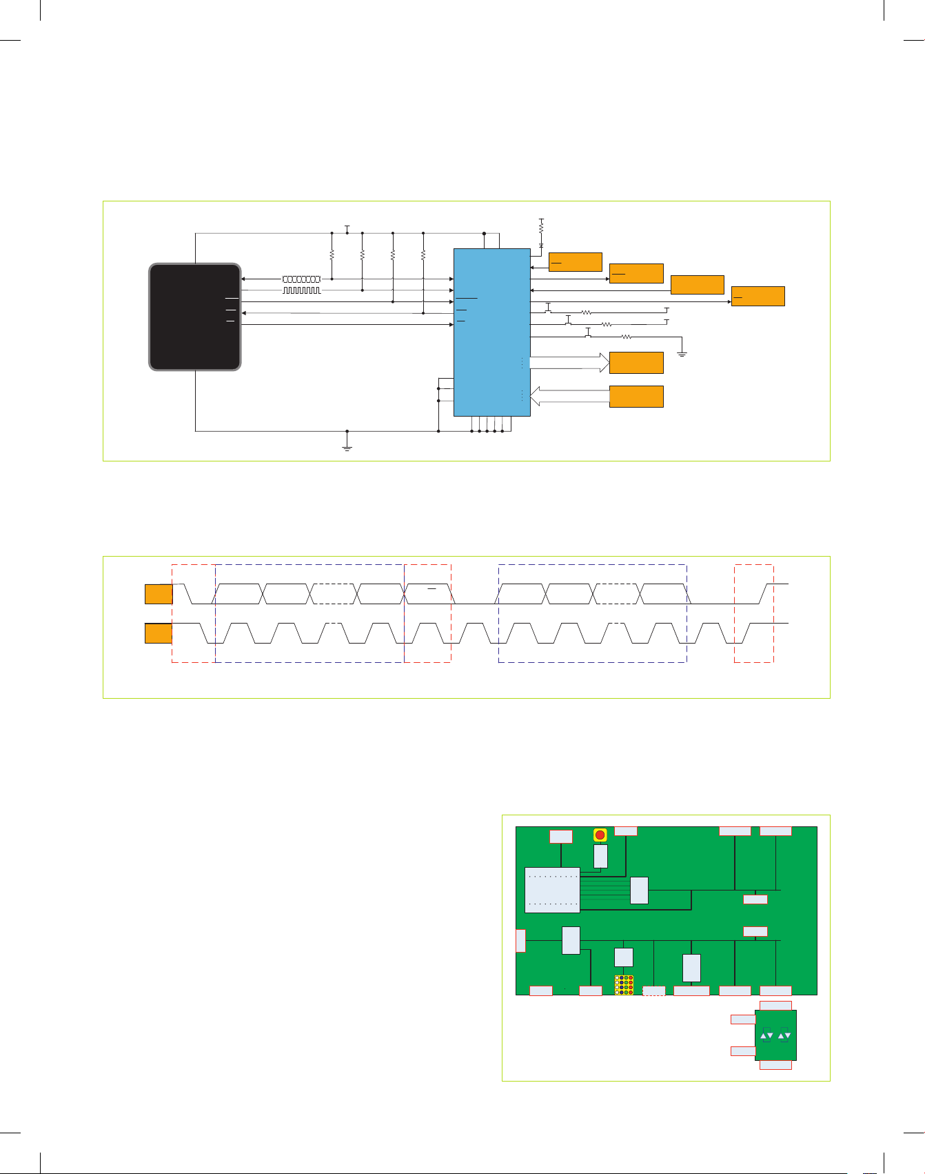
I2C-Bus GPIO Expander Application Example
VDD
MASTER
CONTROLLER
GND
SDA
SCL
RST
INT
OE
VDD = 2.3V to 5.5V
10KΩ Ω Ω Ω
10K 10K
10K
SDA
SCL
RESET
INT
OE
AD2
AD1
AD0
VDD
PCA9698
GND
IO0_0
IO0_1
IO0_2
IO0_3
IO0_4
IO0_5
IO0_6
IO0_7
IO1_0
IO1_7
IO2_0
IO2_7
2KΩ
SUBSYSTEM 1
Temp. Sens or
INT
Switch
Switch
10KΩ
Switch
SUBSYSTEM 2
Coun ter
RST
10KΩ
10KΩ
24 L ED Matrix
Alp hanu mer ic
Keyp ad
SUBSYSTEM 3
Alar m Syst em
ALARM
5.0V
5.0V
SUBSYSTEM 4
Memor y
CS
I2C-bus address = 0100 000x
The I2C-bus allows easy two-line communication between two devices using a serial data line (SDA) and a serial clock line (SCL)
and, as a result, is a popular choice for computing, consumer electronics, communication, and industrial systems.
I2C-Bus Communication Protocol and Timing Diagram
SDA
MSB
LSB
R/W
RX-ACK
MSB
LSB
RX-ACK
SCL
Start
Condition
1
2
Address Transfer
From Master to Slave
3-6 7
8
Data
Direction Bit
9
1 2
Data Transfer From Master to Slave (Write)
or Slave to Master (Read)
3-7 8
9
Stop
Condition
NXP’s I2C-bus GPIO expanders support three operating modes for data transfer: Standard Mode, with data transfer rates from
0 kbps to 100 kbps, Fast Mode (Fm), with data transfer rates from 0 kbps to 400 kbps, and Fast-mode Plus (Fm+) with data rates
from 0 kbps to 1 Mbps. Since the newer Fm+ GPIO are backward compatible all the way back to Standard Mode, it’s easy to
expand existing designs without changing the bus master device.
Application Support
NXP supports its GPIO expanders with several evaluation modules
UART
LED
PCA9901
8-pin SPI
connector
SPI
9-pin I2C-2005
connector
9-pin I2C-2005
connector
and demo boards that can be used to develop software and
evaluate performance.
The I2C-bus Fm+ Development Kit and associated GPIO daughter
cards provide a quick way to learn about the devices and the
I2C-bus protocol. The cards are modular, so they increase design
flexibility while providing easy access to the expander’s I/O pins.
For more information, visit ics.nxp.com/support/tools/interface
connector
USB
power jack
LPCXpresso
socket
LPC1343
SPI
5 V
8-pin SPI
connector
LED Bank
PCA9955
PCA9665
Fm+
I
2
C-bus
16-pin
connector
10-pin connector
to target board
Fm+
I
2
C-bus
Fm+
I
2
C-bus
PCA9672
GPIO
9-pin I2C-2005
connector
5-pin bus-buffer
connector
5-pin bus-buffer
connector
5-pin bus-buffer
connector
9-pin I2C-2005
connector
9-pin I2C-2005
connector
5-pin bus-buffer
002aaf760
connector
9-pin I2C-2005
connector
NXP_03_0159_GPIO_Expander_Trifold_939775016987_v2_8,5x11.indd 4 10/09/10 12:34
Page 3

GPIO Expander Selection Guide
[1]
[2]
Device
PCA8574 (A)
[3]
Function
Output Type
Number of I/O's
Operating Voltage Range
Standby Current
Max Output Drive Current
Max I/O Voltage Tolerance
Default POR Output State
Number of PWMs
Output Enable / PWM Control
GPIO Expander Quasi-Output 8 2.3 V - 5.5 V 4.5 µA 25 mA 5.5 V Hi-Z Input 0 N I2C, Fm 8 N Y Weak PU N In production
PCF8574 (A) GPIO Expander Quasi-Output 8 2.3 V - 6.0 V 2.5 µA 25 mA 5.5 V Hi-Z Input 0 N I
PCA9500 GPIO Expander Quasi-Output 8 2.5 V - 3.6 V 60 µA 25 mA 5.5 V High 0 N I
PCA9501 GPIO Expander Quasi-Output 8 2.5 V - 3.6 V 60 µA 25 mA 5.5 V High 0 N I
[4]
PCA9558
GPIO Expander Quasi-Output 8 3.0 V - 3.6 V 10 mA 4 mA 5.5 V Hi-Z Input 0 N I2C, Fm 2 N N Weak PU 2 Kbit In production
PCA9670 GPIO Expander Quasi-Output 8 2.3 V - 5.5 V 2.5 µA 25 mA 5.5 V Hi-Z Input 0 N I
PCA9672 GPIO Expander Quasi-Output 8 2.3 V - 5.5 V 2.5 µA 25 mA 5.5 V Hi-Z Input 0 N I
[3]
PCA9674 (A)
GPIO Expander Quasi-Output 8 2.3 V - 5.5 V 4.5 µA 25 mA 5.5 V Hi-Z Input 0 N I2C, Fm+ 64 N Y Weak PU N In production
PCF8575 GPIO Expander Quasi-Output 16 2.3 V - 5.5 V 2.5 µA 25 mA 5.5 V Hi-Z Input 0 N I
PCF8575C GPIO Expander Quasi-Output 16 4.5 V - 5.5 V 2.5 µA 25 mA 5.5 V Hi-Z Input 0 N I
PCA8575 GPIO Expander Quasi-Output 16 2.3 V - 5.5 V 2.5 µA 25 mA 5.5 V Hi-Z Input 0 N I
PCA9671 GPIO Expander Quasi-Output 16 2.3 V - 5.5 V 2.5 µA 25 mA 5.5 V Hi-Z Input 0 N I
PCA9673 GPIO Expander Quasi-Output 16 2.3 V - 5.5 V 2.5 µA 25 mA 5.5 V Hi-Z Input 0 N I
Interface
2
C, 100kHz 8 N Y Weak PU N In production
2
C, Fm 8 N N Weak PU 2 Kbit In production
2
C, Fm 64 N Y Weak PU 2 Kbit In production
2
C, Fm+ 64 Y N Weak PU N In production
2
C, Fm+ 16 Y Y Weak PU N In production
2
C, Fm 8 N Y Weak PU N In production
2
C, Fm 8 N Y - N In production
2
C, Fm 8 N Y Weak PU N In production
2
C, Fm+ 64 Y N Weak PU N In production
2
C, Fm+ 16 Y Y Weak PU N In production
Number of Device Addresses
Hardware Reset Input
Interrupt Output
I/O Pull-Up
EEPROM
Status
PCA9675 GPIO Expander Quasi-Output 16 2.3 V - 5.5 V 2.5 µA 25 mA 5.5 V Hi-Z Input 0 N I
PCA9536 GPIO Expander Totem-Pole 4 2.3 V - 5.5 V 0.25 µA 10 mA 5.5 V Hi-Z Input 0 N I
PCA9537 GPIO Expander Totem-Pole 4 2.3 V - 5.5 V 0.25 µA 10 mA 5.5 V Hi-Z Input 0 N I
PCA9502 GPIO Expander Totem-Pole 8 2.3 V - 3.6 V 600 µA 4 mA 5.5 V Hi-Z Input 0 N
PCA9534 GPIO Expander Totem-Pole 8 2.3 V - 5.5 V 0.25 µA 10 mA 5.5 V Hi-Z Input 0 N I
PCA9538 GPIO Expander Totem-Pole 8 2.3 V - 5.5 V 0.25 µA 10 mA 5.5 V Hi-Z Input 0 N I
PCA9554 (A) GPIO Expander Totem-Pole 8 2.3 V - 5.5 V 0.25 µA 10 mA 5.5 V Hi-Z Input 0 N I
[5]
PCA9557 GPIO Expander Totem-Pole
PCA9574 GPIO Expander Totem-Pole
8 2.3 V - 5.5 V 0.25 µA 8 mA 5.5 V Hi-Z Input 0 N I2C, Fm 8 Y N - N In production
[6]
8 1.1 V - 3.6 V 0.25 µA 3 mA 3.6 V Hi-Z Input 0 N I2C, Fm 2 Y Y
PCA9535 GPIO Expander Totem-Pole 16 2.3 V - 5.5 V 0.25 µA 10 mA 5.5 V Hi-Z Input 0 N I
PCA9535C GPIO Expander Open-Drain 16 2.3 V - 5.5 V 0.25 µA 10 mA 5.5 V Hi-Z Input 0 N I
[9]
PCA9539 (R)
GPIO Expander Totem-Pole 16 2.3 V - 5.5 V 0.25 µA 10 mA 5.5 V Hi-Z Input 0 N I2C, Fm 4 Y Y - N In production
2
C, Fm+ 64 N Y Weak PU N In production
2
C, Fm 1 N N 100 kΩ N In production
2
C, Fm 1 Y Y - N In production
2
C, Fm
I
SPI 15MHz
2
C, Fm 8 N Y - N In production
2
C, Fm 4 Y Y - N In production
2
C, Fm 8 N Y 100 kΩ N In production
2
C, Fm 8 N Y - N In production
2
C, Fm 8 N Y - N In production
16 Y Y - N In production
[7]
100 kΩ
[8]
N In production
NXP_03_0159_GPIO_Expander_Trifold_939775016987_v2_8,5x11.indd 5 10/09/10 12:34
Page 4

[1]
[2]
Device
Function
Output Type
Number of I/O's
Operating Voltage Range
Standby Current
Max Output Drive Current
Max I/O Voltage Tolerance
Default POR Output State
Number of PWMs
Output Enable / PWM Control
Interface
Number of Device Addresses
Hardware Reset Input
Interrupt Output
I/O Pull-Up
EEPROM
Status
PCA9555 GPIO Expander Totem-Pole 16 2.3 V - 5.5 V 0.25 µA 10 mA 5.5 V Hi-Z Input 0 N I2C, Fm 8 N Y 100 kΩ N In production
[6]
PCA9575 GPIO Expander Totem-Pole
16 1.1 V - 3.6 V 0.25 µA 3 mA 3.6 V Hi-Z Input 0 N I2C, Fm 16 Y Y
PCA9505 GPIO Expander Totem-Pole 40 2.3 V - 5.5 V 0.75 µA 15 mA 5.5 V Hi-Z Input 0 Y I
PCA9506 GPIO Expander Totem-Pole 40 2.3 V - 5.5 V 0.75 µA 15 mA 5.5 V Hi-Z Input 0 Y I
[6]
PCA9698 GPIO Expander Totem-Pole
40 2.3 V - 5.5 V 0.75 µA 25 mA 5.5 V Hi-Z Input 0 Y I2C, Fm+ 64 Y Y - N In production
2
C, Fm 8 Y Y 100 kΩ N In production
2
C, Fm 8 Y Y - N In production
[7]
100 kΩ
[8]
N In production
PCA9702 GPI Expander - 8 2.5 V - 5.5 V 1 µA - 18 V - 0 N SPI 5MHz - N Y - N In production
[7]
PCA9704 GPI Expander - 8 4.5 V - 5.5 V 1 µA - 18 V - 0 N SPI 5MHz - N Y
- N In Development
PCA9701 GPI Expander - 16 2.5 V - 5.5 V 1 µA - 18 V - 0 N SPI 5MHz - N Y - N In production
[7]
PCA9703 GPI Expander - 16 4.5 V - 5.5 V 1 µA - 18 V - 0 N SPI 5MHz - N Y
2
PCA9550 Blinker Open Drain 2 2.3 V - 5.5 V 1.9 µA 25 mA 5.5 V Hi-Z Input 2 N I
PCA9553 Blinker Open Drain 4 2.3 V - 5.5 V 1.9 µA 25 mA 5.5 V Hi-Z Input 2 N I
PCA9551 Blinker Open Drain 8 2.3 V - 5.5 V 1.9 µA 25 mA 5.5 V Hi-Z Input 2 N I
PCA9552 Blinker Open Drain 16 2.3 V - 5.5 V 2.1 µA 25 mA 5.5 V Hi-Z Input 2 N I
C, Fm 2 Y N - N In production
2
C, Fm 2 N N - N In production
2
C, Fm 8 Y N - N In production
2
C, Fm 8 Y N - N In production
- N In production
PCA9530 Dimmer Open Drain 2 2.3 V - 5.5 V 1.9 µA 25 mA 5.5 V Hi-Z Input 2 N I
PCA9533 Dimmer Open Drain 4 2.3 V - 5.5 V 1.9 µA 25 mA 5.5 V Hi-Z Input 2 N I
PCA9531 Dimmer Open Drain 8 2.3 V - 5.5 V 1.9 µA 25 mA 5.5 V Hi-Z Input 2 N I
PCA9532 Dimmer Open Drain 16 2.3 V - 5.5 V 2.1 µA 25 mA 5.5 V Hi-Z Input 2 N I
[1]
Typical value, measured with VDD = 5.5 V, no load, VI = VDD or VSS,
= 0 KHz.
and F
SCL
[2]
The Quasi-outputs have a strong pull-up (transistor) to VDD, during the low to high
transition, to allow fast rising edges into heavy loaded outputs. The devices with
weak pull-ups have a 100 µA current source to VDD.
[3]
The difference between the A and the non-A device is the I2C-bus address.
[4]
With 5-Bit Mux, 1-Bit Latch Dip Switch.
[5]
IO0 is open-drain with a 1.1-kΩ pull-up resistor.
[6]
Output may be configured as open-drain.
[7]
Interrupt masking feature allows selected inputs to not generate interrupt.
[8]
Programmable pull-up or pull-down resistor may be turned off.
[9]
The difference between the R and the non-R device is the reset function.
2
C, Fm 2 Y N - N In production
2
C, Fm 2 N N - N In production
2
C, Fm 8 Y N - N In production
2
C, Fm 8 Y N - N In production
NXP_03_0159_GPIO_Expander_Trifold_939775016987_v2_8,5x11.indd 6 10/09/10 12:34
Page 5

Output Types
V
Strong PMOS is on
I/O Pin
NXP’s GPIO expanders are classified in different groups according to the output structure type: totem-pole (push-pull) output, quasi
bidirectional I/O, and open-drain I/O.
Totem-Pole (Push-Pull) Output Expanders
Totem-pole outputs (consisting of upper and lower transistors)
are ideal for fast switching applications (steep HIGH-LOW and
LOW-HIGH transitions) where the output stage is required to
source or sink current. To switch a pin between input and output,
a Port Configuration Register must be programmed. An Output
Port Register is used for storing the logic state of the signal
driven to the output and a separate Input Port Register stores
the logic state of input pins. Some totem-pole GPIO expanders
are capable of input signal inversion, sparing the user the need
of external inversion logic. Options with an internal pull-up
resistor are also available.
CC
I
OH
100 k Ω
(optional)
I/O Pin
Output
Control
I
OL
Input
Quasi Bidirectional I/O Expanders
Quasi-bidirectional I/O ports are easy to use since they can
be configured as an input or output without the need of a Port
Configuration Register. They have a weak current-source pull-up
to keep the port HIGH and are assisted by a strong pull-up for half
a clock cycle during LOW-HIGH transitions. When driving a LOW,
the lower transistor has a 25 mA current sinking capability. This
configuration allows steep HIGH-LOW and LOW-HIGH transitions.
When used as an input, the pull-up current source is easily
overpowered by the driving circuit. Given the limited hold current
capability, quasi-bidirectional I/O are not capable of driving
devices that require over 100 μA of current.
for ½ SCL cycle
V
CC
100 µA
I/O Pin
Output
I
OHt
Control
I
OL
Input
Open-Drain I/O Expanders
Open-drain I/O are only capable of sinking current and rely on a pull-up
resistor to drive the line HIGH. Under heavy capacitive loading conditions,
Input
they have slower LOW-to-HIGH transitions compared to the totem-pole
outputs, which have a steep HIGH-to-LOW transitions. Some of the GPIO
expanders have an open-drain output option with no pull-up resistor and
no current source on the output. This allows wired-AND connections or
no current flow through parasitic diodes/LEDs when operated on different
power supplies with one supply turned off. Other open-drain GPIO have
integrated Pulse Width Modulation (PWM) that can be programmed to blink/
dim LEDs according to the frequency and duty cycle stored in the PWM0 or
PWM1 registers. Since they significantly reduce bus traffic, the GPIO with
PWM controls are ideal for LED status applications where LEDs are switched
off, on, blinked, or dimmed. These open-drain I/O typically have an input
1 (To Enable Hi-Z)
PWM0
PWM1
Output
Selection
0
I
OL
PWM Control
Circuitry
function.
2
I
C Fast-mode Plus (Fm+):
2
The I
C-bus speed for the Fast-mode Plus devices go from zero (DC) to 1 MHz with ten times the normal drive but are fully compatible
with slower bus-speed devices. The higher bandwidth allows more devices on the bus, for increased bus traffic and more complicated
patterns. The I
2
C-bus drive strength of 30 mA allows for heavier capacitive load or longer cable lengths without the need for an
additional buffer.
The GPIO Expandar Fm+ devices, identified with the part number PCA96xx, include other useful features like resetting the registers
and I/O ports to the power-up default state via software, external hardware reset pin, 25 mA per pin with a total of 200 mA per octal,
and supporting up to 64 addresses on the I
For more information on the I
2
C-bus specification, visit www.nxp.com/documents/user_manual/UM10204.pdf
2
C bus.
NXP_03_0159_GPIO_Expander_Trifold_939775016987_v2_8,5x11.indd 1 10/09/10 12:33
Page 6

www.nxp.com/interface
© 2010 NXP Semico nductors N.V.
All rights res erved. Reprodu ction in whole or in pa rt is pr ohibited withou t th e pri or w ritten consen t of the
copyr ight owner. The inform ation pres ented in t his docum ent does n ot form pa rt of any quotation or contr act,
is believed to b e accu rate an d relia ble an d may be c hanged without notice. No liability will be ac cepted by
the p ublisher for any c onsequenc e of it s use. Pu blication thereof d oes not convey nor imply a ny license under
patent- o r other indus trial or intell ectual prop erty righ ts.
Date of rel ease: Septemb er 2010
Docum ent order numb er: 9397 750 16987
Printe d in the Netherl ands
NXP_03_0159_GPIO_Expander_Trifold_939775016987_v2_8,5x11.indd 2 10/09/10 12:34
 Loading...