

Page 1
BZV55 series
Voltage regulator diodes
Rev. 04 — 19 July 2007 Product data sheet
1. Product profile
1.1 General description
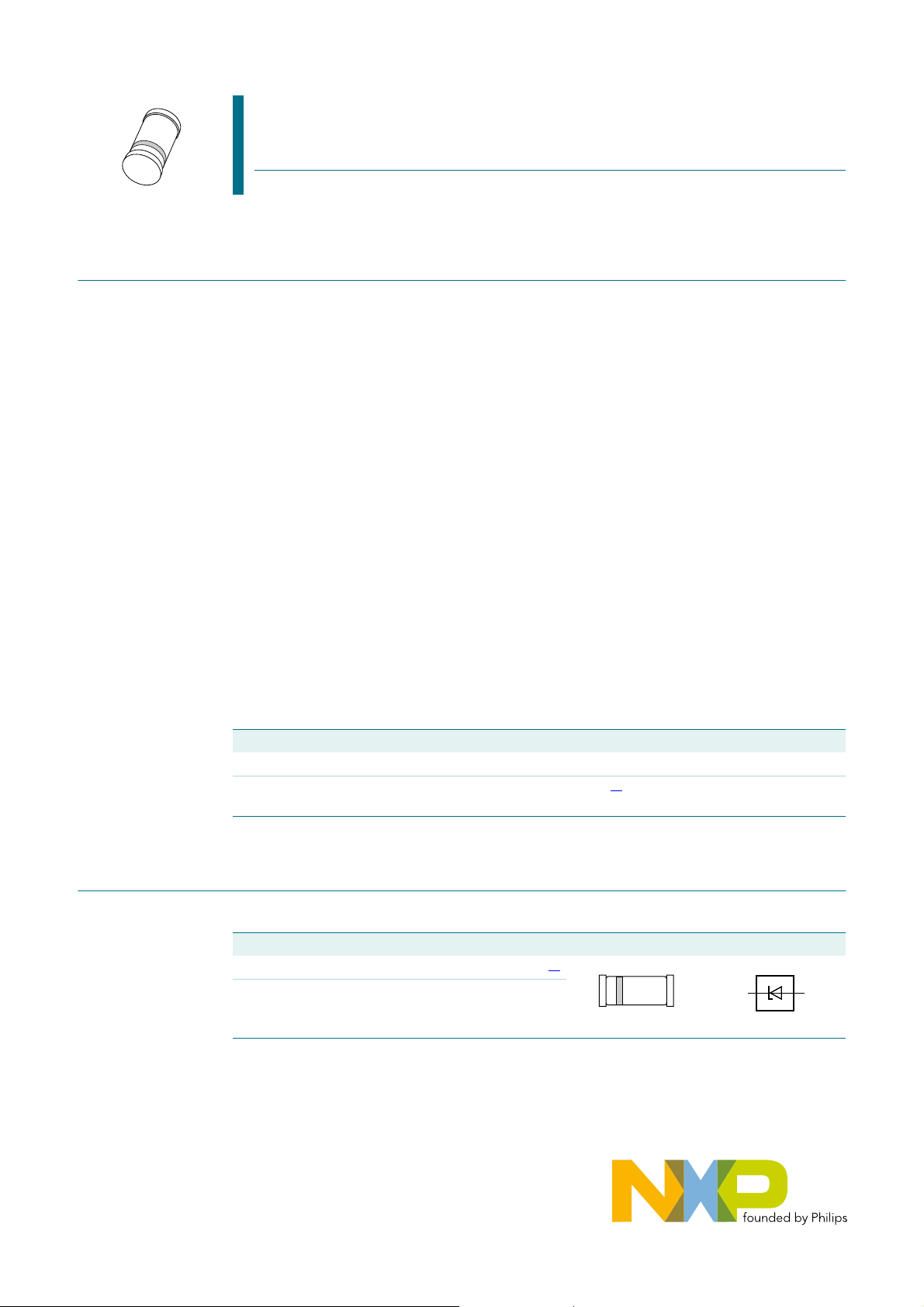
Low-power voltage regulator diodes in small hermetically sealed glass SOD80C
Surface-Mounted Device (SMD) packages. The diodes are available in the normalized
E24 ±2 % (BZV55-B) and approximately ±5 % (BZV55-C) tolerance range. The series
consists of 37 types with nominal working voltages from 2.4 V to 75 V.
1.2 Features
n Non-repetitive peak reverse power
dissipation: ≤ 40 W
n Total power dissipation: ≤ 500 mW n Low differential resistance
n Two tolerance series: ±2 % and ±5% n Small hermetically sealed glass SMD
1.3 Applications
n General regulation functions
1.4 Quick reference data
Table 1. Quick reference data
Symbol Parameter Conditions Min Typ Max Unit
V
F
P
ZSM
[1] tp= 100µs; square wave; Tj=25°C prior to surge
forward voltage IF= 10 mA - - 0.9 V
non-repetitive peak reverse
power dissipation
2. Pinning information
Table 2. Pinning
Pin Description Simplified outline Symbol
1 cathode
2 anode
n Wide working voltage range: nominal
2.4 V to 75 V (E24 range)
package
[1]
--40W
[1]
ka
1
006aaa152
2
[1] The marking band indicates the cathode.
Page 2

NXP Semiconductors
3. Ordering information
Table 3. Ordering information
Type number Package
BZV55-B2V4 to
BZV55-C75
[1] The series consists of 74 types with nominal working voltages from 2.4V to 75 V.
[1]
4. Marking
Table 4. Marking codes
Type number Marking code
BZV55-B2V4 to BZV55-C75 marking band
[1] blue: made in China
yellow: made in Philippines
BZV55 series
Voltage regulator diodes
Name Description Version
- hermetically sealed glass surface-mounted
package; 2 connectors
[1]
SOD80C
5. Limiting values
Table 5. Limiting values
In accordance with the Absolute Maximum Rating System (IEC 60134).
Symbol Parameter Conditions Min Max Unit
I
F
I
ZSM
forward current - 250 mA
non-repetitive peak reverse
current
P
ZSM
non-repetitive peak reverse
power dissipation
P
tot
T
stg
T
j
[1] tp= 100 µs; square wave; Tj=25°C prior to surge
[2] Device mounted on a ceramic substrate of 10 × 10 × 0.6 mm.
total power dissipation T
storage temperature −65 +200 °C
junction temperature −65 +200 °C
6. Thermal characteristics
Table 6. Thermal characteristics
Symbol Parameter Conditions Min Typ Max Unit
R
R
th(j-a)
th(j-t)
thermal resistance from
junction to ambient
thermal resistance from
junction to tie-point
≤ 50 °C
amb
≤ 50 °C
T
tp
in free air
[1]
- see
Table 8
and
9
[1]
-40W
[2]
- 400 mW
[2]
- 500 mW
[1]
- - 380 K/W
- - 300 K/W
[1] Device mounted on a ceramic substrate of 10 × 10 × 0.6 mm.
BZV55_SER_4 © NXP B.V. 2007. All rights reserved.
Product data sheet Rev. 04 — 19 July 2007 2 of 12
Page 3
NXP Semiconductors
BZV55 series
Voltage regulator diodes
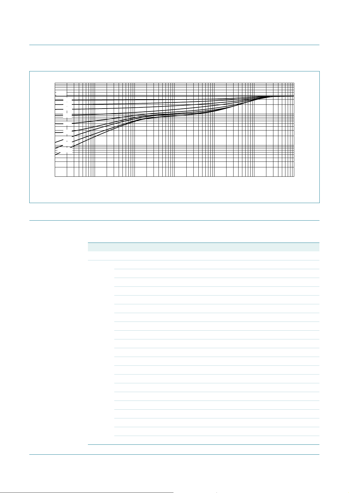
tp (ms)
006aab072
10
Z
th(j-a)
(K/W)
3
10
δ = 1
0.75
0.50
0.33
2
10
0.20
0.10
0.05
0.02
0.01
10
≤ 0.001
1
−1
10
110
2
10
3
10
4
10
Fig 1. Transient thermal impedance from junction to ambient as a function of pulse duration; typical values
7. Characteristics
Table 7. Characteristics
Tj=25°C unless otherwise specified.
Symbol Parameter Conditions Min Typ Max Unit
V
F
I
R
forward voltage IF= 10 mA - - 0.9 V
reverse current
BZV55-B/C2V4 V
BZV55-B/C2V7 V
BZV55-B/C3V0 V
BZV55-B/C3V3 V
BZV55-B/C3V6 V
BZV55-B/C3V9 V
BZV55-B/C4V3 V
BZV55-B/C4V7 V
BZV55-B/C5V1 V
BZV55-B/C5V6 V
BZV55-B/C6V2 V
BZV55-B/C6V8 V
BZV55-B/C7V5 V
BZV55-B/C8V2 V
BZV55-B/C9V1 V
BZV55-B/C10 V
BZV55-B/C11 V
BZV55-B/C12 V
BZV55-B/C13 V
BZV55-B/C15 to BZV55-B/C75 V
=1V --50µA
R
=1V --20µA
R
=1V --10µA
R
=1V --5µA
R
=1V --5µA
R
=1V --3µA
R
=1V --3µA
R
=2V --3µA
R
=2V --2µA
R
=2V --1µA
R
=4V --3µA
R
=4V --2µA
R
=5V --1µA
R
= 5 V - - 700 nA
R
= 6 V - - 500 nA
R
= 7 V - - 200 nA
R
= 8 V - - 100 nA
R
= 8 V - - 100 nA
R
= 8 V - - 100 nA
R
= 0.7V
R
Z(nom)
--50nA
5
BZV55_SER_4 © NXP B.V. 2007. All rights reserved.
Product data sheet Rev. 04 — 19 July 2007 3 of 12
Page 4

NXP Semiconductors
BZV55 series
Voltage regulator diodes
Table 8. Characteristics per type; BZV55-B2V4 to BZV55-C24
Tj=25°C unless otherwise specified.
BZV55-xxxSel Working
voltage
(V)
V
Z
IZ=5mA IZ=1mA IZ=5mA IZ=5mA
Min Max Typ Max Typ Max Min Typ Max Max Max
2V4 B 2.35 2.45 275 600 70 100 −3.5 −1.6 0 450 6.0
C 2.2 2.6
2V7 B 2.65 2.75 300 600 75 100 −3.5 −2.0 0 450 6.0
C 2.5 2.9
3V0 B 2.94 3.06 325 600 80 95 −3.5 −2.1 0 450 6.0
C 2.8 3.2
3V3 B 3.23 3.37 350 600 85 95 −3.5 −2.4 0 450 6.0
C 3.1 3.5
3V6 B 3.53 3.67 375 600 85 90 −3.5 −2.4 0 450 6.0
C 3.4 3.8
3V9 B 3.82 3.98 400 600 85 90 −3.5 −2.5 0 450 6.0
C 3.7 4.1
4V3 B 4.21 4.39 410 600 80 90 −3.5 −2.5 0 450 6.0
C 4.0 4.6
4V7 B 4.61 4.79 425 500 50 80 −3.5 −1.4 0.2 300 6.0
C 4.4 5.0
5V1 B 5.0 5.2 400 480 40 60 −2.7 −0.8 1.2 300 6.0
C 4.8 5.4
5V6 B 5.49 5.71 80 400 15 40 −2.0 1.2 2.5 300 6.0
C 5.2 6.0
6V2 B 6.08 6.32 40 150 6 10 0.4 2.3 3.7 200 6.0
C 5.8 6.6
6V8 B 6.66 6.94 30 80 6 15 1.2 3.0 4.5 200 6.0
C 6.4 7.2
7V5 B 7.35 7.65 30 80 6 15 2.5 4.0 5.3 150 4.0
C 7.0 7.9
8V2 B 8.04 8.36 40 80 6 15 3.2 4.6 6.2 150 4.0
C 7.7 8.7
9V1 B 8.92 9.28 40 100 6 15 3.8 5.5 7.0 150 3.0
C 8.5 9.6
10 B 9.8 10.2 50 150 8 20 4.5 6.4 8.0 90 3.0
C 9.4 10.6
11 B 10.8 11.2 50 150 10 20 5.4 7.4 9.0 85 2.5
C 10.4 11.6
12 B 11.8 12.2 50 150 10 25 6.0 8.4 10.0 85 2.5
C 11.4 12.7
BZV55_SER_4 © NXP B.V. 2007. All rights reserved.
Product data sheet Rev. 04 — 19 July 2007 4 of 12
Differential resistance
(Ω)
r
dif
Temperature
coefficient
(mV/K)
S
Z
Diode
capacitance
[1]
(pF)
C
d
Non-repetitive
peak reverse
current
ZSM
(A)
[2]
I
Page 5

NXP Semiconductors
BZV55 series
Voltage regulator diodes
Table 8. Characteristics per type; BZV55-B2V4 to BZV55-C24
…continued
Tj=25°C unless otherwise specified.
BZV55-xxxSel Working
voltage
V
(V)
Z
Differential resistance
r
(Ω)
dif
Temperature
coefficient
S
(mV/K)
Z
Diode
capacitance
d
(pF)
[1]
C
Non-repetitive
peak reverse
current
I
ZSM
IZ=5mA IZ=1mA IZ=5mA IZ=5mA
Min Max Typ Max Typ Max Min Typ Max Max Max
13 B 12.7 13.3 50 170 10 30 7.0 9.4 11.0 80 2.5
C 12.4 14.1
15 B 14.7 15.3 50 200 10 30 9.2 11.4 13.0 75 2.0
C 13.8 15.6
16 B 15.7 16.3 50 200 10 40 10.4 12.4 14.0 75 1.5
C 15.3 17.1
18 B 17.6 18.4 50 225 10 45 12.4 14.4 16.0 70 1.5
C 16.8 19.1
20 B 19.6 20.4 60 225 15 55 12.3 15.6 18.0 60 1.5
C 18.8 21.2
22 B 21.6 22.4 60 250 20 55 14.1 17.6 20.0 60 1.25
C 20.8 23.3
24 B 23.5 24.5 60 250 25 70 15.9 19.6 22.0 55 1.25
C 22.8 25.6
(A)
[2]
[1] f = 1 MHz; VR=0V
[2] tp= 100 µs; square wave; Tj=25°C prior to surge
BZV55_SER_4 © NXP B.V. 2007. All rights reserved.
Product data sheet Rev. 04 — 19 July 2007 5 of 12
Page 6

NXP Semiconductors
BZV55 series
Voltage regulator diodes
Table 9. Characteristics per type; BZV55-B27 to BZV55-C75
Tj=25°C unless otherwise specified.
BZV55-xxxSel Working
voltage
(V)
V
Z
IZ=2mA IZ= 0.5 mA IZ=2mA IZ=2mA
Min Max Typ Max Typ Max Min Typ Max Max Max
27 B 26.5 27.5 65 300 25 80 18.0 22.7 25.3 50 1.0
C 25.1 28.9
30 B 29.4 30.6 70 300 30 80 20.6 25.7 29.4 50 1.0
C 28.0 32.0
33 B 32.3 33.7 75 325 35 80 23.3 28.7 33.4 45 0.9
C 31.0 35.0
36 B 35.3 36.7 80 350 35 90 26.0 31.8 37.4 45 0.8
C 34.0 38.0
39 B 38.2 39.8 80 350 40 130 28.7 34.8 41.2 45 0.7
C 37.0 41.0
43 B 42.1 43.9 85 375 45 150 31.4 38.8 46.6 40 0.6
C 40.0 46.0
47 B 46.1 47.9 85 375 50 170 35.0 42.9 51.8 40 0.5
C 44.0 50.0
51 B 50.0 52.0 90 400 60 180 38.6 46.9 57.2 40 0.4
C 48.0 54.0
56 B 54.9 57.1 100 425 70 200 42.2 52.0 63.8 40 0.3
C 52.0 60.0
62 B 60.8 63.2 120 450 80 215 58.8 64.4 71.6 35 0.3
C 58.0 66.0
68 B 66.6 69.4 150 475 90 240 65.6 71.7 79.8 35 0.25
C 64.0 72.0
75 B 73.5 76.5 170 500 95 255 73.4 80.2 88.6 35 0.2
C 70.0 79.0
Differential resistance
(Ω)
r
dif
Temperature
coefficient
(mV/K)
S
Z
Diode
capacitance
[1]
(pF)
C
d
Non-repetitive
peak reverse
current
I
ZSM
(A)
[2]
[1] f = 1 MHz; VR=0V
[2] tp= 100 µs; square wave; Tj=25°C prior to surge
BZV55_SER_4 © NXP B.V. 2007. All rights reserved.
Product data sheet Rev. 04 — 19 July 2007 6 of 12
Page 7

NXP Semiconductors
BZV55 series
Voltage regulator diodes
tp (ms)
mbg801
10
P
ZSM
(W)
3
10
2
10
10
1
−1
10
(1)
(2)
1
(1) Tj=25°C (prior to surge)
(2) Tj= 150 °C (prior to surge)
Fig 2. Non-repetitive peak reverse power dissipation
as a function of pulse duration; maximum
values
mbg783
3V9
3V6
3V3
3V0
S
Z
(mV/K)
0
4V3
−1
−2
300
I
F
(mA)
200
100
0
0.6 10.8
mbg781
VF (V)
Tj=25°C
Fig 3. Forward current as a function of forward
voltage; typical values
mbg782
S
Z
(mV/K)
10
12
11
10
5
0
9V1
8V2
7V5
6V8
6V2
5V6
5V1
4V7
2V4
2V7
−3
060
20 40
I
Z
(mA)
BZV55-B/C2V4 to BZV55-B/C4V3
Tj=25°C to 150 °C
Fig 4. Temperature coefficient as a function of
working current; typical values
BZV55_SER_4 © NXP B.V. 2007. All rights reserved.
−5
02016
4812
I
Z
(mA)
BZV55-B/C4V7 to BZV55-B/C12
Tj=25°C to 150 °C
Fig 5. Temperature coefficient as a function of
working current; typical values
Product data sheet Rev. 04 — 19 July 2007 7 of 12
Page 8

NXP Semiconductors
8. Package outline
BZV55 series
Voltage regulator diodes
Hermetically sealed glass surface-mounted package; 2 connectors
ka
(1)
LL
H
DIMENSIONS (mm are the original dimensions)
UNIT
mm
Note
1. The marking band indicates the cathode.
D
1.60
1.45
OUTLINE
VERSION
SOD80C 100H01
H
3.7
3.3
L
0.3
REFERENCES
IEC JEDEC JEITA
D
0 1 2 mm
scale
EUROPEAN
PROJECTION
SOD80C
ISSUE DATE
05-01-26
06-03-16
Fig 6. Package outline SOD80C
9. Packing information
Table 10. Packing methods
The indicated -xxx are the last three digits of the 12NC ordering code.
Type number Package Description Packing quantity
BZV55-B2V4 to
BZV55-C75
[1] For further information and the availability of packing methods, seeSection 13.
[1]
2500 10000
SOD80C 4 mm pitch, 8 mm tape and reel -115 -135
BZV55_SER_4 © NXP B.V. 2007. All rights reserved.
Product data sheet Rev. 04 — 19 July 2007 8 of 12
Page 9

NXP Semiconductors
10. Soldering
Fig 7. Reflow soldering footprint SOD80C
BZV55 series
Voltage regulator diodes
4.55
4.30
2.30
solder lands
solder paste
1.601.702.25
0.90
(2x)
6.30
4.90
2.70
1.90
sod080c
solder resist
occupied area
Dimensions in mm
1.702.90
Fig 8. Wave soldering footprint SOD80C
solder lands
solder resist
occupied area
tracks
Dimensions in mm
sod080c
BZV55_SER_4 © NXP B.V. 2007. All rights reserved.
Product data sheet Rev. 04 — 19 July 2007 9 of 12
Page 10

NXP Semiconductors
BZV55 series
Voltage regulator diodes
11. Revision history
Table 11. Revision history
Document ID Release date Data sheet status Change notice Supersedes
BZV55_SER_4 20070719 Product data sheet CPCN200508022F BZV55_3
Modifications:
BZV55_3 20020228 Product specification - BZV55_2
BZV55_2 19990521 Product specification - BZV55_1
BZV55_1 19960426 Product specification - -
• The format of this data sheet has been redesigned to comply with the new identity guidelines
of NXP Semiconductors.
• Legal texts have been adapted to the new company name where appropriate.
• Section 4 “Marking”: enhanced as per CPCN200508022F
• Table 5: I
• Table 6: R
continuous forward current redefined to forward current
F
thermal resistance from junction to tie-point redefined to R
th(j-tp)
th(j-t)
• Figure 1: amended
• Section 9 “Packing information”: added
• Section 12 “Legal information”: updated
BZV55_SER_4 © NXP B.V. 2007. All rights reserved.
Product data sheet Rev. 04 — 19 July 2007 10 of 12
Page 11

NXP Semiconductors
12. Legal information
12.1 Data sheet status
BZV55 series
Voltage regulator diodes
Document status
Objective [short] data sheet Development This document contains data from the objective specification for product development.
Preliminary [short] data sheet Qualification This document contains data from the preliminary specification.
Product [short] data sheet Production This document contains the product specification.
[1] Please consult the most recently issued document before initiating or completing a design.
[2] The term ‘short data sheet’ is explained in section “Definitions”.
[3] The product status of device(s) described in this document may have changed since this document was published and may differ in case of multiple devices. The latest product status
information is available on the Internet at URL
[1][2]
Product status
12.2 Definitions
Draft — The document is a draft version only. The content is still under
internal review and subject to formal approval, which may result in
modifications or additions. NXP Semiconductors does not give any
representations or warranties as to the accuracy or completeness of
information included herein and shall haveno liability for the consequences of
use of such information.
Short data sheet — A short data sheet is an extract from a full data sheet
with the same product type number(s) and title.A short data sheet is intended
for quick referenceonly andshould notbe reliedupon tocontain detailedand
full information. For detailed and full information see the relevant full data
sheet, which is available on request via the local NXP Semiconductors sales
office. In case of any inconsistency or conflict with the short data sheet, the
full data sheet shall prevail.
12.3 Disclaimers
General — Information in this document is believed to be accurate and
reliable. However, NXP Semiconductors does not give any representations or
warranties, expressedor implied, asto theaccuracy or completeness ofsuch
information and shall have no liability for the consequences of use of such
information.
Right to make changes — NXP Semiconductors reserves the right to make
changes to information published in this document, including without
limitation specifications and product descriptions, at any time and without
notice. This document supersedes and replaces all informationsupplied prior
to the publication hereof.
Suitability for use — NXP Semiconductors products are not designed,
authorized or warranted to be suitable for use in medical, military, aircraft,
space or life support equipment, nor in applications where failure or
[3]
http://www.nxp.com.
Definition
malfunction of a NXPSemiconductors product can reasonably be expected to
result in personal injury, death or severe property or environmental damage.
NXP Semiconductors accepts no liability for inclusion and/or use of NXP
Semiconductors products in such equipment or applications and therefore
such inclusion and/or use is at the customer’s own risk.
Applications — Applications that are described herein for any of these
products are for illustrative purposes only. NXP Semiconductors makes no
representation or warranty that such applications will be suitable for the
specified use without further testing or modification.
Limiting values — Stress above one or more limiting values (as defined in
the Absolute Maximum Ratings System of IEC 60134)may cause permanent
damage to the device. Limiting values are stress ratings only and operation of
the device at these or any other conditions above those given in the
Characteristics sections of this document is not implied. Exposure to limiting
values for extended periods may affect device reliability.
Terms and conditions of sale — NXP Semiconductors products are sold
subject to the general terms and conditions of commercial sale, as published
at
http://www.nxp.com/profile/terms, including those pertaining to warranty,
intellectual property rights infringement and limitation of liability, unless
explicitly otherwise agreed to in writing by NXP Semiconductors. In case of
any inconsistency or conflict between information in this document and such
terms and conditions, the latter will prevail.
No offer to sell or license — Nothing in this document may be interpreted
or construed as an offer to sell products that is open for acceptance or the
grant, conveyanceor implication of any license under any copyrights, patents
or other industrial or intellectual property rights.
12.4 Trademarks
Notice: All referencedbrands, product names, service names and trademarks
are the property of their respective owners.
13. Contact information
For additional information, please visit: http://www.nxp.com
For sales office addresses, send an email to: salesaddresses@nxp.com
BZV55_SER_4 © NXP B.V. 2007. All rights reserved.
Product data sheet Rev. 04 — 19 July 2007 11 of 12
Page 12

NXP Semiconductors
14. Contents
1 Product profile . . . . . . . . . . . . . . . . . . . . . . . . . . 1
1.1 General description. . . . . . . . . . . . . . . . . . . . . . 1
1.2 Features . . . . . . . . . . . . . . . . . . . . . . . . . . . . . . 1
1.3 Applications . . . . . . . . . . . . . . . . . . . . . . . . . . . 1
1.4 Quick reference data. . . . . . . . . . . . . . . . . . . . . 1
2 Pinning information. . . . . . . . . . . . . . . . . . . . . . 1
3 Ordering information. . . . . . . . . . . . . . . . . . . . . 2
4 Marking . . . . . . . . . . . . . . . . . . . . . . . . . . . . . . . . 2
5 Limiting values. . . . . . . . . . . . . . . . . . . . . . . . . . 2
6 Thermal characteristics. . . . . . . . . . . . . . . . . . . 2
7 Characteristics. . . . . . . . . . . . . . . . . . . . . . . . . . 3
8 Package outline . . . . . . . . . . . . . . . . . . . . . . . . . 8
9 Packing information. . . . . . . . . . . . . . . . . . . . . . 8
10 Soldering . . . . . . . . . . . . . . . . . . . . . . . . . . . . . . 9
11 Revision history. . . . . . . . . . . . . . . . . . . . . . . . 10
12 Legal information. . . . . . . . . . . . . . . . . . . . . . . 11
12.1 Data sheet status . . . . . . . . . . . . . . . . . . . . . . 11
12.2 Definitions. . . . . . . . . . . . . . . . . . . . . . . . . . . . 11
12.3 Disclaimers . . . . . . . . . . . . . . . . . . . . . . . . . . . 11
12.4 Trademarks. . . . . . . . . . . . . . . . . . . . . . . . . . . 11
13 Contact information. . . . . . . . . . . . . . . . . . . . . 11
14 Contents . . . . . . . . . . . . . . . . . . . . . . . . . . . . . . 12
BZV55 series
Voltage regulator diodes
Please be aware that important notices concerning this document and the product(s)
described herein, have been included in section ‘Legal information’.
© NXP B.V. 2007. All rights reserved.
For more information, please visit: http://www.nxp.com
For sales office addresses, please send an email to: salesaddresses@nxp.com
Date of release: 19 July 2007
Document identifier: BZV55_SER_4
 Loading...