

BZB84 series
Dual Zener diodes
Rev. 03 — 9 June 2009 Product data sheet
1. Product profile
1.1 General description
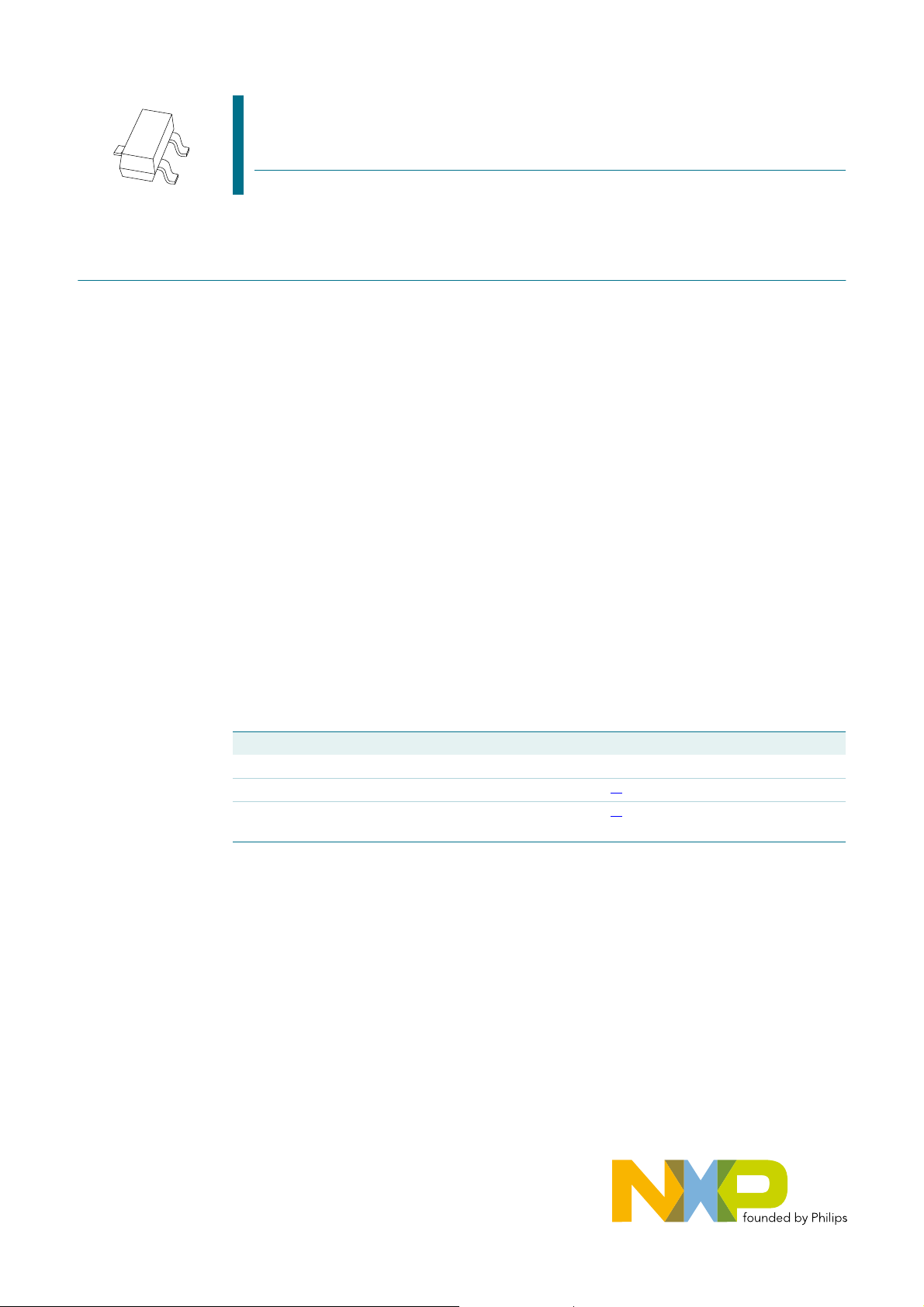
General-purpose Zener diodes in a SOT23 (TO-236AB) small Surface-Mounted
Device (SMD) plastic package.
1.2 Features
n Non-repetitive peak reverse power
dissipation: ≤ 40 W
n Total power dissipation: ≤ 300 mW n Dual common anode configuration
n Two tolerance series:
B=±2%andC=±5%
n Wide working voltage range:
nominal 2.4 V to 75 V (E24 range)
n Small plastic package suitable for
surface-mounted design
n AEC-Q101 qualified
1.3 Applications
n General regulation functions
1.4 Quick reference data
Table 1. Quick reference data
Symbol Parameter Conditions Min Typ Max Unit
Per diode
V
F
P
ZSM
[1] Pulse test: tp≤ 300 µs; δ≤0.02.
[2] tp= 100 µs; square wave; Tj=25°C prior to surge
forward voltage IF=10mA
non-repetitive peak reverse
power dissipation
[1]
- - 0.9 V
[2]
--40W
NXP Semiconductors
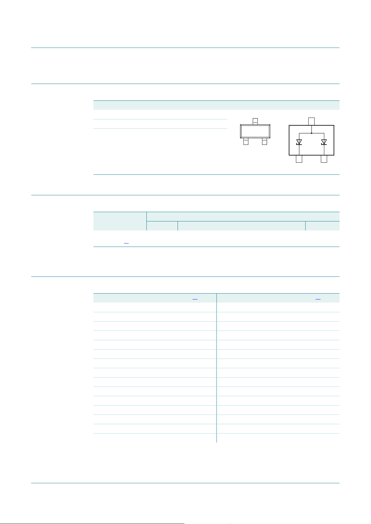
2. Pinning information
Table 2. Pinning
Pin Description Simplified outline Graphic symbol
1 cathode (diode 1)
2 cathode (diode 2)
3 common anode
3. Ordering information
Table 3. Ordering information
Type number Package
BZB84-B2V4 to
BZB84-C75
[1]
BZB84 series
Dual Zener diodes
3
12
Name Description Version
- plastic surface-mounted package; 3 leads SOT23
3
12
006aaa154
4. Marking
[1] The series consists of 74 types with nominal working voltages from 2.4 V to 75 V.
Table 4. Marking codes
Type number Marking code
BZB84-B2V4 V9* BZB84-C2V4 U9*
BZB84-B2V7 VA* BZB84-C2V7 UA*
BZB84-B3V0 VB* BZB84-C3V0 UB*
BZB84-B3V3 VC* BZB84-C3V3 UC*
BZB84-B3V6 VD* BZB84-C3V6 UD*
BZB84-B3V9 VE* BZB84-C3V9 UE*
BZB84-B4V3 VF* BZB84-C4V3 UF*
BZB84-B4V7 VG* BZB84-C4V7 UG*
BZB84-B5V1 VH* BZB84-C5V1 UH*
BZB84-B5V6 VK* BZB84-C5V6 UK*
BZB84-B6V2 VL* BZB84-C6V2 UL*
BZB84-B6V8 VM* BZB84-C6V8 UM*
BZB84-B7V5 VN* BZB84-C7V5 UN*
BZB84-B8V2 VP* BZB84-C8V2 UP*
BZB84-B9V1 VR* BZB84-C9V1 UR*
[1]
Type number Marking code
[1]
BZB84_SER_3 © NXP B.V. 2009. All rights reserved.
Product data sheet Rev. 03 — 9 June 2009 2 of 14

NXP Semiconductors
BZB84 series
Dual Zener diodes
Table 4. Marking codes
Type number Marking code
…continued
[1]
Type number Marking code
BZB84-B10 VS* BZB84-C10 US*
BZB84-B11 VT* BZB84-C11 UT*
BZB84-B12 VU* BZB84-C12 UU*
BZB84-B13 VV* BZB84-C13 UV*
BZB84-B15 VW* BZB84-C15 UW*
BZB84-B16 PT* BZB84-C16 PB*
BZB84-B18 PU* BZB84-C18 PC*
BZB84-B20 RP* BZB84-C20 RQ*
BZB84-B22 PV* BZB84-C22 PD*
BZB84-B24 PW* BZB84-C24 PE*
BZB84-B27 PX* BZB84-C27 PF*
BZB84-B30 PY* BZB84-C30 PG*
BZB84-B33 PZ* BZB84-C33 PH*
BZB84-B36 RA* BZB84-C36 PJ*
BZB84-B39 RB* BZB84-C39 PK*
BZB84-B43 RC* BZB84-C43 PL*
BZB84-B47 RD* BZB84-C47 PM*
BZB84-B51 RE* BZB84-C51 PN*
BZB84-B56 RF* BZB84-C56 PP*
BZB84-B62 RG* BZB84-C62 PQ*
BZB84-B68 RH* BZB84-C68 PR*
BZB84-B75 RJ* BZB84-C75 PS*
[1]
[1] * = -: made in Hong Kong
* = p: made in Hong Kong
* = t: made in Malaysia
* = W: made in China
5. Limiting values
Table 5. Limiting values
In accordance with the Absolute Maximum Rating System (IEC 60134).
Symbol Parameter Conditions Min Max Unit
Per diode
I
F
I
ZSM
P
ZSM
BZB84_SER_3 © NXP B.V. 2009. All rights reserved.
Product data sheet Rev. 03 — 9 June 2009 3 of 14
forward current - 200 mA
non-repetitive peak
reverse current
[1]
- see
Table 8, 9,
10 and 11
non-repetitive peak
[1]
-40W
reverse power dissipation

NXP Semiconductors
BZB84 series
Dual Zener diodes
Table 5. Limiting values
In accordance with the Absolute Maximum Rating System (IEC 60134).
Symbol Parameter Conditions Min Max Unit
Per device
P
tot
T
j
T
amb
T
stg
[1] tp= 100 µs; square wave; Tj=25°C prior to surge
[2] Device mounted on an FR4 Printed-Circuit Board (PCB), single-sided copper, tin-plated and standard
footprint.
total power dissipation T
junction temperature - 150 °C
ambient temperature −55 +150 °C
storage temperature −65 +150 °C
6. Thermal characteristics
Table 6. Thermal characteristics
Symbol Parameter Conditions Min Typ Max Unit
Per device; single diode loaded
R
th(j-a)
R
th(j-sp)
thermal resistance from
junction to ambient
thermal resistance from
junction to solder point
…continued
≤ 25 °C
amb
in free air
[2]
- 300 mW
[1]
- - 417 K/W
[2]
- - 100 K/W
[1] Device mounted on an FR4 PCB, single-sided copper, tin-plated and standard footprint.
[2] Soldering points at pins 1 and 2.
7. Characteristics
Table 7. Characteristics
Tj=25°C unless otherwise specified.
Symbol Parameter Conditions Min Typ Max Unit
Per diode
V
F
[1] Pulse test: tp≤ 300 µs; δ≤0.02.
forward voltage IF=10mA
[1]
- - 0.9 V
BZB84_SER_3 © NXP B.V. 2009. All rights reserved.
Product data sheet Rev. 03 — 9 June 2009 4 of 14

NXP Semiconductors
BZB84 series
Dual Zener diodes
Table 8. Characteristics per type; BZB84-B2V4 to BZB84-B24
Tj=25°C unless otherwise specified.
BZB84Bxxx
2V4 2.35 2.45 600 100 50 1 −3.5 0 450 6.0
2V7 2.65 2.75 600 100 20 1 −3.5 0 450 6.0
3V0 2.94 3.06 600 95 10 1 −3.5 0 450 6.0
3V3 3.23 3.37 600 95 5 1 −3.5 0 450 6.0
3V6 3.53 3.67 600 90 5 1 −3.5 0 450 6.0
3V9 3.82 3.98 600 90 3 1 −3.5 0 450 6.0
4V3 4.21 4.39 600 90 3 1 −3.5 0 450 6.0
4V7 4.61 4.79 500 80 3 2 −3.5 0.2 300 6.0
5V1 5.00 5.20 480 60 2 2 −2.7 1.2 300 6.0
5V6 5.49 5.71 400 40 1 2 −2.0 2.5 300 6.0
6V2 6.08 6.32 150 10 3 4 0.4 3.7 200 6.0
6V8 6.66 6.94 80 15 2 4 1.2 4.5 200 6.0
7V5 7.35 7.65 80 15 1 5 2.5 5.3 150 4.0
8V2 8.04 8.36 80 15 0.70 5 3.2 6.2 150 4.0
9V1 8.92 9.28 100 15 0.50 6 3.8 7.0 150 3.0
10 9.80 10.20 150 20 0.20 7 4.5 8.0 90 3.0
11 10.80 11.20 150 20 0.10 8 5.4 9.0 85 2.5
12 11.80 12.20 150 25 0.10 8 6.0 10.0 85 2.5
13 12.70 13.30 170 30 0.10 8 7.0 11.0 80 2.5
15 14.70 15.30 200 30 0.05 10.5 9.2 13.0 75 2.0
16 15.70 16.30 200 40 0.05 11.2 10.4 14.0 75 1.5
18 17.60 18.40 225 45 0.05 12.6 12.4 16.0 70 1.5
20 19.6 20.4 225 55 0.05 14.0 14.4 18.0 60 1.5
22 21.6 22.4 250 55 0.05 15.4 16.4 20.0 60 1.25
24 23.5 24.5 250 70 0.05 16.8 18.4 22.0 55 1.25
Working voltage
V
(V)
Z
Differential
resistance
(Ω)
r
dif
Reverse current
I
(µA)
R
Temperature
coefficient
(mV/K)
S
Z
Diode
capacitance
[1]
(pF)
C
d
Non-repetitive
peak reverse
current
I
ZSM
IZ=5mA IZ=1mA IZ=5mA IZ=5mA
Min Max Max Max Max VR(V) Min Max Max Max
(A)
[2]
[1] f = 1 MHz; VR=0V
[2] tp= 100 µs; square wave; Tj=25°C prior to surge
BZB84_SER_3 © NXP B.V. 2009. All rights reserved.
Product data sheet Rev. 03 — 9 June 2009 5 of 14

NXP Semiconductors
BZB84 series
Dual Zener diodes
Table 9. Characteristics per type; BZB84-B27 to BZB84-B75
Tj=25°C unless otherwise specified.
BZB84Bxxx
27 26.5 27.5 300 80 0.05 18.9 21.4 25.3 50 1.00
30 29.4 30.6 300 80 0.05 21.0 24.4 29.4 50 1.00
33 32.3 33.7 325 80 0.05 23.1 27.4 33.4 45 0.90
36 35.3 36.7 350 90 0.05 25.2 30.4 37.4 45 0.80
39 38.2 39.8 350 130 0.05 27.3 33.4 41.2 45 0.70
43 42.1 43.9 375 150 0.05 30.1 37.6 46.6 40 0.60
47 46.1 47.9 375 170 0.05 32.9 42.0 51.8 40 0.50
51 50.0 52.0 400 180 0.05 35.7 46.6 57.2 40 0.40
56 54.9 57.1 425 200 0.05 39.2 52.2 63.8 40 0.30
62 60.8 63.2 450 215 0.05 43.4 58.8 71.6 35 0.30
68 66.6 69.4 475 240 0.05 47.6 65.6 79.8 35 0.25
75 73.5 76.5 500 255 0.05 52.5 73.4 88.6 35 0.20
Working voltage
V
(V)
Z
Differential
resistance
(Ω)
r
dif
Reverse current
I
(µA)
R
Temperature
coefficient
(mV/K)
S
Z
Diode
capacitance
[1]
(pF)
C
d
Non-repetitive
peak reverse
current
I
ZSM
IZ=2mA IZ= 0.5 mA IZ=2mA IZ=2mA
Min Max Max Max Max VR(V) Min Max Max Max
(A)
[2]
[1] f = 1 MHz; VR=0V
[2] tp= 100 µs; square wave; Tj=25°C prior to surge
BZB84_SER_3 © NXP B.V. 2009. All rights reserved.
Product data sheet Rev. 03 — 9 June 2009 6 of 14

NXP Semiconductors
BZB84 series
Dual Zener diodes
Table 10. Characteristics per type; BZB84-C2V4 to BZB84-C24
Tj=25°C unless otherwise specified.
BZB84Cxxx
2V4 2.2 2.6 600 100 50 1 −3.5 0 450 6.0
2V7 2.5 2.9 600 100 20 1 −3.5 0 450 6.0
3V0 2.8 3.2 600 95 10 1 −3.5 0 450 6.0
3V3 3.1 3.5 600 95 5 1 −3.5 0 450 6.0
3V6 3.4 3.8 600 90 5 1 −3.5 0 450 6.0
3V9 3.7 4.1 600 90 3 1 −3.5 0 450 6.0
4V3 4.0 4.6 600 90 3 1 −3.5 0 450 6.0
4V7 4.4 5.0 500 80 3 2 −3.5 0.2 300 6.0
5V1 4.8 5.4 480 60 2 2 −2.7 1.2 300 6.0
5V6 5.2 6.0 400 40 1 2 −2.0 2.5 300 6.0
6V2 5.8 6.6 150 10 3 4 0.4 3.7 200 6.0
6V8 6.4 7.2 80 15 2 4 1.2 4.5 200 6.0
7V5 7.0 7.9 80 15 1 5 2.5 5.3 150 4.0
8V2 7.7 8.7 80 15 0.70 5 3.2 6.2 150 4.0
9V1 8.5 9.6 100 15 0.50 6 3.8 7.0 150 3.0
10 9.4 10.6 150 20 0.20 7 4.5 8.0 90 3.0
11 10.4 11.6 150 20 0.10 8 5.4 9.0 85 2.5
12 11.4 12.7 150 25 0.10 8 6.0 10.0 85 2.5
13 12.4 14.1 170 30 0.10 8 7.0 11.0 80 2.5
15 13.8 15.6 200 30 0.05 10.5 9.2 13.0 75 2.0
16 15.3 17.1 200 40 0.05 11.2 10.4 14.0 75 1.5
18 16.8 19.1 225 45 0.05 12.6 12.4 16.0 70 1.5
20 18.8 21.2 225 55 0.05 14.0 14.4 18.0 60 1.5
22 20.8 23.3 250 55 0.05 15.4 16.4 20.0 60 1.25
24 22.8 25.6 250 70 0.05 16.8 18.4 22.0 55 1.25
Working voltage
V
(V)
Z
Differential
resistance
(Ω)
r
dif
Reverse current
I
(µA)
R
Temperature
coefficient
(mV/K)
S
Z
Diode
capacitance
[1]
(pF)
C
d
Non-repetitive
peak reverse
current
I
ZSM
IZ=5mA IZ=1mA IZ=5mA IZ=5mA
Min Max Max Max Max VR(V) Min Max Max Max
(A)
[2]
[1] f = 1 MHz; VR=0V
[2] tp= 100 µs; square wave; Tj=25°C prior to surge
BZB84_SER_3 © NXP B.V. 2009. All rights reserved.
Product data sheet Rev. 03 — 9 June 2009 7 of 14

NXP Semiconductors
BZB84 series
Dual Zener diodes
Table 11. Characteristics per type; BZB84-C27 to BZB84-C75
Tj=25°C unless otherwise specified.
BZB84Cxxx
27 25.1 28.9 300 80 0.05 18.9 21.4 25.3 50 1.00
30 28.0 32.0 300 80 0.05 21.0 24.4 29.4 50 1.00
33 31.0 35.0 325 80 0.05 23.1 27.4 33.4 45 0.90
36 34.0 38.0 350 90 0.05 25.2 30.4 37.4 45 0.80
39 37.0 41.0 350 130 0.05 27.3 33.4 41.2 45 0.70
43 40.0 46.0 375 150 0.05 30.1 37.6 46.6 40 0.60
47 44.0 50.0 375 170 0.05 32.9 42.0 51.8 40 0.50
51 48.0 54.0 400 180 0.05 35.7 46.6 57.2 40 0.40
56 52.0 60.0 425 200 0.05 39.2 52.2 63.8 40 0.30
62 58.0 66.0 450 215 0.05 43.4 58.8 71.6 35 0.30
68 64.0 72.0 475 240 0.05 47.6 65.6 79.8 35 0.25
75 70.0 79.0 500 255 0.05 52.5 73.4 88.6 35 0.20
Working voltage
V
(V)
Z
Differential
resistance
(Ω)
r
dif
Reverse current
I
(µA)
R
Temperature
coefficient
(mV/K)
S
Z
Diode
capacitance
[1]
(pF)
C
d
Non-repetitive
peak reverse
current
I
ZSM
IZ=2mA IZ= 0.5 mA IZ=2mA IZ=2mA
Min Max Max Max Max VR(V) Min Max Max Max
(A)
[2]
[1] f = 1 MHz; VR=0V
[2] tp= 100 µs; square wave; Tj=25°C prior to surge
tp (ms)
mbg801
10
3
10
P
ZSM
(W)
2
10
10
1
−1
10
(1) Tj=25°C (prior to surge)
(2) Tj= 150 °C (prior to surge)
(1)
(2)
1
Fig 1. Per diode: Non-repetitive peak reverse power
dissipation as a function of pulse duration;
maximum values
300
I
F
(mA)
200
100
0
0.6 10.8
Tj=25°C
mbg781
VF (V)
Fig 2. Per diode: Forward current as a function of
forward voltage; typical values
BZB84_SER_3 © NXP B.V. 2009. All rights reserved.
Product data sheet Rev. 03 — 9 June 2009 8 of 14

NXP Semiconductors
BZB84 series
Dual Zener diodes
3V9
2V4
2V7
3V6
3V3
I
Z
mbg783
3V0
(mA)
0
S
Z
(mV/K)
−1
−2
−3
060
20 40
4V3
Tj=25°C to 150 °C
BZB84-B/C2V4 to BZB84-B/C4V3
Fig 3. Per diode: Temperature coefficient as a
function of working current; typical values
006aaa996
I
Z
(mA)
50
V
(V) = 2.7
Z(nom)
3.3
40
30
20
3.9
4.7
5.6 6.8 8.2
10
S
Z
(mV/K)
5
0
−5
02016
4812
12
11
10
9V1
8V2
7V5
6V8
6V2
5V6
5V1
4V7
mbg782
I
(mA)
Z
Tj=25°C to 150 °C
BZB84-B/C4V7 to BZB84-B/C12
Fig 4. Per diode: Temperature coefficient as a
function of working current; typical values
006aaa997
I
Z
(mA)
30
V
(V) = 10
Z(nom)
25
20
15
10
12
15
33272218
10
0
0108462
VZ (V)
Tj=25°C
BZB84-B/C2V7 to BZB84-B/C8V2
Fig 5. Per diode: Working current as a function of
working voltage; typical values
BZB84_SER_3 © NXP B.V. 2009. All rights reserved.
5
0
0403010 20
Tj=25°C
BZB84-B/C10 to BZB84-B/C36
Fig 6. Per diode: Working current as a function of
working voltage; typical values
36
V
(V)
Z
Product data sheet Rev. 03 — 9 June 2009 9 of 14

NXP Semiconductors
8. Test information
8.1 Quality information
This product has been qualified in accordance with the Automotive Electronics Council
(AEC) standard
suitable for use in automotive applications.
9. Package outline
BZB84 series
Dual Zener diodes
Q101 - Stress test qualification for discrete semiconductors
, and is
Fig 7. Package outline SOT23 (TO-236AB)
10. Packing information
Table 12. Packing methods
The indicated -xxx are the last three digits of the 12NC ordering code.
Type number Package Description Packing quantity
BZB84-B2V4 to
BZB84-C75
[2]
2.5
2.1
3.0
2.8
3
0.45
0.15
1.4
1.2
12
0.48
1.9
0.38
1.1
0.9
0.15
0.09
[1]
04-11-04Dimensions in mm
3000 10000
SOT23 4 mm pitch, 8 mm tape and reel -215 -235
[1] For further information and the availability of packing methods, seeSection 14.
[2] The series consists of 74 types with nominal working voltages from 2.4 V to 75 V.
BZB84_SER_3 © NXP B.V. 2009. All rights reserved.
Product data sheet Rev. 03 — 9 June 2009 10 of 14

NXP Semiconductors
11. Soldering
BZB84 series
Dual Zener diodes
3.3
2.9
1.9
solder lands
3
1.7
0.7
(3×)
0.5
(3×)
0.6
(3×)
1
0.6
(3×)
Fig 8. Reflow soldering footprint SOT23 (TO-236AB)
2.2
1.2
(2×)
1.4
(2×)
2
Dimensions in mm
solder resist
solder paste
occupied area
sot023_fr
solder lands
4.6
2.6
Dimensions in mm
1.4
preferred transport direction during soldering
2.8
4.5
solder resist
occupied area
sot023_fw
Fig 9. Wave soldering footprint SOT23 (TO-236AB)
BZB84_SER_3 © NXP B.V. 2009. All rights reserved.
Product data sheet Rev. 03 — 9 June 2009 11 of 14

NXP Semiconductors
BZB84 series
Dual Zener diodes
12. Revision history
Table 13. Revision history
Document ID Release date Data sheet status Change notice Supersedes
BZB84_SER_3 20090609 Product data sheet - BZB84_SER_2
Modifications:
• Table 5 “Limiting values”: P
• Table 6: R
maximum values amended
th
• Section 13 “Legal information”: updated
BZB84_SER_2 20090223 Product data sheet - BZB84_SER_1
BZB84_SER_1 20080514 Product data sheet - -
maximum value amended
tot
BZB84_SER_3 © NXP B.V. 2009. All rights reserved.
Product data sheet Rev. 03 — 9 June 2009 12 of 14

NXP Semiconductors
13. Legal information
13.1 Data sheet status
BZB84 series
Dual Zener diodes
Document status
Objective [short] data sheet Development This document contains data from the objective specification for product development.
Preliminary [short] data sheet Qualification This document contains data from the preliminary specification.
Product [short] data sheet Production This document contains the product specification.
[1] Please consult the most recently issued document before initiating or completing a design.
[2] The term ‘short data sheet’ is explained in section “Definitions”.
[3] The product status of device(s) described in this documentmay havechanged since this document was publishedand may differ in case of multiple devices.The latest productstatus
information is available on the Internet at URL
[1][2]
Product status
13.2 Definitions
Draft — The document is a draft version only. The content is still under
internal review and subject to formal approval, which may result in
modifications or additions. NXP Semiconductors does not give any
representations or warranties as to the accuracy or completeness of
information includedherein and shall haveno liability for the consequencesof
use of such information.
Short data sheet — A short data sheet is an extract from a full data sheet
with thesame product type number(s) andtitle. A short data sheet is intended
for quickreference only and should not be relied upon to contain detailed and
full information. For detailed and full information see the relevant full data
sheet, which is available on request via the local NXP Semiconductors sales
office. In case of any inconsistency or conflict with the short data sheet, the
full data sheet shall prevail.
13.3 Disclaimers
General — Information in this document is believed to be accurate and
reliable. However,NXP Semiconductors does not give any representationsor
warranties, expressedor implied, as to the accuracy or completenessof such
information and shall have no liability for the consequences of use of such
information.
Right to make changes — NXP Semiconductors reserves the right to make
changes to information published in this document, including without
limitation specifications and product descriptions, at any time and without
notice. This document supersedes andreplaces all information supplied prior
to the publication hereof.
Suitability for use — NXP Semiconductors products are not designed,
authorized or warranted to be suitable for use in medical, military, aircraft,
space or life support equipment, nor in applications where failure or
malfunction of an NXP Semiconductors product can reasonably be expected
to result in personal injury, death or severe property or environmental
[3]
http://www.nxp.com.
Definition
damage. NXP Semiconductors accepts no liability for inclusion and/or use of
NXP Semiconductors products in such equipment or applications and
therefore such inclusion and/or use is at the customer’s own risk.
Applications — Applications that are described herein for any of these
products are for illustrative purposes only. NXP Semiconductors makes no
representation or warranty that such applications will be suitable for the
specified use without further testing or modification.
Limiting values — Stress above one or more limiting values (as defined in
the Absolute Maximum RatingsSystem of IEC 60134) may cause permanent
damage to thedevice. Limiting values are stressratings only and operation of
the device at these or any other conditions above those given in the
Characteristics sections of this document is not implied. Exposure to limiting
values for extended periods may affect device reliability.
Terms and conditions of sale — NXP Semiconductors products are sold
subject to the general terms and conditions of commercial sale, as published
at
http://www.nxp.com/profile/terms, including those pertaining to warranty,
intellectual property rights infringement and limitation of liability, unless
explicitly otherwise agreed to in writing by NXP Semiconductors. In case of
any inconsistency or conflict between information in this document and such
terms and conditions, the latter will prevail.
No offer to sell or license — Nothing in this document may be interpreted
or construed as an offer to sell products that is open for acceptance or the
grant, conveyance or implication of any license under anycopyrights, patents
or other industrial or intellectual property rights.
Export control — This document as well as the item(s) described herein
may be subject to export control regulations. Export might require a prior
authorization from national authorities.
Quick reference data — The Quick reference data is an extract of the
product data given in the Limiting values and Characteristics sections of this
document, and as such is not complete, exhaustive or legally binding.
13.4 Trademarks
Notice: Allreferenced brands, productnames, service names and trademarks
are the property of their respective owners.
14. Contact information
For more information, please visit: http://www.nxp.com
For sales office addresses, please send an email to: salesaddresses@nxp.com
BZB84_SER_3 © NXP B.V. 2009. All rights reserved.
Product data sheet Rev. 03 — 9 June 2009 13 of 14

NXP Semiconductors
15. Contents
1 Product profile . . . . . . . . . . . . . . . . . . . . . . . . . . 1
1.1 General description. . . . . . . . . . . . . . . . . . . . . . 1
1.2 Features . . . . . . . . . . . . . . . . . . . . . . . . . . . . . . 1
1.3 Applications . . . . . . . . . . . . . . . . . . . . . . . . . . . 1
1.4 Quick reference data. . . . . . . . . . . . . . . . . . . . . 1
2 Pinning information. . . . . . . . . . . . . . . . . . . . . . 2
3 Ordering information. . . . . . . . . . . . . . . . . . . . . 2
4 Marking . . . . . . . . . . . . . . . . . . . . . . . . . . . . . . . . 2
5 Limiting values. . . . . . . . . . . . . . . . . . . . . . . . . . 3
6 Thermal characteristics. . . . . . . . . . . . . . . . . . . 4
7 Characteristics. . . . . . . . . . . . . . . . . . . . . . . . . . 4
8 Test information. . . . . . . . . . . . . . . . . . . . . . . . 10
8.1 Quality information . . . . . . . . . . . . . . . . . . . . . 10
9 Package outline . . . . . . . . . . . . . . . . . . . . . . . . 10
10 Packing information. . . . . . . . . . . . . . . . . . . . . 10
11 Soldering . . . . . . . . . . . . . . . . . . . . . . . . . . . . . 11
12 Revision history. . . . . . . . . . . . . . . . . . . . . . . . 12
13 Legal information. . . . . . . . . . . . . . . . . . . . . . . 13
13.1 Data sheet status . . . . . . . . . . . . . . . . . . . . . . 13
13.2 Definitions. . . . . . . . . . . . . . . . . . . . . . . . . . . . 13
13.3 Disclaimers . . . . . . . . . . . . . . . . . . . . . . . . . . . 13
13.4 Trademarks. . . . . . . . . . . . . . . . . . . . . . . . . . . 13
14 Contact information. . . . . . . . . . . . . . . . . . . . . 13
15 Contents . . . . . . . . . . . . . . . . . . . . . . . . . . . . . . 14
BZB84 series
Dual Zener diodes
Please be aware that important notices concerning this document and the product(s)
described herein, have been included in section ‘Legal information’.
© NXP B.V. 2009. All rights reserved.
For more information, please visit: http://www.nxp.com
For sales office addresses, please send an email to: salesaddresses@nxp.com
Date of release: 9 June 2009
Document identifier: BZB84_SER_3

 Loading...