

Page 1
SOT23
BF545A; BF545B; BF545C
N-channel silicon junction field-effect transistors
Rev. 4 — 15 September 2011 Product data sheet
1. Product profile
1.1 General description
N-channel symmetrical silicon junction field-effect transistors in a SOT23 package.
CAUTION
1.2 Features and benefits
This device is sensitive to ElectroStatic Discharge (ESD). Therefore care should be taken
during transport and handling.
Low leakage level (typ. 500 fA)
High gain
Low cut-off voltage (max. 2.2 V for BF545A).
1.3 Applications
Impedance converters in e.g. electret microphones and infra-red detectors
VHF amplifiers in oscillators and mixers.
1.4 Quick reference data
Table 1. Quick reference data
Symbol Parameter Conditions Min Typ Max Unit
V
V
I
DSS
P
y
DS
GSoff
tot
fs
drain-source voltage - - 30 V
gate-source cut-off
voltage
drain current VGS=0V; VDS=15V
total power dissipation T
forward transfer
admittance
ID=1A; VDS=15V 0.4 - 7.8 V
BF545A 2 - 6.5 mA
BF545B 6 - 15 mA
BF545C 12 - 25 mA
25 C--250mW
amb
VGS=0V; VDS=15V 3 - 6.5 mS
Page 2

NXP Semiconductors
12
3
sym054
d
sg
2. Pinning information
Table 2. Pinning
Pin Description Simplified outline Symbol
1 source (s)
2drain (d)
3gate (g)
3. Ordering information
Table 3. Ordering information
Type number Package
BF545A - plastic surface mounted package; 3 leads SOT23
BF545B
BF545C
BF545A; BF545B; BF545C
N-channel silicon junction field-effect transistors)
Name Description Version
4. Marking
Table 4. Marking
Type number Marking code
BF545A 20*
BF545B 21*
BF545C 22*
[1] * = p: made in Hong Kong.
* = t: made in Malaysia.
* = W: made in China.
[1]
BF545A_BF545B_BF545C All information provided in this document is subject to legal disclaimers. © NXP B.V. 2011. All rights reserved.
Product data sheet Rev. 4 — 15 September 2011 2 of 16
Page 3
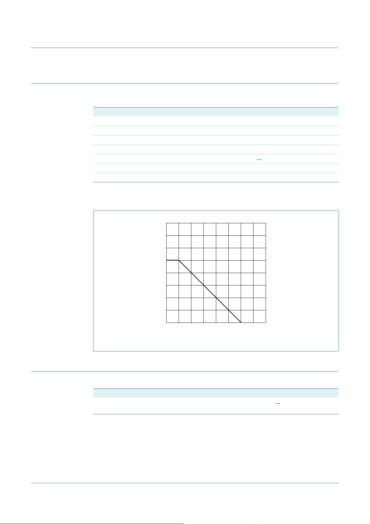
NXP Semiconductors
T
amb
(°C)
0 20015050 100
mbb688
200
100
300
400
P
tot
(mW)
0
5. Limiting values
Table 5. Limiting values
In accordance with the Absolute Maximum Rating System (IEC 60134).
Symbol Parameter Conditions Min Max Unit
V
DS
V
GSO
V
GDO
I
G
P
tot
T
stg
T
j
[1] Device mounted on an FR4 printed-circuit board, maximum lead length 4 mm; mounting pad for the drain
lead 10 mm
BF545A; BF545B; BF545C
N-channel silicon junction field-effect transistors)
drain-source voltage (DC) - 30 V
gate-source voltage open drain - 30 V
gate-drain voltage (DC) open source - 30 V
forward gate current (DC) - 10 mA
total power dissipation T
amb
25 C
storage temperature 65 +150 C
junction temperature - 150 C
2
.
[1]
-250mW
6. Thermal characteristics
BF545A_BF545B_BF545C All information provided in this document is subject to legal disclaimers. © NXP B.V. 2011. All rights reserved.
Product data sheet Rev. 4 — 15 September 2011 3 of 16
Fig 1. Power derating curve.
Table 6. Thermal characteristics
Symbol Parameter Conditions Typ Unit
R
th(j-a)
[1] Device mounted on an FR4 printed-circuit board, maximum lead length 4 mm; mou nting pad for the drain
thermal resistance from junction to
ambient
2
lead 10 mm
.
[1]
500 K/W
Page 4

NXP Semiconductors
7. Static characteristics
BF545A; BF545B; BF545C
N-channel silicon junction field-effect transistors)
Table 7. Static characteristics
Tj = 25 C unless otherwise specified.
Symbol Parameter Conditions Min Typ Max Unit
V
(BR)GSS
V
GSoff
gate-source breakdown voltage IG= 1 A; VDS=0V 30--V
gate-source cut-off voltage ID= 200 A; VDS=15V
BF545A 0.4 - 2.2 V
BF545B 1.6 - 3.8 V
BF545C 3.2 - 7.8 V
=1A; VDS=15V 0.4 - 7.5 V
I
D
I
DSS
drain current VGS=0V; VDS=15V
BF545A 2 - 6.5 mA
BF545B 6 - 15 mA
BF545C 12 - 25 mA
I
GSS
y
forward transfer admittance VGS=0V; VDS=15V 3 - 6.5 mS
fs
y
os
gate-source leakage current VGS= 20 V; VDS=0V - 0.5 1000 pA
--100 nA
common source output
= 20 V; VDS=0V;
V
GS
=125C
T
j
VGS=0V; VDS=15V - 40 - S
admittance
BF545A_BF545B_BF545C All information provided in this document is subject to legal disclaimers. © NXP B.V. 2011. All rights reserved.
Product data sheet Rev. 4 — 15 September 2011 4 of 16
Page 5
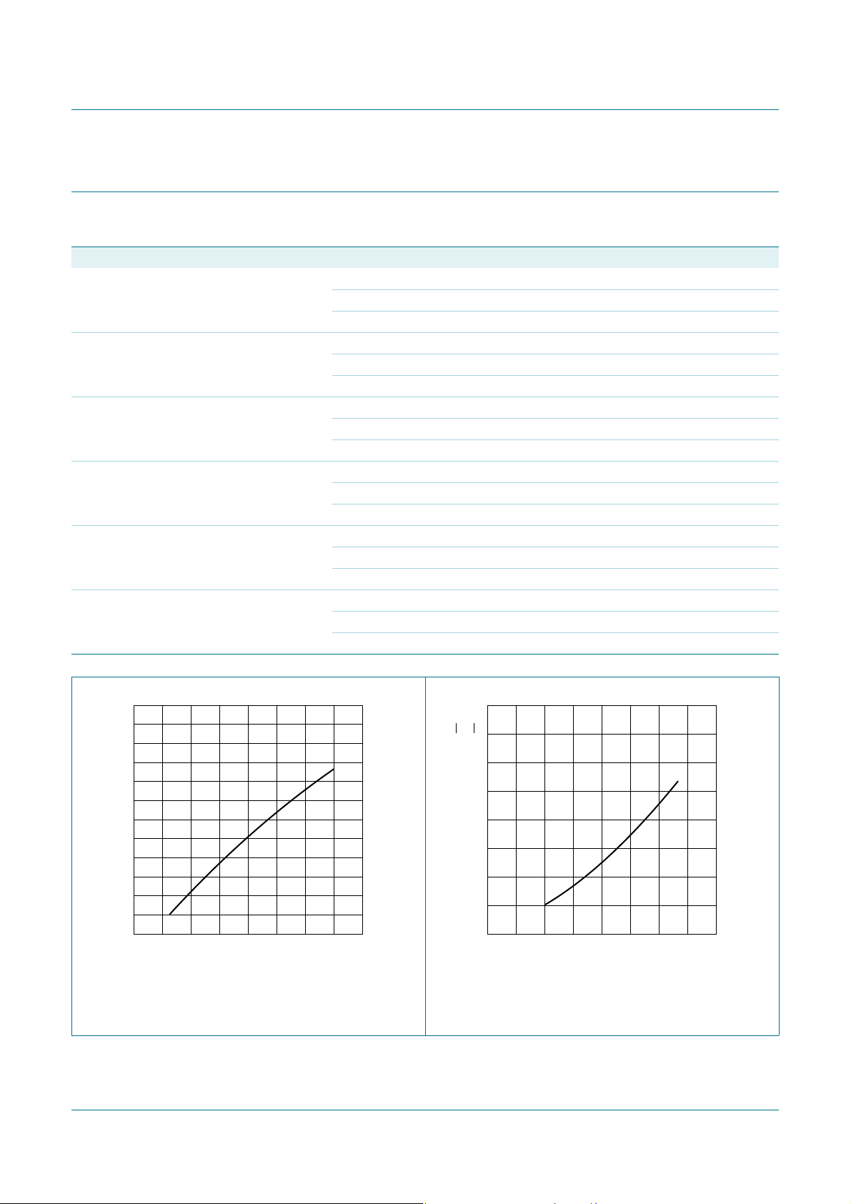
NXP Semiconductors
V
GSoff
(V)
0 −8−6−2 −4
mbb467
10
20
30
I
DSS
(mA)
0
V
GSoff
(V)
0 −8−6−2 −4
mbb466
5
4.5
5.5
6
Y
fs
(mS)
4
8. Dynamic characteristics
BF545A; BF545B; BF545C
N-channel silicon junction field-effect transistors)
Table 8. Dynamic characteristics
T
= 25 C unless otherwise specified.
amb
Symbol Parameter Conditions Min Typ Max Unit
C
iss
C
rss
g
is
input capacitance VDS=15V; f=1MHz
= 10 V - 1.7 - pF
V
GS
=0V - 3 - pF
V
GS
reverse transfer capacitance VDS=15V; f=1MHz
= 10 V - 0.8 - pF
V
GS
= 0 V - 0.9 - pF
V
GS
common source input
conductance
VDS=10V; ID=1mA
f = 100 MHz - 15 - S
f = 450 MHz - 300 - S
g
fs
common source transfer
conductance
VDS=10V; ID=1mA
f = 100 MHz - 2 - mS
f = 450 MHz - 1.8 - mS
g
rs
common source reverse
conductance
VDS=10V; ID=1mA
f = 100 MHz - 6- S
f = 450 MHz - 40 - S
g
os
common source output
conductance
VDS=10V; ID=1mA
f = 100 MHz - 30 - S
f = 450 MHz - 60 - S
VDS = 15 V; Tj = 25 C. VDS = 15 V; VGS = 0 V; Tj = 25 C.
Fig 2. Drain current as a function of gate-source
cut-off voltage; typical values.
Fig 3. Forward transfer admittance as a function of
gate-source cut-off voltage; typical values.
BF545A_BF545B_BF545C All information provided in this document is subject to legal disclaimers. © NXP B.V. 2011. All rights reserved.
Product data sheet Rev. 4 — 15 September 2011 5 of 16
Page 6
NXP Semiconductors
V
GSoff
(V)
0 −8−6−2 −4
mbb465
40
20
60
80
Y
os
(μS)
0
V
GSoff
(V)
0 −8−6−2 −4
mbb464
100
200
300
R
DSon
(Ω)
0
VDS (V)
0161248
mbb462
2
4
6
I
D
(mA)
0
(1)
(2)
(3)
VGS (V)
−30−1−2
mbb463
2
4
6
I
D
(mA)
0
VDS = 15 V; VGS = 0 V; Tj = 25 C. VDS = 100 mV; VGS = 0 V; Tj = 25 C.
Fig 4. Common-source output admittance as a
function of gate-source cut-off voltage; typical
values.
BF545A; BF545B; BF545C
N-channel silicon junction field-effect transistors)
Fig 5. Drain-source on-resistance as a function of
gate-source cut-off voltage; typical values.
BF545A
T
j
(1) V
GS
(2) V
GS
(3) V
Fig 6. Typical output characteristics. Fig 7. Typical input characteristics.
BF545A_BF545B_BF545C All information provided in this document is subject to legal disclaimers. © NXP B.V. 2011. All rights reserved.
Product data sheet Rev. 4 — 15 September 2011 6 of 16
GS
= 25 C.
= 0 V.
= 0.5 V.
= 1.0 V.
BF545A
= 15 V; Tj = 25 C.
V
DS
Page 7

NXP Semiconductors
VDS (V)
0161248
mbb460
8
4
12
16
I
D
(mA)
0
(1)
(6)
(2)
(3)
(4)
(5)
mbb459
VGS (V)
−60−2−4
8
4
12
16
I
D
(mA)
0
BF545A; BF545B; BF545C
N-channel silicon junction field-effect transistors)
BF545B
V
= 15 V; Tj = 25 C.
DS
(1) V
(2) V
(3) V
(4) V
(5) V
(6) V
BF545B
T
= 25 C.
j
= 0 V.
GS
= 0.5 V.
GS
= 1.0 V.
GS
= 1.5 V.
GS
= 2.0 V.
GS
= 2.5 V.
GS
Fig 8. Typical output characteristics. Fig 9. Typical input characteristics.
BF545A_BF545B_BF545C All information provided in this document is subject to legal disclaimers. © NXP B.V. 2011. All rights reserved.
Product data sheet Rev. 4 — 15 September 2011 7 of 16
Page 8

NXP Semiconductors
VDS (V)
0161248
mbb457
10
20
30
I
D
(mA)
0
(1)
(2)
(3)
(4)
(5)
(6)
VGS (V)
−80−2−6 −4
mbb456
10
20
30
I
D
(mA)
0
BF545A; BF545B; BF545C
N-channel silicon junction field-effect transistors)
(1) V
(2) V
(3) V
(4) V
(5) V
(6) V
BF545C
= 25 C.
T
j
= 0 V.
GS
= 1.0 V.
GS
= 2.0 V.
GS
= 3.0 V.
GS
= 4.0 V.
GS
= 5.0 V.
GS
BF545C
= 15 V; Tj = 25 C.
V
DS
Fig 10. Typical output characteristics. Fig 11. Typical input characteristics.
BF545A_BF545B_BF545C All information provided in this document is subject to legal disclaimers. © NXP B.V. 2011. All rights reserved.
Product data sheet Rev. 4 — 15 September 2011 8 of 16
Page 9

NXP Semiconductors
mbb461
VGS (V)
−30−1−2
1
10
−2
10
−1
10
2
10
10
3
I
D
(μA)
10
−3
mbb458
VGS (V)
−60−2−4
1
10
−2
10
−1
10
2
10
10
3
I
D
(μA)
10
−3
mbb455
1
10
−2
10
−1
10
2
10
10
3
I
D
(μA)
10
−3
VGS (V)
−80−2−6 −4
mbb454
−10
−1
−1
−10
−10
2
I
G
(pA)
−10
−2
VDG (V)
020168124
(3)
(4)
(2)
(1)
BF545A; BF545B; BF545C
N-channel silicon junction field-effect transistors)
BF545A
V
= 15 V; Tj = 25 C.
DS
Fig 12. Drain current as a function of gate-source
Fig 13. Drain current as a function of gate-source
voltage; typical values.
BF545C
= 15 V; Tj = 25 C.
V
DS
Fig 14. Drain current as a function of gate-source
voltage; typical values.
Fig 15. Gate current as a function of drain-gate
BF545B
VDS = 15 V; Tj = 25 C.
voltage; typical values.
I
= 10 mA only for BF545B and BF545C; Tj = 25 C.
D
= 10 mA.
(1) I
D
(2) I
= 1 mA.
D
= 0.1 mA.
(3) I
D
GSS
.
(4) I
voltage; typical values.
BF545A_BF545B_BF545C All information provided in this document is subject to legal disclaimers. © NXP B.V. 2011. All rights reserved.
Product data sheet Rev. 4 — 15 September 2011 9 of 16
Page 10

NXP Semiconductors
mbb453
−1
−10
−10
2
−10
3
I
GSS
(pA)
10
−1
Tj (°C)
−50 150100050
VGS (V)
−10 0−2−6 −4−8
mbb452
0.4
0.6
0.2
0.8
1
C
rss
(pF)
0
VGS (V)
−10 0−2−6 −4−8
mbb451
1
2
3
C
iss
(pF)
0
mbb468
f (MHz)
10 10
3
10
2
10
−1
1
10
10
2
y
is
(mS)
10
−2
(1)
(2)
VDS = 0 V; VGS = 20 V. VDS = 15 V; Tj = 25 C.
Fig 16. Gate current as a function of junction
temperature; typical values.
BF545A; BF545B; BF545C
N-channel silicon junction field-effect transistors)
Fig 17. Reverse transfer capacitance as a function of
gate-source voltage; typical values.
VDS = 15 V; Tj = 25 C. VDS = 10 V; ID = 1 mA; T
Fig 18. Typical input capacitance. Fig 19. Common-source input admittance; typical
BF545A_BF545B_BF545C All information provided in this document is subject to legal disclaimers. © NXP B.V. 2011. All rights reserved.
Product data sheet Rev. 4 — 15 September 2011 10 of 16
= 25 C.
amb
.
(1) b
is
(2) g
.
is
values.
Page 11

NXP Semiconductors
mbb469
10
1
10
2
Y
fs
(mS)
10
−1
f (MHz)
10 10
3
10
2
(2)
(1)
mbb470
f (MHz)
10 10
3
10
2
10
−2
10
−1
1
10
y
rs
(mS)
10
−3
(1)
(2)
mbb471
1
10
−1
10
y
os
(mS)
10
−2
f (MHz)
10 10
3
10
2
(1)
(2)
BF545A; BF545B; BF545C
N-channel silicon junction field-effect transistors)
VDS = 10 V; ID = 1 mA; T
(1) g
.
fs
(2) b
.
fs
Fig 20. Common-source forward transfer admittance;
= 25 C.
amb
Fig 21. Common-source reverse transfer admittance;
typical values.
VDS = 10 V; ID = 1 mA; T
(1) b
.
os
.
(2) g
os
Fig 22. Common-source output admittance; typical values.
amb
= 25 C.
V
= 10 V; ID = 1 mA; T
DS
(1) b
(2) g
.
rs
.
rs
typical values.
= 25 C.
amb
BF545A_BF545B_BF545C All information provided in this document is subject to legal disclaimers. © NXP B.V. 2011. All rights reserved.
Product data sheet Rev. 4 — 15 September 2011 11 of 16
Page 12

NXP Semiconductors
UNIT
A
1
max.
b
p
cD
E
e
1
H
E
L
p
Qwv
REFERENCES
OUTLINE
VERSION
EUROPEAN
PROJECTION
ISSUE DATE
04-11-04
06-03-16
IEC JEDEC JEITA
mm
0.1
0.48
0.38
0.15
0.09
3.0
2.8
1.4
1.2
0.95
e
1.9
2.5
2.1
0.55
0.45
0.1
0.2
DIMENSIONS (mm are the original dimensions)
0.45
0.15
SOT23 TO-236AB
b
p
D
e
1
e
A
A
1
L
p
Q
detail X
H
E
E
w M
v M
A
B
AB
0 1 2 mm
scale
A
1.1
0.9
c
X
12
3
Plastic surface-mounted package; 3 leads SOT23
BF545A; BF545B; BF545C
N-channel silicon junction field-effect transistors)
9. Package outline
Fig 23. Package outline.
BF545A_BF545B_BF545C All information provided in this document is subject to legal disclaimers. © NXP B.V. 2011. All rights reserved.
Product data sheet Rev. 4 — 15 September 2011 12 of 16
Page 13

NXP Semiconductors
BF545A; BF545B; BF545C
N-channel silicon junction field-effect transistors)
10. Revision history
Table 9. Revision history
Document ID Release date Data sheet status Change notice Supersedes
BF545A_BF545B_BF545C v.4 20110915 Product data sheet - BF545A_BF545B_BF545C v.3
Modifications:
BF545A_BF545B_BF545C v.3
(9397 750 13391)
BF545A-B-C v.2 19960729 Product specification - -
• The format of this data sheet has been redesigned to comply with the new identity
guidelines of NXP Semiconductors.
• Legal texts have been adapted to the new company name where appropriate.
• Package outline drawings have been updated to the latest version.
20040805 Product data sheet - BF545A-B-C v.2
BF545A_BF545B_BF545C All information provided in this document is subject to legal disclaimers. © NXP B.V. 2011. All rights reserved.
Product data sheet Rev. 4 — 15 September 2011 13 of 16
Page 14

NXP Semiconductors
BF545A; BF545B; BF545C
N-channel silicon junction field-effect transistors)
11. Legal information
11.1 Data sheet status
Document status
Objective [short] data sheet Development This document contains data from the objective specification for product development.
Preliminary [short] data sheet Qualification This document contains data from the preliminary specification.
Product [short] data sheet Production This document contains the product specification.
[1] Please consult the most recently issued document before initiating or completing a design.
[2] The term ‘short data sheet’ is explained in section “Definitions”.
[3] The product status of device(s) described in this docu ment may have change d since this d ocument was p ublished and may dif fer in case of multiple devices. The latest product statu s
information is available on the Internet at URL http://www.nxp.com.
[1][2]
Product status
[3]
Definition
11.2 Definitions
Draft — The document is a draft version only. The content is still under
internal review and subject to formal approval, which may result in
modifications or additions. NXP Semiconductors does not give any
representations or warranties as to the accuracy or completeness of
information included herein and shall have no liability for the consequences of
use of such information.
Short data sheet — A short data sheet is an extract from a full data sheet
with the same product type number(s) and title. A short data sheet is intended
for quick reference only and should not be relied upon to co nt ain det ailed and
full information. For detailed and full information see the relevant full data
sheet, which is available on request via the local NXP Semiconductors sales
office. In case of any inconsistency or conflict with the short data sheet, the
full data sheet shall prevail.
Product specification — The information and data provided in a Product
data sheet shall define the specification of the product as agreed between
NXP Semiconductors and its customer, unless NXP Semiconductors and
customer have explicitly agreed otherwise in writing. In no event however,
shall an agreement be valid in which the NXP Semiconductors product is
deemed to offer functions and qualities beyond those described in the
Product data sheet.
11.3 Disclaimers
Limited warranty and liability — Information in this document is believed to
be accurate and reliable. However, NXP Semiconductors does not give any
representations or warranties, expressed or implied, as to the accuracy or
completeness of such information and shall have no liability for the
consequences of use of such information.
In no event shall NXP Semiconductors be liable for any indirect, incidental,
punitive, special or consequential damages (including - without limitation - lost
profits, lost savings, business interruption, costs related to the removal or
replacement of any products or rework charges) whether or not such
damages are based on tort (including negligence), warranty, breach of
contract or any other legal theory.
Notwithstanding any damages that customer might incur for any reason
whatsoever, NXP Semi conductors’ aggregat e and cumulative liabil ity towards
customer for the products described herein shall be limited in accordance
with the Terms and conditions of commercial sale of NXP Semiconductors.
Right to make changes — NXP Semiconductors reserves the right to make
changes to information published in this document, including without
limitation specifications and product descriptions, at any time and without
notice. This document supersedes and replaces all information supplied prior
to the publication hereof.
Suitability for use — NXP Semiconductors products are not designed,
authorized or warranted to be suitable for use in life support, life-critical or
safety-critical systems or equipment, nor in applications where failure or
malfunction of an NXP Semiconductors product can reasonably be expected
to result in personal injury, death or severe property or environmental
damage. NXP Semiconductors accepts no liability for inclusion and/or use of
NXP Semiconductors products in such equipment or applications and
therefore such inclusion and/or use is at the customer’s own risk.
Applications — Applications that are described herein for any of these
products are for illustrative purposes only. NXP Semiconductors makes no
representation or warranty that such applications will be suitable for the
specified use without further testing or modification.
Customers are responsible for the design and operation of their applications
and products using NXP Semiconductors products, and NXP Semiconductors
accepts no liability for any assistance with applications or customer product
design. It is customer’s sole responsibility to determine whether the NXP
Semiconductors product is suitable and fit for the customer’s applications and
products planned, as well as for the planned application and use of
customer’s third party customer(s). Customers should provide appropriate
design and operating safeguards to minimize the risks associated with their
applications and products.
NXP Semiconductors does not accept any liability related to any default ,
damage, costs or problem which is based on any weakness or default in the
customer’s applications or products, or the application or use by customer’s
third party customer(s). Customer is responsible for doing all necessary
testing for the customer’s applications and products using NXP
Semiconductors products in order to avoid a default of the applications and
the products or of the application or use by customer’s third part y
customer(s). NXP does not accept any liability in this respect.
Limiting values — Stress above one or more limiting values (as defined in
the Absolute Maximum Ratings System of IEC 60134) will cause permanent
damage to the device. Limiting values are stress ratings only and (proper)
operation of the device at these or any other conditions above those given in
the Recommended operating conditions section (if present) or the
Characteristics sections of this document is not warranted. Constant or
repeated exposure to limiting values will permanently and irreversibly affect
the quality and reliability of the device.
Terms and conditions of commercial sale — NXP Semiconductors
products are sold subject to the general terms and conditions of commercial
sale, as published at http://www.nxp.com/profile/terms
agreed in a valid written individual agreement. In case an individual
agreement is concluded only the terms and conditions of the respective
agreement shall apply. NXP Semiconductors hereby expressly objects to
applying the customer’s general terms and conditions with regard to the
purchase of NXP Semiconductors products by customer.
No offer to sell or license — Nothing in this document may be interpreted or
construed as an offer to sell product s that is open for accept ance or the gr ant,
conveyance or implication of any license under any copyrights, patents or
other industrial or intellectual property rights.
Export control — This document as well as the item(s) described herein
may be subject to export control regulations. Export might require a prior
authorization from national authorities.
, unless otherwise
BF545A_BF545B_BF545C All information provided in this document is subject to legal disclaimers. © NXP B.V. 2011. All rights reserved.
Product data sheet Rev. 4 — 15 September 2011 14 of 16
Page 15

NXP Semiconductors
BF545A; BF545B; BF545C
N-channel silicon junction field-effect transistors)
Quick reference data — The Quick reference data is an extract of the
product data given in the Limiting values and Characteristics sections of this
document, and as such is not complete, exhaustive or legally binding.
Non-automotive qualified products — Unless this data sheet expressly
states that this specific NXP Semiconductors product is automotive qualified,
the product is not suitable for automotive use. It i s neit her qua lif ied nor tested
in accordance with automotive testing or application requirements. NXP
Semiconductors accepts no liability for inclusion and/or use of
non-automotive qualified products in automotive equipment or applications.
In the event that customer uses the product for design-in and use in
automotive applications to automotive specifications and standards, custome r
(a) shall use the product without NXP Semiconductors’ warranty of the
product for such automotive applications, use and specifications, and (b)
whenever customer uses the product for automotive applications beyond
NXP Semiconductors’ specifications such use shall be solely at customer’s
own risk, and (c) customer fully indemnifies NXP Semiconductors for any
liability, da mages or failed produ ct claims result ing from custome r design and
use of the product for automotive applications beyond NXP Semiconductors’
standard warranty and NXP Semiconductors’ product specifications.
11.4 Trademarks
Notice: All referenced brands, prod uct names, service names and trademarks
are the property of their respective owners.
12. Contact information
For more information, please visit: http://www.nxp.com
For sales office addresses, please send an email to: salesaddresses@nxp.com
BF545A_BF545B_BF545C All information provided in this document is subject to legal disclaimers. © NXP B.V. 2011. All rights reserved.
Product data sheet Rev. 4 — 15 September 2011 15 of 16
Page 16

NXP Semiconductors
13. Contents
1 Product profile . . . . . . . . . . . . . . . . . . . . . . . . . . 1
1.1 General description . . . . . . . . . . . . . . . . . . . . . 1
1.2 Features and benefits. . . . . . . . . . . . . . . . . . . . 1
1.3 Applications . . . . . . . . . . . . . . . . . . . . . . . . . . . 1
1.4 Quick reference data . . . . . . . . . . . . . . . . . . . . 1
2 Pinning information. . . . . . . . . . . . . . . . . . . . . . 2
3 Ordering information. . . . . . . . . . . . . . . . . . . . . 2
4 Marking. . . . . . . . . . . . . . . . . . . . . . . . . . . . . . . . 2
5 Limiting values. . . . . . . . . . . . . . . . . . . . . . . . . . 3
6 Thermal characteristics . . . . . . . . . . . . . . . . . . 3
7 Static characteristics. . . . . . . . . . . . . . . . . . . . . 4
8 Dynamic characteristics . . . . . . . . . . . . . . . . . . 5
9 Package outline . . . . . . . . . . . . . . . . . . . . . . . . 12
10 Revision history. . . . . . . . . . . . . . . . . . . . . . . . 13
11 Legal information. . . . . . . . . . . . . . . . . . . . . . . 14
11.1 Data sheet status . . . . . . . . . . . . . . . . . . . . . . 14
11.2 Definitions. . . . . . . . . . . . . . . . . . . . . . . . . . . . 14
11.3 Disclaimers. . . . . . . . . . . . . . . . . . . . . . . . . . . 14
11.4 Trademarks. . . . . . . . . . . . . . . . . . . . . . . . . . . 15
12 Contact information. . . . . . . . . . . . . . . . . . . . . 15
13 Contents . . . . . . . . . . . . . . . . . . . . . . . . . . . . . . 16
BF545A; BF545B; BF545C
N-channel silicon junction field-effect transistors)
Please be aware that important notices concerning this document and the product(s)
described herein, have been included in section ‘Legal information’.
© NXP B.V. 2011. All rights reserved.
For more information, please visit: http://www.nxp.com
For sales office addresses, please send an email to: salesaddresses@nxp.com
Document identifier: BF545A_BF545B_BF545C
Date of release: 15 September 2011
Page 17

 Loading...