

Page 1

BC817 series
45 V, 500 mA NPN general-purpose transistors
Rev. 7 — 18 June 2018 Product data sheet
1 Product profile
1.1 General description
NPN general-purpose transistors in a small SOT23 Surface-Mounted Device (SMD)
plastic package.
Table 1. Product overview
BC817 BC807
BC817-16 BC807-16
BC817-25 BC807-25
BC817-40
PackageType number
Nexperia JEDEC JEITA
SOT23 TO-236AB -
PNP complement
BC807-40
1.2 Features and benefits
• High current
• Three current gain selections
• AEC-Q101 qualified
1.3 Applications
• General-purpose switching and amplification
Page 2

Nexperia
1 2
3
sym123
C
E
B
BC817 series
45 V, 500 mA NPN general-purpose transistors
1.4 Quick reference data
Table 2. Quick reference data
T
= 25 °C unless otherwise specified.
amb
Symbol Parameter Conditions Min Typ Max Unit
V
CEO
I
C
I
CM
h
FE
[1] pulsed; tp ≤ 300 μs; δ ≤ 0.02
collector-emitter voltage open base - - 45 V
collector current - - 500 mA
peak collector current single pulse; tp ≤ 1 ms - - 1 A
BC817
BC817-16
BC817-25
BC817-40
VCE = 1 V; IC = 100 mA
[1]
100 - 600
[1]
100 - 250
[1]
160 - 400
[1]
250 - 600
2 Pinning information
Table 3. Pinning
Pin Symbol Description Simplified outline Graphic symbol
SOT23
1 B base
2 E emitter
3 C collector
3 Ordering information
Table 4. Ordering information
PackageType number
Name Description Version
BC817
BC817-16
BC817-25
BC817-40
TO-236AB Plastic surface-mounted package; 3 leads SOT23
BC817_SER All information provided in this document is subject to legal disclaimers. © Nexperia B.V. 2018. All rights reserved.
Product data sheet Rev. 7 — 18 June 2018
2 / 15
Page 3

Nexperia
BC817 series
45 V, 500 mA NPN general-purpose transistors
4 Marking
Table 5. Marking
Type number Marking code
BC817
BC817-16
BC817-25
BC817-40
[1] % = placeholder for manufacturing site code
[1]
6D%
[1]
6A%
[1]
6B%
[1]
6C%
5 Limiting values
Table 6. Limiting values
In accordance with the Absolute Maximum Rating System (IEC 60134).
Symbol Parameter Conditions Min Max Unit
V
V
V
I
I
I
T
T
T
CBO
CEO
EBO
C
CM
BM
tot
j
amb
stg
collector-base voltage open emitter - 50 V
collector-emitter voltage open base - 45 V
emitter-base voltage open collector - 5 V
collector current - 500 mA
peak collector current single pulse; tp ≤ 1 ms - 1 A
peak base current single pulse; tp ≤ 1 ms - 200 mA
[1] [2]
total power dissipation T
amb
≤ 25 °C
- 250 mWP
[3] [2]
- 345 mW
junction temperature - 150 °C
ambient temperature -65 150 °C
storage temperature -65 150 °C
[1] Device mounted on an FR4 Printed-Circuit-Board (PCB); single-sided copper; tin-plated and standard footprint.
[2] Valid for all available selection groups.
[3] Device mounted on an FR4 Printed-Circuit-Board (PCB); single-sided copper; tin-plated; mounting pad for collector 1 cm2.
BC817_SER All information provided in this document is subject to legal disclaimers. © Nexperia B.V. 2018. All rights reserved.
Product data sheet Rev. 7 — 18 June 2018
3 / 15
Page 4

Nexperia
T
amb
(°C)
-75 17512525 75-25
aaa-028120
200
100
300
400
P
tot
(mW)
0
(1)
(2)
BC817 series
45 V, 500 mA NPN general-purpose transistors
(1) FR4 PCB, single-sided copper; 1 cm
2
(2) FR4 PCB, single-sided copper; standard footprint
Figure 1. Power derating curves
BC817_SER All information provided in this document is subject to legal disclaimers. © Nexperia B.V. 2018. All rights reserved.
Product data sheet Rev. 7 — 18 June 2018
4 / 15
Page 5

Nexperia
aaa-028112
10
-5
1010
-2
10
-4
10
2
10
-1
tp (s)
10
-3
10
3
1
10
2
10
10
3
Z
th(j-a)
(K/W)
1
duty cycle = 1
0
0.01
0.02
0.05
0.10
0.20
0.33
0.50
0.75
aaa-028113
10
-5
1010
-2
10
-4
10
2
10
-1
tp (s)
10
-3
10
3
1
10
2
10
10
3
Z
th(j-a)
(K/W)
1
duty cycle = 1
0.01
0.02
0.05
0.10
0.20
0.33
0.50
0.75
0
BC817 series
45 V, 500 mA NPN general-purpose transistors
6 Thermal characteristics
Table 7. Thermal characteristics
Symbol Parameter Conditions Min Typ Max Unit
[1] [2]
th(j-a)
thermal resistance from junction
in free air
to ambient
[1] Device mounted on an FR4 Printed-Circuit-Board (PCB); single-sided copper; tin-plated and standard footprint.
[2] Valid for all available selection groups.
[3] Device mounted on an FR4 Printed-Circuit-Board (PCB); single-sided copper; tin-plated; mounting pad for collector 1 cm2 .
- - 500 K/WR
[3] [2]
- - 362 K/W
FR4 PCB; single-sided copper; tin-plated and standard footprint
Figure 2. Transient thermal impedance from junction to ambient as a function of pulse duration; typical values
FR4 PCB; single-sided copper; tin-plated; mounting pad for collector 1 cm
Figure 3. Transient thermal impedance from junction to ambient as a function of pulse duration; typical values
BC817_SER All information provided in this document is subject to legal disclaimers. © Nexperia B.V. 2018. All rights reserved.
Product data sheet Rev. 7 — 18 June 2018
2
5 / 15
Page 6

Nexperia
BC817 series
45 V, 500 mA NPN general-purpose transistors
7 Characteristics
Table 8. Characteristics
T
= 25 °C unless otherwise specified.
amb
Symbol Parameter Conditions Min Typ Max Unit
V
(BR)CBO
V
(BR)CEO
V
(BR)EBO
CBO
I
EBO
h
FE
h
FE
V
CEsat
V
BE
f
T
C
c
collector-base
IC = 100 µA; IE = 0 A 50 - - V
breakdown voltage
collector-emitter
IC = 10 mA; IB = 0 A 45 - - V
breakdown voltage
emitter-base
IE = 100 µA; IC = 0 A 5 - - V
breakdown voltage
collector-base
cut-off current
emitter-base
VCB = 20 V; IE = 0 A - - 100 nAI
VCB = 20 V; IE = 0 A; Tj = 150 °C - - 5 μA
VEB = 5 V; IC = 0 A - - 100 nA
cut-off current
DC current gain
BC817 VCE = 1 V; IC = 100 mA
BC817-16 VCE = 1 V; IC = 100 mA
BC817-25 VCE = 1 V; IC = 100 mA
BC817-40 VCE = 1 V; IC = 100 mA
DC current gain VCE = 1 V; IC = 500 mA
collector-emitter
IC = 500 mA; IB = 50 mA
[1]
[1]
[1]
[1]
[1]
[1]
100 - 600
100 - 250
160 - 400
250 - 600
40 - -
- - 700 mV
saturation voltage
base-emitter voltage VCE = 1 V; IC = 500 mA
[1] [2]
- - 1.2 V
transition frequency VCE = 5 V; IC = 10 mA; f = 100 MHz 100 - - MHz
collector capacitance VCB = 10 V; IE = ie = 0 A; f = 1 MHz - 3 - pF
[1] pulsed; tp ≤ 300 μs; δ ≤ 0.02
[2] VBE decreases by approxymately 2 mV/K with increasing temperature.
BC817_SER All information provided in this document is subject to legal disclaimers. © Nexperia B.V. 2018. All rights reserved.
Product data sheet Rev. 7 — 18 June 2018
6 / 15
Page 7

Nexperia
006aaa131
200
100
300
400
h
FE
0
IC(mA)
10
- 1
10
3
10
2
1 10
(1)
(2)
(3)
006aaa134
IC(mA)
10
- 1
10
3
10
2
1 10
1
10
V
BEsat
(V)
10
- 1
(1)
(2)
(3)
006aaa137
IC(mA)
10
- 1
10
3
10
2
1 10
10
- 1
1
V
CEsat
(V)
10
- 2
(1) (2)
(3)
VCE(V)
0 542 31
006aaa140
0.4
0.8
1.2
I
C
(A)
0
(6)
(7)
(8)
(9)
(10)
(1)(2)(3)(4)(5)
BC817 series
45 V, 500 mA NPN general-purpose transistors
VCE = -1 V
(1) T
(2) T
(3) T
= 150 °C
amb
= 25 °C
amb
= -55 °C
amb
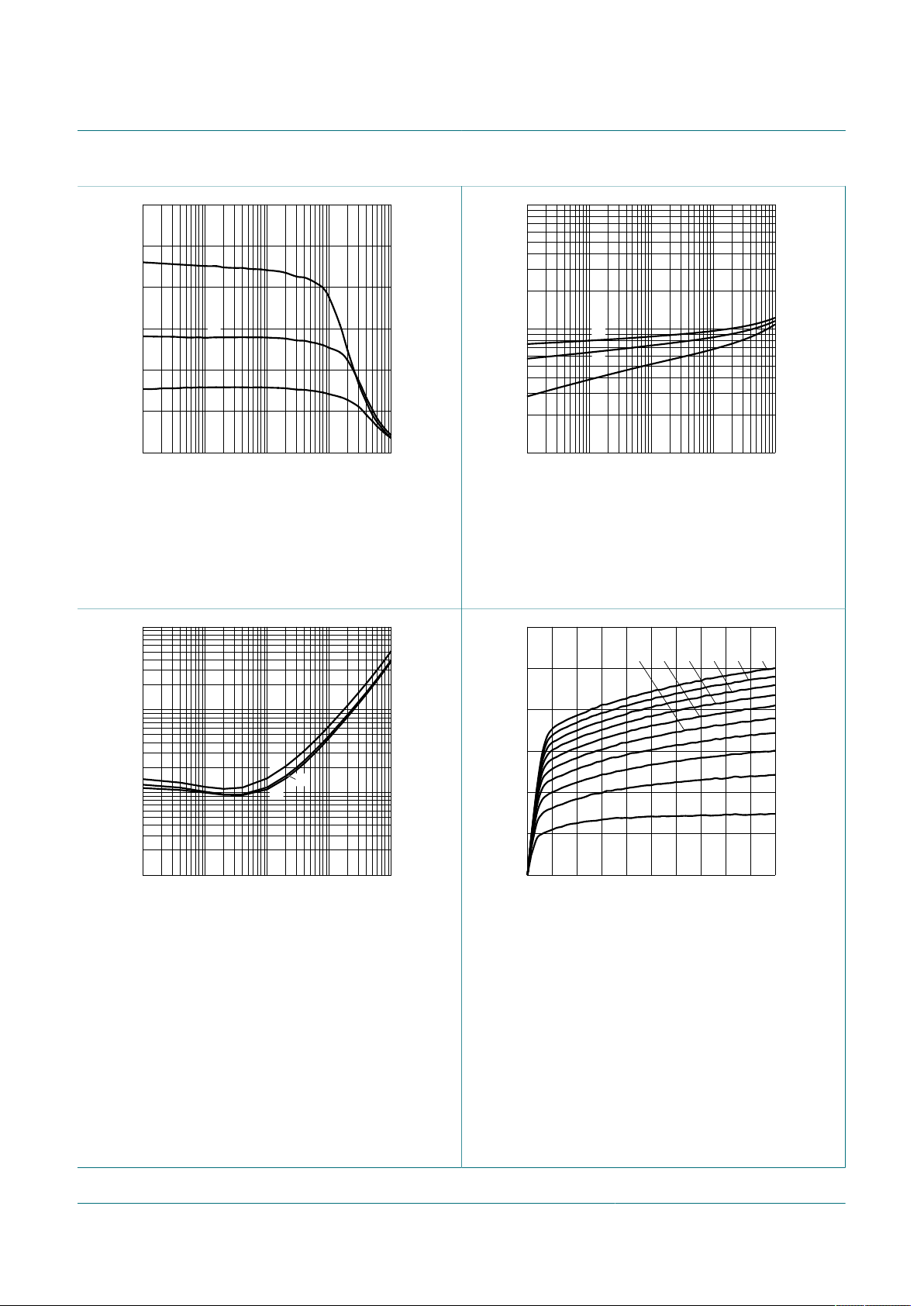
Figure 4. BC817-16: DC current gain as a function of
collector current; typical values
IC/IB = 10
(1) T
(2) T
(3) T
= 150 °C
amb
= 25 °C
amb
= -55 °C
amb
Figure 6. BC817-16: Collector-emitter saturation voltage
as a function of collector current; typical values
IC/IB = 10
(1) T
(2) T
(3) T
= -55 °C
amb
= 25 °C
amb
= 150 °C
amb
Figure 5. BC817-16: Base-emitter saturation voltage as
a function of collector current; typical values
T
= 25 °C
amb
(1) IB = -16.0 mA
(2) IB = -14.4 mA
(3) IB = -12.8 mA
(4) IB = -11.2 mA
(5) IB = -9.6 mA
(6) IB = -8.0 mA
(7) IB = -6.4 mA
(8) IB = -4.8 mA
BC817_SER All information provided in this document is subject to legal disclaimers. © Nexperia B.V. 2018. All rights reserved.
Product data sheet Rev. 7 — 18 June 2018
(9) IB = -3.2 mA
(10) IB = -1.6 mA
Figure 7. BC817-16: Collector current as a function of
collector-emitter voltage; typical values
7 / 15
Page 8
Nexperia
006aaa132
400
200
600
h
FE
0
IC(mA)
10
- 1
10
3
10
2
1 10
(1)
(2)
(3)
006aaa135
IC(mA)
10
- 1
10
3
10
2
1 10
1
10
V
BEsat
(V)
10
- 1
(1)
(2)
(3)
006aaa138
10
- 1
10
- 2
1
V
CEsat
(V)
10
- 3
IC(mA)
10
- 1
10
3
10
2
1 10
(1)
(2)
(3)
VCE(V)
0 542 31
006aaa141
0.4
0.8
1.2
I
C
(A)
0
(7)
(8)
(9)
(10)
(1)(2)(3)(4)(5)(6)
BC817 series
45 V, 500 mA NPN general-purpose transistors
VCE = 1 V
(1) T
(2) T
(3) T
= 150 °C
amb
= 25 °C
amb
= -55 °C
amb
Figure 8. BC817-25: DC current gain as a function of
collector current; typical values
IC/IB = 10
(1) T
(2) T
(3) T
= 150 °C
amb
= 25 °C
amb
= -55 °C
amb
Figure 10. BC817-25: Collector-emitter saturation
voltage as a function of collector current; typical values
IC/IB = 10
(1) T
(2) T
(3) T
= -55 °C
amb
= 25 °C
amb
= 150 °C
amb
Figure 9. BC817-25: Base-emitter saturation voltage as
a function of collector current; typical values
T
= 25 °C
amb
(1) IB = 13.0 mA
(2) IB = 11.7 mA
(3) IB = 10.4 mA
(4) IB = 9.1 mA
(5) IB = 7.8 mA
(6) IB = 6.5 mA
BC817_SER All information provided in this document is subject to legal disclaimers. © Nexperia B.V. 2018. All rights reserved.
Product data sheet Rev. 7 — 18 June 2018
(7) IB = 5.2 mA
(8) IB = 3.9 mA
(9) IB = 2.6 mA
(10) IB = 1.3 mA
Figure 11. BC817-25: Collector current as a function of
collector-emitter voltage; typical values
8 / 15
Page 9

Nexperia
006aaa133
400
200
600
800
h
FE
0
IC(mA)
10
- 1
10
3
10
2
1 10
(1)
(2)
(3)
006aaa136
IC(mA)
10
- 1
10
3
10
2
1 10
1
10
V
BEsat
(V)
10
- 1
(1)
(2)
(3)
006aaa139
10
- 1
10
- 2
1
V
CEsat
(V)
10
- 3
IC(mA)
10
- 1
10
3
10
2
1 10
(1)
(2)
(3)
VCE(V)
0 542 31
006aaa142
0.4
0.8
1.2
I
C
(A)
0
(7)
(8)
(9)
(10)
(1)(2)(3)(4)(5)(6)
BC817 series
45 V, 500 mA NPN general-purpose transistors
VCE = 1 V
(1) T
(2) T
(3) T
= 150 °C
amb
= 25 °C
amb
= -55 °C
amb
Figure 12. BC817-40: DC current gain as a function of
collector current; typical values
IC/IB = 10
(1) T
(2) T
(3) T
= 150 °C
amb
= 25 °C
amb
= -55 °C
amb
Figure 14. BC817-40: Collector-emitter saturation
voltage as a function of collector current; typical values
BC817_SER All information provided in this document is subject to legal disclaimers. © Nexperia B.V. 2018. All rights reserved.
Product data sheet Rev. 7 — 18 June 2018
IC/IB = 10
(1) T
(2) T
(3) T
= -55 °C
amb
= 25 °C
amb
= 150 °C
amb
Figure 13. BC817-40: Base-emitter saturation voltage as
a function of collector current; typical values
T
= 25 °C
amb
(1) IB = 12.0 mA
(2) IB = 10.8 mA
(3) IB = 9.6 mA
(4) IB = 8.4 mA
(5) IB = 7.2 mA
(6) IB = 6.0 mA
(7) IB = 4.8 mA
(8) IB = 3.6 mA
(9) IB = 2.4 mA
(10) IB = 1.2 mA
Figure 15. BC817-40: Collector current as a function of
collector-emitter voltage; typical values
9 / 15
Page 10
Nexperia
18-03-12Dimensions in mm
0.45
0.15
1.9
1.1
0.9
3.0
2.8
2.5
2.1
1.4
1.2
0.48
0.38
0.15
0.09
1 2
3
8 Test information
8.1 Quality information
This product has been qualified in accordance with the Automotive Electronics Council
(AEC) standard Q101 - Stress test qualification for discrete semiconductors, and is
suitable for use in automotive applications.
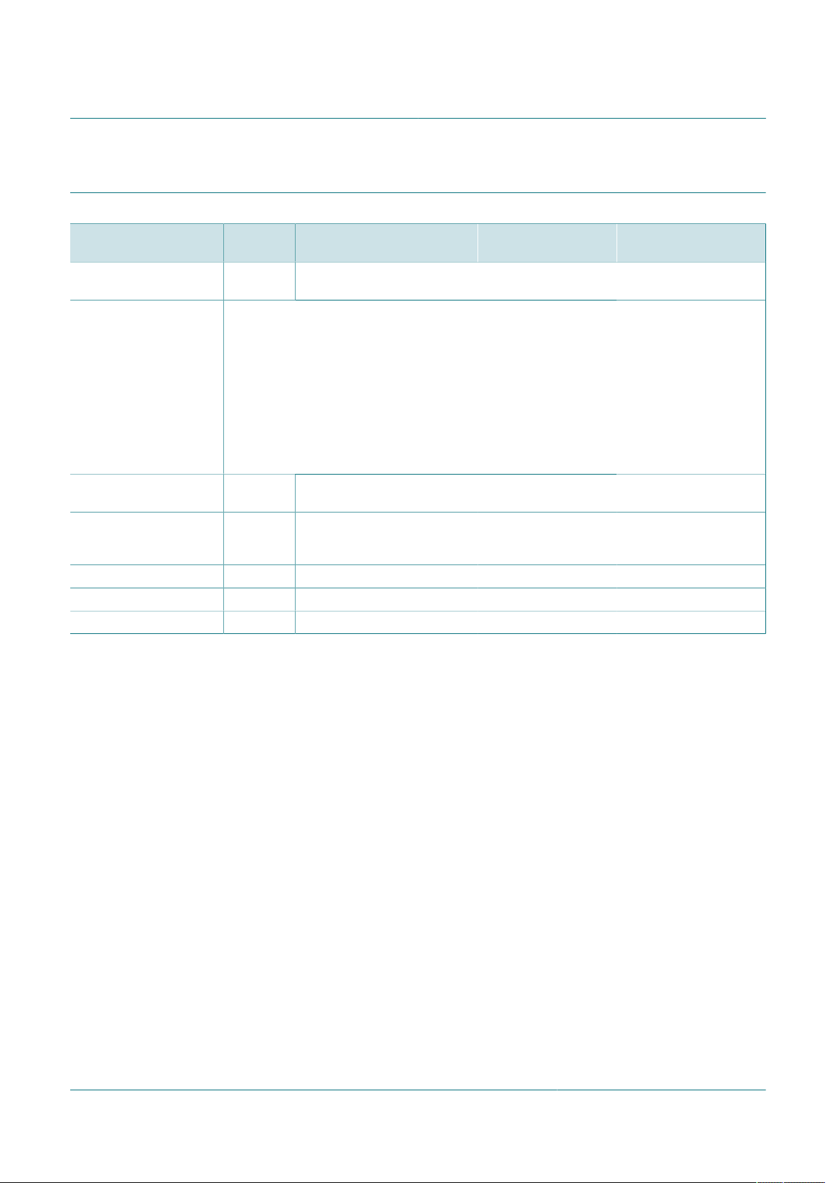
9 Package outline
Table 9. Package outline
BC817 series
45 V, 500 mA NPN general-purpose transistors
Figure 16. Package outline SOT23 (TO-236AB)
BC817_SER All information provided in this document is subject to legal disclaimers. © Nexperia B.V. 2018. All rights reserved.
Product data sheet Rev. 7 — 18 June 2018
10 / 15
Page 11

Nexperia
solder lands
solder resist
occupied area
solder paste
sot023_fr
0.5
(3×)
0.6
(3×)
0.6
(3×)
0.7
(3×)
3
1
3.3
2.9
1.7
1.9
2
Dimensions in mm
solder lands
solder resist
occupied area
preferred transport direction during soldering
sot023_fw
2.8
4.5
1.4
4.6
1.4
(2×)
1.2
(2×)
2.2
2.6
Dimensions in mm
10 Soldering
Table 10. Soldering
BC817 series
45 V, 500 mA NPN general-purpose transistors
Figure 17. Reflow soldering footprint for SOT23 (TO-236AB)
Figure 18. Wave soldering footprint for SOT23 (TO-236AB)
BC817_SER All information provided in this document is subject to legal disclaimers. © Nexperia B.V. 2018. All rights reserved.
Product data sheet Rev. 7 — 18 June 2018
11 / 15
Page 12
Nexperia
BC817 series
45 V, 500 mA NPN general-purpose transistors
11 Revision history
Table 11. Revision history
Document ID Release
date
BC817 v.7 20180618 Product data sheet - BC817_BC817W_BC337
Modifications: • The format of this data sheet has been redesigned to comply with the identity guidelines of
Nexperia.
• Legal texts have been adapted to the new company name where appropriate.
• Removed basic types: BC327 and BC807W (separate data sheet).
• Added Fig 1. Power derating curves in section "Limiting values" and the thermal graphs as
Fig 2. and Fig 3. in section "Thermal characteristics".
• Graphs in section "Characteristics" are sorted in new order.
• Added sections 8 "Test information" and 9 "Soldering".
• Removed Section "Packing information"
• AEC-Q101 qualified
BC817_BC817W_BC337
v.6
BC817_BC817W_BC337
v.5
BC817 v.4 20040116 Product Specification - BC817 v.3
BC817W_SER v.4 20040225 Product Specification - BC817W_SER v.3
BC337 v.3 19990415 Product Specification - BC337_338_CNV v.2
20091117 Product data sheet - BC817_BC817W_BC337
20050221 Product data sheet CPCN200302007F
Data sheet status Change notice Supersedes
v.6
v.5
BC817 v.4;
CPCN200405006F
BC817W_SER v.4;
BC337 v.3
BC817_SER All information provided in this document is subject to legal disclaimers. © Nexperia B.V. 2018. All rights reserved.
Product data sheet Rev. 7 — 18 June 2018
12 / 15
Page 13

Nexperia
12 Legal information
12.1 Data sheet status
BC817 series
45 V, 500 mA NPN general-purpose transistors
Document status
Objective [short] data sheet Development This document contains data from the objective specification for product
Preliminary [short] data sheet Qualification This document contains data from the preliminary specification.
Product [short] data sheet Production This document contains the product specification.
[1] Please consult the most recently issued document before initiating or completing a design.
[2] The term 'short data sheet' is explained in section "Definitions".
[3] The product status of device(s) described in this document may have changed since this document was published and may differ in case of multiple
devices. The latest product status information is available on the Internet at URL http://www.nexperia.com.
[1][2]
Product status
12.2 Definitions
Draft — The document is a draft version only. The content is still under
internal review and subject to formal approval, which may result in
modifications or additions. Nexperia does not give any representations or
warranties as to the accuracy or completeness of information included herein
and shall have no liability for the consequences of use of such information.
Short data sheet — A short data sheet is an extract from a full data sheet
with the same product type number(s) and title. A short data sheet is
intended for quick reference only and should not be relied upon to contain
detailed and full information. For detailed and full information see the
relevant full data sheet, which is available on request via the local Nexperia
sales office. In case of any inconsistency or conflict with the short data sheet,
the full data sheet shall prevail.
Product specification — The information and data provided in a Product
data sheet shall define the specification of the product as agreed between
Nexperia and its customer, unless Nexperia and customer have explicitly
agreed otherwise in writing. In no event however, shall an agreement be
valid in which the Nexperia product is deemed to offer functions and qualities
beyond those described in the Product data sheet.
12.3 Disclaimers
Limited warranty and liability — Information in this document is believed
to be accurate and reliable. However, Nexperia does not give any
representations or warranties, expressed or implied, as to the accuracy
or completeness of such information and shall have no liability for the
consequences of use of such information. Nexperia takes no responsibility
for the content in this document if provided by an information source outside
of Nexperia. In no event shall Nexperia be liable for any indirect, incidental,
punitive, special or consequential damages (including - without limitation lost profits, lost savings, business interruption, costs related to the removal
or replacement of any products or rework charges) whether or not such
damages are based on tort (including negligence), warranty, breach of
contract or any other legal theory. Notwithstanding any damages that
customer might incur for any reason whatsoever, Nexperia's aggregate and
cumulative liability towards customer for the products described herein shall
be limited in accordance with the Terms and conditions of commercial sale of
Nexperia.
Right to make changes — Nexperia reserves the right to make changes
to information published in this document, including without limitation
specifications and product descriptions, at any time and without notice. This
document supersedes and replaces all information supplied prior to the
publication hereof.
Applications — Applications that are described herein for any of these
products are for illustrative purposes only. Nexperia makes no representation
[3]
Definition
development.
or warranty that such applications will be suitable for the specified use
without further testing or modification. Customers are responsible for the
design and operation of their applications and products using Nexperia
products, and Nexperia accepts no liability for any assistance with
applications or customer product design. It is customer’s sole responsibility
to determine whether the Nexperia product is suitable and fit for the
customer’s applications and products planned, as well as for the planned
application and use of customer’s third party customer(s). Customers should
provide appropriate design and operating safeguards to minimize the risks
associated with their applications and products. Nexperia does not accept
any liability related to any default, damage, costs or problem which is based
on any weakness or default in the customer’s applications or products, or
the application or use by customer’s third party customer(s). Customer is
responsible for doing all necessary testing for the customer’s applications
and products using Nexperia products in order to avoid a default of the
applications and the products or of the application or use by customer’s third
party customer(s). Nexperia does not accept any liability in this respect.
Limiting values — Stress above one or more limiting values (as defined in
the Absolute Maximum Ratings System of IEC 60134) will cause permanent
damage to the device. Limiting values are stress ratings only and (proper)
operation of the device at these or any other conditions above those
given in the Recommended operating conditions section (if present) or the
Characteristics sections of this document is not warranted. Constant or
repeated exposure to limiting values will permanently and irreversibly affect
the quality and reliability of the device.
Terms and conditions of commercial sale — Nexperia products are
sold subject to the general terms and conditions of commercial sale, as
published at http://www.nexperia.com/profile/terms, unless otherwise agreed
in a valid written individual agreement. In case an individual agreement is
concluded only the terms and conditions of the respective agreement shall
apply. Nexperia hereby expressly objects to applying the customer’s general
terms and conditions with regard to the purchase of Nexperia products by
customer.
No offer to sell or license — Nothing in this document may be interpreted
or construed as an offer to sell products that is open for acceptance or
the grant, conveyance or implication of any license under any copyrights,
patents or other industrial or intellectual property rights.
Suitability for use in automotive applications — This Nexperia product
has been qualified for use in automotive applications. Unless otherwise
agreed in writing, the product is not designed, authorized or warranted to
be suitable for use in life support, life-critical or safety-critical systems or
equipment, nor in applications where failure or malfunction of an Nexperia
product can reasonably be expected to result in personal injury, death or
severe property or environmental damage. Nexperia and its suppliers accept
no liability for inclusion and/or use of Nexperia products in such equipment or
applications and therefore such inclusion and/or use is at the customer's own
risk.
BC817_SER All information provided in this document is subject to legal disclaimers. © Nexperia B.V. 2018. All rights reserved.
Product data sheet Rev. 7 — 18 June 2018
13 / 15
Page 14

Nexperia
BC817 series
45 V, 500 mA NPN general-purpose transistors
Quick reference data — The Quick reference data is an extract of the
product data given in the Limiting values and Characteristics sections of this
document, and as such is not complete, exhaustive or legally binding.
Export control — This document as well as the item(s) described herein
may be subject to export control regulations. Export might require a prior
authorization from competent authorities.
Translations — A non-English (translated) version of a document is for
reference only. The English version shall prevail in case of any discrepancy
between the translated and English versions.
12.4 Trademarks
Notice: All referenced brands, product names, service names and
trademarks are the property of their respective owners.
BC817_SER All information provided in this document is subject to legal disclaimers. © Nexperia B.V. 2018. All rights reserved.
Product data sheet Rev. 7 — 18 June 2018
14 / 15
Page 15

Nexperia
Contents
1 Product profile .................................................... 1
1.1 General description ............................................1
1.2 Features and benefits ........................................1
1.3 Applications ........................................................1
1.4 Quick reference data ......................................... 2
2 Pinning information ............................................ 2
3 Ordering information .......................................... 2
4 Marking .................................................................3
5 Limiting values ....................................................3
6 Thermal characteristics ...................................... 5
7 Characteristics .................................................... 6
8 Test information ................................................10
8.1 Quality information ...........................................10
9 Package outline .................................................10
10 Soldering ............................................................ 11
11 Revision history ................................................ 12
12 Legal information .............................................. 13
BC817 series
45 V, 500 mA NPN general-purpose transistors
Please be aware that important notices concerning this document and the product(s)
described herein, have been included in section 'Legal information'.
© Nexperia B.V. 2018. All rights reserved.
For more information, please visit: http://www.nexperia.com
For sales office addresses, please send an email to: salesaddresses@nexperia.com
Date of release: 18 June 2018
Document identifier: BC817_SER
 Loading...