

Page 1

DISCRETE SEMICONDUCTORS
DATA SH EET
ok, halfpage
M3D088
BAT54 series
Schottky barrier (double) diodes
Product specification
Supersedes data of 2001 Oct 12
2002 Mar 04
Page 2

Philips Semiconductors Product specification
Schottky barrier (double) diodes BAT54 series
FEATURES
• Low forward voltage
• Guard ring protected
• Small plastic SMD package.
APPLICATIONS
• Ultra high-speed switching
• Voltage clamping
• Protection circuits
• Blocking diodes.
DESCRIPTION
Planar Schottky barrier diodes encapsulated in a SOT23
small plastic SMD package. Single diodes and double
diodes with different pinning are available.
MARKING
TYPE NUMBER MARKING CODE
(1)
BAT54 L4∗
BAT54A L42 or ∗V3
BAT54C L43 or ∗W1
BAT54S L44 or ∗V4
Note
1. ∗ = p : Made in Hong Kong.
∗ = t : Made in Malaysia.
∗ = W: Made in China.
PINNING
DESCRIPTION
PIN
BAT54 BAT54A BAT54C BAT54S
3
a
1
a
2
k1,k
MGC421
1a k
2 n.c. k
3k a
handbook, 2 columns
Top view
1
2
1,a2
Fig.1 Simplified outline (SOT23) and pin
configuration.
3
12
n.c.
MLC357
(1) BAT54 (2) BAT54A
3
12
a
1
k
2
2
21
k1,a
2
3
MLC360
3
2002 Mar 04 2
12
MLC359
(3) BAT54C (4) BAT54S
12
Fig.2 Diode configuration and symbol.
MLC358
Page 3

Philips Semiconductors Product specification
Schottky barrier (double) diodes BAT54 series
LIMITING VALUES
In accordance with the Absolute Maximum Rating System (IEC 60134).
SYMBOL PARAMETER CONDITIONS MIN. MAX. UNIT
Per diode
V
R
I
F
I
FRM
I
FSM
T
stg
T
j
Per device
P
tot
THERMAL CHARACTERISTICS
continuous reverse voltage − 30 V
continuous forward current − 200 mA
repetitive peak forward current tp≤ 1s;δ≤0.5 − 300 mA
non-repetitive peak forward current tp<10ms − 600 mA
storage temperature −65 +150 °C
junction temperature − 125 °C
total power dissipation T
≤ 25 °C − 230 mW
amb
SYMBOL PARAMETER CONDITIONS VALUE UNIT
R
th j-a
thermal resistance from junction to
note 1 500 K/W
ambient
Note
1. Refer to SOT23 standard mounting conditions.
CHARACTERISTICS
T
=25°C unless otherwise specified.
amb
SYMBOL PARAMETER CONDITIONS MAX. UNIT
Per diode
V
F
I
R
t
rr
forward voltage see Fig.3
I
= 0.1 mA 240 mV
F
= 1 mA 320 mV
I
F
I
= 10 mA 400 mV
F
I
= 30 mA 500 mV
F
I
= 100 mA 800 mV
F
reverse current VR= 25 V; see Fig.4 2 µA
reverse recovery time when switched from IF=10mA
5ns
to IR= 10 mA; RL= 100 Ω;
measured at IR= 1 mA;
see Fig.6
C
d
diode capacitance f = 1 MHz; VR= 1 V; see Fig.5 10 pF
2002 Mar 04 3
Page 4

Philips Semiconductors Product specification
Schottky barrier (double) diodes BAT54 series
3
10
handbook, halfpage
I
F
(mA)
10
(1) T
(2) T
(3) T
10
10
2
1
1
amb
amb
amb
(3)(2)(1)
= 125°C.
=85°C.
=25°C.
(3)(2)(1)
VF (V)
Fig.3 Forward current as a function of forward
voltage; typical values.
MSA892
MSA893
(1)
(2)
I
(µA)
3
10
R
2
10
10
1
1
1.20.80.40
10
0102030
(1) T
(2) T
(3) T
amb
amb
amb
= 125°C.
=85°C.
=25°C.
(3)
V (V)
R
Fig.4 Reverse current as a function of reverse
voltage; typical values.
15
andbook, halfpage
C
d
(pF)
MSA891
10
5
0
0102030
f =1 MHz; T
amb
=25°C.
VR (V)
Fig.5 Diode capacitance as a function of reverse
voltage; typical values.
andbook, halfpage
I
F
I
R
Fig.6 Reverse recovery definitions.
dI
F
dt
t
10%
Q
r
90%
t
f
MRC129 - 1
2002 Mar 04 4
Page 5
Philips Semiconductors Product specification
Schottky barrier (double) diodes BAT54 series
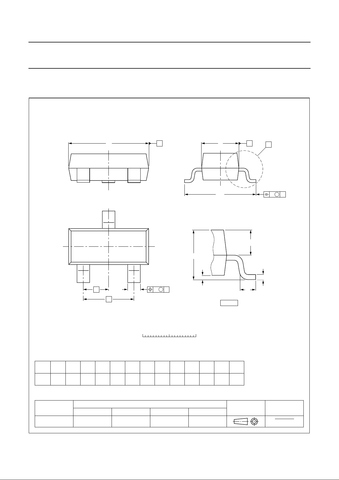
PACKAGE OUTLINE
Plastic surface mounted package; 3 leads SOT23
D
3
A
A
1
12
e
1
b
p
e
w M
B
E
H
E
detail X
AB
Q
L
p
X
v M
A
c
0 1 2 mm
scale
DIMENSIONS (mm are the original dimensions)
A
1
0.1
b
cD
p
0.48
0.15
0.09
3.0
2.8
0.38
IEC JEDEC EIAJ
e
E
1.4
1.9
1.2
REFERENCES
0.95
e
1
UNIT
A
max.
1.1
mm
0.9
OUTLINE
VERSION
SOT23 TO-236AB
2002 Mar 04 5
H
2.5
2.1
L
Qwv
p
E
0.55
0.45
0.15
0.45
0.2
0.1
EUROPEAN
PROJECTION
ISSUE DATE
97-02-28
99-09-13
Page 6

Philips Semiconductors Product specification
Schottky barrier (double) diodes BAT54 series
DATA SHEET STATUS
PRODUCT
DATA SHEET STATUS
Objective data Development This data sheet contains data from the objective specification for product
Preliminary data Qualification This data sheet contains data from the preliminary specification.
Product data Production This data sheet contains data from the product specification. Philips
(1)
STATUS
(2)
DEFINITIONS
development. Philips Semiconductors reserves the right to change the
specification in any manner without notice.
Supplementary data will be published at a later date. Philips
Semiconductors reserves the right to change the specification without
notice, in order to improve the design and supply the best possible
product.
Semiconductors reserves the right to make changes at any time in order
to improve the design, manufacturing and supply. Changes will be
communicated according to the Customer Product/Process Change
Notification (CPCN) procedure SNW-SQ-650A.
Notes
1. Please consult the most recently issued data sheet before initiating or completing a design.
2. The product status of the device(s) described in this data sheet may have changed since this data sheet was
published. The latest information is available on the Internet at URL http://www.semiconductors.philips.com.
DEFINITIONS
Short-form specification The data in a short-form
specification is extracted from a full data sheet with the
same type number and title. For detailed information see
the relevant data sheet or data handbook.
Limiting valuesdefinition Limitingvalues given arein
accordance with the Absolute Maximum Rating System
(IEC 60134). Stress above one or more of the limiting
values may cause permanent damage to the device.
These are stress ratings only and operation of the device
attheseoratanyotherconditions above those given in the
Characteristics sections of the specification is not implied.
Exposure to limiting values for extended periods may
affect device reliability.
Application information Applications that are
described herein for any of these products are for
illustrative purposes only. Philips Semiconductors make
norepresentation or warranty that such applications willbe
suitable for the specified use without further testing or
modification.
DISCLAIMERS
Life support applications These products are not
designed for use in life support appliances, devices, or
systems where malfunction of these products can
reasonably be expected to result in personal injury. Philips
Semiconductorscustomers using or selling these products
for use in such applications do so at their own risk and
agree to fully indemnify Philips Semiconductors for any
damages resulting from such application.
Right to make changes Philips Semiconductors
reserves the right to make changes, without notice, in the
products, including circuits, standard cells, and/or
software, described or contained herein in order to
improve design and/or performance. Philips
Semiconductors assumes no responsibility or liability for
theuseof any of these products, conveys no licence or title
under any patent, copyright, or mask work right to these
products,andmakesnorepresentationsorwarrantiesthat
these products are free from patent, copyright, or mask
work right infringement, unless otherwise specified.
2002 Mar 04 6
Page 7

Philips Semiconductors Product specification
Schottky barrier (double) diodes BAT54 series
NOTES
2002 Mar 04 7
Page 8

Philips Semiconductors – a w orldwide compan y
Contact information
For additional information please visit http://www.semiconductors.philips.com. Fax: +31 40 27 24825
For sales offices addresses send e-mail to: sales.addresses@www.semiconductors.philips.com.
© Koninklijke Philips Electronics N.V. 2002
All rights are reserved. Reproduction in whole or in part is prohibited without the prior written consent of the copyright owner.
The information presented in this document does not form part of any quotation or contract, is believed to be accurate and reliable and may be changed
without notice. No liability will be accepted by the publisher for any consequence of its use. Publication thereof does not convey nor imply any license
under patent- or other industrial or intellectual property rights.
Printed in The Netherlands 613514/04/pp8 Date of release: 2002 Mar 04 Document order number: 9397 750 09408
SCA74
 Loading...