

Page 1

AN13036
Introduction to Boundary Scan of LPC5500
Rev. 0 — 30 October 2020
1 Overview
This document focuses on the procedure of entering boundary scan mode for
the board-level test. It provides the setup sequence and script examples to
ensure first-pass success.
Engineers should understand the standard for the test access port and
boundary scan architecture from IEEE 1149.1.
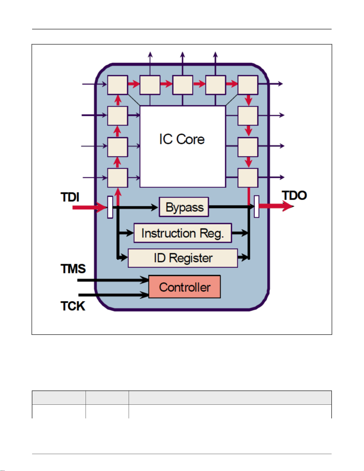
1.1 Boundary scan
Boundary scan is a method for testing interconnects on PCBs and internal IC
sub-blocks. It is defined in the IEEE 1149.1 standard.
In boundary scan test, each primary input and output signal on a device is
supplemented with a multi-purpose memory element called a boundary scan
cell. These cells are connected to a shift register, which is referred to as the
boundary scan register. This register can be used to read and write port states.
In normal mode, these cells are transparent, and the core is connected to the
ports. In boundary scan mode, the core is isolated from the ports and the port
signals are controlled by the JTAG interface.
Application Note
Contents
1 Overview......................................... 1
1.1 Boundary scan.............................1
1.2 JTAG Test Access Port (TAP)..... 2
1.3 BSDL introduction........................3
1.4 Downloading LPC55(S)xx BSDL
file................................................ 4
2 Setting up BSDL scan environment
........................................................ 4
2.1 JTAG tool.....................................4
2.2 Installing software........................ 4
2.3 Hardware connection diagram.....5
2.4 Setting LPC55(S)xx into boundary
scan mode................................... 6
3 BSDL file validation using JTAG Live
controller and JTAG Live Buzzer.... 7
3.1 Creating a new project by JTAG
Live Buzz..................................... 8
3.2 Infrastructure test.......................12
4 Reference......................................15
The following figure shows the principle of boundary scan chain.
Page 2
NXP Semiconductors
Overview
Figure 1. Boundary scan principle
1.2 JTAG Test Access Port (TAP)
The JTAG TAP is a general-purpose port and it can provide access to many test support functions built into the component. It has
four or five signals, as described in the following table. The TAP controller can be used for boundary scan as aforementioned by
using the JTAG pins.
Table 1. JTAG pin signal description
Signal Name I/O Type Description
TCK Input The test clock input provides the clock for the test logic.
Table continues on the next page...
Introduction to Boundary Scan of LPC5500, Rev. 0, 30 October 2020
Application Note 2 / 16
Page 3
NXP Semiconductors
Overview
Table 1. JTAG pin signal description (continued)
Signal Name I/O Type Description
TMS Input The value of the signal presented as TMS at the time of a rising edge at TCK
determines the next state of the TAP controller.
TDI Input Serial test instructions and data are received by the test logic.
TDO Output Serial output for test instructions and data from the test logic.
TRST_N Input Optional active low signal to reset the TAP controller.
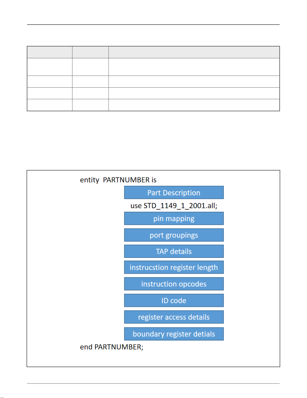
1.3 BSDL introduction
BSDL files are based on the syntax and grammar of VHDL (Very high-speed integrated-circuit Hardware Description Language).
They describe those aspects of the boundary scan implementation that are not defined by the standard. For example, it provides
the length of the instruction register (which is set by the device manufacturer), but not the length of the ID register (which the
standard mandates is 32 bits long). It gives information on which boundary scan cells connect to each pin, details of various
registers, and a description of the boundary scan cells themselves.
The following figure shows the main elements of a BSDL file (for simplicity, not all features are shown).
Figure 2. Main elements of a BSDL file
Introduction to Boundary Scan of LPC5500, Rev. 0, 30 October 2020
Application Note 3 / 16
Page 4
NXP Semiconductors
Setting up BSDL scan environment
For more details about BSDL, see https://www.xjtag.com/about-jtag/bsdl-files/bsdl-and-svf-file-formats/.
1.4 Downloading LPC55(S)xx BSDL file
Users can download BSDL files from the following links:
LPC55(S)6x: https://www.nxp.com/downloads/en/bsdl/LPC55S6X-BSDL.zip
LPC55(S)2x: https://www.nxp.com/downloads/en/bsdl/LPC55S2X-BSDL.zip
LPC55(S)1x: https://www.nxp.com/downloads/en/bsdl/LPC55S1X-BSDL.zip
For the latest part, users can download the BSDL file from “Design Tools & Files” item in the “Tools & Software” quick link on this
part’s dedicate website in nxp.com.
2 Setting up BSDL scan environment
2.1 JTAG tool
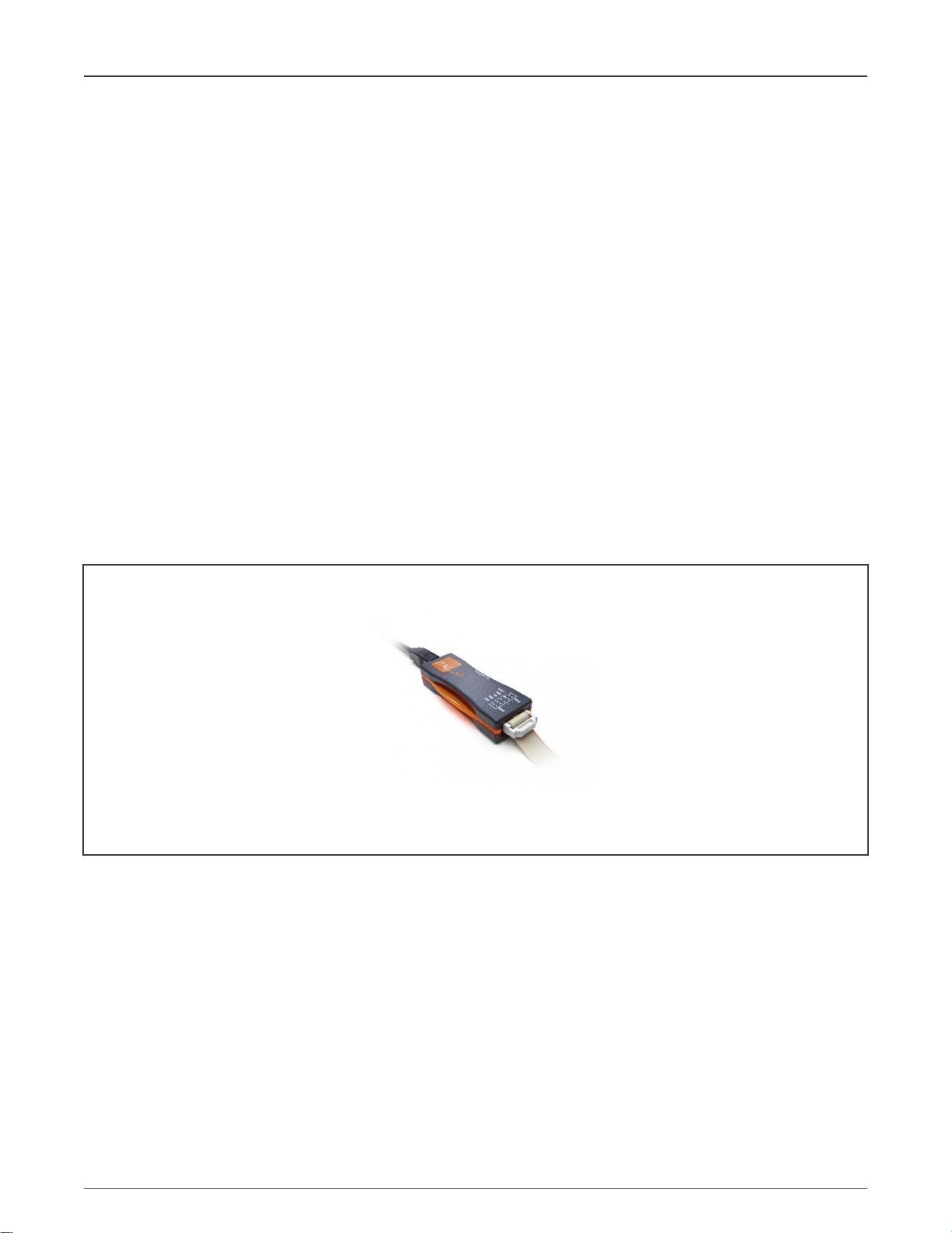
In this application note, JTAG Live controller is used, which is USB connected and powered and features a single test access port
in JTAG Technologies standard pin-out. It offers a maximum programable TCK speed of 6 MHz and features programmable output
voltage and input thresholds. Users can purchase JTAG Live controller through the following link:
https://www.jtaglive.com/product/low-cost-usb-jtag-live-controller-interface/
The following figure shows the JTAG Live controller.
Figure 3. JTAG Live Controller
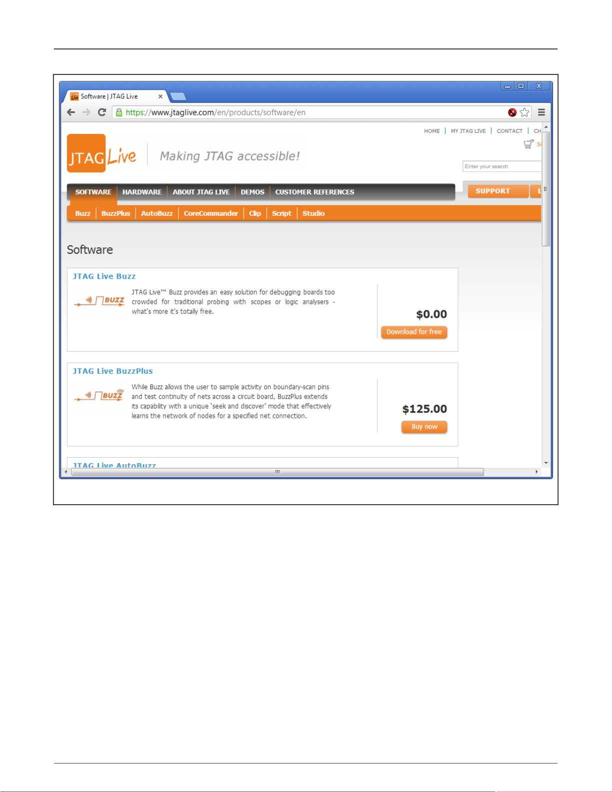
2.2 Installing software
The JTAG Live controller needs coordinate with PC software “JTAG Live Buzz”. The JTAG Live Buzz is downloadable from the
website JTAGLive.com.
The free software can be downloaded when the user provides registration to the site.
https://www.jtaglive.com/product/jtag-live-buzz/
Select the Download for free for the JTAG Live Buzz.
Introduction to Boundary Scan of LPC5500, Rev. 0, 30 October 2020
Application Note 4 / 16
Page 5
NXP Semiconductors
Setting up BSDL scan environment
Figure 4. Download JTAG Live Buzz
2.3 Hardware connection diagram
The JTAG Live controller consists of:
• Universal debugger hardware
• Debug cable specific to the processor architecture
The following figure shows the schematic diagram of hardware connection
Introduction to Boundary Scan of LPC5500, Rev. 0, 30 October 2020
Application Note 5 / 16
Page 6

NXP Semiconductors
Setting up BSDL scan environment
Figure 5. JTAG Live controller schematic diagram of hardware connection
Suggestions for users are as follows:
• To prevent the debuggers or target being damaged, it is forbidden to plug or unplug the debugger while the target is
powered on. The recommended sequence for powering on or off is as follows:
— Power on: debugger > target
— Power off: target > debugger
• The debugger interface has pin1. Please double check the direction to prevent damages to the debugger or target.
• It is recommended to press "Help->JTAG Training Center…" to enter the off-line help system to get basic training of JTAG
Live tool.
Take the LPC55S69-EVK board as an example:
1. Connect JTAG Live Controller to the EVK board by the 10 pin DuPont wires.
2. Connect to the PC through the USB cable.
3. Connect the EVK USB port to the PC.
2.4 Setting LPC55(S)xx into boundary scan mode
To set LPC55(S)xx into boundary scan mode, perform the following steps:
• Configure P0_2(TRST) = 1, P0_11(SWCLK) = 1 and PIO0_12 (SWDIO) = 0.
• Press and hold the "ISP(PIO0_5)" button (PIO0_5 = 0).
• Press and hold the "RESET" button (Reset = 0).
Introduction to Boundary Scan of LPC5500, Rev. 0, 30 October 2020
Application Note 6 / 16
Page 7

NXP Semiconductors
BSDL file validation using JTAG Live controller and JTAG Live Buzzer
• Release the "RESET" button (Reset = 1).
• Release "ISP" button (PIO0_5 = 1).
JTAG functions TRST, TCK, TMS, TDI, and TDO are selected on pins PIO0_2 to PIO0_6 by hardware when the LPC55(S)xx parts
are in boundary scan mode.
Now LPC55(S)xx enters boundary scan mode.
3 BSDL file validation using JTAG Live controller and JTAG Live Buzzer
When the JTAG Live controller is connected with the PC successfully, the “USB Serial Converter” should appear in the Device
Manager, as shown in the following figure.
Figure 6. JTAG Live name appearing in Device Manager
Open the JTAG Live software and choose "JTAG Live".
Introduction to Boundary Scan of LPC5500, Rev. 0, 30 October 2020
Application Note 7 / 16
Page 8

NXP Semiconductors
BSDL file validation using JTAG Live controller and JTAG Live Buzzer
Figure 7. JTAG Live Software
3.1 Creating a new project by JTAG Live Buzz
To create a new project by JTAG Live Buzz, perform the following steps:
1. Create a new project by clicking "Project -> Start".
Figure 8. Creating a new project
Introduction to Boundary Scan of LPC5500, Rev. 0, 30 October 2020
Application Note 8 / 16
Page 9

NXP Semiconductors
BSDL file validation using JTAG Live controller and JTAG Live Buzzer
2. Select "Create a new JTAG Live Project" and click the "Next" button.
Figure 9. Creating a new JTAG Live Project
3. Enter the name of the project and the directory to store the project files, and then click the "Next" button.
Introduction to Boundary Scan of LPC5500, Rev. 0, 30 October 2020
Application Note 9 / 16
Page 10

image13.emf
-------------------------------------
placeholderImage_0012.svg
image13.emf
-------------------------------------
placeholderImage_0012.svg
NXP Semiconductors
BSDL file validation using JTAG Live controller and JTAG Live Buzzer
Figure 10. Entering the project name and selecting project store path
4. Create a new scan chain and click the "Next" button.
Figure 11. Creating a new scan chain
5. Right-click in the window and select "insert device", and then click the "Next" button.
Introduction to Boundary Scan of LPC5500, Rev. 0, 30 October 2020
Application Note 10 / 16
Page 11

image14.emf
-------------------------------------
placeholderImage_0013.svg
image14.emf
-------------------------------------
placeholderImage_0013.svg
image15.emf
-------------------------------------
placeholderImage_0014.svg
image15.emf
-------------------------------------
placeholderImage_0014.svg
NXP Semiconductors
Figure 12. Selecting "Insert Device"
6. Browse the folder and select the BSDL file.
BSDL file validation using JTAG Live controller and JTAG Live Buzzer
Figure 13. Selecting the BSDL file
7. If the BSDL is valid, the Buzz utility fills in all the necessary information as shown in the following figure.
Figure 14. Valid BSDL file information
Application Note 11 / 16
Introduction to Boundary Scan of LPC5500, Rev. 0, 30 October 2020
Page 12

NXP Semiconductors
BSDL file validation using JTAG Live controller and JTAG Live Buzzer
8. In the following window, select "Finish".
Figure 15. Creating a new project finished
9. Now create a new task. Select "Task Type" as "Buzz" and type in "Task Name" (for example, PIO0_0 to PIO0_1).
Figure 16. Creating a new task
3.2 Infrastructure test
An infrastructure test is used to determine if the BSDL is valid and to determine if the JTAG Live dongle can talk to the
targeted device.
1. Click on the Infrastructure Test icon to execute the test.
Introduction to Boundary Scan of LPC5500, Rev. 0, 30 October 2020
Application Note 12 / 16
Page 13

NXP Semiconductors
Figure 17. Infrastructure Test icon
BSDL file validation using JTAG Live controller and JTAG Live Buzzer
2. If everything is connected properly, a dialog boxs appears with "Passed". If "Failed", see Chapter 2.4 and ensure that
the pins setting are correct.
Figure 18. JTAG Tool connect successfully
3. Double-click on the Buzz icon to open up the Buzz settings.
Introduction to Boundary Scan of LPC5500, Rev. 0, 30 October 2020
Application Note 13 / 16
Page 14

NXP Semiconductors
BSDL file validation using JTAG Live controller and JTAG Live Buzzer
Figure 19. Buzz setting
4. After opening the Buzz setting, user can expand the device to show the pins. In this example, the device name is
"DEV1_1". First, make sure that each Pin ID should match the device datasheet naming convention. Then, select the
pin to observe and drag it to the Pin area under the Buzz selection. In this example, PIO0_0 pin is selected as the
driver.
Figure 20. Drag and drop PIO0_0 into Buzzer settings
5. Select the receiver pin and drag it into the receiver Pin area. For this example, PIO0_1 is used.
Figure 21. Drag and drop PIO0_0 into the receiver pin area
6. Run the Buzz scrip by selecting the Buzz icon. On the testing board, if the driver and receiver is connected and BSDL is
valid, the Buzz window turns to green to indicate success.
Introduction to Boundary Scan of LPC5500, Rev. 0, 30 October 2020
Application Note 14 / 16
Page 15

NXP Semiconductors
Figure 22. Test PIO0_0 and PIO0_1 successfully
4 Reference
Reference
•
LPC55S6x/LPC556x Datasheet, Rev. 1.9
•
LPC55S2x/LPC552x Datasheet, Rev. 1.8
•
LPC55S1x/LPC551x Datasheet, Rev. 1.3
(LPC55S6x)
(LPC55S2x/LPC552x)
(LPC55S1x/LPC551x)
Introduction to Boundary Scan of LPC5500, Rev. 0, 30 October 2020
Application Note 15 / 16
Page 16

How To Reach Us
Home Page:
nxp.com
Web Support:
nxp.com/support
Information in this document is provided solely to enable system and software implementers
to use NXP products. There are no express or implied copyright licenses granted hereunder
to design or fabricate any integrated circuits based on the information in this document. NXP
reserves the right to make changes without further notice to any products herein.
NXP makes no warranty, representation, or guarantee regarding the suitability of its products
for any particular purpose, nor does NXP assume any liability arising out of the application
or use of any product or circuit, and specifically disclaims any and all liability, including
without limitation consequential or incidental damages. “Typical” parameters that may be
provided in NXP data sheets and/or specifications can and do vary in different applications,
and actual performance may vary over time. All operating parameters, including “typicals,”
must be validated for each customer application by customer's technical experts. NXP does
not convey any license under its patent rights nor the rights of others. NXP sells products
pursuant to standard terms and conditions of sale, which can be found at the following address:
nxp.com/SalesTermsandConditions.
While NXP has implemented advanced security features, all products may be subject to
unidentified vulnerabilities. Customers are responsible for the design and operation of their
applications and products to reduce the effect of these vulnerabilities on customer’s applications
and products, and NXP accepts no liability for any vulnerability that is discovered. Customers
should implement appropriate design and operating safeguards to minimize the risks associated
with their applications and products.
NXP, the NXP logo, NXP SECURE CONNECTIONS FOR A SMARTER WORLD, COOLFLUX,
EMBRACE, GREENCHIP, HITAG, ICODE, JCOP, LIFE VIBES, MIFARE, MIFARE CLASSIC,
MIFARE DESFire, MIFARE PLUS, MIFARE FLEX, MANTIS, MIFARE ULTRALIGHT,
MIFARE4MOBILE, MIGLO, NTAG, ROADLINK, SMARTLX, SMARTMX, STARPLUG, TOPFET,
TRENCHMOS, UCODE, Freescale, the Freescale logo, AltiVec, CodeWarrior, ColdFire,
ColdFire+, the Energy Efficient Solutions logo, Kinetis, Layerscape, MagniV, mobileGT, PEG,
PowerQUICC, Processor Expert, QorIQ, QorIQ Qonverge, SafeAssure, the SafeAssure logo,
StarCore, Symphony, VortiQa, Vybrid, Airfast, BeeKit, BeeStack, CoreNet, Flexis, MXC, Platform
in a Package, QUICC Engine, Tower, TurboLink, EdgeScale, EdgeLock, eIQ, and Immersive3D
are trademarks of NXP B.V. All other product or service names are the property of their
respective owners. AMBA, Arm, Arm7, Arm7TDMI, Arm9, Arm11, Artisan, big.LITTLE, Cordio,
CoreLink, CoreSight, Cortex, DesignStart, DynamIQ, Jazelle, Keil, Mali, Mbed, Mbed Enabled,
NEON, POP, RealView, SecurCore, Socrates, Thumb, TrustZone, ULINK, ULINK2, ULINK-ME,
ULINK-PLUS, ULINKpro, µVision, Versatile are trademarks or registered trademarks of Arm
Limited (or its subsidiaries) in the US and/or elsewhere. The related technology may be protected
by any or all of patents, copyrights, designs and trade secrets. All rights reserved. Oracle
and Java are registered trademarks of Oracle and/or its affiliates. The Power Architecture and
Power.org word marks and the Power and Power.org logos and related marks are trademarks
and service marks licensed by Power.org.
©
NXP B.V. 2020. All rights reserved.
For more information, please visit: http://www.nxp.com
For sales office addresses, please send an email to: salesaddresses@nxp.com
Date of release: 30 October 2020
Document identifier: AN13036
 Loading...