

Page 1
AN12898
JN5189-Power Consumption Analysis
Rev. 1 — 01/2021
Contents
1 Introduction
This application note describes the power consumption analysis on a DK6
board with a JN5189 module fitted.
To perform low-power measurements, the DK6 board is modified. This
minimizes the leaking current and allows to measure very low currents. The
modifications are described in the
Guide
(document UM11393) chapter 7.
As a reference for the measurements, the power-down and active currents are presented in the data sheet. They are compared
to the measurements results.
Firstly, the power-down and RF-static currents are measured using the Customer Module Evaluation Tool (CMET/AN1242).
Secondly, they are measured from a profile based on a Zigbee event.
The CMET version is 2038 and its radio driver version is 2085. The static measurements are based on this radio driver.
The Zigbee event currents are based on the radio driver 2088. The software is a part of the SDK.
IoT-ZTB-DK006 Development Kit User
1 Introduction......................................1
2 Power consumption measurement
........................................................ 1
3 Power profile measurement............ 5
4 Conclusion.....................................20
5 Revision history.............................21
Application Note
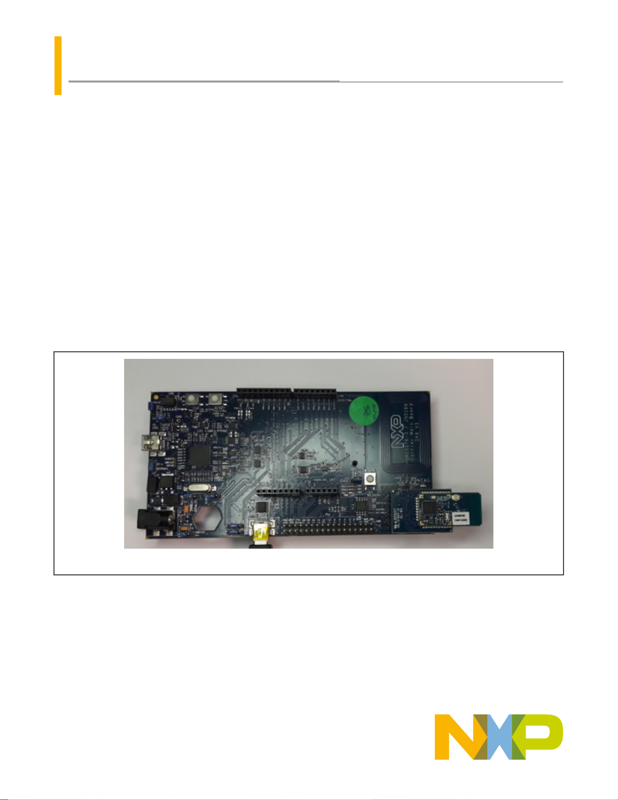
Figure 1. DK6 board with JN5189 module
2 Power consumption measurement
2.1 Test setup description
2.1.1 Hardware configuration
The test setup is composed of:
Page 2
NXP Semiconductors
Power consumption measurement
• One JN5189 module on a mezzanine board
• One modified DK6 board, as described in IoT-ZTB-DK006 Development Kit user guide UM11393
The test equipment chosen is a source/measure unit SMU (Keysight B2902A for instance). It is a power supply capable of
measuring low currents.
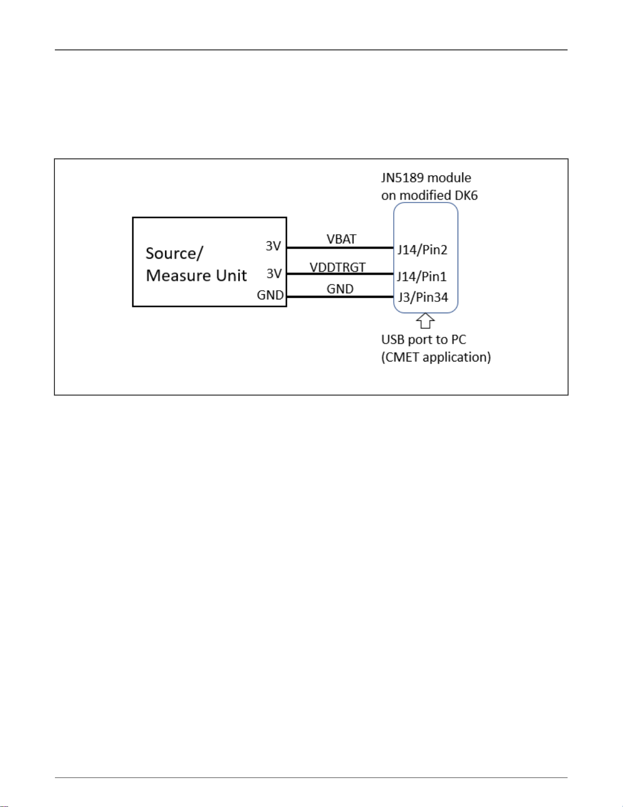
Test setup block diagram is shown in Figure 2.
Figure 2. Test setup block diagram for static measurements
The VBAT supplies the JN5189 device under the test while the VDDTRGT is used to supply the rest of the board. The purpose
is to measure the current on the JN5189 independently of the board consumption.
From a supply standpoint, VBAT = VDDTRGT.
The test connections are shown in Figure 3.
JN5189-Power Consumption Analysis, Rev. 1, 01/2021
Application Note 2 / 22
Page 3

NXP Semiconductors
Power consumption measurement
JN5189-Power Consumption Analysis, Rev. 1, 01/2021
Application Note 3 / 22
Page 4
NXP Semiconductors
Power consumption measurement
2.1.2 Software configuration
CMET is the software tool used for the power consumption measurement. It can be downloaded from the NXP website
(CMET/AN1242).
As described in
AN1242), the low-power modes are shown in Table 1.
Table 1. Power down currents description
Power mode CPU CPU clock RAM Wake-up source
PM_DEEP_DOWN OFF OFF OFF Hardware reset, I/O event
PM_DOWN OFF OFF Variable size Retention HW reset, I/O event, wake-up timer
PM_SLEEP ON OFF ON Any interrupt
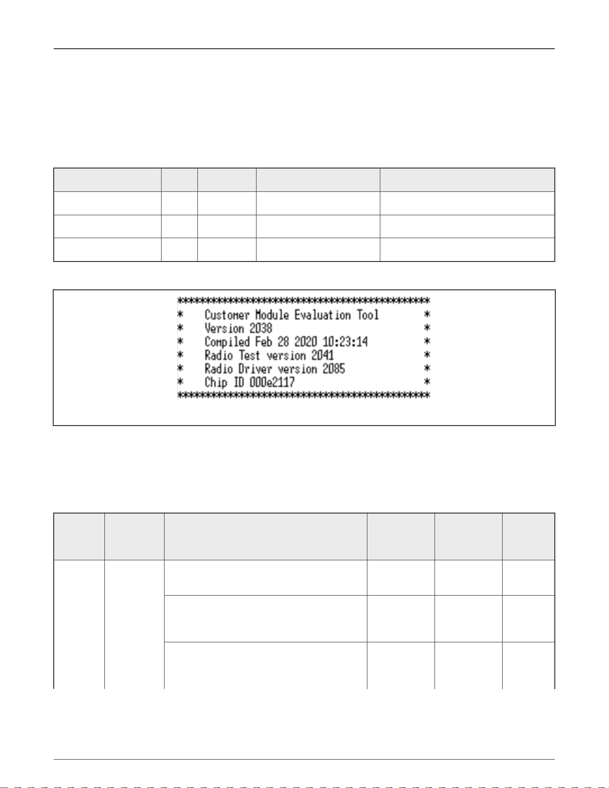
For this test, the CMET version used is shown in Figure 4.
Figure 4. CMET version
High Performance M68HC11 System Design Using The WSI PSD4XX and PSD5XX Families
(document
2.2 Power consumption in low-power modes
The power-down and deep power-down modes are covered by these measurements.
The currents measured with the CMET are shown in Table 2.
Table 2. CMET current measurements
Symbol Parameter Conditions
IDD Supply
current
Deep power-down (everything is powered off,
wakeup on hardware reset only)
Deep power-down-IO (everything is powered off,
wakeup on hardware reset only or an event on any
of the 22 GPIOs and the NTAG interrupt)
Power-down (wakeup on hardware reset or an
IO event, wake-up timer on, 32 kHz FRO on, no
SRAM retention)
Table continues on the next page...
(datasheet)
Type
250 235 nA
350 360 nA
800 880 nA
Measure with
CMET @VBAT
3 V
Units
JN5189-Power Consumption Analysis, Rev. 1, 01/2021
Application Note 4 / 22
Page 5
NXP Semiconductors
Table 2. CMET current measurements (continued)
Power profile measurement
Symbol Parameter Conditions
Power-down-4K (wakeup on hardware reset or an
IO event, wake-up timer on, 32 kHz FRO on, with
4 KB SRAM retention)
Power-down-8K (wakeup on hardware reset or an
IO event, wake-up timer on, 32 kHz FRO on, with
8 KB SRAM retention)
(datasheet)
2.3 Power consumption in the Active mode
The RF currents are measured with the CMET and the results are shown in Table 3.
Table 3. Active current results with CMET
Parameter Conditions
Supply
current
Radio in RX mode (IEEE 802.15.4) 4.30 6.84 mA
Radio in TX mode (IEEE 802.15.4),
output power 0 dBm
Requirement typical @Vbat 3 V
(CPU current not included)
7.36 10.15 mA
Type
1025 1085 nA
1120 1170 nA
CMET measurement @Vbat 3 V
(CPU current included)
Measure with
CMET @VBAT
3 V
Units
Units
Radio in TX mode (IEEE 802.15.4),
output power +3 dBm
Radio in TX mode (IEEE 802.15.4),
output power +10 dBm
The gap compared to the data sheet is due to the CPU current that is already a part of the CMET measurements.
9.44 12.21 mA
20.28 21.75 mA
NOTE
3 Power profile measurement
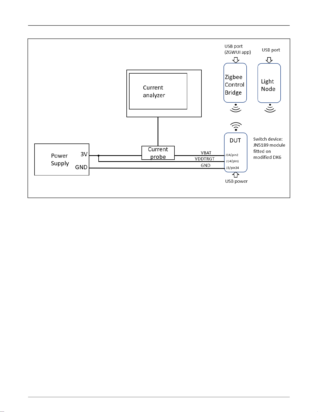
3.1 Hardware prerequisites
The setup is composed of the IOTZTB-DK006 kit content: a control bridge, a light node, and a switch device made of the JN5189
fitted on a DK6 board. Similarly to the previous chapters, the DK6 of the switch device is modified for power measurement.
The JN5189 fitted on a modified DK6 board is called “the switch device” further on in this document.
The block diagram of the test setup is shown in Figure 5.
JN5189-Power Consumption Analysis, Rev. 1, 01/2021
Application Note 5 / 22
Page 6
NXP Semiconductors
Power profile measurement
Figure 5. Test setup block diagram
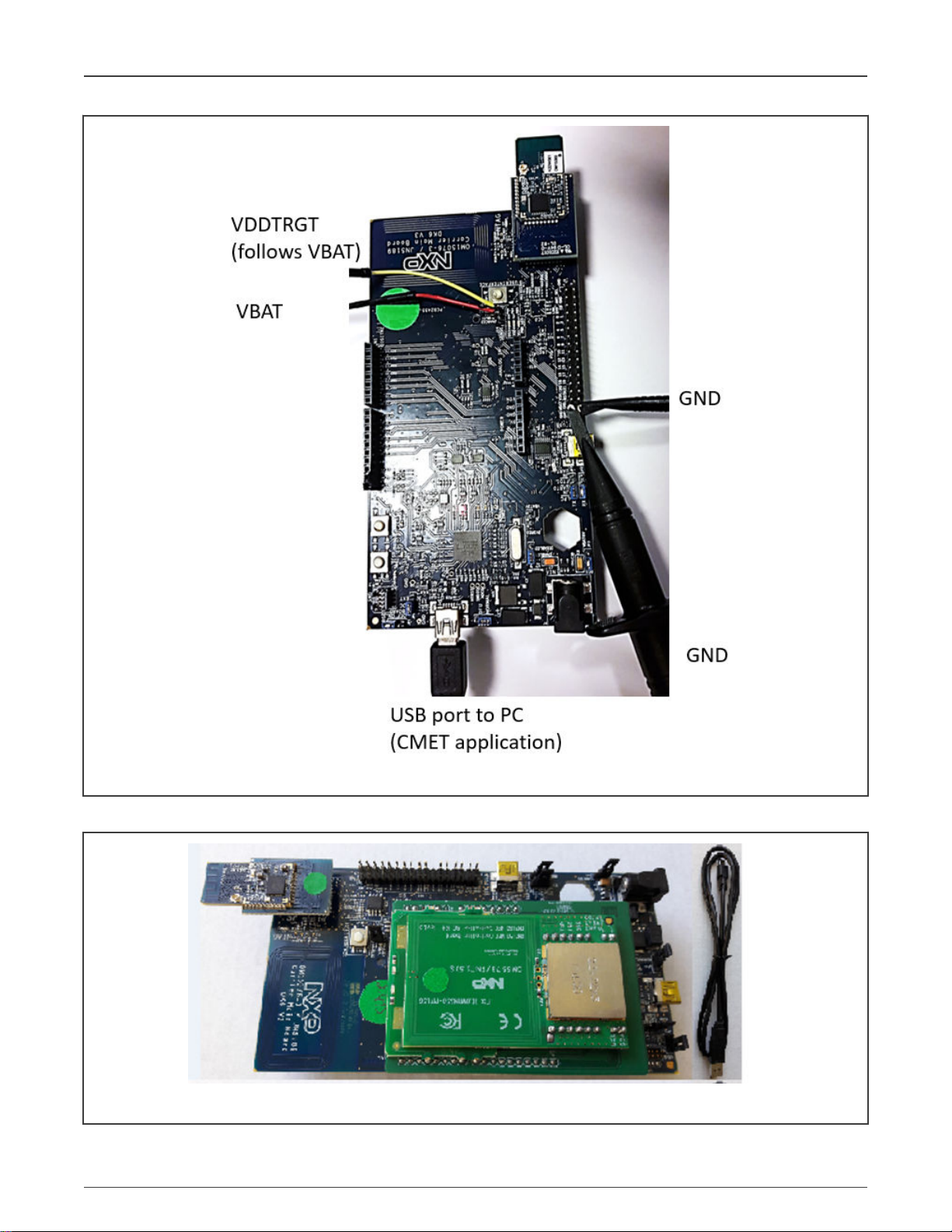
The modified DK6 with the JN5189 module fitted is shown in Figure 6.
JN5189-Power Consumption Analysis, Rev. 1, 01/2021
Application Note 6 / 22
Page 7
NXP Semiconductors
Power profile measurement
Figure 6. Modified DK6 and JN5189 module fitted
The Zigbee control bridge and the light node are shown in Figure 7 and Figure 8.
Figure 7. Zigbee control bridge
JN5189-Power Consumption Analysis, Rev. 1, 01/2021
Application Note 7 / 22
Page 8

NXP Semiconductors
The test setup is shown in Figure 9.
Figure 8. Light node
Power profile measurement
JN5189-Power Consumption Analysis, Rev. 1, 01/2021
Application Note 8 / 22
Page 9

NXP Semiconductors
Power profile measurement
Figure 9. Test setup
JN5189-Power Consumption Analysis, Rev. 1, 01/2021
Application Note 9 / 22
Page 10

NXP Semiconductors
Power profile measurement
3.2 Software configuration
A flash programmer is necessary to program the binary file into the flash memory of the device. The instructions are described in
the JN-SW-4407 application note, which is in the
The control bridge is configured using the instructions shown in document AN1247. The AN1223-Zigbee-IoT-Gateway-ControlBridge (ZGWUI) must be installed on the PC to connect the control bridge.
The light node is configured using the instructions in document AN1244.
The switch device is configured using the instructions in document JN-AN-1245. The switch used in this example has the following
parameters, which are described in document JN-AN-1245:
• DIO_TOGGLE=1
• DK6_TEST=1
The other settings for the next measurements are as follows:
• Payload: 37 B
• RAM size: 4 KB
• TX output power: 10 dBm
• Radio driver version: 2088
After the binary files are programmed into the device memory and before the procedure described in Measurement
procedure, all the devices must be unplugged from their USB ports or any external power supplies.
tools
folder of the SDK.
NOTE
NOTE
The DC-DC is always enabled in this measurement.
3.3 Use case description
A basic use case of a ZigBee network application is chosen as an example.
A light node joins a ZigBee network and it is controlled by a switch device via a control bridge. The control bridge is logging the
communication events thanks to the ZGWUI application on a PC.
3.4 Measurement procedure
3.4.1 Joining the network
The switch device must join the network to control the light node.
The ZGWUI application is used to start the network and it joins the devices.
The joining procedure is as follows:
1. Start the ZGWUI application on the PC.
2. In the "Settings" menu, select the COM port that corresponds to the control bridge, as shown in Figure 10 and Figure
11.
JN5189-Power Consumption Analysis, Rev. 1, 01/2021
Application Note 10 / 22
Page 11

NXP Semiconductors
Power profile measurement
Figure 10. ZigBee interface
JN5189-Power Consumption Analysis, Rev. 1, 01/2021
Application Note 11 / 22
Page 12

NXP Semiconductors
Power profile measurement
Figure 11. ZigBee settings
3. Select "Open port".
4. Erase the PD.
5. Set the channel in the CMSK field and select "Set CMSK". Type "15".
6. Start the NWK.
7. Connect the switch device to a USB port and to an external power supply (as shown in Hardware prerequisites).
8. Power on the external power supply.
9. In the ZGWUI, in the "Permit Join" field, type "0" into the first one and "20" into the second one. Select "Permit Join".
10. The switch device joins the network and can be verified in the log message on the ZGWUI, as shown in Figure 12.
JN5189-Power Consumption Analysis, Rev. 1, 01/2021
Application Note 12 / 22
Page 13

NXP Semiconductors
Power profile measurement
Figure 12. ZGWUI log message
11. Power on the light node by connecting it to a USB port.
Figure 13. Powering the light node
12. The light node flashes until it joins the network, as shown in Figure 13. Then the light is always ON.
JN5189-Power Consumption Analysis, Rev. 1, 01/2021
Application Note 13 / 22
Page 14

NXP Semiconductors
Power profile measurement
The power consumption can be observed when the switch device joins the network, as shown in Figure 14.
Figure 14. Joining power profile
The ZGWUI session must stay active for the next steps in the following chapters.
3.4.2 Binding the switch to the light node
When the switch device has joined the network, it is necessary to bind it to the light node. To do so, perform the following steps
in the same ZGWUI session as in the previous chapter:
1. On the light node, push the reset button (SW4 on DK6 board) three times:
JN5189-Power Consumption Analysis, Rev. 1, 01/2021
Application Note 14 / 22
Page 15

NXP Semiconductors
Power profile measurement
Figure 15. Light node: reset button location
1. The light node starts to flash.
2. On the switch device, press the user interface button (BP1) and release it. The light node LEDs stop flashing and stay
ON.
JN5189-Power Consumption Analysis, Rev. 1, 01/2021
Application Note 15 / 22
Page 16

NXP Semiconductors
Power profile measurement
Figure 16. Switch device: user interface button location
3. The switch device and the light node are bound and the switch device can control the light node according to Table 4.
Table 4. Light node rules
User interface button on the switch device Result on the light node
Push 2n+1, n = 0, 1, 2.. Light OFF
Push 2n, n = 0, 1, 2.. Light ON
The power profile is observed at the binding time (Figure 17).
JN5189-Power Consumption Analysis, Rev. 1, 01/2021
Application Note 16 / 22
Page 17

NXP Semiconductors
Power profile measurement
Figure 17. Binding power profile
The sniffing trace of a binding event is shown in Figure 18.
JN5189-Power Consumption Analysis, Rev. 1, 01/2021
Application Note 17 / 22
Page 18

NXP Semiconductors
Power profile measurement
Figure 18. Binding sniffer trace
3.4.3 Switching on the light node with the switch device
When the user pushes the user interface button of the switch device, the device goes through the following three phases:
1. Waking up from the sleep mode
2. Transmitting data
3. Going back to the sleep mode
In this case, the power profile can be measured as shown in Figure 19.
JN5189-Power Consumption Analysis, Rev. 1, 01/2021
Application Note 18 / 22
Page 19

NXP Semiconductors
Power profile measurement
Figure 19. Light-on event power profile
The shape of the current profile is the same when pushing the user interface button again to switch the light off.
The sniffer trace of a light-on event is as below:
Figure 20. Light-on event sniffer trace
The power profile is then processed as shown in Figure 21.
JN5189-Power Consumption Analysis, Rev. 1, 01/2021
Application Note 19 / 22
Page 20

NXP Semiconductors
Conclusion
Figure 21. Current profile of a ZigBee event
The power consumption is analyzed for several Vbat voltages, as shown in Table 5.
Table 5. Current measurements from a ZigBee profile
Step# CPU Radio Mode Current @ 2.6 V Current @ 3.0 V Current @ 3.6 V Duration
A Start OFF Initialization 2.5 mA 2.4 mA 2.4 mA 7.6 ms
B ON RX ON RX Cal- CCA 6.6 mA 6.5 mA 5.9 mA 172 µs
C ON TX ON 10 dBm 22.6 mA 19.8 mA 16.9 mA 1.7 ms
D ON RX ON Wait for Ack 6.7 mA 6.3 mA 5.7 mA 387 µs
E ON OFF PD Mode 0 2.70 µA 2.73 µA 2.85 µA NA
4 Conclusion
This application note provides a step by step approach to measure low-power performances of the JN5189. The measurements
are based on the Zigbee events that can be replicated using the development kit (IOTZTB-DK006).
The total energy consumed is in line with the specifications, which makes the JN5189 particularly suitable for lowpower applications.
JN5189-Power Consumption Analysis, Rev. 1, 01/2021
Application Note 20 / 22
Page 21

NXP Semiconductors
5 Revision history
Table 6. Revision history
Rev Date Description
1 01/2021 Typos corrected in Software configuration and Binding the switch to the light node.
0 09/2020 Initial version
Revision history
JN5189-Power Consumption Analysis, Rev. 1, 01/2021
Application Note 21 / 22
Page 22

How To Reach Us
Home Page:
nxp.com
Web Support:
nxp.com/support
Information in this document is provided solely to enable system and software implementers
to use NXP products. There are no express or implied copyright licenses granted hereunder
to design or fabricate any integrated circuits based on the information in this document. NXP
reserves the right to make changes without further notice to any products herein.
NXP makes no warranty, representation, or guarantee regarding the suitability of its products
for any particular purpose, nor does NXP assume any liability arising out of the application
or use of any product or circuit, and specifically disclaims any and all liability, including
without limitation consequential or incidental damages. “Typical” parameters that may be
provided in NXP data sheets and/or specifications can and do vary in different applications,
and actual performance may vary over time. All operating parameters, including “typicals,”
must be validated for each customer application by customer's technical experts. NXP does
not convey any license under its patent rights nor the rights of others. NXP sells products
pursuant to standard terms and conditions of sale, which can be found at the following address:
nxp.com/SalesTermsandConditions.
While NXP has implemented advanced security features, all products may be subject to
unidentified vulnerabilities. Customers are responsible for the design and operation of their
applications and products to reduce the effect of these vulnerabilities on customer’s applications
and products, and NXP accepts no liability for any vulnerability that is discovered. Customers
should implement appropriate design and operating safeguards to minimize the risks associated
with their applications and products.
NXP, the NXP logo, NXP SECURE CONNECTIONS FOR A SMARTER WORLD, COOLFLUX,
EMBRACE, GREENCHIP, HITAG, ICODE, JCOP, LIFE VIBES, MIFARE, MIFARE CLASSIC,
MIFARE DESFire, MIFARE PLUS, MIFARE FLEX, MANTIS, MIFARE ULTRALIGHT,
MIFARE4MOBILE, MIGLO, NTAG, ROADLINK, SMARTLX, SMARTMX, STARPLUG, TOPFET,
TRENCHMOS, UCODE, Freescale, the Freescale logo, AltiVec, CodeWarrior, ColdFire,
ColdFire+, the Energy Efficient Solutions logo, Kinetis, Layerscape, MagniV, mobileGT, PEG,
PowerQUICC, Processor Expert, QorIQ, QorIQ Qonverge, SafeAssure, the SafeAssure logo,
StarCore, Symphony, VortiQa, Vybrid, Airfast, BeeKit, BeeStack, CoreNet, Flexis, MXC, Platform
in a Package, QUICC Engine, Tower, TurboLink, EdgeScale, EdgeLock, eIQ, and Immersive3D
are trademarks of NXP B.V. All other product or service names are the property of their
respective owners. AMBA, Arm, Arm7, Arm7TDMI, Arm9, Arm11, Artisan, big.LITTLE, Cordio,
CoreLink, CoreSight, Cortex, DesignStart, DynamIQ, Jazelle, Keil, Mali, Mbed, Mbed Enabled,
NEON, POP, RealView, SecurCore, Socrates, Thumb, TrustZone, ULINK, ULINK2, ULINK-ME,
ULINK-PLUS, ULINKpro, µVision, Versatile are trademarks or registered trademarks of Arm
Limited (or its subsidiaries) in the US and/or elsewhere. The related technology may be protected
by any or all of patents, copyrights, designs and trade secrets. All rights reserved. Oracle
and Java are registered trademarks of Oracle and/or its affiliates. The Power Architecture and
Power.org word marks and the Power and Power.org logos and related marks are trademarks
and service marks licensed by Power.org.
©
NXP B.V. 2021. All rights reserved.
For more information, please visit: http://www.nxp.com
For sales office addresses, please send an email to: salesaddresses@nxp.com
Date of release: 01/2021
Document identifier: AN12898
 Loading...