

Page 1
AN12550
PNEV5190B evaluation board quick start guide
Rev. 1.5 — 23 April 2021 Application note
562315 COMPANY PUBLIC
Document information
Information Content
Keywords PN5190, PNEV5190B, PNEV5190M, PN5190 evaluation board, PN5190
customer board, PN5190 GUI, GUI, PN5190 support tool, NFC Cockpit
Abstract This document describes the PNEV5190B V1.0 (PN5190 evaluation board),
and how to use it. It describes the NFC Cockpit (PN5190 GUI Version 5.5.0
or later), which allows an easy basic access to the PN5190 registers and
EEPROM in combination with basic reader functionality.
Page 2
NXP Semiconductors
1 Revision history
Revision history
Rev Date Description
1.5 20210423
1.4 20201218
1.3 20200929
1.2 20200109
1.1 20191217
1.0 20191128
• The format of this application note has been redesigned to comply with the new identity
guidelines of NXP Semiconductors.
• Section 6: updated
Update of the software section
Update versions numbers for PN5190 CQS1
Figure 6 layout corrected
AN number corrected, typos removed
First version
AN12550
PNEV5190B evaluation board quick start guide
AN12550 All information provided in this document is subject to legal disclaimers. © NXP B.V. 2021. All rights reserved.
Application note Rev. 1.5 — 23 April 2021
COMPANY PUBLIC 562315 2 / 37
Page 3

NXP Semiconductors
2 Introduction
This document describes the PNEV5190B (PN5190 evaluation board), which provides an
easy evaluation of the features and functions of the PN5190.
It provides the first steps to operate the board, using the NFC Cockpit (PN5190 GUI
Version 5.5.0 or higher).
The default antenna is a 45 mm x 45 mm antenna with some metal layer inside
the antenna area. This antenna is not an optimum antenna as such, but intends to
demonstrate the performance and register settings of the PN5190 under typical design
constraints like LCD or some metal (e.g. PCB) inside the antenna area. The default
settings provide an EMVC0 3.0 L1 analog compliance under the assumption that the
antenna surface is a few mm above the antenna PCP.
2.1 PN5190 registers and EEPROM concept
The PN5190 uses internal registers to adapt and optimize the functionality and
performance for each of the supported protocols and data rates dependent on the
connected antenna, matching network and receiver path. It offers an EEPROM, which
contains the default settings for all the supported protocols. These settings are loaded
into the registers with the LOAD_RF_CONFIGURATION (0Dh) command for each
supported protocol and data rate.
AN12550
PNEV5190B evaluation board quick start guide
The default EEPROM configuration settings are optimized for the 45 mm x 45 mm
antenna of the board PNEV5190B and can be changed by the user in case a customized
antenna and matching network is used. The command LOAD_RF_CONFIGURATION
allows initializing multiple registers with an efficient single command and allows
distinguishing between transmit and receive configuration. Update of the registers
relevant for a selected protocol is done by copying the content of EEPROM addresses
to registers. Not all protocols require the initialization of all or the same registers, the
command LOAD_RF_ CONFIGURATION considers this by initializing the registers
relevant for the currently selected protocol only.
The EEPROM content can be updated using the command
UPDATE_RF_CONFIGURATION (0Eh). The command does not require any physical
EEPROM address, but works directly with the register address information and the
protocol for which this data is intended to be used. This allows a convenient initialization
of all relevant values for operation.
Some of these settings can or even must be adapted toward a new antenna design (e.g.
the dynamic power control). All those design-specific settings should be stored in the
PN5190 EEPROM to allow a proper functionality.
Some EEPROM configuration data is independent from the used protocols and defines
e.g. the startup behavior of the PN5190 or the functionality of low-power card detection
(LPCD). This configuration data might also be adapted for optimum performance of the
chip.
2.2 PNEV5190B concept
The basic concept of the PNEV5190B is to enable the user to perform a quick
evaluation of the PN5190 and also connect their own antenna to the PNEV5190B
board. In addition, dedicated boards which allow to solder custom antenna matching
components are available. The NFC Cockpit can be used to optimize the RF
AN12550 All information provided in this document is subject to legal disclaimers. © NXP B.V. 2021. All rights reserved.
Application note Rev. 1.5 — 23 April 2021
COMPANY PUBLIC 562315 3 / 37
Page 4

NXP Semiconductors
performance of the PN5190 antenna tuning, to perform the DPC calibration and the
related TX and RX optimization without touching any source code.
All the relevant registers can be modified and fine-tuned using the NFC Cockpit. After
successful register optimization, the found settings can be stored in the PN5190
EEPROM.
The NFC Cockpit also allows a dump of the complete user EEPROM content into an
XML file. This file then can be loaded again into the EEPROM. That allows to manage
and exchange different user or antenna configurations. In addition, the optimized register
settings using the NFC Cockpit can be used during user code development as well.
As soon as the register settings for the targeted protocols and data rates are defined, the
NFC Reader Library including the HAL can be used to start the development of the user
application. Examples illustrate the usage of the library for typical use cases.
The source code examples of the NFC Reader Library can be used to develop an own
application directly on the Kinetis MCU K82 (see [4]) or can serve as a starting point for
porting the NXP NFC Reader Library to any other microcontroller platform.
AN12550
PNEV5190B evaluation board quick start guide
AN12550 All information provided in this document is subject to legal disclaimers. © NXP B.V. 2021. All rights reserved.
Application note Rev. 1.5 — 23 April 2021
COMPANY PUBLIC 562315 4 / 37
Page 5

NXP Semiconductors
3 Hardware
The PNEV5190B V1.0, as shown in Figure 1, provides some test functions which might
not be used for the typical hardware and software evaluation. The PNEV5190M (module)
can be used as a simple standard reader module without modification. In addition, it can
be used to define and optimize the analog settings for any connected antenna or it can
be used to develop and modify any RFID and NFC application based on the NFC Reader
Library.
3.1 Hardware introduction
The PN5190 is supplied with a supply voltage, which can be chosen between internal
and external supply. For the internal supply either 5 V, 3.3 V or 1.8 V (for VDDIO) can
be used. The external power supply must be between 5 V and 12 V DC (polarity does
not matter) since the board provides a rectifier and LDO to supply the circuit with 6 V
(optional, supply voltage ≥7.5 V), 5 V, 3.3 V and 1.8 V.
Warning: The PN5190 in default configuration requires an external power supply, i.e. the
USB supply does not provide enough current.
AN12550
PNEV5190B evaluation board quick start guide
The PN5190 is connected to a Kinetis K82 121BGA µC via SPI. A specific firmware on
the K82 allows using the PNEV5190B together with the NFC Cockpit.
The connection to the PC is done via USB micro connection.
Another connection option allows connecting a Linker / LPC-LINK2 board to the
PNEV5190B with a debug cable. This allows the development of custom software or the
execution of the NXP NFC Reader Library code including samples.
In case a different host microcontroller shall be used, the SPI interface is available for
connection to an external host (the onboard K82 is not used in this case).
AN12550 All information provided in this document is subject to legal disclaimers. © NXP B.V. 2021. All rights reserved.
Application note Rev. 1.5 — 23 April 2021
COMPANY PUBLIC 562315 5 / 37
Page 6
NXP Semiconductors
AN12550
PNEV5190B evaluation board quick start guide
1. Version 1.0
Figure 1. PNEV5190B Customer evaluation board
The PNEV5190B customer evaluation board consists of 2 PCBs:
The PNEV5190B (base board) and the PNEV5190M (module board), as shown in
Figure 2 and Figure 3. The PNEV5190M is soldered onto the PNEV5190B and contains
the PN5190 itself and the major components, as required to operate the IC, e.g. the DCDC inductor, the EMC filter and some block capacitors. The layout of the module board
can be taken as reference.
AN12550 All information provided in this document is subject to legal disclaimers. © NXP B.V. 2021. All rights reserved.
Application note Rev. 1.5 — 23 April 2021
COMPANY PUBLIC 562315 6 / 37
Page 7
NXP Semiconductors
Figure 2. PNEV5190B base board top view (placement)
AN12550
PNEV5190B evaluation board quick start guide
Figure 3. PNEV5190M Module board top view (placement)
3.2 Schematics
The complete schematics of the PNEV5190B base board are shown in the following
figures. The more detailed reference data is available in [5].
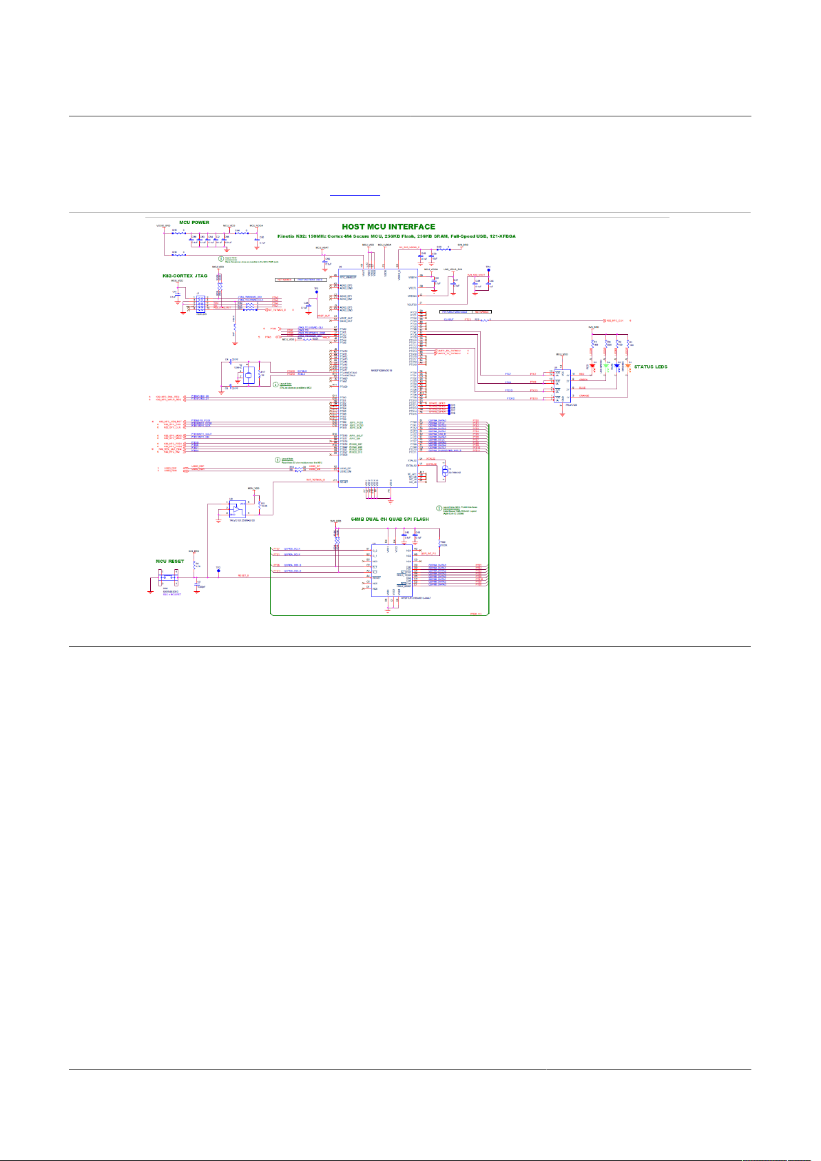
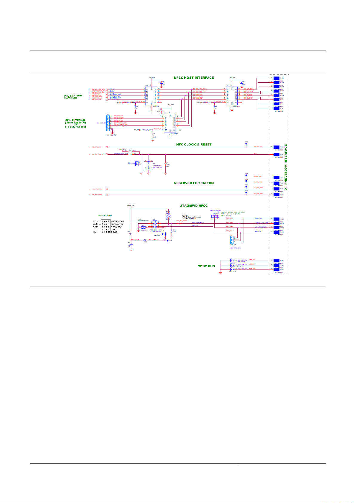
3.2.1 K82
The PNEV5190B uses a Kinetis K82 121BGA microcontroller (Figure 4).
An LPC Link can be connected to the K82 via the JTAG/SWD interface (see Figure 5).
AN12550 All information provided in this document is subject to legal disclaimers. © NXP B.V. 2021. All rights reserved.
Application note Rev. 1.5 — 23 April 2021
COMPANY PUBLIC 562315 7 / 37
Page 8
NXP Semiconductors
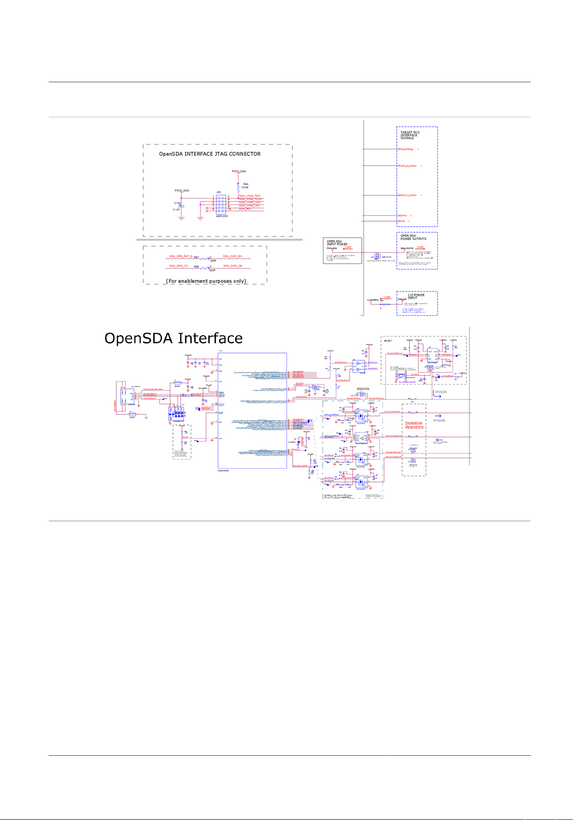
In addition, an OpenSDA interface is provided for debugging the K82 by using a Kinetis
MK20DX128VFM5 (Figure 6).
AN12550
PNEV5190B evaluation board quick start guide
Figure 4. K82 main schematics
AN12550 All information provided in this document is subject to legal disclaimers. © NXP B.V. 2021. All rights reserved.
Application note Rev. 1.5 — 23 April 2021
COMPANY PUBLIC 562315 8 / 37
Page 9
NXP Semiconductors
AN12550
PNEV5190B evaluation board quick start guide
Figure 5. PNEV5190M interface
AN12550 All information provided in this document is subject to legal disclaimers. © NXP B.V. 2021. All rights reserved.
Application note Rev. 1.5 — 23 April 2021
COMPANY PUBLIC 562315 9 / 37
Page 10
NXP Semiconductors
AN12550
PNEV5190B evaluation board quick start guide
Figure 6. OpenSDA for K82 (MK20DX128VFM5)
3.2.2 Power supply
The default settings use the external power supply from the power jack connector. The
external power supply must always be used, if the DC-DC is enabled (default). The DC
power input can cover a DC voltage around 7.5 V with a current of at least 800 mA. The
polarity does not matter, since there is a rectifier foreseen. The inrush current of the DCDC can be up to 1.6 A, when enabling the RF field.
AN12550 All information provided in this document is subject to legal disclaimers. © NXP B.V. 2021. All rights reserved.
Application note Rev. 1.5 — 23 April 2021
COMPANY PUBLIC 562315 10 / 37
Page 11
NXP Semiconductors
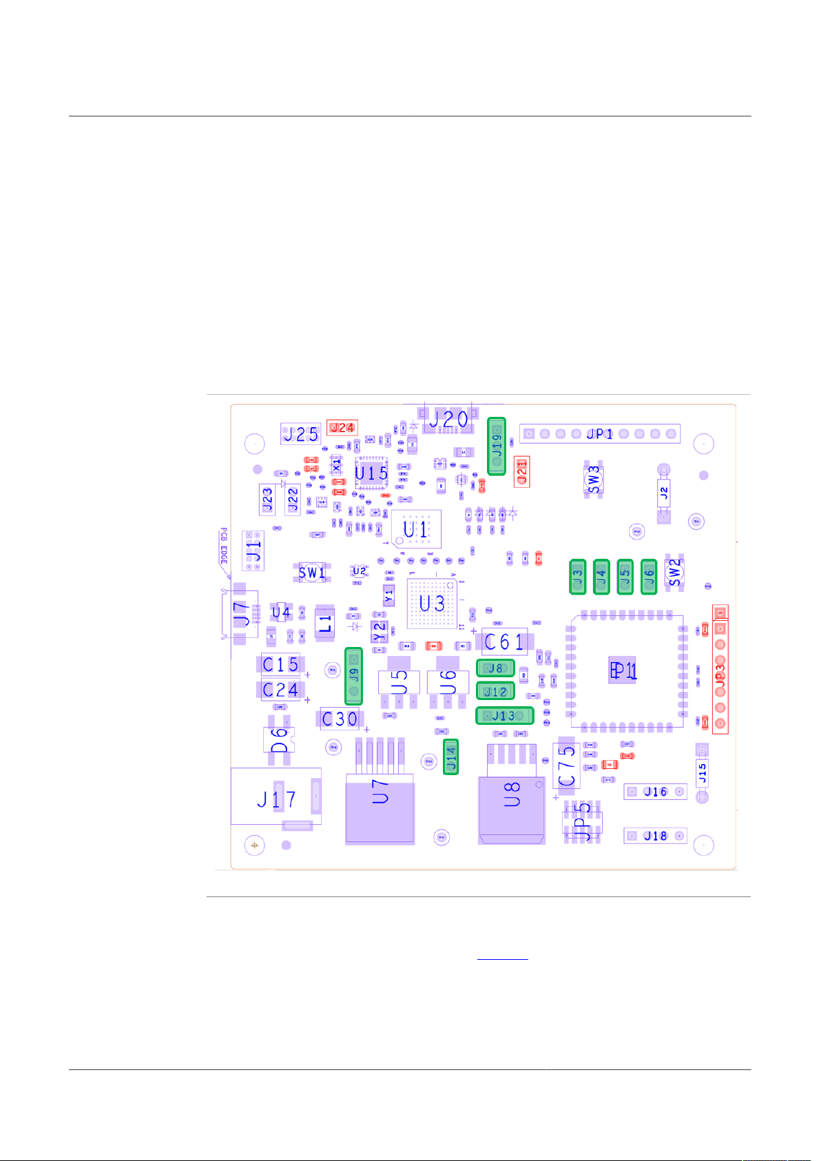
Figure 7. Figure title here
AN12550
PNEV5190B evaluation board quick start guide
As soon as the board is supplied with power, the red LED D5 must be on.
The PNEV5190B has different supply pins for the PNEV5190M (module board) as shown
in Table 1. For further details on the supply options of the PN5190 itself, refer to [1].
Table 1. PNEV5190M module supply pins
Attention: there are PN5190 (IC) pins with the same name!
Pin Name Type Description
VBAT Supply input 3.3 V Main Input Supply Voltage
VBATPWR Supply input = VBAT = 3.3 V Main Input Supply Voltage
VDDIO Supply input 1.8 V IO power supply
VUP - not used in default configuration
The PN5190B base board provides four LDOs:
1. U8 for supplying the PNEV5190M with VBAT. The default configuration provides
VBAT = 3.3 V. Optionally this voltage can be set to 4.8 V.
2. U5 for supplying the VDDIO and the µC supply (VDDIO_BRD = MCU_VDD =
MCU_VDDA) with 3.3 V. This LDO is not used in default configuration.
3. U6 for supplying the VDDIO and the µC supply (VDDIO_BRD = MCU_VDD =
MCU_VDDA) with 1.8 V. This LDO is used in default configuration.
4. U7 for supplying the overall board with 6 V. This LDO is used in default configuration.
The default configuration uses the following jumpers closed:
J9: 2-3 -> external power supply
J8: closed -> VBATPWR supplied with VBAT = 3.3 V
J12: closed -> VBAT supplied with 3.3 V
The default configuration uses the following jumpers open:
J3: open
AN12550 All information provided in this document is subject to legal disclaimers. © NXP B.V. 2021. All rights reserved.
Application note Rev. 1.5 — 23 April 2021
COMPANY PUBLIC 562315 11 / 37
Page 12
NXP Semiconductors
J4: open
J5: open
J6: open
J13: open (this jumper can be used to bypass the DC-DC, but only if the EEPROM
settings are done properly AND the required board modifications are made properly)
J14: open
J8 can be used to measure the current consumption of the TX driver circuit including the
DC-DC.
J12 can be used to measure the supply current consumption, excluding the TX driver
part.
AN12550
PNEV5190B evaluation board quick start guide
Figure 8. PBEV5190B jumpers
3.2.3 PNEV5190M module board
The PNEV5190M module board is shown in Figure 9. The module board contains
the most relevant components, directly connected to the PN5190, i.e. the EMC filter
inductors, the DC-DC inductor, the major block capacitors and the 27.12 MHz crystal.
The default clock is based on this 27.12 MHz crystal, but the board supports the option to
test external clock input, if needed.
AN12550 All information provided in this document is subject to legal disclaimers. © NXP B.V. 2021. All rights reserved.
Application note Rev. 1.5 — 23 April 2021
COMPANY PUBLIC 562315 12 / 37
Page 13

NXP Semiconductors
The relevant test signals can be derived from the test pins at the bottom of the board.
AN12550
PNEV5190B evaluation board quick start guide
1. GND pads: 8,11,13,16,37
2. RFU pads: 7, 30, 31
Figure 9. PNEV5190M module board schematics
3.2.4 PNEV5190 antenna
The antenna connection uses the standard tuning circuit. The EMC filter is designed with
a cut-off frequency of f
16Ω.
The details of antenna tuning are described in [2].
EMC
= 14.25 MHz, and the antenna impedance is tuned to Z = 15…
AN12550 All information provided in this document is subject to legal disclaimers. © NXP B.V. 2021. All rights reserved.
Application note Rev. 1.5 — 23 April 2021
COMPANY PUBLIC 562315 13 / 37
Page 14

NXP Semiconductors
1. 45 mm x 45 mm antenna coil connected to J10
Figure 10. PNEV5190B antenna circuit
AN12550
PNEV5190B evaluation board quick start guide
The PN5190 antenna tuning (see Figure 11) improves the transfer function compared to
the standard “asymmetrical” tuning and therefore allows using a higher system Q factor,
which results in a higher field strength. The disadvantage of the loading effect, which
causes an increased current ITVDD, is compensated with the PN5190 Dynamic Power
Control (DPC, for details refer to [3]). For more details on the PN5190 antenna tuning,
refer to [2] PN5190 Antenna design guide.
Figure 11. PNEV5190B evaluation board antenna tuning
AN12550 All information provided in this document is subject to legal disclaimers. © NXP B.V. 2021. All rights reserved.
Application note Rev. 1.5 — 23 April 2021
COMPANY PUBLIC 562315 14 / 37
Page 15

NXP Semiconductors
3.3 K20 OpenSDA interface
Software for K20 will come in future:
To use the OpenSDA debug for the K82, JP24 needs to be closed (default open)
Figure 12. PNEV5190 customer evaluation board jumper
3.4 LED status indication
AN12550
PNEV5190B evaluation board quick start guide
There is a power red LED, indicating the board is properly powered. It is driven by the
3V3 output of U6.
There are four LEDs (D1…D4) available, indicating some function of the PNEV5190B:
1. When RESET button is released, the LEDs flash to indicate that the secondary K82
FW and the PN5190 FW is working properly.
2. The blue LED indicates, that no VCOM interface is opened.
3. The green LED turns on, when the VCOM interface is opened.
4. The orange LED indicates a communication via SPI.
3.5 Jumper settings
The default jumper settings allow a direct use with the USB connector and an external
power supply. This might show limited performance due to a current limitation on the USB
host. So for real performance measurements, the external power supply should be used.
3.5.1 USB only
USB only (no external power supply) is not recommended at all. Most USB Hosts cannot
supply sufficient power over all nor handle an inrush current of 1.6 A.
3.5.2 External power supply
The default configuration requires an external 5 V DC power supply, providing at least
800 mA (up to 1.6 A inrush).
3.5.3 First-time use
Make sure that the K82 is flashed with the correct firmware NNC_uC_VCOM_03.05.09
(Compiled on Sep 24 2020 13:37:14) or later.
AN12550 All information provided in this document is subject to legal disclaimers. © NXP B.V. 2021. All rights reserved.
Application note Rev. 1.5 — 23 April 2021
COMPANY PUBLIC 562315 15 / 37
Page 16

NXP Semiconductors
4 PN5190 secure firmware update
The PN5190 supports secure firmware update and it provides an easy way to upload
the firmware via the NFC Cockpit tool or by an application hosted on the microcontroller,
which implements secure firmware update functionality.
This document describes the process of how to flash the PN5190 FW to the PNEV5190B
evaluation board. It also explains how to prepare the firmware update software for any
microcontroller connected to the PN5190 IC.
The PNEV5190B customer evaluation board and MCUXpresso IDE toolchain are used
as a reference to describe the functionality.
4.1 Requirements
This section describes the system and hardware requirements needed to upload the new
version of the PN5190 FW.
4.1.1 System requirements
AN12550
PNEV5190B evaluation board quick start guide
NFC Cockpit tool requirements:
• The chapters below are describing the installation process of it
• PC with USB port running on Microsoft Windows 10 operating system
• VCOM CDC drivers (drivers are available in the installation package)
Firmware download library requirements:
• Secure FW upload demo application is available in the provided release package
• The demo application is prepared for the MCUXpresso IDE toolchain.
4.1.2 Hardware requirements
• Enabled SPI host connection between microcontroller and PN5190 IC
• USB connection between PC and microcontroller
Note:
PNEV5190B evaluation board provides all features required to test “Secure FW update”.
4.2 Block diagram overview
At a very high level, the system is divided into three parts.
• PC host
• Microcontroller host
• PN5190
AN12550 All information provided in this document is subject to legal disclaimers. © NXP B.V. 2021. All rights reserved.
Application note Rev. 1.5 — 23 April 2021
COMPANY PUBLIC 562315 16 / 37
Page 17

NXP Semiconductors
Figure 13. PNEV5190 firmware block diagram
AN12550
PNEV5190B evaluation board quick start guide
4.2.1 PC host
The PC is hosting the NFC Cockpit tool, and it should provide a USB connection. The PC
host is connected to the microcontroller host via a USB Serial VCOM interface.
PC host is optional; it is required in case of using the NFC Cockpit tool.
4.2.2 Microcontroller host
Microcontroller, in this setup, works as a medium between PC and PN5190. The purpose
of it is to receive data from the PC over the USB interface and forward them to PN5190
via the SPI interface.
In case of setup, where secure FW update application is hosted on the microcontroller
host, the app reads the firmware data from an external source and sends them to
PN5190 IC via SPI interface.
4.2.3 PN5190
The PN5190 is a highly integrated high-performance full NFC Forum-compliant frontend
IC for contactless communication at 13.56 MHz.
PN5190 supports secure FW updates, and guidelines are described in the next sections.
4.3 Reference application
NXP provides “DownloadLibEx1” application as a reference example, which
demonstrates how to flash a new firmware by an application hosted on the target
microcontroller. The example includes the implementation of all needed commands in the
“Secure firmware download” mode.
The reference application package is prepared for the Kinetis K82 µC, and it works
together with the PNEV5190B development board. The project is built with the
MCUXpresso IDE.
AN12550 All information provided in this document is subject to legal disclaimers. © NXP B.V. 2021. All rights reserved.
Application note Rev. 1.5 — 23 April 2021
COMPANY PUBLIC 562315 17 / 37
Page 18

NXP Semiconductors
A reference example uses secure download library, which provides the implementation of
the secure download APIs. It is recommended to use it in the customer application.
4.3.1 Preconditions
It is required to set up the system comprising the PNEV5190B evaluation board and
LPC-Link2 or Segger J-Link, as shown in the figure below.
To be able to use the prepared software package, all components listed in the table
below are required:
Table 2. Development Environment
Device Version Description
PNEV5190B 1.0 or higher PNEV5190 Customer evaluation board (hardware)
LPC-LINK2 1.0 Standalone debug adapter (hardware)
MCUXpresso IDE 11.2.0 or higher Development IDE (PC software)
The next figure shows how to connect the PNEV5190B Development board with Segger
J-Link and PC. The development board in this setup is powered by USB (which is not
recommended if the RF Front-End is used).
AN12550
PNEV5190B evaluation board quick start guide
Figure 14. System setup
Before continuing, it is necessary to download the latest PN5190 SW release package
and extract it to an empty folder.
4.3.2 Import reference project
To import secure firmware update project, follow steps below:
1. Open MCUXpresso IDE in a new workspace
2. Import project from the previously extracted folder
AN12550 All information provided in this document is subject to legal disclaimers. © NXP B.V. 2021. All rights reserved.
Application note Rev. 1.5 — 23 April 2021
COMPANY PUBLIC 562315 18 / 37
Page 19

NXP Semiconductors
AN12550
PNEV5190B evaluation board quick start guide
1. Click “Import projects …” in the Project Explorer window
2. Select “General/Existing Projects into Workspace” option and click “Next” button
3. Browse to the “Secure_Fw_Downloader” folder
4. Select projects as shown on the picture above and click the “Finish” button
Figure 15. Import Secure Firmware Project to the MCUXpresso IDE
4.3.3 Build, run and debug project
After a successful project import, check for the correct project configuration. All three
projects shall be configured for “DebugFRDMK82F”.
AN12550 All information provided in this document is subject to legal disclaimers. © NXP B.V. 2021. All rights reserved.
Application note Rev. 1.5 — 23 April 2021
COMPANY PUBLIC 562315 19 / 37
Page 20

NXP Semiconductors
AN12550
PNEV5190B evaluation board quick start guide
1. Right-click on the project
2. Select “Build Configurations/SetActive/DebugFRDMK82F” option
Figure 16. Import secure firmware project to the MCUXpresso IDE
After that step, the project structure shall look like in the picture below.
Figure 17. Project Explorer Window
As a next step, it is necessary to build all projects. That can be achieved by clicking the
“Build all projects” in the “Quickstart Panel”.
The next step is to flash and debug the application. Highlight the “DownloadLibEx1”
project in the “Project Explorer” window and click “Debug” in the “Quickstart Panel”,
as shown in the next figure. The MCUXpresso IDE builds the application, flash the
application binary, and starts with the debugging process.
AN12550 All information provided in this document is subject to legal disclaimers. © NXP B.V. 2021. All rights reserved.
Application note Rev. 1.5 — 23 April 2021
COMPANY PUBLIC 562315 20 / 37
Page 21

NXP Semiconductors
AN12550
PNEV5190B evaluation board quick start guide
Figure 18. Flash and debug application
After that, the application starts, and it printout options for the supported tasks.
Figure 19. Application debug printouts
4.3.4 Secure download library
“Secure download library” is part of the reference application and provides an
implementation of the secure download mode. The secure download library is written in
C programing language, and it can be ported to any customer application running on the
µC.
Secure download library contains an implementation of the platform (SPI interface and
HW configuration), and this part of the library should be adopted in case it is used on any
other platform.
It is highly recommended to use the secure download library in the customer application.
The table below lists all APIs supported by the library:
AN12550 All information provided in this document is subject to legal disclaimers. © NXP B.V. 2021. All rights reserved.
Application note Rev. 1.5 — 23 April 2021
COMPANY PUBLIC 562315 21 / 37
Page 22

NXP Semiconductors
Table 3. API provided by secure download library
Device Description
phDlhalHw_Pn5190_Download_Init Initialize the download library.
phDlhalHw_Pn5190_Download_CheckIntegrity Returns the integrity information of the
phDlhalHw_Pn5190_Download_
CheckSessionState
AN12550
PNEV5190B evaluation board quick start guide
existing firmware.
Check and return the current download
session state.
AN12550 All information provided in this document is subject to legal disclaimers. © NXP B.V. 2021. All rights reserved.
Application note Rev. 1.5 — 23 April 2021
COMPANY PUBLIC 562315 22 / 37
Page 23

NXP Semiconductors
5 Software
The PNEV5190B evaluation board is delivered with a graphical user interface application
(GUI), the NXP NFC Cockpit. The NFC Cockpit can be used to explore the functionality
of the PN5190 and perform RF and antenna design-related tests. It allows a direct
register access as well as EEPROM read and writes access, and it allows testing and
calibrating the DPC. The NFC Cockpit therefore, can be used to configure and test the
PN5190.
5.1 K82 firmware and driver
The K82 firmware is installed by default on the PNEV5190B and is ready to use. So, no
Kinetis firmware installation is required, if the board is only used with the NFC Cockpit.
However, the K82 might be used for software development together with one of the
samples (including the NXP NFC Reader Library). In this case, the K82 FW must be
reinstalled afterwards, if the PNEV5190B is supposed to be used together with the NFC
Cockpit again. Reason for this is that any software development using the MCUXpresso
will erase the default firmware. Therefore, the K82 FW installation is described in the
following section.
AN12550
PNEV5190B evaluation board quick start guide
In any case, the correct PC driver must be installed, before the NFC Cockpit can be used
with the PNEV5190B evaluation board.
5.2 PN5190 NFC Cockpit
The PN5190 NFC Cockpit can be installed and started (see Figure 20).
1. Status when starting the NFC Cockpit with connected PNEV5190B board
Figure 20. NFC Cockpit with PNEV5190B initial view
After starting the NFC Cockpit, the communication link between the PC and the
PNEV5190B (via the K82 interface) is enabled automatically.
Note:
AN12550 All information provided in this document is subject to legal disclaimers. © NXP B.V. 2021. All rights reserved.
Application note Rev. 1.5 — 23 April 2021
COMPANY PUBLIC 562315 23 / 37
Page 24

NXP Semiconductors
The PN5190 NFC Cockpit is a development tool, and therefore allows many different
kinds of operations, even “useless” ones at a first glance. The correct use of the NFC
Cockpit is required to operate the PN5190 properly.
Example: Without enabling the field, no card can be operated, even though the PN5190
can be operated.
Figure 21 shows the activation of a MIFARE DESFire card, using the <Load Protocol>
+ <Field On> + <Activate Layer3>, followed by <Activate Layer4>. The PN5190 NFC
Cockpit shows the card responses like ATQA, SAK, and ATS.
Afterwards the ISO/IEC 14443-4 protocol can be used to exchange data. Figure 21
shows the MIFARE DESFire command “Get Application ID” (0x6A), which returns the
AIDs.
Note:
Make sure that either the CRC is enabled or added manually in the data field.
AN12550
PNEV5190B evaluation board quick start guide
1. 0x6a = Get Application ID command of MIFARE DESFire EV1
Figure 21. PN5190 NFC Cockpit: Activation of a MIFARE DESFire EV1 card + Get
Application ID
Similar functionality does exist for ISO/IEC 14443 A and B, for NFC type F and for ISO/
IEC 15693 communication.
Be aware that a LOAD_RF_CONFIG command must be executed manually before the
corresponding protocol settings are loaded from the EEPROM into the registers. This can
be used to perform:
1. <Load Protocol> (e.g. type A 106)
2. <Field On>
3. <Single REQA> (using the EEPROM settings)
4. Select a TX register, e.g. RF_CONTROL_TX, enable
TX_SET_BYPASS_SC_SHAPING
5. Change some register bits, and write back into RAM
6. <Single REQA> shows the register changes (probing the field and checking the
envelope)
AN12550 All information provided in this document is subject to legal disclaimers. © NXP B.V. 2021. All rights reserved.
Application note Rev. 1.5 — 23 April 2021
COMPANY PUBLIC 562315 24 / 37
Page 25

NXP Semiconductors
This allows an easy and quick optimization of TX and RX parameters before changing
the EERPOM.
1. <Load Protocol> (e.g. type A 106)
2. <Single REQA> (using again the EEPROM settings)
5.2.1 PN5190 register access
The PN5190 NFC Cockpit allows the reading and writing of all the PN5190 registers (see
Figure 22).
Selecting a register reads and shows the hexadecimal content as well as the
corresponding bit values. The input allows changing each bit separately as well as writing
hexadecimal values. Writing back the value changes the PN5190 register.
A help function automatically shows a short description of the (part of the) registers itself,
if the mouse is moved over the names.
Note:
Some register content cannot be changed manually (“read only”) and some content might
be overwritten by the PN5190 firmware.
AN12550
PNEV5190B evaluation board quick start guide
1. Register area is a RAM area, i.e. might be overwritten or changed automatically.
Figure 22. PN5190 register access
All registers, which are used in the LOAD_RF_CONFIG command, can be read from the
EEPROM. The user must select the register and the protocol.
All registers, which are used in the LOAD_RF_CONFIG command, can be written into
the EEPROM. The user must select the register and the protocol.
This allows an easy EEPROM update of the relevant TX and RX registers after
optimization in RAM.
5.2.2 PN5190 direct EEPROM access
The NFC Cockpit allows 4 options of EEPROM access (see Figure 23):
AN12550 All information provided in this document is subject to legal disclaimers. © NXP B.V. 2021. All rights reserved.
Application note Rev. 1.5 — 23 April 2021
COMPANY PUBLIC 562315 25 / 37
Page 26

NXP Semiconductors
• Read EEPROM
Reads a single byte from EEPROM using byte address
• Write EEPROM
Writes a single byte into EEPROM using byte address
• Dump EEPROM
Stores the complete user area of the PN5190 EEPROM into an XML file. This can be
used to generate a backup of all settings or to transfer optimized settings onto another
board or into own software. It makes sense to save all default EEPROM settings into a
file, before modifying the EEPROM.
• Load EEPROM
Loads an XML file and stores the content into the user area of the PN5190 EEPROM.
The format is fixed and must fit.
AN12550
PNEV5190B evaluation board quick start guide
1. EEPROM means User area of the EEPROM
Figure 23. PN5190 direct EEPROM access
5.2.3 PN5190 analog and digital test signals
The NFC cockpit allows using the PN5190 internal test bus, to route the digital and
analog test signals to the given test pins. Details can be found in the CTS description.
The test pins can be found at TB0, TB1 and TB2.
5.2.4 PN5190 dynamic power control
The NFC Cockpit supports an easy and straight forward calibration of the DPC. All details
can be found in [2].
AN12550 All information provided in this document is subject to legal disclaimers. © NXP B.V. 2021. All rights reserved.
Application note Rev. 1.5 — 23 April 2021
COMPANY PUBLIC 562315 26 / 37
Page 27

NXP Semiconductors
5.2.5 EMVCo loopback application
The NFC Cockpit offers the option to start applications on the K82 firmware. The default
application, as provided with the standard K82 firmware, allows running an EMVCo
Loopback function.
The EMVCo Loopback can be started by selecting the < EMVCo Loop Back (digital)>
and then pressing the <Start Secondary Firmware> button (see Figure 24). The function
runs on the PNEV5190B independently from the PC, but can be stopped by pressing the
<Stop Secondary Firmware> button.
AN12550
PNEV5190B evaluation board quick start guide
1. Start the EMVCo application with <Start Secondary Firmware>
Figure 24. NFC Cockpit with EMVCo loopback App
5.3 NFC Reader Library support of the PN5190
NXP provides a library to support users in developing an NFC application. The library is
available in the PN5190 SW release package.
NXP NFC Reader Library is written in C language, and it is shared as source code.
Therefore it can be ported to almost any µC.
5.3.1 Import library and demo application to the MCUXpresso IDE
This chapter explains how to use the MCUXpresso IDE tool to build the NFC Reader
Library demo applications.
As a first step, extract the zipped library package
(“NxpNfcRdLib_06.03.00_20200512.zip”, or higher) to an empty folder and follow steps
described below.
AN12550 All information provided in this document is subject to legal disclaimers. © NXP B.V. 2021. All rights reserved.
Application note Rev. 1.5 — 23 April 2021
COMPANY PUBLIC 562315 27 / 37
Page 28

NXP Semiconductors
1. Open MCUXpresso IDE
2. Import NFC Reader Library and demo applications
AN12550
PNEV5190B evaluation board quick start guide
The “MCUXpresso IDE Launcher” dialog box appears and prompts to select a
workspace to use. It is recommended to use an empty folder as a new workspace.
Figure 25. MCUXpresso IDE launcher
The IDE starts and displays the welcome page.
Select “Import projects…” from the “Project Explorer” window.
Figure 26. MCUXpresso IDE launcher
AN12550 All information provided in this document is subject to legal disclaimers. © NXP B.V. 2021. All rights reserved.
Application note Rev. 1.5 — 23 April 2021
COMPANY PUBLIC 562315 28 / 37
Page 29

NXP Semiconductors
3. Import wizard appears
AN12550
PNEV5190B evaluation board quick start guide
Select “General/Existing Projects into Workspace” and click “Next” button.
Figure 27. MCUXpresso IDE Launcher
AN12550 All information provided in this document is subject to legal disclaimers. © NXP B.V. 2021. All rights reserved.
Application note Rev. 1.5 — 23 April 2021
COMPANY PUBLIC 562315 29 / 37
Page 30

NXP Semiconductors
4. Select the projects root folder
AN12550
PNEV5190B evaluation board quick start guide
Browse to the unzipped folder with the NFC Reader Library
a. Browse to the NFC Reader Library folder
b. Select project as depicted on the screenshot above
c. Leave all options unchecked
d. Click “Finish” button to import selected projects
Figure 28. Import selected projects to the Workspace
5. All imported projects shall be listed in the “Project Explorer” window
Figure 29. NFC Reader Library projects
AN12550 All information provided in this document is subject to legal disclaimers. © NXP B.V. 2021. All rights reserved.
Application note Rev. 1.5 — 23 April 2021
COMPANY PUBLIC 562315 30 / 37
Page 31

NXP Semiconductors
5.3.2 Install FRDM-K82F SDK
It is mandatory to install K82F SDK to build, run or debug projects. The SDK is available
and shall be downloaded from the NXP website.
1. Left-click at Installed SDKs view. Pop-up menu appears
AN12550
PNEV5190B evaluation board quick start guide
Figure 30. Adding SDK – step 1
2. Right-click “Import archive” and browse to the K82F SDK zip file. Import process starts
automatically
Figure 31. Adding SDK – step 2
5.3.3 Build, debug and run projects
Provided NFC Reader Library project and demo application projects are pre-configured
to be used with the PNEV5190B v1.0 customer demo board.
As a next step, all projects shall be built. Select the “Build all projects” in the “Quickstart
Panel” window.
Alternatively, select “Project > Build” to build only one project at the time.
AN12550 All information provided in this document is subject to legal disclaimers. © NXP B.V. 2021. All rights reserved.
Application note Rev. 1.5 — 23 April 2021
COMPANY PUBLIC 562315 31 / 37
Page 32

NXP Semiconductors
6 References
[1] PN5190 NFC frontend, Product data sheet, https://www.nxp.com/docs/en/data-
[2] AN12549 PN5190 antenna design guide, https://www.nxp.com/docs/en/application-
[3] ANxxx PN5190 dynamic power control (not yet available)
[4] UMxxx PN5190 software quick start guide (not yet available)
[5] PNEV5190 reference data package (schematics and layout)
AN12550
PNEV5190B evaluation board quick start guide
sheet/PN5190.pdf
note/AN12549.pdf
AN12550 All information provided in this document is subject to legal disclaimers. © NXP B.V. 2021. All rights reserved.
Application note Rev. 1.5 — 23 April 2021
COMPANY PUBLIC 562315 32 / 37
Page 33

NXP Semiconductors
7 Legal information
7.1 Definitions
AN12550
PNEV5190B evaluation board quick start guide
Export control — This document as well as the item(s) described herein
may be subject to export control regulations. Export might require a prior
authorization from competent authorities.
Draft — A draft status on a document indicates that the content is still
under internal review and subject to formal approval, which may result
in modifications or additions. NXP Semiconductors does not give any
representations or warranties as to the accuracy or completeness of
information included in a draft version of a document and shall have no
liability for the consequences of use of such information.
7.2 Disclaimers
Limited warranty and liability — Information in this document is believed
to be accurate and reliable. However, NXP Semiconductors does not
give any representations or warranties, expressed or implied, as to the
accuracy or completeness of such information and shall have no liability
for the consequences of use of such information. NXP Semiconductors
takes no responsibility for the content in this document if provided by an
information source outside of NXP Semiconductors. In no event shall NXP
Semiconductors be liable for any indirect, incidental, punitive, special or
consequential damages (including - without limitation - lost profits, lost
savings, business interruption, costs related to the removal or replacement
of any products or rework charges) whether or not such damages are based
on tort (including negligence), warranty, breach of contract or any other
legal theory. Notwithstanding any damages that customer might incur for
any reason whatsoever, NXP Semiconductors’ aggregate and cumulative
liability towards customer for the products described herein shall be limited
in accordance with the Terms and conditions of commercial sale of NXP
Semiconductors.
Right to make changes — NXP Semiconductors reserves the right to
make changes to information published in this document, including without
limitation specifications and product descriptions, at any time and without
notice. This document supersedes and replaces all information supplied prior
to the publication hereof.
Suitability for use — NXP Semiconductors products are not designed,
authorized or warranted to be suitable for use in life support, life-critical or
safety-critical systems or equipment, nor in applications where failure or
malfunction of an NXP Semiconductors product can reasonably be expected
to result in personal injury, death or severe property or environmental
damage. NXP Semiconductors and its suppliers accept no liability for
inclusion and/or use of NXP Semiconductors products in such equipment or
applications and therefore such inclusion and/or use is at the customer’s own
risk.
Evaluation products — This product is provided on an “as is” and “with all
faults” basis for evaluation purposes only. NXP Semiconductors, its affiliates
and their suppliers expressly disclaim all warranties, whether express,
implied or statutory, including but not limited to the implied warranties of
non-infringement, merchantability and fitness for a particular purpose. The
entire risk as to the quality, or arising out of the use or performance, of this
product remains with customer. In no event shall NXP Semiconductors, its
affiliates or their suppliers be liable to customer for any special, indirect,
consequential, punitive or incidental damages (including without limitation
damages for loss of business, business interruption, loss of use, loss of
data or information, and the like) arising out the use of or inability to use
the product, whether or not based on tort (including negligence), strict
liability, breach of contract, breach of warranty or any other theory, even if
advised of the possibility of such damages. Notwithstanding any damages
that customer might incur for any reason whatsoever (including without
limitation, all damages referenced above and all direct or general damages),
the entire liability of NXP Semiconductors, its affiliates and their suppliers
and customer’s exclusive remedy for all of the foregoing shall be limited to
actual damages incurred by customer based on reasonable reliance up to
the greater of the amount actually paid by customer for the product or five
dollars (US$5.00). The foregoing limitations, exclusions and disclaimers shall
apply to the maximum extent permitted by applicable law, even if any remedy
fails of its essential purpose.
Translations — A non-English (translated) version of a document is for
reference only. The English version shall prevail in case of any discrepancy
between the translated and English versions.
Security — Customer understands that all NXP products may be subject
to unidentified or documented vulnerabilities. Customer is responsible
for the design and operation of its applications and products throughout
their lifecycles to reduce the effect of these vulnerabilities on customer’s
applications and products. Customer’s responsibility also extends to other
open and/or proprietary technologies supported by NXP products for use
in customer’s applications. NXP accepts no liability for any vulnerability.
Customer should regularly check security updates from NXP and follow up
appropriately. Customer shall select products with security features that best
meet rules, regulations, and standards of the intended application and make
the ultimate design decisions regarding its products and is solely responsible
for compliance with all legal, regulatory, and security related requirements
concerning its products, regardless of any information or support that may
be provided by NXP. NXP has a Product Security Incident Response Team
(PSIRT) (reachable at PSIRT@nxp.com) that manages the investigation,
reporting, and solution release to security vulnerabilities of NXP products.
Applications — Applications that are described herein for any of these
products are for illustrative purposes only. NXP Semiconductors makes
no representation or warranty that such applications will be suitable
for the specified use without further testing or modification. Customers
are responsible for the design and operation of their applications and
products using NXP Semiconductors products, and NXP Semiconductors
accepts no liability for any assistance with applications or customer product
design. It is customer’s sole responsibility to determine whether the NXP
Semiconductors product is suitable and fit for the customer’s applications
and products planned, as well as for the planned application and use of
customer’s third party customer(s). Customers should provide appropriate
design and operating safeguards to minimize the risks associated with
their applications and products. NXP Semiconductors does not accept any
liability related to any default, damage, costs or problem which is based
on any weakness or default in the customer’s applications or products, or
the application or use by customer’s third party customer(s). Customer is
responsible for doing all necessary testing for the customer’s applications
and products using NXP Semiconductors products in order to avoid a
default of the applications and the products or of the application or use by
customer’s third party customer(s). NXP does not accept any liability in this
respect.
AN12550 All information provided in this document is subject to legal disclaimers. © NXP B.V. 2021. All rights reserved.
7.3 Licenses
Purchase of NXP ICs with NFC technology
Purchase of an NXP Semiconductors IC that complies with one of the
Near Field Communication (NFC) standards ISO/IEC 18092 and ISO/
IEC 21481 does not convey an implied license under any patent right
infringed by implementation of any of those standards. Purchase of NXP
Semiconductors IC does not include a license to any NXP patent (or other
IP right) covering combinations of those products with other products,
whether hardware or software.
7.4 Trademarks
Notice: All referenced brands, product names, service names and
trademarks are the property of their respective owners.
MIFARE — is a trademark of NXP B.V.
DESFire — is a trademark of NXP B.V.
Application note Rev. 1.5 — 23 April 2021
COMPANY PUBLIC 562315 33 / 37
Page 34

NXP Semiconductors
PNEV5190B evaluation board quick start guide
Kinetis — is a trademark of NXP B.V. NXP — wordmark and logo are trademarks of NXP B.V.
AN12550
AN12550 All information provided in this document is subject to legal disclaimers. © NXP B.V. 2021. All rights reserved.
Application note Rev. 1.5 — 23 April 2021
COMPANY PUBLIC 562315 34 / 37
Page 35

NXP Semiconductors
Tables
AN12550
PNEV5190B evaluation board quick start guide
Tab. 1. PNEV5190M module supply pins ....................11
Tab. 2. Development Environment .............................. 18
Tab. 3. API provided by secure download library ........ 22
AN12550 All information provided in this document is subject to legal disclaimers. © NXP B.V. 2021. All rights reserved.
Application note Rev. 1.5 — 23 April 2021
COMPANY PUBLIC 562315 35 / 37
Page 36

NXP Semiconductors
Figures
AN12550
PNEV5190B evaluation board quick start guide
Fig. 1. PNEV5190B Customer evaluation board .......... 6
Fig. 2. PNEV5190B base board top view
(placement) ........................................................7
Fig. 3. PNEV5190M Module board top view
(placement) ........................................................7
Fig. 4. K82 main schematics ........................................ 8
Fig. 5. PNEV5190M interface ....................................... 9
Fig. 6. OpenSDA for K82 (MK20DX128VFM5) .......... 10
Fig. 7. Figure title here ............................................... 11
Fig. 8. PBEV5190B jumpers .......................................12
Fig. 9. PNEV5190M module board schematics .......... 13
Fig. 10. PNEV5190B antenna circuit ............................ 14
Fig. 11. PNEV5190B evaluation board antenna
tuning ...............................................................14
Fig. 12. PNEV5190 customer evaluation board
jumper ..............................................................15
Fig. 13. PNEV5190 firmware block diagram ................ 17
Fig. 14. System setup .................................................. 18
Fig. 15. Import Secure Firmware Project to the
MCUXpresso IDE ............................................19
Fig. 16. Import secure firmware project to the
MCUXpresso IDE ............................................20
Fig. 17. Project Explorer Window .................................20
Fig. 18. Flash and debug application ........................... 21
Fig. 19. Application debug printouts ............................. 21
Fig. 20. NFC Cockpit with PNEV5190B initial view ...... 23
Fig. 21. PN5190 NFC Cockpit: Activation of a
MIFARE DESFire EV1 card + Get
Application ID .................................................. 24
Fig. 22. PN5190 register access .................................. 25
Fig. 23. PN5190 direct EEPROM access .....................26
Fig. 24. NFC Cockpit with EMVCo loopback App .........27
Fig. 25. MCUXpresso IDE launcher ............................. 28
Fig. 26. MCUXpresso IDE launcher ............................. 28
Fig. 27. MCUXpresso IDE Launcher ............................ 29
Fig. 28. Import selected projects to the Workspace ......30
Fig. 29. NFC Reader Library projects .......................... 30
Fig. 30. Adding SDK – step 1 ...................................... 31
Fig. 31. Adding SDK – step 2 ...................................... 31
AN12550 All information provided in this document is subject to legal disclaimers. © NXP B.V. 2021. All rights reserved.
Application note Rev. 1.5 — 23 April 2021
COMPANY PUBLIC 562315 36 / 37
Page 37

NXP Semiconductors
Contents
1 Revision history .................................................. 2
2 Introduction ......................................................... 3
2.1 PN5190 registers and EEPROM concept .......... 3
2.2 PNEV5190B concept ......................................... 3
3 Hardware .............................................................. 5
3.1 Hardware introduction ........................................5
3.2 Schematics ........................................................ 7
3.2.1 K82 .................................................................... 7
3.2.2 Power supply ................................................... 10
3.2.3 PNEV5190M module board ............................. 12
3.2.4 PNEV5190 antenna ......................................... 13
3.3 K20 OpenSDA interface .................................. 15
3.4 LED status indication .......................................15
3.5 Jumper settings ............................................... 15
3.5.1 USB only ..........................................................15
3.5.2 External power supply ..................................... 15
3.5.3 First-time use ...................................................15
4 PN5190 secure firmware update ......................16
4.1 Requirements ...................................................16
4.1.1 System requirements ....................................... 16
4.1.2 Hardware requirements ................................... 16
4.2 Block diagram overview ...................................16
4.2.1 PC host ............................................................ 17
4.2.2 Microcontroller host ......................................... 17
4.2.3 PN5190 ............................................................ 17
4.3 Reference application ...................................... 17
4.3.1 Preconditions ................................................... 18
4.3.2 Import reference project .................................. 18
4.3.3 Build, run and debug project ........................... 19
4.3.4 Secure download library .................................. 21
5 Software ............................................................. 23
5.1 K82 firmware and driver .................................. 23
5.2 PN5190 NFC Cockpit ...................................... 23
5.2.1 PN5190 register access .................................. 25
5.2.2 PN5190 direct EEPROM access ..................... 25
5.2.3 PN5190 analog and digital test signals ............26
5.2.4 PN5190 dynamic power control ....................... 26
5.2.5 EMVCo loopback application ........................... 27
5.3 NFC Reader Library support of the PN5190 ....27
5.3.1 Import library and demo application to the
MCUXpresso IDE ............................................ 27
5.3.2 Install FRDM-K82F SDK ..................................31
5.3.3 Build, debug and run projects ..........................31
6 References ......................................................... 32
7 Legal information .............................................. 33
AN12550
PNEV5190B evaluation board quick start guide
Please be aware that important notices concerning this document and the product(s)
described herein, have been included in section 'Legal information'.
© NXP B.V. 2021. All rights reserved.
For more information, please visit: http://www.nxp.com
For sales office addresses, please send an email to: salesaddresses@nxp.com
Date of release: 23 April 2021
Document identifier: AN12550
Document number: 562315
 Loading...