Page 1

NXP single 14-bit, 125 MSPS
ADC with input buffer &
CMOS/LVDS DDR outputs
ADC1415Sxxx
Single-channel ADC with input buffer
for High-IF applications
Supporting sample rates up to 125 MSPS, this single-channel, 14-bit ADC delivers
excellent dynamic performance and features a low-power BiCMOS input buffer for use
in High-IF applications.
Key features
} SNR: 73 dB typical, SFDR: 90 dBc typical
} Integrated low-power BiCMOS input buffer supporting input
bandwidth up to 800 MHz
} Maximum sample rate: 65, 80, 105, or 125 MSPS
} 14-bit pipelined ADC core with dual-stage linearity
compensation
} SPI control/status interface
} HVQFN40 package
Applications
} Wireless and wireline broadband communications,
especially multicarrier standards
} Spectral analysis
} Industrial imaging systems
} Ultrasound equipment
} Portable high-speed instrumentation
The NXP ADC1415Sxxx is a single-channel, 14-bit analogto-digital converter (ADC) optimized for high dynamic
performance and low power. It is an ideal choice for industrial
and communications applications.
Pin-compatible with the ADC1410Sxxx, it has an integrated
low-power BiCMOS input buffer for use in applications
with an input frequency up to 800 MHz. The low-noise
buffer amplifier provides constant input impedance and
outstanding analog performance over a wide frequency
range. The input buffer also offers reduced kick-back noise
for sensitive applications.
The ADC is available in four models, supporting maximum
sample rates of 65, 80, 105, or 125 MSPS. By using a pipelined
architecture and dual-stage linearity calibration, it provides
high accuracy and guarantees no missing code over the full
operating range.
It maintains excellent dynamic performance from baseband to
input frequencies up to 170 MHz and beyond, making it ideal
for applications in communications, industrial imaging, and
medical ultrasound.
Page 2

The ADC operates from a single 3-V supply and can, due to a
brb353
ERROR CORRECTION
AND
DIGITAL PROCESSING
ADC CORE
14-bit
pipelined
CLOCK INPUT
STAGE AND DUTY
CYCLE CONTROL
SPI
INTERFACE
SDIO/
ODS
CSB
OTR
PWD
OEB
DAVP
DAVM
CMOS
D13 to D0
or
LVDS/DDR
D13P, D13M
to D0P, D0M
SCLK/
DFS
OUTPUT
DRIVERS
SYSTEM REFERENCE
AND
POWER MANAGEMENT
T/H
input
stage
PGA
INP
INM
ADC1415S
input
buffer
VDDA
AGND
VDDO
OGND
CLKP CLKM VCM
VREF
SENSE
REFB
REFT
separate digital output supply, source output logic levels from
1.65 to 3.6 V. The input buffer operates from a single 5-V supply.
The addition of a Serial Peripheral Interface (SPI) makes the
ADC easy to configure and monitor.
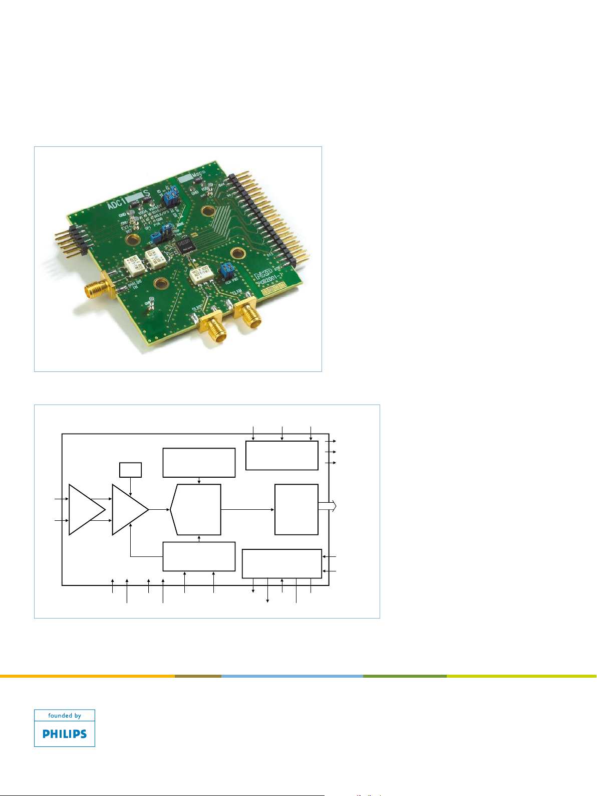
ADC1415S demo board
A programmable gain amplifier lets the ADC accept an input
voltage range from 1 to 2 VPP with a 6-dB programmable fine gain.
ADC1415Sxxx block diagram
www.nxp.com
© 2009 NXP B.V.
All rights reser ved. Reproduc tion i n whol e or in part is p rohibited witho ut the prio r wri tten consent of the co pyright owner.
The informat ion pre sented in this docum ent do es not form part of an y quota tion or contr act, is beli eved to be accurate and
reliabl e an d may be chang ed wi thout notice. No liabilit y wi ll be acce pted by t he pu blisher for any conseque nce of it s us e.
Public ation thereo f does not convey n or imply any lic ense under pat ent- or other ind ustrial or in tellectual p roperty r ights.
www.nxp.com/dataconverters
Date of rel ease: May 200 9
Docum ent order numb er : 9397 750 16732
Printe d in the Netherl ands
 Loading...