

Page 1
Quick Start ADC1002S020
Demonstration board for ADC1002S020
Rev. 2 — 11 octobre 2010 Quick Start
Document information
Info Content
Keywords DEMO8766G, PCB769-2, Demonstration board, ADC, Converter,
ADC1002S020
Abstract This document describes how to use the demonstration board
DEMO8766G for the analog-to-digital converter ADC1002S020.
Overview
Page 2

NXP Semiconductors
Quick Start ADC1002S020
QS ADC1002S020
Contact information
Revision history
Rev Date Description
1 20080612 Initial version.
2 20101011 Update for data acquisition system.
For additional information, please visit: http://www.nxp.com
For sales office addresses, please send an email to: salesaddresses@nxp.com
QS_ADC1002S020_2 All information provided in this document is subject to legal disclaimers. © NXP B.V. 2010. All rights reserved.
Quick Start Rev. 2 — 11 octobre 2010 2 of 24
Page 3
QS ADC1002S020
Quick Start ADC1002S020
Quick Start
QS_ADC1002S020_2
24
P
LOGIC
ANALYZER
C
SYNTHESIZED
I
SYNTHESIZED
F
P
Synchronized
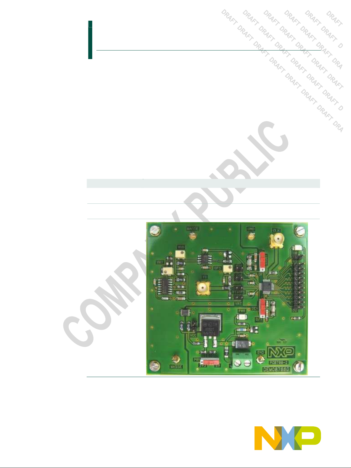
1. Overview of the ADC1002S020 demo board
1.1 ADC1002S020 demoboard
Figure 1 presents the connections to measure the ADC1002S020 based on DEMO8766G:
NXP Semiconductors
SIGNAL
GENERATOR
LOCK SIGNAL
. sinewave
. AC
SIGNAL
Rev. 2 — 11 octobre 2010
GENERATOR
NPUT SIGNAL
. 2 Vpp sinewave
. AC
ILTER
. High-order
. Band pass
Output data:
. D9 (MSB) to D0 (LSB)
RESENTED CONFIGURATION
. 2V
input full scale
pp
. Single TTL-CMOS clock signal
. 3.3 V power supply
. ADC active
DC
OWER SUPPLY
. I = 50 mA
. 12 V
.GND
. Binary ADC output
. VRB = 1.2 V
. VI+OFS = VRM (= 2.25 VDC)
. VRT = 3.3 VDC
Fig 1. ADC1002S020 demoboard set-up
3 of
Page 4
NXP Semiconductors
Quick Start ADC1002S020
QS_ADC1002S020_2
©
NXP B.V.
2010
. All rights reserved.
QS ADC1002S020
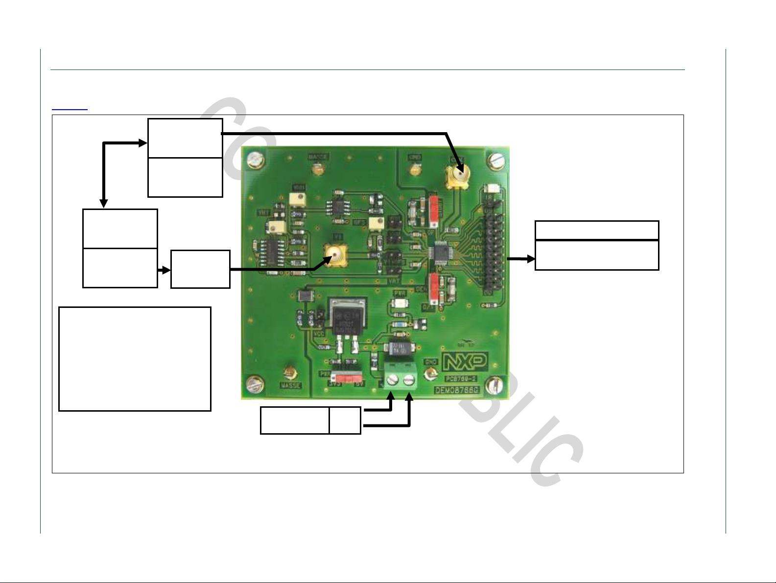
1.2 Power supply
The board is powered with a single 12 VDC power supply. A power supply regulator is
used to supply all the circuitry on the board.
Table 1. General power supply
Name Function View
J3 Green connector – Power supply 12 VDC / 50 mA.
DS2 PWR green light – It indicates the good supply plugging
PWR switch – ADC power supply selection K3
TP31
TM1,
TM2
TM3,
TM4
3.3 V
VCC test point
MASSE test point – Analog ground
GND test point – Digital ground
STDBY switch – ADC stand-by activation K2
ADC active
– ADC power supply
5 V
ADC OFF
1.3 DC voltage adjustments
The ADC1002S020 allows to adjust the full scale input signal from 1.6 V to 2.4 V.
Table 2. DC voltage adjustments
Name Function View
P1 VRT trimmer – TOP reference adjustment
TP1 VRT test point – TOP reference value (typ 3.3 V)
P2 VRB trimmer – BOT reference adjustment
TP5 VRB test point – BOT reference value (typ 1.2 V)
P3 OFS trimmer – Input signal DC offset adjustment
TP3 VI+OFS test point – Input signal DC offset (typ 2.25 V)
TP7 VRM test point – MIDDLE reference value (typ 2.25 V)
Quick Start Rev. 2 — 11 octobre 2010 4 of 24
Page 5
NXP Semiconductors
Quick Start ADC1002S020
QS_ADC1002S020_2
©
NXP B.V.
2010
. All rights reserved.
QS ADC1002S020
1.4 Input signals (VI, CLK)
To ensure a good evaluation of the device, the input signal and the input clock must be
synchronized together.
Moreover, the input frequency (Fi, MHz) and the clock frequency (Fclk, Msps) should
follow the formula:
, where M is an odd number of period and N is the number of samples.
Table 3. Input signals
Name Function View
J2 VI connector – Analog input signal (
J3 CLK connector – Clock input signal (
50Ω
50Ω
matching)
matching)
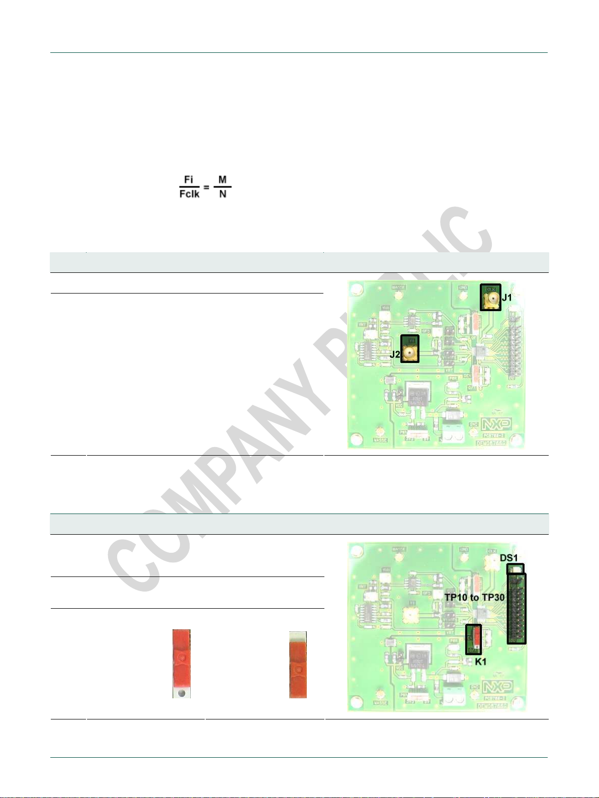
1.5 Output signals (D0 to D9, IR)
Table 4.
Name Function View
TP10
to
TP30
Output signals
Array connector – ADC digital output(D0 to D9) and In
range signal (IR)
DS1 IR green light – It indicates that the analog input signal is
in the full scale range
K1
OEN switch – Output enable selection
Active output
High impedance
output
Quick Start Rev. 2 — 11 octobre 2010 5 of 24
Page 6
QS ADC1002S020
Quick Start ADC1002S020
Quick Start
QS_ADC1002S020_2
24
+5V P
R
SIGNAL
USB
SPI
MODULE
P
. CMOS 2 16
-
bit channels input
LVDS
DDR
I/O
.
up to 325 MHz 16
-
bit LVDS DDR
CMOS
I/O
J
I/O
2. HSDC extension module: acquisition board
The figure 2 shows an overview of the extension module HSDC-EXTMOD01/DB acquisition board:
OWER SUPPLY
. I = 3.2 A
NXP Semiconductors
UMPER FOR
SUPPLY
. define either I/O is 1.8 V or 3.3 V
GENERATOR
Rev. 2 — 11 octobre 2010
EFERENCE SIGNAL
. typical 10 MHz
CONNECTOR
. 2 channels up to 200 MHz 16-bit
RESENTED CONFIGURATION
. acquisition board
. external reference signal
. LVDS DDR 16-bit input stream
CONNECTOR
Fig 2. HSDC extension module: acquisition board
6 of
Page 7
NXP Semiconductors
Quick Start ADC1002S020
QS_ADC1002S020_2
©
NXP B.V.
2010
. All rights reserved.
QS ADC1002S020
The HSDC extension module is intended for acquisition/generation and clock generation
purpose. When connected to an ADC demo-board it is intended as an acquisition system
for digital output bits delivered by ADC, either CMOS (HE14 P1 connector) or LVDS DDR
(SAMTEC QTH_060_02 P2 connector).
The board brief specification is shown below:
• 8MB memory size for acquisition pattern;
• 2 16-bit channels CMOS up to 200 MHz;
• 16-bit LVDS DDR input data stream up to 320 MHz;
• On-board or external reference for signal generation.
In this section the specific requirement for the use with ADC1002S020 demo-board will
be shown.
For more details on the HSDC-EXTMOD01/DB, please contact dataconverter-
support@nxp.com.
2.1 HSDC extension module: hardware initialization
Before using the generation board, make sure that you connect the USB cable prior to
the supply.
2.2 HSDC extension module: software initialization
Before using the generation board, the user needs to install software to control the board.
The steps are described below.
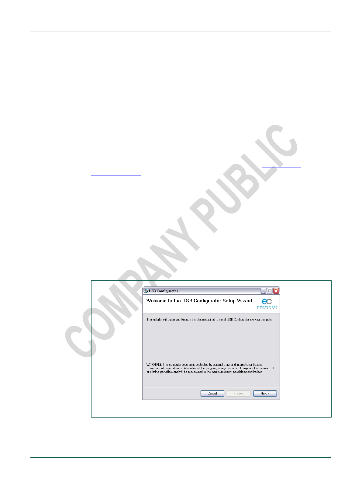
Go to the installation directory “\HSDC-EXTMOD01\Software\USBConfigSetup v1.3
100212 1525” on the CD. Double click on the file “CDM 2.04.16.exe” file.
Run the application “\HSDC-EXTMOD01\Software\USBConfigSetup v1.3 100212
1525\USBConfigSetup.msi”, this will display the following window:
Fig 3. “USBConfigSetup” window: step 1
Click “Next” to proceed with installation process:
Quick Start Rev. 2 — 11 octobre 2010 7 of 24
Page 8
NXP Semiconductors
Quick Start ADC1002S020
QS_ADC1002S020_2
©
NXP B.V.
2010
. All rights reserved.
QS ADC1002S020
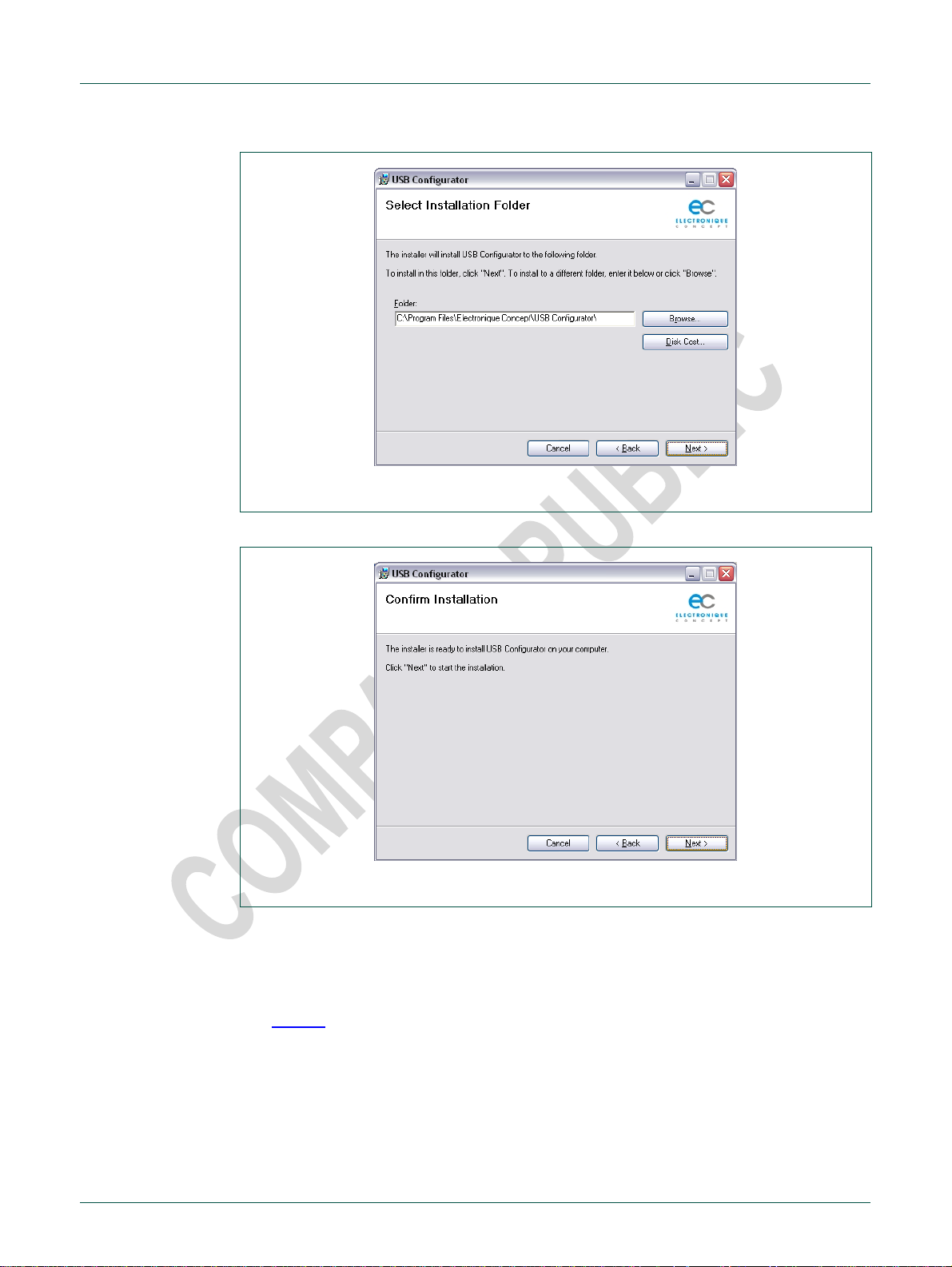
Fig 4. “USBConfigSetup” window: step 2
Click “Next” to continue:
Fig 5. “USBConfigSetup” window: step 3
Click “Next” to finish the installation process.
The system is now ready to use the ADC1412D series board for evaluation purpose.
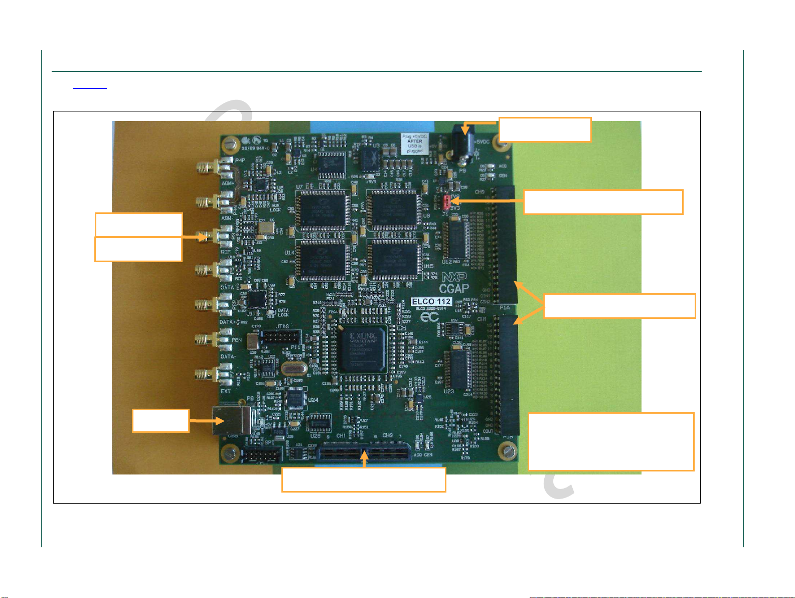
2.3 HSDC extension module: CMOS connector description
The figure 6 shows a brief description of the hardware connection on the HE14
connector:
Quick Start Rev. 2 — 11 octobre 2010 8 of 24
Page 9

NXP Semiconductors
Quick Start ADC1002S020
QS_ADC1002S020_2
©
NXP B.V.
2010
. All rights reserved.
QS ADC1002S020
Fig 6. HSDC extension module: HE14 CMOS hardware schematic overview
The HSDC extension module can acquire data in CMOS level using:
• either the on-board clock generated by the internal PLL, refer to as
pDFS_CLK[0]/nDFS_CLK[0] that will be used by the FPGA. In this case, the
reference of the board should be delivered by the clock signal generator;
Quick Start Rev. 2 — 11 octobre 2010 9 of 24
Page 10

NXP Semiconductors
Quick Start ADC1002S020
QS_ADC1002S020_2
©
NXP B.V.
2010
. All rights reserved.
QS ADC1002S020
• or the clock provided by the ADC refer to as P1_CLK_IN. This is the preferred
situation since the user will not deal with any set-up/hold timing for the acquisition.
Refer to section 3.2 for software configuration.
Quick Start Rev. 2 — 11 octobre 2010 10 of 24
Page 11
QS ADC1002S020
Start ADC1002S020
Quick Start
QS_ADC1002S020_2
24
USB
SPI
MODULE
P
C
HSDC
-
EXTMOD
R
SIGNAL
GENERATOR
+5 V
R
.
e.g 10 MHz
R
EFERENCE
3. Combo ADC1002S020 and HSDC extension module
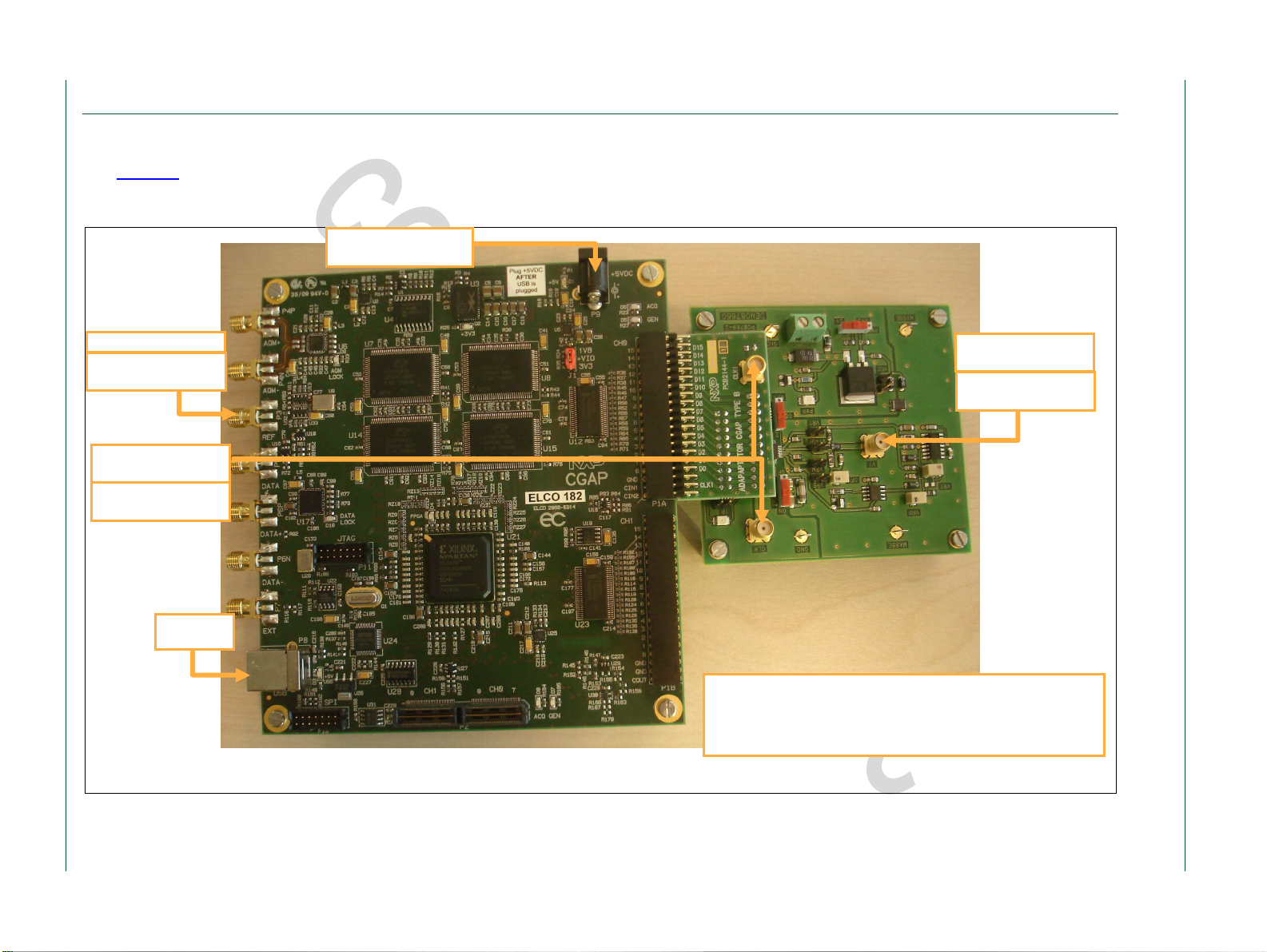
3.1 Measurement set-up overview
The figure 07 below shows an overview of the whole system ADC1002S020+HSDC extension module for which connection is done with the
accessory (HSDC-ACC07/DB). The measurement set-up presented below shows 1 generator for input signal. Clock signal is delivered by the
HSDC-EXTMOD for ADC clocking and data acquisition purpose:
POWER SUPPLY
. I = 3.2 A
EFERENCE SIGNAL
Rev. 2 — 11 octobre 2010
EFERENCE SIGNAL
. e.g 1 MHz
NXP Semiconductors
11 of
CLOCK
LOCK SIGNAL
. e.g 20 Msps
Fig 7. Evaluation set-up measurement with ADC1002S020 and HSDC-EXTMOD01/DB
RESENTED CONFIGURATION
. Single-ended clock on CLK
. 2 V
input full scale
pp
. Signal generator synchronized with HSDC-EXTMOD
Quick
Page 12

NXP Semiconductors
Quick Start ADC1002S020
QS ADC1002S020
3.2 HSDC extension module: FPGA flash
To get access to the software control of the generation system, run the “USB
Configurator.exe”. It is located by default in the directory "C:\Program Files\Electronique
Concept\USB Configurator\".
If a HSDC extension module is connected to the user system it will display the following
window:
Fig 8. “USB Configurator” window: board main control
This window gives an overview of the current status of the board connected. If supply is
not connected, a FAIL status appears on the Power status field.
Flash the FPGA with the appropriate bin file provided on the CD located at “\HSDCEXTMOD01\Software\USBConfigSetup v1.3 100212 1525\HSDCEXTMOD FPGA bin
v03”. Among the 8 files, 2 are considered here:
• “HSDCEXTMOD_v03_P1C_RE_3V3_GEN.bin”: the FPGA will use the rising edge
of the clock delivered by connector P1C;
• “HSDCEXTMOD _v03_P1C_FE_3V3_ACQ.bin”: the FPGA will use the falling edge
of the clock delivered by connector P1C.
For further details regarding the others file please contact dataconverter-
support@nxp.com.
Browse to select the wanted bin file. Click “Erase” and “Program” buttons. Once the
“Successful” message appears, click “Reset FPGA” button: board is programmed.
3.3 HSDC extension module: DATA clock configuration
To acquire the digital input pattern on P1 connector, the user needs to choose the
wanted frequency. In our example, the frequency used for acquisition is 20 MHz and the
reference signal is provided on external “REF” pin:
QS_ADC1002S020_2 All information provided in this document is subject to legal disclaimers. © NXP B.V. 2010. All rights reserved.
Quick Start Rev. 2 — 11 octobre 2010 12 of 24
Page 13

NXP Semiconductors
Quick Start ADC1002S020
QS ADC1002S020
Fig 9. “USB Configurator” window: DATA clock configuration
The FPGA configuration indicates which configuration file has been programmed in
FPGA, in the example shown it is the rising edge of the embedded clock.
In the directory “\HSDC-EXTMOD01\Software\USBConfigSetup v1.3 100212
1525\Config” of the CD, there are 2 configurations files that already defines frequencies
for the DFS and AFS (AQM clock configuration that we don’t use here). Copy these files
to the directory “C:\Documents and Settings\All Users\Application Data\Electronique
Concept\UsbConfig” to get access to these frequencies.
Select “LMK03001 20 MHz – 20 MHz (20.000 MHz)” to define the frequency to be 20
MHz. The pattern will be acquired as this sampling rate, meaning 20 MHz CMOS.
Click “Update”, this should display 6 green check boxes and the value of the
corresponding frequency being actually generated by the board.
The Data Phase Shift allows the user to shift the clock position wrt data by the amount of
time indicated.
Note: you can edit the LMK file by clicking on the “Edit…” button to define your own
frequency, as long as you respect the frequency range defined by the PLL. For other
frequencies to generate, please contact dataconverter-support@nxp.com for more
details.
3.4 HSDC extension module: pattern acquisition
The clock frequency is defined, and the board is ready to acquire the pattern.
In order to do the acquisition, the number of samples needs to be filled in the Pattern size
field: this number is a power of 2 with a maximum of 8MB.
Select one-shot mode and source P1 to acquire data (see figure 10).
The hardware connection between the ADC1002S020 and the HSDC extension module
has to be described to get correct results. This is done by using the fields in “Channel 0
Input Configuration” and in “Channel 1 Input Configuration”.
The channel 0 receives the data from ADC where ADC MSB is connected to the 1st bit
and ADC LSB is connected to the 10th bit of the HSDC extension module. Tune the fields
“Input is located on file A between xx (MSB) and xx (LSB)” to describe this configuration
(see figure 10).
QS_ADC1002S020_2 All information provided in this document is subject to legal disclaimers. © NXP B.V. 2010. All rights reserved.
Quick Start Rev. 2 — 11 octobre 2010 13 of 24
Page 14

NXP Semiconductors
Quick Start ADC1002S020
QS ADC1002S020
Fig 10. “USB Configurator” window: pattern acquisition for ADC1002S020
3.4.1 Pattern acquisition
Browse on both channel path configuration to select the file to store the data that will be
acquired.
Click on “Acquire” and “Save” buttons to end the capture process.
3.5 FFT post-processing
Once acquisition is done, the captured data can now be processed for FFT results using
the “NXP_ADC_Acquisition.exe” tool located under directory “\HSDCEXTMOD01\Software\NXP_ADC_Acquisition” of the CD.
Run the application it will display the following window:
QS_ADC1002S020_2 All information provided in this document is subject to legal disclaimers. © NXP B.V. 2010. All rights reserved.
Quick Start Rev. 2 — 11 octobre 2010 14 of 24
Page 15

NXP Semiconductors
Quick Start ADC1002S020
QS ADC1002S020
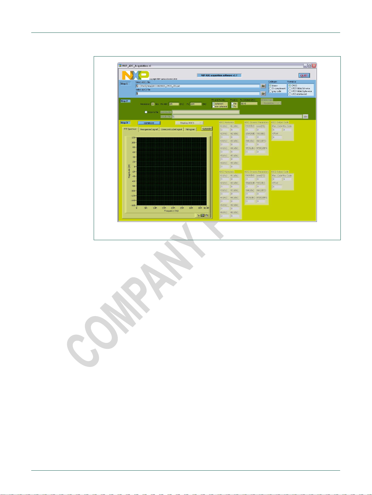
Fig 11. “NXP_ADC_Acquisition” window: start-up screen
3.5.1 Acquisition software: input files
The first step consists in delivering the files to be processed. Browse in field “Select
ADC1 file:” to indicate the file to be used.
Indicate the data format (by default data are stored in binary format).
Note: both files needs to have the same data format and have the same input and clock
frequency.
Indicate CMOS mode.
3.5.2 Acquisition software: frequency indication
The second step consists in indicating the relevant numbers for the FFT processing:
• the resolution N: 10 in this case;
• the input frequency Fin: 1.25 MHz in our example;
• the sampling frequency Fs: 20 Msps in our example;
• whether Fin or Fs are coherent or not:
− if signals are coherent, selected which Fin or Fs are fixed for the calculation (see
appendix A.1). The value of coherent frequency resulting from this calculation will
be displayed (this corresponds to the value to be generated in front of the ADC);
− if signals are not coherent, select the window for FFT processing to apply (the
Blackman window gives better results).
The example shown below is for Fin = 1.25 MHz Fs = 20 Msps, with Fin and Fs coherent
and Fs fixed value in CMOS mode:
QS_ADC1002S020_2 All information provided in this document is subject to legal disclaimers. © NXP B.V. 2010. All rights reserved.
Quick Start Rev. 2 — 11 octobre 2010 15 of 24
Page 16
NXP Semiconductors
Quick Start ADC1002S020
QS ADC1002S020
Fig 12. “NXP_ADC_Acquisition” window: frequency entry
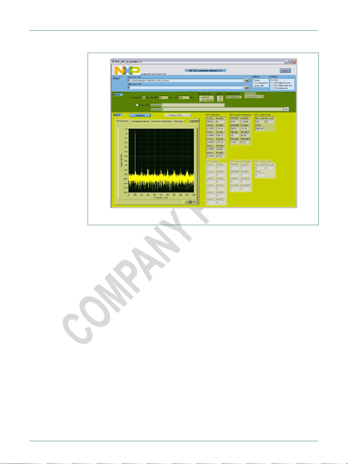
3.5.3 Acquisition software: FFT results display
Press the “COMPUTE” button to display the results from the FFT processing. The results
fields will be updated depending on the number of input files. If 2 files have been
processed, it is possible to display both results on the same picture for all graphs using
the “Display …” button (“Display ADC1” or “Display ADC2” or “Display ADC1 & ADC2”).
3.5.3.1 FFT spectrum
The first graph to be displayed is the FFT spectrum of the digital pattern acquired:
QS_ADC1002S020_2 All information provided in this document is subject to legal disclaimers. © NXP B.V. 2010. All rights reserved.
Quick Start Rev. 2 — 11 octobre 2010 16 of 24
Page 17
NXP Semiconductors
Quick Start ADC1002S020
QS ADC1002S020
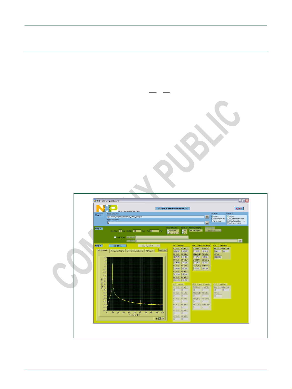
Fig 13. “NXP_ADC_Acquisition” window: FFT result
Press the “Autoscale” button to display the whole content.
The tables and give the relevant dynamic parameters:
• Table : first 6 harmonics frequencies and amplitude level;
• Table : dynamics parameters:
− ENOB expressed in bit;
− Level of the digital output signal relative to the full-scale;
− SINAD in dBc;
− THD in dBc calculated over first 6 harmonics;
− SNR in dBc and dBFS;
− SFDR in dBc and dBFS.
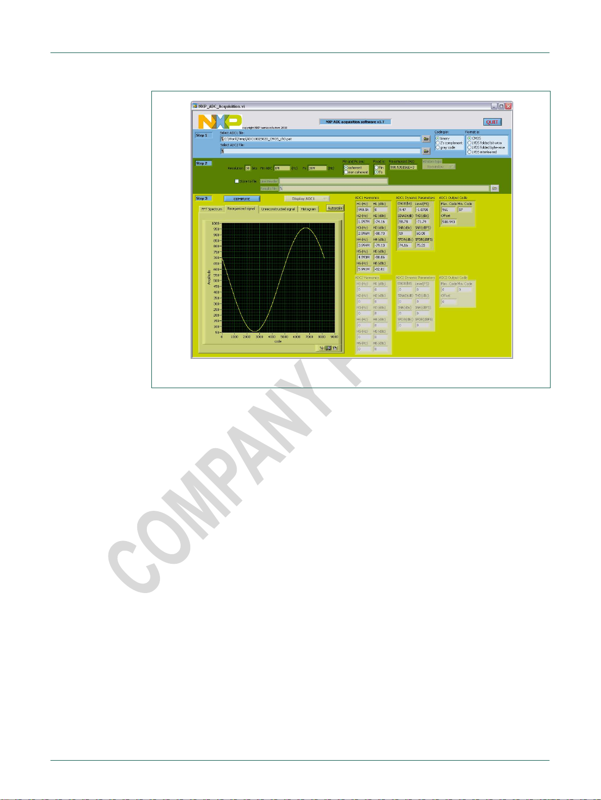
3.5.3.2 Reorganized signal
The Reorganized signal displays the reconstructed sine wave from coherency calculation
corresponding to 1 period of the input signal:
QS_ADC1002S020_2 All information provided in this document is subject to legal disclaimers. © NXP B.V. 2010. All rights reserved.
Quick Start Rev. 2 — 11 octobre 2010 17 of 24
Page 18
NXP Semiconductors
Quick Start ADC1002S020
QS ADC1002S020
Fig 14. “NXP_ADC_Acquisition” window: reorganized signal
Press the “Autoscale” button to display the whole content.
3.5.3.3 Unreconstruted signal
The unreconstructed signal displays the unreconstructed sine wave corresponding to the
whole number of period being acquired following the coherency rule:
QS_ADC1002S020_2 All information provided in this document is subject to legal disclaimers. © NXP B.V. 2010. All rights reserved.
Quick Start Rev. 2 — 11 octobre 2010 18 of 24
Page 19

NXP Semiconductors
Quick Start ADC1002S020
Zoom tool
QS ADC1002S020
Fig 15. “NXP_ADC_Acquisition” window: unreconstruted signal
Press the “Autoscale” button to display the whole content.
Use the zoom tool to observe in more details all the captured data.
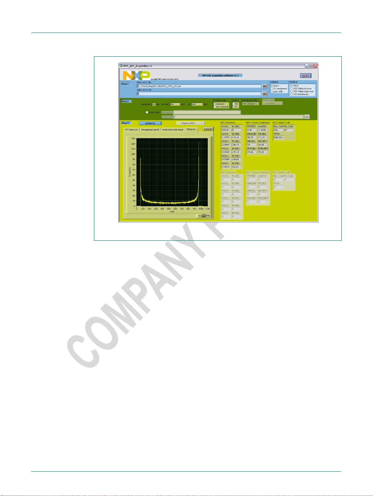
3.5.3.4 Histogram
The histogram graph shows the distribution of output codes. This graph allows to know
which code is present and if there is any missing code in the conversion range:
QS_ADC1002S020_2 All information provided in this document is subject to legal disclaimers. © NXP B.V. 2010. All rights reserved.
Quick Start Rev. 2 — 11 octobre 2010 19 of 24
Page 20
NXP Semiconductors
Quick Start ADC1002S020
QS ADC1002S020
Fig 16. “NXP_ADC_Acquisition” window: code histogram
Press the “Autoscale” button to display the whole content.
The table shows the range of output codes.
QS_ADC1002S020_2 All information provided in this document is subject to legal disclaimers. © NXP B.V. 2010. All rights reserved.
Quick Start Rev. 2 — 11 octobre 2010 20 of 24
Page 21
NXP Semiconductors
Quick Start ADC1002S020
QS ADC1002S020
4. Appendix A.1: coherency calculation
The coherency relies on the fact that clock and analog input signal are synchronized and
the first and last samples being captured are adjoining samples: it ensures a continuous
digitized time process for the FFT processing.
To achieve this, one has to follow the equation:
where M is an odd integer equal to the number of periods being acquired and N the
number of samples acquired.
With Fin, Fs and N known, M has to be chosen such that it follows the equation above.
To do this iterative calculation, one has to decide whether Fin or Fs is fixed.
To illustrate this process, let’s consider our current example with Fin = 1 MHz, Fs = 20
Msps and N = 8192 samples acquired:
• if Fin is fixed, this leads to M = 409 periods of input signal to be acquired and a real
sampling frequency to be Fs = 20.0293399 MHz;
• if Fs is fixed, this leads to M = 409 periods of input signal to be acquired and a real
input frequency to be Fin = 0.998535156 MHz.
Those values needs to be programmed in the signal generator and clock generator
before capture is done, otherwise the FFT calculation will lead to a non-coherent result
as shown below:
M
F
in
=
N
F
s
Fig 17. “NXP_ADC_Acquisition” window: non-coherent capture example
The numbers given for SNR, SFDR are completely wrong if coherency is not respected.
QS_ADC1002S020_2 All information provided in this document is subject to legal disclaimers. © NXP B.V. 2010. All rights reserved.
Quick Start Rev. 2 — 11 octobre 2010 21 of 24
Page 22

NXP Semiconductors
Quick Start ADC1002S020
QS ADC1002S020
5. Notes
For any question, feel free to contact us at the following e-mail dataconverter-
support@nxp.com.
QS_ADC1002S020_2 All information provided in this document is subject to legal disclaimers. © NXP B.V. 2010. All rights reserved.
Quick Start Rev. 2 — 11 octobre 2010 22 of 24
Page 23

NXP Semiconductors
Quick Start ADC1002S020
QS ADC1002S020
6. Legal information
Semiconductors products in order to avoid a default of the applications and
6.1 Definitions
Draft — The document is a draft version only. The content is still under
internal review and subject to formal approval, which may result in
modifications or additions. NXP Semiconductors does not give any
representations or warranties as to the accuracy or completeness of
information included herein and shall have no liability for the consequences
of use of such information.
6.2 Disclaimers
Limited warranty and liability — Information in this document is believed to
be accurate and reliable. However, NXP Semiconductors does not give any
representations or warranties, expressed or implied, as to the accuracy or
completeness of such information and shall have no liability for the
consequences of use of such information.
In no event shall NXP Semiconductors be liable for any indirect, incidental,
punitive, special or consequential damages (including - without limitation lost profits, lost savings, business interruption, costs related to the removal
or replacement of any products or rework charges) whether or not such
damages are based on tort (including negligence), warranty, breach of
contract or any other legal theory.
Notwithstanding any damages that customer might incur for any reason
whatsoever, NXP Semiconductors’ aggregate and cumulative liability
towards customer for the products described herein shall be limited in
accordance with the Terms and conditions of commercial sale of NXP
Semiconductors.
Right to make changes — NXP Semiconductors reserves the right to make
changes to information published in this document, including without
limitation specifications and product descriptions, at any time and without
notice. This document supersedes and replaces all information supplied prior
to the publication hereof.
Suitability for use — NXP Semiconductors products are not designed,
authorized or warranted to be suitable for use in life support, life-critical or
safety-critical systems or equipment, nor in applications where failure or
malfunction of an NXP Semiconductors product can reasonably be expected
to result in personal injury, death or severe property or environmental
damage. NXP Semiconductors accepts no liability for inclusion and/or use of
NXP Semiconductors products in such equipment or applications and
therefore such inclusion and/or use is at the customer’s own risk.
Applications — Applications that are described herein for any of these
products are for illustrative purposes only. NXP Semiconductors makes no
representation or warranty that such applications will be suitable for the
specified use without further testing or modification.
Customers are responsible for the design and operation of their applications
and products using NXP Semiconductors products, and NXP
Semiconductors accepts no liability for any assistance with applications or
customer product design. It is customer’s sole responsibility to determine
whether the NXP Semiconductors product is suitable and fit for the
customer’s applications and products planned, as well as for the planned
application and use of customer’s third party customer(s). Customers should
provide appropriate design and operating safeguards to minimize the risks
associated with their applications and products.
NXP Semiconductors does not accept any liability related to any default,
damage, costs or problem which is based on any weakness or default in the
customer’s applications or products, or the application or use by customer’s
third party customer(s). Customer is responsible for doing all necessary
testing for the customer’s applications and products using NXP
the products or of the application or use by customer’s third party
customer(s). NXP does not accept any liability in this respect.
Export control — This document as well as the item(s) described herein
may be subject to export control regulations. Export might require a prior
authorization from national authorities.
Evaluation products — This product is provided on an “as is” and “with all
faults” basis for evaluation purposes only. NXP Semiconductors, its affiliates
and their suppliers expressly disclaim all warranties, whether express,
implied or statutory, including but not limited to the implied warranties of noninfringement, merchantability and fitness for a particular purpose. The entire
risk as to the quality, or arising out of the use or performance, of this product
remains with customer.
In no event shall NXP Semiconductors, its affiliates or their suppliers be
liable to customer for any special, indirect, consequential, punitive or
incidental damages (including without limitation damages for loss of
business, business interruption, loss of use, loss of data or information, and
the like) arising out the use of or inability to use the product, whether or not
based on tort (including negligence), strict liability, breach of contract, breach
of warranty or any other theory, even if advised of the possibility of such
damages.
Notwithstanding any damages that customer might incur for any reason
whatsoever (including without limitation, all damages referenced above and
all direct or general damages), the entire liability of NXP Semiconductors, its
affiliates and their suppliers and customer’s exclusive remedy for all of the
foregoing shall be limited to actual damages incurred by customer based on
reasonable reliance up to the greater of the amount actually paid by
customer for the product or five dollars (US$5.00). The foregoing limitations,
exclusions and disclaimers shall apply to the maximum extent permitted by
applicable law, even if any remedy fails of its essential purpose.
6.3 Licenses
Purchase of NXP <xxx> components
<License statement text>
6.4 Patents
Notice is herewith given that the subject device uses one or more of the
following patents and that each of these patents may have corresponding
patents in other jurisdictions.
<Patent ID> — owned by <Company name>
6.5 Trademarks
Notice: All referenced brands, product names, service names and
trademarks are property of their respective owners.
<Name> — is a trademark of NXP B.V.
QS_ADC1002S020_2 All information provided in this document is subject to legal disclaimers. © NXP B.V. 2010. All rights reserved.
Quick Start Rev. 2 — 11 octobre 2010 23 of 24
Page 24

NXP Semiconductors
Quick Start ADC1002S020
11 octobre 2010
QS_ADC1002S020_2
QS ADC1002S020
7. Contents
1.
Overview of the ADC1002S020 demo board .....3
1.1
ADC1002S020 demoboard................................3
1.2
Power supply......................................................4
1.3
DC voltage adjustments.....................................4
1.4
Input signals (VI, CLK) .......................................5
1.5
Output signals (D0 to D9, IR).............................5
2.
HSDC extension module: acquisition board.....6
2.1
HSDC extension module: hardware initialization7
2.2
HSDC extension module: software initialization.7
2.3
HSDC extension module: CMOS connector
description..........................................................8
3.
Combo ADC1002S020 and HSDC extension
module ...............................................................11
3.1
Measurement set-up overview.........................11
3.2
HSDC extension module: FPGA flash..............12
3.3
HSDC extension module: DATA clock
configuration.....................................................12
3.4
HSDC extension module: pattern acquisition...13
3.4.1
Pattern acquisition............................................14
3.5
FFT post-processing ........................................14
3.5.1
Acquisition software: input files........................15
3.5.2
Acquisition software: frequency indication .......15
3.5.3
Acquisition software: FFT results display.........16
3.5.3.1 FFT spectrum...................................................16
3.5.3.2 Reorganized signal ..........................................17
3.5.3.3 Unreconstruted signal ......................................18
3.5.3.4 Histogram.........................................................19
4.
Appendix A.1: coherency calculation..............21
5.
Notes ..................................................................22
6.
Legal information ..............................................23
6.1
Definitions ........................................................23
6.2
Disclaimers.......................................................23
6.3
Licenses...........................................................23
6.4
Patents.............................................................23
6.5
Trademarks......................................................23
7.
Contents.............................................................24
Please be aware that important notices concerning this document and the product(s)
described herein, have been included in the section 'Legal information'.
© NXP B.V. 2010. All rights reserved.
For more information, please visit: http://www.nxp.com
For sales office addresses, please send an email to: salesaddresses@nxp.com
Date of release:
Document identifier:
 Loading...