

Page 1

Embedded COM System
User‘s Manual
Product Number:
21265-010/020/030
Doc-No: 63972-366_R1.5
April 2018
Page 2

R1.5 April 2018 rebranded
Impressum:
Schroff GmbH
Langenalber Str. 96 - 100
75334 Straubenhardt, Germany
The details in this manual have been carefully compiled and
checked - supported by certified Quality Management System
to EN ISO 9001/2000
The company cannot accept any liability for errors or misprints.
The company reserves the right to amendments of technical
specifications due to further development and improvement of
products.
Copyright2018
All rights and technical modifications reserved.
Page 3

21265-010/020/030
Table of Contents
1 Safety .................................................................................................................................... 1
1.1 Safety Symbols used in this document ........................................................................... 1
1.2 General Safety Precautions................................................................................................ 1
1.3 References and Architecture Specifications................................................................... 1
2 Introduction.......................................................................................................................... 2
2.1 Schroff Embedded COM System ...................................................................................... 2
2.2 System Overview.................................................................................................................. 3
2.3 Disassemble the Case......................................................................................................... 7
2.4 Schroff Carrier Board........................................................................................................... 8
2.5 COM Carrier........................................................................................................................... 9
2.6 Fixing Post Layout.............................................................................................................. 10
2.7 COM Carrier Connector and Jumper Overview............................................................ 11
2.8 Jumper Settings Overview ............................................................................................... 12
2.9 Connector Overview .......................................................................................................... 13
2.10 Signal Routing..................................................................................................................... 14
3 Power .................................................................................................................................. 15
3.1 Power Input ......................................................................................................................... 15
3.2 Power Connectors and Jumpers .................................................................................... 16
4 Interfaces ........................................................................................................................... 17
4.1 LPC Super I/O Controller................................................................................................... 17
4.2 Serial Interfaces.................................................................................................................. 17
4.3 Parallel Interface................................................................................................................. 18
4.4 I2C-Bus, SMBus and CAN Interfaces ............................................................................. 18
4.5 SPI Flash EEPROM............................................................................................................. 19
4.6 USB ....................................................................................................................................... 20
4.7 Ethernet................................................................................................................................ 20
4.8 SATA ..................................................................................................................................... 20
4.9 PCI Express ......................................................................................................................... 21
4.10 MiniPCIe............................................................................................................................... 21
4.11 XMC ...................................................................................................................................... 22
4.12 XMC I/O Plug-on Module .................................................................................................. 23
4.13 Fieldbus Interface............................................................................................................... 24
4.14 LVDS Interface.................................................................................................................... 25
4.15 Prototype Interface ............................................................................................................ 26
4.16 Fan Control.......................................................................................................................... 27
4.17 Audio Interfaces ................................................................................................................. 28
4.18 Video Interfaces ................................................................................................................. 29
5 Technical Data................................................................................................................... 30
I R1.5, April 2018
Page 4

21265-010/020/030
II R1.5, April 2018
Page 5

1 Safety
The intended audience of this User’s Manual is system integrators and hardware/software
engineers.
1.1 Safety Symbols used in this document
Caution!
This is the user caution symbol. It indicates a condition where damage of the equipment or
injury of the service personnel could occur. To reduce the risk of damage or injury, follow all
steps or procedures as instructed.
Danger of electrostatic discharge!
The COM Carrier contains static sensitive devices. To prevent static damage you must wear
an ESD wrist strap.
21265-010/020/030
1.2 General Safety Precautions
• Service personnel must know the necessary electrical safety, wiring and connection
practices for installing this equipment.
• Install this equipment only in compliance with local and national electrical codes.
1.3 References and Architecture Specifications
• PICMG® COM Express Module™ Base Specification
(www.pigmg.org)
• PICMG® COM Express® Carrier Design Guide
(www.pigmg.org)
Safety 1 R1.5, April 2018
Page 6

2 Introduction
COM Express® is a PICMG® standard that describes a COM (Computer-On-Module) and the
supporting Carrier Board.
• The COM contains the processor, RAM, and I/O ICs.
• The Carrier Board provides power to the COM, additional I/O ICs, and all of the
I/O connections.
Together the COM and Carrier Board make a bootable computer.
The electrical and mechanical interface between the COM and Carrier Board has several
“Type” definitions. The user can select a COM and Carrier Board with an interface Type that
matches their requirements.
2.1 Schroff Embedded COM System
The Schroff Embedded COM Systems combine Schroff COM Carrier boards and COM Express
Type 6 modules in an Interscale case with convection cooling including a power board with
18 VDC - 26,4 VDC input voltage.
21265-010/020/030
• 21265-010: Embedded COM System with congatec conga-TC170/3955U (045203)
COM Express Type 6 Compact module with Intel® Celeron® 3955U dual core processor
with 2.0 GHz, 2 MB L2 cache and 2133 MT/s dual channel DDR4 memory interface
• 21265-020: Embedded COM System with congatec conga-TS170/i7-6820EQ (045900)
COM Express Type 6 Basic module with Intel® Core™ i7-6820EQ quad core processor with
2.8 GHz up to 3.5 GHz, 8MB L2 cache, GT2 graphics and 2133 MT/s dual channel DDR4
memory interface, Chipset QM170
• 21265-030: Embedded COM Lab System with slots/connectors for prototype and XMC
modules and congatec conga-TS170/i7-6820EQ (045900) COM Express Type 6 Basic
module with Intel® Core™ i7-6820EQ quad core processor with 2.8 GHz up to 3.5 GHz, 8
MB L2 cache, GT2 graphics and 2133 MT/s dual channel DDR4 memory interface,
Chipset QM170
All systems come with a power board generating the COM Carrier supply voltages
(1.5 V, 3.3 V, 5 V, 12 V) from the system input voltage (18 - 26,4 VDC)
Introduction 2 R1.5, April 2018
Page 7
2.2 System Overview
21265-010/020/030
Type 6 Compact module with Intel® Celeron® 3955U dual
core processor;
4 GB DDR4-SODIMM-2400
Type 6 Basic module with Intel® Core™ i7-6820EQ quad core
processor;
8 GB DDR4-SODIMM-2400
SSD 120 GB SATA
Power/Data Cable for Hard Disk
COM Carrier (partly assembled w/o XMC and Prototype con-
nectors)
COM Carrier (fully equipped with XMC and Prototype con-
nectors)
Slot for an optional XMC Module at the right side covered
with a dummy panel
Slot for an optional Fieldbus Module at the rear side covered
with a dummy panel
Heatsink medium power
Heatsink high power
Front Panel Connectors:*
DVI
2x Display Port
4x USB 3.0
S/PDIF Optical
HD audio I/O
Gigabit Ethernet UTP
Rear Panel Connectors:*
15-pin VGA
Serial Port (DSUB9)
Power
21265-010
Embedded COM
System
X
X X X
X X X
X X
X X X
X
X X X
X X X
21265-020
Embedded COM
System
X X
X X
21265-030
Embedded COM
Lab System
X
X
Connectors/slots on PCB:*
X X X
2x MiniPCI Express
Fieldbus Module connector
LVDS Module co nn ector
PCI Express slot with 4x PCIe
3x SATA ports
2x Micro SIMM
1 serial port
Parallel printer port
1x MicroSD
Speaker
Interface for POST code display
XMC Module Connector
X
XMC I/O Plug-on Module Connector
Prototype Module Connector
Fan for XMC Module
X
* Interfaces supported by the pre-assembled COM Modules see Figure 1
Introduction 3 R1.5, April 2018
Page 8

Figure 1: Interfaces supported by the COM Modules
21265-010/020/030
Introduction 4 R1.5, April 2018
Page 9

Figure 2: Embedded COM Systems
21265-010/020/030
1 Embedded COM System (Celeron) 5 Air inlet
2 Embedded COM System (i7) 6 Power input
3 Embedded COM Lab System 7 Slot for optional Fieldbus Module
4 Slot for XMC Module
Introduction 5 R1.5, April 2018
Page 10

Figure 3: Embedded COM Systems Overview
21265-010/020/030
1 Fan for XMC Module (Optional) 4 Heatsink (Large for i7 COM Modules)
2 XMC Module (Example, not scope of delivery) 5 Heatsink (Small fpr Celeron COM Modules)
3 Power Module 6 Heatsink (Fixing Screws)
Introduction 6 R1.5, April 2018
Page 11

2.3 Disassemble the Case
Figure 4: Disassemble the Case
21265-010/020/030
Disassemble the case:
• Remove the 2 screws (1)
• Pull the frontpanel (2) forwards
• Remove the screws (3)
• Remove the heatsink (4)
• Pull the top cover (5) upwards
Introduction 7 R1.5, April 2018
Page 12

2.4 Schroff Carrier Board
The Schroff COMET6 Carrier Board supports the Type-6 interface definition described in the
PICMG COM Express Module Base Specification, and can be used with any Type-6 COM.
This allows the user to select a Type-6 COM with as much or as little processing power as
needed for the specific application. The COMET6 Carrier Board can be used as is in an
application, or as the basis for a custom application specific Carrier Board design.
21265-010/020/030
The Schroff COMET6 Carrier Board is designed for Compact- or Basic-sized
COM Modules and supports the Type-6 interface.
Interfaces:
• 2x MiniPCI Express modules with USB, one with mSATA
• Fieldbus Module for developing interfaces such as CAN or second ethernet
• LVDS Display Module
• XMC Module
• XMC I/O Plug-on Module
• PCI Express slot with PCIe x4
•3x SATA ports
• Gigabit Ethernet UTP
• 3x serial ports
• Parallel printer port
•MicroSD
• 15-pin VGA
•DVI
•2x Display Port
• 1x USB 2.0 and 4x USB 3.0
•S/PDIF Optical
• HD audio I/O
•Speaker
• Interface for POST code display
• The COMET6 Carrier Board also includes a socket for a SPI flash device that can be used
for BIOS expansion, and a 32 kbyte I2C SEEPROM
Introduction 8 R1.5, April 2018
Page 13

2.5 COM Carrier
Figure 5: COM Carrier with Power Module
21265-010/020/030
Introduction 9 R1.5, April 2018
Page 14
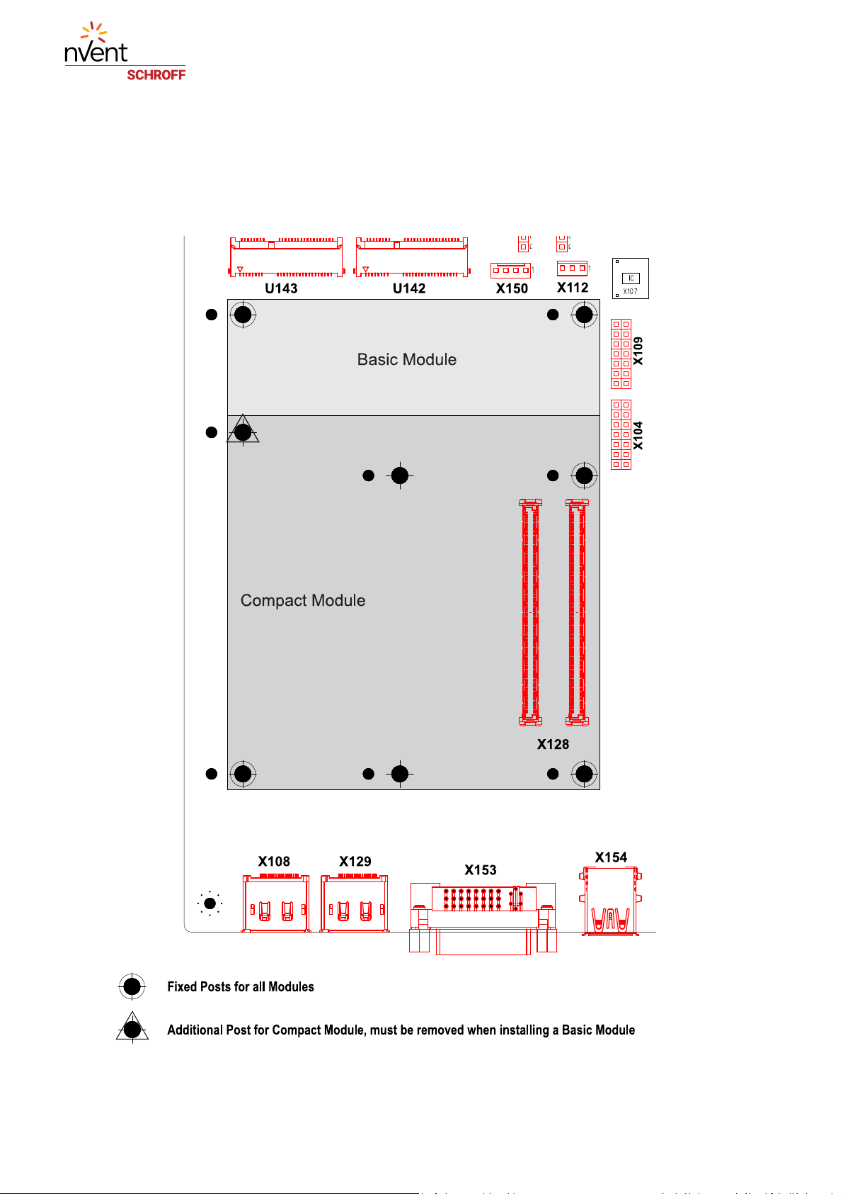
2.6 Fixing Post Layout
When the factory-installed COM Module is replaced by an Module with a different form
factor, some fixing posts mus be removed or added.
Figure 6: Fixing Post Layout
21265-010/020/030
Introduction 10 R1.5, April 2018
Page 15

2.7 COM Carrier Connector and Jumper Overview
Figure 7: COM Carrier Connector and Jumper Overview
21265-010/020/030
Blue: Jumper
Red: Connector
Introduction 11 R1.5, April 2018
Page 16

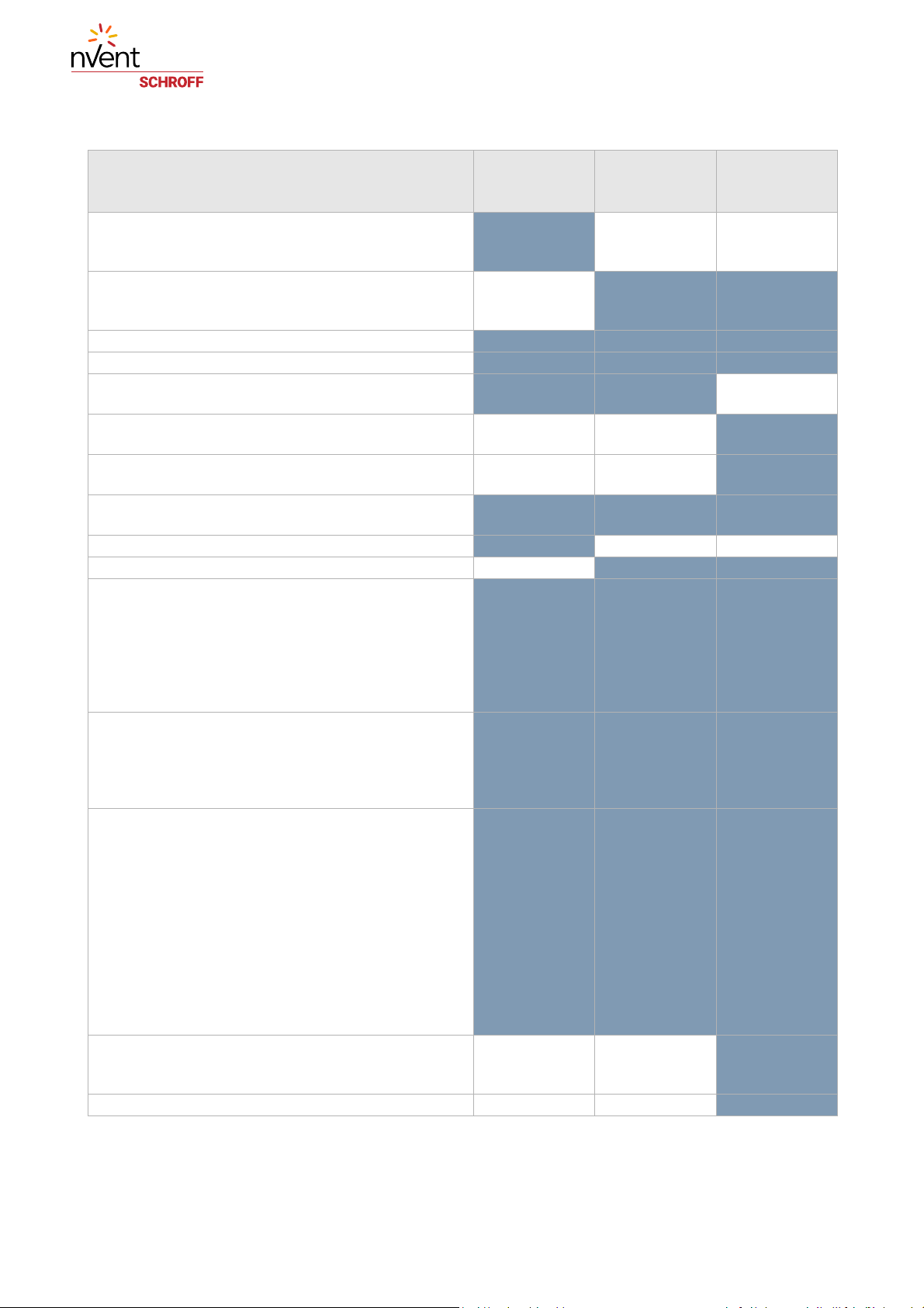
2.8 Jumper Settings Overview
Jumper Settings
X110
X111
X113
X115
X116
X117
X120
X124
X138
X161
Vcc to U SB 1-2: Vcc to USB in Suspend State 4 (COM Express Module)
Incorrect COM Module Type will disable Vcc
SDcard Selection 1-2: AEN# MicroSD in Socket X140
BIOS Selection Strap 1-2: Connects BIOS_DIS0# to ground
BIOS Selection Strap 1-2: Connects BIOS_DIS1# to ground
SPI Power Selection 1-2: Connects SPI_POWER to pin 5 of X109
XMC Power Selection 1-2: connects VCC_12V to XMC
Serial port on DB9 connector X136 1-2 & 7-8 for Serial Port B on Super I/O
Disable Vcc in a Suspend State 1-2: Always Enable Vcc
Super I/O Oscillator frequency 1-2: Super I/O Oscillator frequency = 48 MHz
1-2: Incorrect COM Module Type will disable Vcc (COM Express Module)
2-3: Incorrect COM Module Type will not disable Vcc
2-3: BEN# GPIO on Prototype Module
2-3 or no jumper connects VCC_5V0 to XMC
3-4 & 5-6 for Serial Port 0 on COM Module
3-4: Disable Vcc in Suspend State 3
5-6: Disable Vcc in Suspend State 4
7-8: Disable Vcc in Suspend State 5
2-3: Super I/O Oscillator frequency = 24 MHz
21265-010/020/030
Introduction 12 R1.5, April 2018
Page 17

2.9 Connector Overview
Connector
U103 PCIe [0-3] x4 Card Edge
U142 Mini PCIe, 52-pin, PCIe #5, USB2 #7, Micro SIMM socket on X126
U143 Mini PCIe, 52-pin, PCIe #4/SATA #0, USB2 #6, Micro SIMM socket on X127
X100 XMC J16
X101 XMC I/O Plug-on Module
X102 XMC J15
X103 Power for XMC I/O Plug-on Module
X104 POST Code Module
X105 Serial A from the Super I/O
X106 I²C-Bus, SMBus, CAN Bus
X107 SPI Flash Device socket
X108 Display Port
X109 SPI Programming Port
X112 4-Wire Fan with control from SuperI/O (LPC)*
X118 3-Wire Fan with control from the COM Module
X119 USB0, USB1, and Ethernet
X121 Connector NTC Temperature Sensor from Super IO
X122 Speaker
X125 USB #5 Host
X126 Micro SIMM #1 socket for Mini PCIe on U142
X127 Micro SIMM #2 socket for Mini PCIe on U143
X128 Type-6 COM Express Module
X129 Display Port
X130 Parallel Printer Port from Super I/O
X131 SATA Port #1
X132 SATA Port #2
X133 SATA Port #3
X134 Ground for test probe
X135 Input ext. -12 V for XMC J15
X136 DB-9 Serial
X140 MicroSD Socket
X142 Disk Drive Power
X143 Fieldbus Module
X144 LVDS Module
X145 Prototype Module
X146 Power Board
X148 XMC Module JTAG
X149 VGA
X150 4-Wire Fan with control from the COM Module
X151 HD Audio
X153 DVI
X154 USB #2 and #3
X156 Current measurement shunt for +5.0 V Standby on COM Module
X157 Current measurement shunt for +12.0 V on COM Module
X158 Current measurement shunt for +3.3 V Standby
X159 Current measurement shunt for +5.0 V Standby
X160 Current measurement shunt for +12.0 V from PSU
21265-010/020/030
*Only Fan Power, Tacho and PWM not supported by the BIOS
Introduction 13 R1.5, April 2018
Page 18

2.10 Signal Routing
Figure 8: Signal Routing
21265-010/020/030
Introduction 14 R1.5, April 2018
Page 19

3 Power
3.1 Power Input
The Schroff COM Carrier provides a 2 row 2.54 mm pin header (X146) to connect to the
Schroff power board. The power board generates the COM Carrier supply voltages
(1.5 V, 3.3 V, 5 V, 12 V) from the system input voltage (18 - 26,4 VDC)
Power Input Connector X146
Pin Signal Pin Signal
1 Input 3.3 V STBY 12 Power Good 1.5 V and 12 V
2 Input 3.3 V STBY 13 Input 12 V
3 n.c. 14 Input 12 V
4 Output 3.3 V Sense 15 Output 12 V Sense
5 Power Good SBY voltages 16 Input Voltage Power Board (18 - 26,4 V)
6 Output 5 V Sense 17 GND
7 Input 5 V STBY 18 GND
8 Input 5 V STBY 19 GND
9 Input 1.5 V 20 GND
10 Output 1.5 V Sense 21 GND
11 Enable S0 voltages 22 GND
21265-010/020/030
Power 15 R1.5, April 2018
Page 20

3.2 Power Connectors and Jumpers
Jumpers:
X110/X111:
X110 Configuration X111 Configuration
1-2 Vcc to USB in Suspend State 4 1-2 Type detection enable
2-3 Vcc to USB in Suspend State 5 2-3 -
21265-010/020/030
X113*:
X113 Configuration
1-2 GPIO on MicroSD in Socket X140
2-3 GPIO on Prototype Module
* GPIO is not supported by the current COM Modules
X138: Enable S0 Power (1.5 V and 12 V)
Jumper X138 Configuration
1-2 Enable through 3.3 V STBY
3-4 Enable through Suspend State 3 (default)
5-6 Enable through Suspend State 4
7-8 Enable through Suspend State 5
Connectors:
SATA Power Connector (X142)
Pin Signal
1 12 V
2 GND
3 GND
4 5 V
• X156: Current measurement shunt (3 mOhms) for +5.0 V Standby on COM Module
• X157: Current measurement shunt (3 mOhms) for +12.0 V on COM Module
• X158: Current measurement shunt (3 mOhms) for +3.3 V Standby from PSU
• X159: Current measurement shunt (3 mOhms) for +5.0 V Standby from PSU
• X160: Current measurement shunt (3 mOhms) for +12.0 V from PSU
Power 16 R1.5, April 2018
Page 21

4 Interfaces
X105X136 X124
15
96
12
910
12
78
4.1 LPC Super I/O Controller
The Schroff COM Carrier integrates a W83627 Super I/O controller connected to the LPC Bus
of the COM Express module. The Super I/O controller provides additional interfaces such as
two serial ports and a parallel port.
4.2 Serial Interfaces
The COM Carrier provides 3 serial ports routed to 2 connectors.
The Super I/O controller provides two serial ports.
• Port A with full set of control signals is routed connector X105
• Port B (only Rx/Tx) is routed connector X136.
If the COM Module provides a serial port, this port can also be routed to connector X136.
The selection whether the serial port of the COM Module or Port B of the Super I/O controller
is routed to X136 is made via jumpers at X124.
21265-010/020/030
Pin X105 X136
1 DCD# n.c.
2 DSR# RXD
3 RXD TXD
4
5 TXD GND
6 CTS# n.c.
7 DTR# n.c.
8 RI# n.c.
9 GND n.c.
10 n.c. -
Jumper X124 Configuration
R
TS#
1-2 and 7-8 Serial Port B from Super I/O at X136
3-4 and 5-6 Serial Port from Com Express Module at X136
n.c.
Interfaces 17 R1.5, April 2018
Page 22

4.3 Parallel Interface
The Super I/O controller provides a parallel port at X 130 (2 row 2.54 mm pin header)
Pin Signal Pin Signal
1 STROBE# 14 GND
2 AFD# 15 PD6
3 PD0 16 GND
4 ERR# 17 PD7
5 PD1 18 GND
6 INIT# 19 ACK#
7 PD2 20 GND
8 SLIN# 21 BUSY
9 PD3 22 GND
10 GND 23 PE
11 PD4 24 GND
12 GND 25 SLCT
13 PD5 26 GND
21265-010/020/030
4.4 I2C-Bus, SMBus and CAN Interfaces
The Super I/O controller provides I2C-Bus, SMBus and CAN Interfaces at X 106 (Molex C-Grid
2.54 mm header)
Pin Signal Pin Signal
1 CAN_TX_TTL 6 CAN_RX_TTL
2 I2C_DAT_S0 7 I2C_CK_S0
3 SMB_DAT_S0 8 SMB_CK_S0
4 SMB_ALERT# 9 VCC_5V_SBY
5 VCC_3V3_SBY 10 GND
Interfaces 18 R1.5, April 2018
Page 23

4.5 SPI Flash EEPROM
The COM Carrier provides a socket (X107) for an optional flash EEPROM connected via the
SPI to the COM Module. The SPI Flash EEPROM is an off-module option for the BIOS storage.
Via 2 jumper (X115/X116) the user can determine the boot device. The connector X109
offers the possibility to program the SPI Flash EEPROM with an external programmer.
21265-010/020/030
X109
Pin
1 n.c. 8 SPI_CLK
2 n.c. 9 SPI_MISO
3 n.c. 10 SPI_MOSI
4 n.c. 11 SPI_VPP
5 SPI_POWER 12 SYS_RESET#
6 GND 13 n.c.
7 SPI_CS# 14 n.c.
Jumper
X115
2-3 2-3 Boot from COM Module flash
2-3 1-2 Boot from Carrier SPI Flash
1-2 2-3 Not supported
1-2 1-2 Boot from COM Module Flash, but management data from Carrier SPI Flash
Signal
Jumper
X116
X109
Pin
Jumper
Signal
X117
1-2 SPI_POWER at X109 Pin 5
2-3 X10⁹ Pin 5 not powered
Configuration
Interfaces 19 R1.5, April 2018
Page 24

4.6 USB
21265-010/020/030
The COM Module provides 4 USB3 ports (port 0-3) and 4 USB2 ports (port 4-7).
• Ports 0-3 (USB3) are routed to the front terminals X119 and X154.
• Port 4 is routed to the LVDS connector X144
• Port 5 is routed to a Type A connector on the COM Carrier (X125)
• Port 6 is routed to the miniPCI connector U143
• Port 7 is routed to the miniPCI connector U142
4.7 Ethernet
4.8 SATA
The COM Carrier provides RJ45 front terminal (X119) with an 10/100/1000 Mbit Ethernet
connection.
The COM Carrier provides 3 SATA connectors and 1 power connector for HDD/SSD.
• X131: SATA Channel 1
• X132: SATA Channel 2
• X133: SATA Channel 3
• X142: SATA Power Connector
SATA Channel 0 is routed to the Mini-PCIe slot U143.
Interfaces 20 R1.5, April 2018
Page 25

4.9 PCI Express
The COM Carrier provides a PCI Express x4 Card Edge Slot U103 (Link 0-3).
Figure 9: Connector U103
21265-010/020/030
4.10 MiniPCIe
The COM Carrier provides 2 MiniPCIe slots (U142, U143)
• U142 is connected to USB2 Port 7 and PCI Express Link 5, the User Identity Module (UIM)
signals are routed to a Micro-SIM card reader (X126).
• U143 is connected to USB2 Port 6 and PCI Express Link 4 or SATA 0, the User Identity
Module (UIM) signals are routed to a Micro-SIM card reader (X127).
The slot U143 switches automatically between PCIe and SATA when a corrospending card is
inserted.
Pinout MicroSIM Reader X127
Pin Signal Pin Signal
C1 UIM_PWR C5 GND
C2 UIM_RESET C6 UIM_SPU
C3 UIM_CLK C7 UIM_DATA
Interfaces 21 R1.5, April 2018
Page 26

21265-010/020/030
4.11 XMC
The COM Carrier supports Switched Mezzanine Cards (XMC) with a PCI Express 8 Lane Interface (PEG) at
connector J15, according to VITA 42.3.
Connector X135 is to supply an external -12 V to the XMC Module. With the jumper X120 the supply voltage
can be switched between 5 V and 12 V.
Figure 10: X102
Interfaces 22 R1.5, April 2018
Page 27

21265-010/020/030
4.12 XMC I/O Plug-on Module
The COM Carrier provides a J16 connector (X100) for the XMC Module and an additional connector for the
XMC I/O Plug-on Module (X101). The signal lines between the connectors are connected 1:1.
Figure 11: XMC Connectors J16 and XMC I/O Plug-on Module Connector
XMC I/O Plug-on Module Power Connector
Interfaces 23 R1.5, April 2018
Page 28

4.13 Fieldbus Interface
The COM Carrier provides a connector (X143) for a Fieldbus Module.
The connector provides the following interfaces:
•PCIe Link 6
•CAN
•I²C
•SMB
Figure 12: Fieldbus Module Connector X143
21265-010/020/030
Interfaces 24 R1.5, April 2018
Page 29

4.14 LVDS Interface
The COM Carrier provides an interface for an LVDS Module at connector X144.
Figure 13: LVDS Connector X144
21265-010/020/030
Interfaces 25 R1.5, April 2018
Page 30

4.15 Prototype Interface
The COM Carrier provides an interface for an Prototype Module at connector X145.
Figure 14: Prototype Connector X145
21265-010/020/030
Interfaces 26 R1.5, April 2018
Page 31

4.16 Fan Control
The Schroff COM Carrier provides 3 fan connectors.
• X112: Connector for 4 (2) wire fans controlled by the Super I/O controller*
• X118: Connector for 3 wire fans controlled by the COM Module
• X150: Connector for 4 wire fans controlled by the COM Module
21265-010/020/030
X112
Pin
1 GND 1 GND 1 GND
2 + 12 V 2 + 12 V
3 (Tacho Input)* 3 Tacho Input 3 Tacho Input
4 (PWM Output)* 4 PWM Output
Signal
X118
Pin
Signal
X150
Pin
2 + 12 V
Signal
*Only Fan Power, Tacho and PWM not supported by the COM Module BIOS
Interfaces 27 R1.5, April 2018
Page 32

4.17 Audio Interfaces
OPTICAL
c/sub
rear
in
out
mic
Tip SleeveRing
Tip = Left Channel (c)
Ring = Right Channel (sub)
Sleeve = Audio GND
X151
The Schroff COM Carrier provides an HDA audio codec (Realtek ACL886). The audio interfaces
are available at the front connector block X151. The connectors are 3.5 mm stereo jacks and
a TOSLINK optical audio output.
Audio Interfaces
21265-010/020/030
Interfaces 28 R1.5, April 2018
Page 33

4.18 Video Interfaces
The Schroff COM Carrier provides digital and analog Video Interfaces.
• X153: DVI-D on front panel
• X108/X129: 2x Display Port on front panel
• X149: VGA on rear panel
21265-010/020/030
Interfaces 29 R1.5, April 2018
Page 34

5 Technical Data
Table 1: Technical Data
Dimensions
21265-010/020/030
Height w.o. heatsink
Width (Lab system) 250 mm (375.5 mm)
Depth
44.45 mm (1U)
250 mm
Power
Input voltage 18 - 26,4 VDC
Input current 10 -7 A
Environmental
Ambient temperature (long term) +5°C…+45°C (41°F to 104°F)
Humidity +5%...+85%, no condensation
Technical Data 30 R1.5, April 2018
Page 35

Page 36

Schroff GmbH
Langenalber Str. 96 - 100
75334 Straubenhardt, Germany
Tel +49.7082.794.0
Fax +49.7082.794.200
 Loading...