

Page 1
查询RD38F001000YBQ0供应商
Numonyx™ Wireless Flash Memory
(W18/W30 SCSP)
32WQ and 64WQ Family with Asynchronous RAM
Product Features
Datasheet
Device Architecture
— Flash Density: 32-Mbit, 64-Mbit
— Async PSRAM Density: 16-Mbit, 32-Mbit
— Top, Bottom or Dual flash parameter
configuration
Device Voltage
— Flash VCC = 1.8 V; Flash VCCQ = 1.8 V or 3.0 V
— RAM VCC = 1.8 V or 3.0 V
Device Packaging
— 88 balls (8 x 10 active ball matrix)
— Area: 8x10 mm
— Height: 1.2 mm to 1.4 mm
PSRAM Performance
— 70 ns initial access, 25 ns async page reads at
1.8 V I/O
— 70 ns initial access async PSRAM at 1.8 V
I/O
— 70 ns initial access, 25 ns async page
reads at 3.0 V I/O
SRAM Performance
— 70 ns initial access at 1.8 V or 3.0 V I/O
Quality and Reliability
— Extended Temperature: –25 °C to +85 °C
— Minimum 100K flash block erase cycle
— 90 nm ETOX™ IX flash technology
— 130 nm ETOX™ VIII flash technology
Flash Performance
— 65 ns initial access at 1.8 V I/O
— 70 ns initial access at 3.0 V I/O
— 25 ns async page at 1.8 V or 3.0 V I/O
— 14 ns sync reads (t
— 20 ns sync reads (t
— Enhanced Factory Programming:
3.10 µs/Word (Typ)
Flash Architecture
— Read-While-Write/Erase
— Asymmetrical blocking structure
— 4-KWord parameter blocks (Top or
Bottom)
— 32-KWord main blocks
— 4-Mbit partition size
— 128-bit One-Time Programmable
(OTP) Protection Register
— Zero-latency block locking
— Absolute write protection with block
lock using F-VPP and F-WP#
Flash Software
— Numonyx™ Flash Data Integrator
(FDI) and Common Flash Interface
(CFI)
) at 1.8 V I/O
CHQV
) at 3.0 V I/O
CHQV
Order Number: 251407-13
November 2007
Page 2

LLegal Lines and Disclaimers
INF OR MAT ION IN TH IS D OC UM ENT IS PR OVIDE D I N CON NEC TI ON WIT H N UM ONY X™ PR OD UCT S. NO L IC EN SE , EX PR ESS OR IM PLI ED, BY ES TOP PE L OR
OTHERWISE, TO ANY INTELLECTUAL PROPERTY RIGHTS IS GRANTED BY THIS DOCUMENT. EXCEPT AS PROVIDED IN NUMONYX'S TERMS AND
CONDITIONS OF SALE FOR SUCH PRODUCTS, NUMONYX ASSUMES NO LIABILITY WHATSOEVER, AND NUMONYX DISCLAIMS ANY EXPRESS OR IMPLIED
WARRANTY, RELATING TO SALE AND/OR USE OF NUMONYX PRODUCTS INCLUDING L IABILITY OR WARRANTIES RELATING TO FITNESS FOR A
PARTICULAR PURPO SE, MERCHANTABIL ITY, OR INFRIN GEMENT OF AN Y PATENT, COPYRIGHT OR OTHE R INTEL LECTUAL PROPERTY RIGHT. Numonyx
products are not intende d for use in medical, life saving, life sustaining, cr itical control or safety sy stems, or in nuclear facility applications.
Numonyx B.V. may make changes to specifications and product descriptions at any time, without notice.
Numonyx B.V. may have patents or pending patent applica tions, tradema rks, copyrights, or other in tellectual property rights that relat e to th e presen ted
subject mat ter. The furnis hing of docu ments and other ma terials and information does not provide any license, expres s or implied, by estopp el or
otherwise , to any such pate nts, trade marks, co pyrights, or other intellect ual prope rty rights.
Designer s must not rely on the absence or charact eristics o f any featu res or instruction s marked “reserve d” or “unde fined.” Numonyx r eserve s these f or
future definit ion and shall have no responsibility whatsoever f or conflicts or incompat ibilities arisin g from future changes to them.
Contact your local Numonyx sales office or your distributor to obtain the latest specifications and before placing your product order.
Copies of documents which have an order number and are referenced in this document, or other Numonyx literature may be obtained by visiting
Numonyx's website at http://www.numonyx.com.
Numonyx, the Numonyx logo, and StrataFlash are trademarks or registered trademarks of Numonyx B.V. or its subsidiaries in other countries.
*Other n ames and brands may be claim ed as the propert y of oth ers.
Copyright © 2007, Numonyx B.V., All Rights Reserved.
Datasheet November 2007
2 Order Number: 251407-13
Page 3

32WQ and 64WQ Family with Asynchronous RAM
Contents
1.0 Introduction .............................................................................................................. 6
1.1 Nomenclature ..................................................................................................... 6
1.2 Conventions ....................................................................................................... 7
2.0 Functional Overview.................................................................................................. 8
2.1 Block Diagram .................................................................................................... 8
2.2 Flash Memory Map and Partitioning ........................................................................ 9
3.0 Package Information ............................................................................................... 10
4.0 Ballout and Signal Description ................................................................................. 13
4.1 Signal Ballout ................................................................................................... 13
4.2 Signal Descriptions ............................................................................................ 14
5.0 Maximum Ratings and Operating Conditions............................................................ 16
5.1 Absolute Maximum Ratings ................................................................................. 16
5.2 Operating Conditions ......................................................................................... 16
5.3 Capacitance...................................................................................................... 17
6.0 Electrical Specifications ........................................................................................... 18
6.1 DC Characteristics ............................................................................................. 18
7.0 AC Characteristics ................................................................................................... 20
7.1 Flash AC Characteristics ..................................................................................... 20
7.2 SRAM AC Characteristics .................................................................................... 20
7.3 PSRAM AC Characteristics................................................................................... 22
7.4 Device AC Test Conditions .................................................................................. 27
8.0 Flash Power Consumption ....................................................................................... 28
9.0 Device Operation ..................................................................................................... 29
9.1 Bus Operations ................................................................................................. 29
10.0 Flash Command Definitions ..................................................................................... 33
11.0 Flash Read Operations............................................................................................. 33
12.0 Flash Program Operations ....................................................................................... 33
13.0 Flash Erase Operations ............................................................................................ 33
14.0 Flash Security Modes ............................................................................................... 33
15.0 Flash Read Configuration Register........................................................................... 33
16.0 SRAM Operations ..................................................................................................... 34
16.1 Power-up Sequence and Initialization ................................................................... 34
16.2 Data Retention Mode ......................................................................................... 34
17.0 PSRAM Operations................................................................................................... 36
17.1 Power-Up Sequence and Initialization................................................................... 36
17.1.1 16Mbit PSRAM Power-Up Sequence (Non-Page Mode).................................. 36
17.2 Standby Mode/ Deep Power-Down Mode............................................................... 37
17.3 PSRAM Special Read and Write Constraints ........................................................... 37
A Write State Machine ................................................................................................ 38
B Common Flash Interface.......................................................................................... 38
C Flash Flowcharts ..................................................................................................... 38
D Additional Information ............................................................................................ 38
November 2007 Datasheet
Order Number: 251407-13 3
Page 4

32WQ and 64WQ Family with Asynchronous RAM
E Ordering Information (Active Line Items)................................................................39
F Ordering Information (Retired Line Items) ..............................................................40
Datasheet November 2007
4 Order Number: 251407-13
Page 5
32WQ and 64WQ Family with Asynchronous RAM
Revision History
Date Revision Description
June 2003 -001 Initial release
September
2003
May 2004 -006 Reformatted the datasheet and moved sections around according to the new layout.
August 2004 -007
January 2005 -008
June 2005 -009 Added line items.
October 2005 -010
June 2007 -011
August 2007 -012
November 2007 13 Applied Numonyx branding.
-002
Changed PSRAM Read values.
Added new Transient Equivalent Testing Load Circuit figure.
General text edits.
Added 90 nm product information.
Added line items.
Added DC and AC specs for the new line items and edits to related sections.
Added line items.
Added 32WQ product information.
Removed Power-up sequence from Section 16; Added 70ns PSRAM (non-page mode) specification
Updated Ordering Information
Updated Ordering information with active and retired line items.
Updated AC spec & power-up specs for 38F2030W0YxQE & 38F2040W0YxQE
Rempved 38F2030W0YxQE & 38F2040W0YxQE Line Items
Updated ordering information
November 2007 Datasheet
Order Number: 251407-13 5
Page 6

1.0 Introduction
This document contains information pertaining to the products in the Numonyx™
Wireless Flash Memory (W18/W30 SCSP) family with asynchronous RAM. The W18/
W30 SCSP 32WQ and 64WQ families offer a wide variety of stacked combinations that
include single flash die, two flash die, flash + PSRAM, and flash + SRAM options. This
document provides information where this SCSP family differs from the Numonyx
Wireless Flash Memory (W18/W30) discrete device.
Refer to the discrete datasheets Numonyx™ Wireless Flash Memory (W18) Datasheet
(order number 290701) and Numonyx™ Wireless Flash Memory (W30) Datasheet
(order number 290702) for flash product details not included in this SCSP datasheet.
The Numonyx Wireless Flash Memory (W18/W30 SCSP) family offers various flash plus
static RAM combinations in a common package footprint. The flash memory features
1.8 V low-power operations with flexible, multi-partition, dual-operation Read-WhileWrite / Read-While-Erase, asynchronous, and synchronous reads. This SCSP device
integrates up to two flash die, and one PSRAM or SRAM die in a low-profile package
compatible with other SCSP families with QUAD+ ballout.
1.1 Nomenclature
0x Hexadecimal prefix
32WQ and 64WQ Family with Asynchronous RAM
32WQ and 64WQ Family with Asynchronous RAM
0b Binary prefix
Byte 8 bits
CFI Common Flash Interface
CUI Command User Interface
DU Don’t Use
ETOX EPROM Tunnel Oxide
FDI Numonyx™ Flash Data Integrator (software solution)
K(noun) 1 thousand
Kb 1024 bits
KB 1024 bytes
Kword 1024 words
M (noun) 1 million
Mb 1,048,576 bits
MB 1,048,576 bytes
OTP One-Time Programmable
PLR Protection Lock Register
PR Protection Register
PRD Protection Register Data
RCR Read Configuration Register
Datasheet November 2007
6 Order Number: 251407-13
Page 7

32WQ and 64WQ Family with Asynchronous RAM
RFU Reserved for Future Use
SCSP Stacked Chip Scale Package
SR Status Register
SRD Status Register Data
Word 16 bits
WSM Write State Machine
1.2 Conventions
Group Membership Brackets: Square brackets are used to designate group membership
or to define a group of signals with a similar function, such as A[21:1] and SR[4,1].
VCC vs. V
used is VCC, etc. When referring to a timing or electrical level, the notation used is
subscripted such as V
: When referring to a signal or package-connection name, the notation
CC
, etc.
CC
Device: This term is used i n ter chan geably throu ghou t this document to denote ei the r a
particular die, or the combination of multiple die within a single package.
F[3:1]-CE#, F[2:1]-OE#: This is the method used to refer to more than one chipenable or output enable at the same time. When each is referred to individually, the
reference will be F1-CE# and F1-OE# (for die #1), and F2-CE# and F2-OE# (for die
#2).
F-VCC, P-VCC or S-VCC: When referencing flash memory signals or timings, the
notation used is F-VCC or F-V
or timings, the notation is prefixed with “P-” (e.g., P-VCC, P-V
SRAM signals or timings, the notation is prefixed with “S-” (e.g., S-VCC or S-V
VCC and S-VCC are RFU for stacked combinations that do not include PSRAM or SRAM.
respectively. When the reference is to PSRAM signals
CC,
). When referencing
CC
CC
). P-
R-OE#, R-LB#, R-UB#, R-WE#: These are used to identify RAM OE#, LB#, UB#,
WE# signals, and are usually shared between 2 or more RAM die. R-OE#, R-LB#, RUB# and R-WE are RFU for stacked combinations that do not include PSRAM or SRAM.
November 2007 Datasheet
Order Number: 251407-13 7
Page 8
2.0 Functional Overview
This section provides an overview of the features and capabilities of the Numonyx
Wireless Flash Memory (W18/W30 SCSP) family with asynchronous RAM device.
The W18/W30 SCSP device provides flash + RAM die combinations. Products range
from single flash die, two flash die, flash + PSRAM, or flash + SRAM. You can choose a
W18 SCSP device or a W30 SCSP device with SRAM or PSRAM offered with the same
package footprint and signal ballout.
2.1 Block Diagram
Show here are all internal package connections for the SCSP family with multiple die.
See Table 21, “Ordering Information on Active Line Items” on page 40 for valid
combinations of flash and RAM die. Unused connections on combinations with less than
three die are reserved and should not be used.
Please contact your local Numonyx representative for details regarding any reserved or
RFU pins.
Figure 1: Block Diagram
32WQ and 64WQ Family with Asynchronous RAM
32WQ and 64WQ Family with Asynchronous RAM
F2-VCC
F2-CE#
F2-OE#
Flash Die #2
32- or 64-Mbit W18/W30
CLK
ADV#
F-WP#
F-RST#
Flash Die #1
F1-OE#
F1-CE#
F1-VCC
A[MAX:0]
A[MAX:0] D[15:0]
S-VCC/P-VCC
P-CS#/S-CS1#
S-CS2
R-OE#
32- or 64-Mbit W18/W30
RAM Die
4-, 8-, 16-Mbit SRAM
or
16- or 32-Mbit PSRAM
F-WE#
F-VPP
VCCQ
WAIT
VSS
R-WE#
P-MODE
R-UB#
R-LB#
Datasheet November 2007
8 Order Number: 251407-13
Page 9

32WQ and 64WQ Family with Asynchronous RAM
2.2 Flash Memory Map and Partitioning
Consult the latest Numonyx™ Wireless Flash Memory (W18) Datasheet (order number
290701) and the Numonyx™ Wireless Flash Memory (W30) Datasheet (order number
290702), for individual flash die memory map and partitioning information.
Tab l e 1 and Ta b l e 2 show memory map and partitioning information for dual-flash
memory die configurations. Flash Die #1 (with F1-CE# as its Chip Select) is configured
as a bottom parameter while Flash Die #2 (with F2-CE# as its Chip Select) is
configured as top parameter.
November 2007 Datasheet
Order Number: 251407-13 9
Page 10
32WQ and 64WQ Family with Asynchronous RAM
32WQ and 64WQ Family with Asynchronous RAM
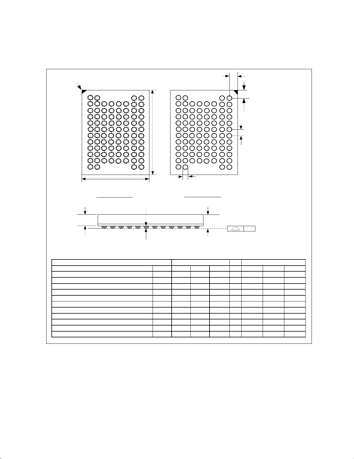
3.0 Package Information
The following two packages are offered with the 32WQ and 64WQ Family.
Figure 2: Mechanical Specifications for 1- or 2-Die SCSP Device (8x10x1.2 mm)
A1 Index
Mark
A
B
C
D
E
F
G
H
J
K
L
M
123 456 78
E
Top View - Ball
Down
A2
S1
2345678
1
A
B
C
D
E
F
D
G
H
J
K
L
M
b
Bottom View - Ball Up
A1
A
S2
e
Y
Drawi ng not to scale.
Millimeters Inches
Di me n s i on s S ymbol Mi n Nom Ma x No t e s Mi n No m Max
Package Heigh t A 1.200 0.0472
Ball Heig h t A1 0.200 0.0079
Package Body Thickne s s A2 0.860 0.0339
Ball (Lead) W idth b 0.325 0.375 0.425 0.0128 0.0148 0.0167
Package Body Len gth D 9.900 10.000 10.100 0.3898 0.3937 0.3976
Package Body W id th E 7.900 8.000 8.100 0.3110 0.3150 0.3189
Pitch e 0.800 0.0315
Ball (Lea d) Co u nt N 88 88
Seating Plane Coplanarity Y 0.100 0.0039
Corner t o Ball A1 Dis tan ce Along E S1 1.100 1.200 1.300 0.0433 0.0472 0.0512
Corner t o Ball A1 Dis tan ce Along D S2 0.500 0.600 0.700 0.0197 0.0236 0.0276
Datasheet November 2007
10 Order Number: 251407-13
Page 11
32WQ and 64WQ Family with Asynchronous RAM
Figure 3: Mechanical Specifications for Triple-Die SCSP Device (8x10x1.4 mm)
A1
Ind ex
Mark
12345678
A
B
C
D
E
F
G
H
J
K
L
M
E
Top View - Ball Down Bo tt om View - Ball Up
A2
S1
12345678
A
B
C
D
E
F
D
G
H
J
K
L
M
b
A1
A
S2
e
Y
Drawing not to scale.
Millimeters Inches
Dimens i ons Symbol Min Nom Max Notes Min Nom Max
Pac kage Heigh t A 1.400 0.0551
Ball Heigh t A 1 0.200 0.0079
Package Body Thickness A2 1.070 0.0421
Ball (Lea d) W idth b 0.325 0.375 0.425 0.0128 0.0148 0.0167
Package Body Length D 9.900 10.000 10.100 0.3898 0.3937 0.3976
Package Body Width E 7.900 8.000 8.100 0.3110 0.3150 0.3189
Pitc h e 0.800 0.0315
Ball (Lead) Count N 88 88
Sea ting Plane Cop lan arity Y 0.100 0.0039
Corner to Ball A1 Distance Along E S1 1.100 1.200 1.300 0.0433 0.0472 0.0512
Corner to Ball A1 Distance Along D S2 0.500 0.600 0.700 0.0197 0.0236 0.0276
November 2007 Datasheet
Order Number: 251407-13 11
Page 12
32WQ and 64WQ Family with Asynchronous RAM
32WQ and 64WQ Family with Asynchronous RAM
Table 1: 64-Mbit Flash + 32-Mbit Flash Die W18/W30 SCSP Memory Map and Partitioning
Block Size
(KW)
4 63-70 1F8000-1FFFFF
32 56-62 1C0000-1F7FFF
32 8-14 008000-03FFFF
4 0-7 000000-007FFF
Block # Address Range
Flash Die #2
(32-Mbit) To p
Parameter
Flash Die #1
(64-Mbit)
Bottom
Parameter
Partitioning
Parameter
Partition
Main Partitions
Main Partitions
Parameter
Partition
Partition 0
Partition 1 32 48-55 180000-1BFFFF
Partition 2 32 40-47 140000-17FFFF
Partition 3 32 32-39 100000-13FFFF
Partitions 4-7 32 0-31 000000-0FFFFF
Partitions 8-15 32 71-134 200000-3FFFFF
Partitions 4-7 32 39-70 100000-1FFFFF
Partition 3 32 31-38 0C0000-0FFFFF
Partition 2 32 23-30 080000-0BFFFF
Partition 1 32 15-22 040000-07FFFF
Partition 0
Table 2: 64-Mbit Dual-Flash Die W18/W30 SCSP Memory Map and Partitioning
Partitioning
Block Size
(KW)
Block # Address Range
Parameter
Partition
Flash Die #2
(64-Mbit) Top
Parameter
Flash Die #1
(64-Mbit)
Bottom
Parameter
Datasheet November 2007
12 Order Number: 251407-13
Main Partitions
Main Partitions
Parameter
Partition
Partition 0
Partition 1 32 112-119 380000-3BFFFF
Partition 2 32 104-111 340000-37FFFF
Partition 3 32 96-103 300000-33FFFF
Partitions 4-7 32 64-95 200000-2FFFFF
Partitions 8-15 32 0-63 000000-1FFFFF
Partitions 8-15 32 71-134 200000-3FFFFF
Partitions 4-7 32 39-70 100000-1FFFFF
Partition 3 32 31-38 0C0000-0FFFFF
Partition 2 32 23-30 080000-0BFFFF
Partition 1 32 15-22 040000-07FFFF
Partition 0
4 127-134 3F8000-3FFFFF
32 120-126 3C0000-3F7FFF
32 8-14 008000-03FFFF
4 0-7 000000-007FFF
Page 13
32WQ and 64WQ Family with Asynchronous RAM
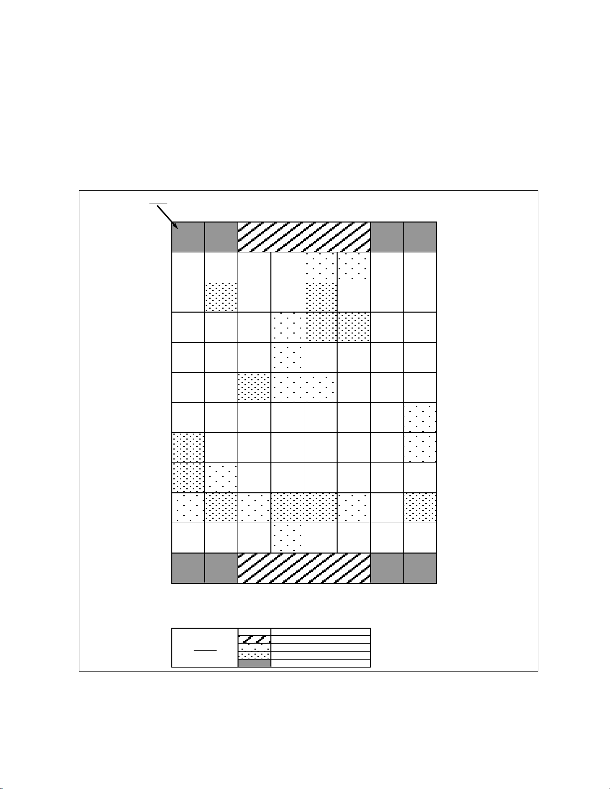
4.0 Ballout and Signal Description
4.1 Signal Ballout
Figure 4 shows the 32WQ and 64WQ W18/W30 SCSP family 88-ball (8x10 active ball
matrix) device.
Figure 4: 88-Ball (8x10 Active Ball Matrix) QUAD+ Ballout
Pin 1
12345678
A DU DU DU DU A
B A4 A18 A19 VSS F1-VCC F2-VCC A21 A11 B
C A5 R-LB# A23 VSS S-CS2 CLK A22 A12 C
D A3 A17 A24 F- VPP R-WE# P 1-C S# A9 A13 D
E A2 A7 A25 F-WP# ADV# A20 A10 A15 E
F A1 A6 R-UB# F-RST# F-WE# A8 A14 A16 F
G A0 DQ8 DQ2 DQ10 DQ5 DQ13 WAIT F2-CE# G
R-OE# DQ0 DQ1 DQ3 DQ12 DQ14 DQ7 F2-OE#
H
S-CS1# F1-OE# DQ9 DQ11 DQ4 DQ6 DQ15 VCCQ
J
H
J
F1-CE# P2-CS# F3-CE# S-VCC P-VCC F2-VCC VCCQ
K
VSS VSS VCCQ F1-VCC VSS VSS VSS VSS
L
DU DU DU DU
M
12345678
P-Mode/
P-CRE
K
L
M
Top View - Ball Side Down
Global Signals
Legend:
November 2007 Datasheet
Order Number: 251407-13 13
De-Populated Balls
Flash Specific
SRAM/PSRAM Specific
Do Not Use
Page 14

32WQ and 64WQ Family with Asynchronous RAM
32WQ and 64WQ Family with Asynchronous RAM
4.2 Signal Descriptions
Table 3: Signal Descriptions (Sheet 1 of 2)
Symbol Type Name and Function
ADDRESS INPUTS: Inputs for all die addresses during read and write operations. Addresses are
internally latched during write operations.
• 4-Mbit: A[17:0]
• 8-Mbit: A[18:0]
A[21:0] Input
D[15:0]
CLK Input
ADV# Input
WAIT Output
F[3:1]-CE# Input
S-CS1#
S-CS2
P[2:1]-CS# Input
F[2:1]-OE# Input
R-OE# I np ut
Input/
Output
Input
• 16-Mbit: A[19:0]
• 32-Mbit: A[20:0]
• 64-Mbit: A[21:0]
A0 is the lowest-order word address.
A[25:22] denote high-order addresses reserved for future device densities
DATA INPUTS/OUTPUTS: Inputs data and commands during write cycles; outputs data during read
cycles. Data signals float when the device or its outputs are deselected. Data are internally latched
during writes.
FLASH CLOCK: CLK synchronizes the selected flash die to the memory bus frequency in
synchronous-read mode. During synchronous read operations, the initial address is latched on the
rising edge of ADV#, or the rising/ falling edge of CLK when ADV# is low, whichever occurs first.
CLK is only used in synchronous-read mode. Refer to the flash discrete product datasheet for
information on how to use this signal in asynchronous-read mode.
FLASH ADDRESS VALID: Low-true; During synchronous read operations, the initial address is
latched on the rising edge of ADV#, or the rising/ falling edge of CLK when ADV# is low, whichever
occurs first.
Refer to the flash discrete product datasheet for information on how to use this signal in
asynchronous-read mode.
FLASH WAIT: When asserted, WAIT indicates invalid data from the selected flash die on D[15:0].
WAIT is High-Z whenever the flash die is deselected (CE# = V
WAIT is only used in synchronous array-read mode. Refer to the flash discrete product datasheet for
information on how to use this signal in asynchronous-read mode.
FLASH CHIP ENABLE: Low-true; CE#-low selects the associated flash memory die. When asserted,
flash internal control logic, input buffers, decoders, and sense amplifiers are active. When deasserted,
the associated flash die is deselected; power is reduced to standby levels, data and WAIT outputs are
placed in High-Z.
F1-CE# selects flash die #1; F2-CE# selects flash die #2 and is RFU on combinations with only one
flash die. F3-CE# selects flash die #3 and is RFU on SCSP combinations with only one or two flash
die.
SRAM CHIP SELECTS: When both SRAM chip selects are asserted, SRAM internal control logic, input
buffers, decoders, and sense amplifiers are active. When either/both SRAM chip selects are
deasserted (S-CS1# = V
standby levels.
S-CS1# and S-CS2 are only available on SCSP combinations with SRAM die.
PSRAM CHIP SELECTS: Low-true; When asserted, PSRAM internal control logic, input buffers,
decoders, and sense amplifiers are active. When deasserted, the PSRAM is deselected and its power
is reduced to standby levels.
P1-CS# selects PSRAM die #1 and is available only on SCSP combinations with PSRAM die. This ball is
RFU on SCSP combinations without PSRAM. P2-CS# selects PSRAM die #2 and is available only on
SCSP combinations with two PSRAM die. This ball is RFU on SCSP combinations without PSRAM or
with a single PSRAM.
FLASH OUTPUT ENABLE: Low-true; OE#-low enables the flash output buffers. OE#-high disables
the flash output buffers, and places the flash outputs in High-Z.
F1-OE# controls the outputs of flash die #1; F2-OE# controls the outputs of flash die #2 and #3, and
is available only on SCSP combinations with two or three flash die and is RFU on SCSP combinations
with only one flash die.
RAM OUTPUT ENABLE: Low-true; R-OE#-low enables the RAM output buffers. R-OE#-high disables
the RAM output buffers, and places the RAM outputs in High-Z.
R-OE# is only available on SCSP combinations with RAM die.
and/or S-CS2 = VIL), the SRAM is deselected and its power is reduced to
IH
). WAIT is not gated by OE#.
IL
Datasheet November 2007
14 Order Number: 251407-13
Page 15

32WQ and 64WQ Family with Asynchronous RAM
Table 3: Signal Descriptions (Sheet 2 of 2)
Symbol Type Name and Function
R-UB#
R-LB#
Input
F-WE# Input
R-WE# Input
F-WP# Input
F-RST# Input
F-VPP
F-VPEN
Power
P-MODE Input
F[2:1]-VCC Power
S-VCC Power
P-VCC Power
VCCQ Power FLASH OUTPUT-BUFFER POWER: Supplies power for the I/O output buffers.
VSS Power Grou nd: Connect to ground. Do not float any VSS connection.
RFU — Reserved for Future Use: Reserve for future device functionality/ enhancements.
DU — Don’t Use: Do not connect to any other signal, or power supply; must be left floating.
RAM UPPER/ LOWER BYTE ENABLES: Low-true; During RAM reads, R-UB#-low enables the RAM
high-order bytes on D[15:8], and R-LB#-low enables the RAM low-order bytes on D[7:0].
R-UB# and R-LB# are only available on SCSP combinations with either SRAM die or PSRAM die.
FLASH WRITE ENABLE: Low-true; WE# controls writes to the selected flash die. Address and data
are latched on the rising edge of WE#.
RAM WRITE ENABLE: Low-true; R-WE# controls writes to the RAM die.
R-WE# is only available on SCSP combinations with RAM die.
FLASH WRITE PROTECT: Low-true; WP# enables/disables the lock-down protection mechanism of
the flash die. WP#-low enables the lock-down mechanism- locked down blocks cannot be unlocked
with software commands. WP#-high disables the lock-down mechanism, allowing locked down blocks
to be unlocked with software commands.
FLASH RESET: Low-true; RST#-low initializes flash internal circuitry and disables flash operations.
RST#-high enables flash operation. Exit from reset places the flash in asynchronous read array mode.
FLASH PROGRAM/ ERASE POWER: A valid F-V
operations. Flash memory array contents cannot be altered when F-V
program operations at invalid F-V
discrete product datasheet for additional details.
(Erase/Program/Block Lock Enables) is not available for W18/W30 products.
F-V
PEN
) voltages should not be attempted. Refer to the flash
PP(VPEN
voltage on this ball enables flash program/erase
PP
PP(VPEN
PSRAM MODE: Low-true; P-MODE is used to enter/exit low power mode.
Low power mode is not applicable to 38F2020W0ZTQ1, 38F2020W0ZBQ1, 38F2030W0YTQ1,
38F2030W0YBQ1, 38F2030W0ZTQ2, 38F2030W0ZBQ2, 38F1030W0ZTQ0, 38F1030W0ZBQ0.
P-Mode is only available on SCSP combinations with PSRAM die.
FLASH LOGIC POWER: F1-VCC supplies power to the core logic of flash die #1; F2-VCC supplies
power to the core logic of flash die #2 and #3. Write operations are inhibited when F-V
Device operations at invalid F-V
voltages should not be attem pted.
CC
F2-VCC is only available on SCSP combinations with two or three flash die, and is RFU on SCSP
combinations wi th only one flash die.
SRAM Power Supply: Supplies power to the SRAM die.
S-VCC is only available on SCSP combinations with SRAM die.
PSRAM Power Supply: Supplies power to the PSRAM die.
P-VCC is only available on SCSP combinations with PSRAM die.
) < V
PPLK(VPENLK
< V
CC
). Erase/
.
LKO
November 2007 Datasheet
Order Number: 251407-13 15
Page 16

32WQ and 64WQ Family with Asynchronous RAM
32WQ and 64WQ Family with Asynchronous RAM
5.0 Maximum Ratings and Operating Conditions
5.1 Absolute Maximum Ratings
Warning: Stressing the device beyond the “Absolute Maximum Ratings” may cause permanent
damage. These are stress ratings only.
NOTICE: This document contains inform ation available at the time of its release. The specifications
are subject to change without notice. Verify with your local Numonyx sales office that you have the
latest datasheet before finalizing a design.
Table 4: Absolute Maximum Ratings
Parameter Min Max Unit Notes
Temperature under Bias Extended –25 +85 °C 7
Storage Temperature –55 +125 °C
Voltage On Any Signal (exce pt F[2:1]-V
and P-V
CC)
F[2:1]-V
V
CCQ
F-V
I
SH
Notes:
1. 90 nm is only avail with the 1.8 V I/O.
2. All Specified voltages are relative to V
3. All Specified voltages are relative to V
4. Maximum DC voltage on F-VPP may overshoot to +14.0 V for periods < 20 ns.
5. F-V
6. Output shorted for no more than one second. No more than one output shorted at a time.
7. Devices available with -30
Vol tag e –0.5 +2.45 V 2,3
CC
, S-V
and P-VCC Voltage
CC
Vol tag e –0.2 +14.0 V 2,3,4,5
PP
Output Short Circuit Current – 100 mA 6
and F-VPP signals. For 90 nm devices, during transitions, this level may overshoot to –1.5 V for periods < 20 ns, during
transitions, may overshoot to F-V
and F-VPP signals. For 130 nm devices, during transitions, this level may overshoot to –2 V for periods < 20 ns, during
transitions, may overshoot to F-V
program voltage is normally V
PP
ns. F-V
38F2030W0YBQ1, 38F2030W0ZTQ2, 38F2030W0ZBQ2, 38F1030W0ZTQ0, 38F1030W0ZBQ0, 38F2030W0YTQF,
38F2030W0YBQF, 38F2040W0YTQF, 38F2040W0YBQF
can be V
PP
for 1000 erase cycles on main blocks, 2500 cycles on parameter blocks.
PPH
, V
F-V
CC
CCQ,
+ 1.5 V for periods < 20 ns.
CC
+ 2 V for pe riods < 20 n s.
CC
PPL
o
C temperature specifications are: 38F2020W0ZTQ1, 38F2020W0ZBQ1, 38F2030W0YTQ1,
S-VCC
PP,
. Minimum DC voltage is –0.2 V on input/output signals, –0.2 V on F[2:1]-VCC
SS
. Minimum DC voltage is –0.2 V on input/output signals, –0.2 V on F[2:1]-VCC
SS
. The maximum DC voltage on F-VPP may overshoot to +14 V for periods < 20
1.8 V I/O –0.2 +2.45 V 1,2,3
3.0 V I/O –0.2 +3.6 V 2,3
1.8 V I/O –0.2 +2.45 V 1,2,3
3.0 V I/O –0.2 +3.6 V 2,3
5.2 Operating Conditions
Warning: Operation beyond the “Operating Conditions” is not recommended and extended
Table 5: Operating Conditions (Sheet 1 of 2)
Symbol Parameter
T
C
F-V
CC
Datasheet November 2007
16 Order Number: 251407-13
exposure beyond the “Operating Conditions” may affect device reliability.
Flash +
Flash
Min Max Min Max Min Max
Operating Temperature –25 +85 –25 +85 –25 +85 °C 2
Flash Supply Voltage 1.7 1.95 1.7 1.95 1.7 1.95 V
Flash +
SRAM
Flash +
PSRAM
Unit Notes
Page 17

32WQ and 64WQ Family with Asynchronous RAM
Table 5: Operating Conditions (Sheet 2 of 2)
V
CCQ
S-V
P-V
V
V
Note:
1. F-V
2. Devices available with -30
Flash I/O Voltage
CC
PSRAM and SRAM Supply Voltage
CC
Flash Program Logic Level 0.9 1.95 0.9 1.95 0.9 1.95 V
PPL
Flash Factory Program Voltage 11.4 12.6 11.4 12.6 11.4 12.6 V 1
PPH
is normally V
PP
temperatures and 2500 cycles on parameter blocks at extended temperature.
38F2030W0YBQ1, 38F2030W0ZTQ2, 38F2030W0ZBQ2, 38F1030W0ZTQ0, 38F1030W0ZBQ0, 38F2030W0YTQF,
38F2030W0YBQF, 38F2040W0YTQF, 38F2040W0YBQF
. F-VPP can be connected to 11.4 V–12.6 V for 1000 cycles on main blocks for extended
PPL
o
C temperature specifications are: 38F2020W0ZTQ1, 38F2020W0ZBQ1, 38F2030W0YTQ1,
3.0 V I/O 2.2 3.3 2.2 3.3 2.7 3.1 V
1.8 V I/O 1.7 1.95 1.7 1.95 1.8 1.95 V
5.3 Capacitance
NOTICE: Refer to the Numonyx™ Wireless Flash Memory (W18) Datasheet
(order number 290701) and Numonyx™ Wireless Flash Memory (W30)
Datasheet (order number 290702) for flash capacitance details. For SCSP
products with two flash die, flash capacitances for each of the flash die need
to be considered accordingly.
Table 6: SRAM, PSRAM Capacitance
Symbol Parameter Typ Unit Cond ition
Input Capacitance 10 pF VIN = 0.0 V, Tc = 25 °C, f = 1 MHz
Output Capacitance 10 pF V
= 0.0 V, Tc = 25 °C, f = 1 MHz
OUT
C
C
OUT
IN
November 2007 Datasheet
Order Number: 251407-13 17
Page 18

6.0 Electrical Specifications
6.1 DC Characteristics
SRAM and PSRAM DC characteristics are shown in Tab l e 7 and Tab l e 8 . Refer to the
Numonyx Wireless Flash Memory (W18) Datasheet (order number 290701) and the
Numonyx Wireless Flash Memory (W30) Datasheet (order number 290702) for flash DC
characteristics.
Table 7: SRAM DC Characteristics
32WQ and 64WQ Family with Asynchronous RAM
32WQ and 64WQ Family with Asynchronous RAM
Parameter Description Test Conditions
1.8 V SRAM 3.0 V SRAM
Min Max Min Max
S-V
V
DR
Voltage Range 1.7 1.95 2.2 3.3 V
CC
VCC for Data Retention 1.0 – 1.5 – V
4M–25–45
I
CC
Operating Current at
min cycle time
= 0 mA
I
IO
16M – 40 – 55
4M – 4 – 10
I
CC2
Operating Current at
max cycle time (1 μs)
= 0 mA
I
IO
16M – 10 – 15
S-CS1# ≥ S-V
I
SB
Standby Current
or S-CS2 ≤ V
Address/Data toggling at
minimum cycle time
1.8 V SRAM:
I
DR
V
OH
V
OL
V
IH
V
IL
I
OH
I
OL
*I
IL
*I
LDR
Current in Data
Retention m ode
Output HIGH Voltage I
Output LOW Voltage
Input HIGH Voltage
Input LOW Voltage -0.2 0.4 -0.2 0.6 V
Output HIGH Current – – – – mA
Output LOW Current – – – – mA
Input Leakage Current -0.2 < VIN < S-V
Input Leakage Current
in Data Retention Mod e
S-V
CC
3.0 V SRAM:
S-V
CC
-0.2 < V
CC
SS
= 1.0 V
= 1.5 V
= -100 μA
OH
= 100 μA,
I
OL
V
CCMIN
< S-V
IN
S-V
CC
-0.2V
4M–12–15
+0.2V
16M – 30 – 45
4M–6–5
8M–10–12
16M – 18 – 15
S-V
0.15
-
CC
–
S-V
0.1
-
CC
-0.1 0.2 -0.1 0.1 V
-
S-V
0.4
+ 0.2 V -1 +1 -1 +1 μA
CC
+ 0.2 V
CC
= V
DR
S-VCC+
CC
0.2
-1 +1 -1 +1 μA
S-VCC -
0.4
S-VCC+
0.2
* Input leakage currents include Hi-Z output leakage for bi-directional buffers with tri-state
outputs.
Unit
mA8M–35–50
mA8M – 6 – 10
μA8M–20–25
μA
–V
V
Datasheet November 2007
18 Order Number: 251407-13
Page 19

32WQ and 64WQ Family with Asynchronous RAM
Table 8: PSRAM DC Characteristics
Parameter Description Test Conditions
1.8 V PSRAM 3.0 V PSRAM
Min Max Min Max
V
CC
Voltage Range 1.8 1.95 2.7 3.1 V
8M – – – 30
I
CC
Operating Current
at min cycle time
I
IO
= 0 mA
16M – 30 – 35
16M – 20 – – mA 3
32M – 35 – 45 mA 2
8M – – – 5
32M – – – 7
-
8M – – – 80
16M – 100 – 100
-
16M – – – 85
-
CC
32M – 100 – 100
16M – – – 10
32M – 30 – 10
0.8P V
CC
–2.4–V4
P-V
CC
CCMin
-0.1 0.2 -0.1 0.3 V 5
P-V
+
0.8P -V
CC
-
P-V
CC
0.3
–0.3 0.2P - V
P-V
CC
0.3
CC
0.2
P-V
+
CC
–0.2 0.4 -0.2 0.6 V 5
+ 0.2
CC
CC
DR
+ 0.2
-1 +1 -1 +1 μA1, 2
-1 +1 -1 +1 μA1, 2
-
0.3
CC
–V5
–0.4V4
-
P-V
CC
0.3
P-VCC-
0.4
P-V
0.2
0.2
CC
CC
-0.2 0.5 V 4
I
I
V
I
V
V
V
I
I
CC2
SB
sbd
OH
OL
IH
IL
IL
OL
Operating Current
at max cycle time
(1 μs)
Standby Current
Deep PowerDown
Output HIGH
Volt age
Output LOW
Volt age
Input HIGH
Volt age
Input LOW
Volt age
Input Leakage
Current
Output Leakage
Current
= 0 mA
I
IO
P-CS# ≥ P-V
0.2V.
CC
All inputs stable
(either high or
low)
P-CS# ≥ P-V
P-Mode ≥ P-V
Address/Data
toggling at
minimum cycle
0.2V or
0.2V
time
CC
P-Mode ≤ 0.2 V
I
= -0.5 mA
OH
= -0.1 mA 1.4 –
I
OH
= 1 mA, – 0.2P - V
I
OL
= 0.1 mA, V
I
OL
-0.2 < VIN < P-V
V
-0.2 < V
P-V
< P-V
IN
CC
V
= V
Notes:
1. Input Leakage currents include Hi-Z output leakage for bi-directional buffers with tri-state outputs.
2. All currents are in RMS unless noted otherwise.
3. Applicable only to parts 38F1030W0YxQF & 38F2030W0YxQF.
4. Applicable to parts with P-Mode pin (38F2030W0ZxQ1, 38F2040W0YxQ0, 28F2240WWYxQ0).
5. Applicable to No-P-Mode (38F1030W0YxQF, 38F1030W0YxQ2, 38F1030W0ZxQ0, 38F2030W0YxQ1,
38F2030W0YxQF, 38F2030W0YxQ2, 38F2030W0YxQF, 38F2030W0ZxQ2, 38F2040W0ZxQ0).
Unit Notes
mA 2
mA 216M – 5 – 7
μA2, 4
μA2, 5
μA2, 4
+
V4
+
V5
November 2007 Datasheet
Order Number: 251407-13 19
Page 20

7.0 AC Characteristics
7.1 Flash AC Characteristics
Refer to the Numonyx Wireless Flash Memory (W18) Datasheet (order number 290701)
and Numonyx Wireless Flash Memory (W30) Datasheet (order number 290702)
7.2 SRAM AC Characteristics
Table 9: SRAM AC Characteristics
32WQ and 64WQ Family with Asynchronous RAM
32WQ and 64WQ Family with Asynchronous RAM
RC
AA
CO1
CO2
OE
BA
LZ
OLZ
HZ
OHZ
OH
BLZ
BHZ
1
Read Cycle Time 70 – ns 1
Address to Output Delay – 70 ns 1
S-CS1# to Output Delay – 70 ns 1
S-CS2 to Output Delay – 70 ns 1
R-OE# to Output Delay – 35 ns 1
R-UB#, R-LB# to Output Delay – 70 ns 1
S-CS1# or S-CS2 to Output in Low-Z 5 – ns 1,3,4
R-OE# to Output in Low-Z 0 – ns 1,4
S-CS1# or S-CS2 to Output in High-Z 0 25 ns 1,2,3,4
R-OE# to Output in High-Z 0 25 ns 1,2,4
Output Hold (from Address, S-CS1#, S-CS2 or R-OE# Change,
whichever occurs first)
R-UB#, R-LB# to Output in Low-Z 0 – ns 1,4
R-UB#, R-LB# to Output in High-Z 0 25 ns 1,4
Parameter Min Max Unit Notes
Figure 5, “AC Waveform SRAM Read Operations” .
HZ
and t
are defined as the time at which the outputs achieve the open circuit conditions and are not
OHZ
#Symbol
R1 t
R2 t
R3 t
R3 t
R4 t
R5 t
R6 t
R7 t
R8 t
R9 t
R10 t
R11 t
R12 t
Note:
1. See
2. Timings of t
3. At any given temperature and voltage condition, t
referenced to output voltage levels.
to device interconnection.
4. Sampled, but not 100% tested.
(Max) is less than t
HZ
0–ns 1
(Max) both for a given device and from device
LZ
Datasheet November 2007
20 Order Number: 251407-13
Page 21

32WQ and 64WQ Family with Asynchronous RAM
Figure 5: AC Waveform SRAM Read Operations
ADDRESSES
S-CS1#
S-CS2
R-OE#
R-WE#
DAT A
R-UB#, R-LB #
Standby
R6
R2
R11
R5
R1R1
Address Stable
R8R3
R9R7
R4
R10
Valid Data
R12
November 2007 Datasheet
Order Number: 251407-13 21
Page 22

Table 10: SRAM AC Characteristics (Write)
32WQ and 64WQ Family with Asynchronous RAM
32WQ and 64WQ Family with Asynchronous RAM
#Symbol
W1 t
W2 t
W3 t
W4 t
W5 t
W6 t
W7 t
W8 t
W9 t
Notes:
1. See
2. A write occurs during the overlap (t
3. t
4. t
5. t
WE# goes low with asserting R-UB# and R-LB# for single byte operation or simultaneously asserting R-UB#R-LB# and
R-LB# for double byte operation. A write ends at the earliest high transition of S-CS1# and R-WE#.
WP
AS
WR
goes high.
1
WC
WP
DW
AW
CW
DH
WR
BW
Write Cycle Time 70 – ns 1
Address Setup to R-WE# (S-CS1#) and R-UB#/R-LB# Low 0 – ns 1,4
AS
R-WE# (S-CS1#) Pulse Width 55 – ns 1,2,3
Data to Write Time Overlap 30 – ns 1
Address Setup to R-WE# (S-CS 1#) High 60 – ns 1
S-CS1# (R-WE#) S etup to R-WE# (S-CS1#) High 60 – ns 1
Data Hold from R-WE# (S-CS1#) High 0 – ns 1
Write Re covery 0 – ns 1,5
R-UB#, R-LB# Setup to R-WE# (S-CS1#) High 60 – ns 1
Figure 6, “AC Waveform SRAM Write Operations” .
is measured from S-CS1# low to the end of a write.
is measured from the address valid to the beginning of a write.
Parameter Min Max Unit Notes
) of low S-CS1# and low R-WE#. A write begins when S-CS1# goes low and R-
WP
is measured from the end of write to the address chang e. t
Figure 6: AC Waveform SRAM Write Operations
ADDRESSES
Standby
S-CS1#
Address Stable
applied in case a write ends as S-CS1# or R-WE#
WR
W1W1
W8W6
S-CS2
R-OE#
W3W3
W5
R-WE#
W7W4
DAT A
Data In
W9W9W2
R-UB#, R-LB #
7.3 PSRAM AC Characteristics
Table 11: PSRAM AC Characteristics (85ns or 88ns Initial Access) — Read Operations
# Symbol Parameter
R1 t
R2 t
R3 t
Read Cycle Time 88 4,000 85 4,000 ns
RC
Address to Output Delay –88–85ns
AA
P-CS# to Output Delay –88–85ns
CO
5
1.8 V 3.0 V
Unit Notes
MinMaxMinMax
Datasheet November 2007
22 Order Number: 251407-13
Page 23

32WQ and 64WQ Family with Asynchronous RAM
Table 11: PSRAM AC Characteristics (85ns or 88ns Initial Access) — Read Operations
# Symbol Parameter
5
1.8 V 3.0 V
Unit Notes
Min Max Min Max
R4 t
R5 t
R6 t
R7 t
R8 t
R9 t
R10 t
R11 t
R12 t
PR1 t
PR2 t
OLZ
OHZ
BLZ
BHZ
R-OE# to Output Delay – 65 – 40 ns
OE
R-UB#, R-LB# to Output Delay – 88 – 85 ns
BA
P-CS# to Output in Low-Z 10 – 10 – ns 1,2
LZ
R-OE# to Output in Low-Z 5 – 0 – ns 2
P-CS# to Output in High-Z – 25 0 25 ns 1,2,3
HZ
R-OE# to Output in High-Z – 25 0 25 ns 2,3
Output Hold (from Address, P-CS# or R-
OH
OE# change, whichever occurs first)
5–0–ns
R-UB#, R-LB# to Output in Low-Z 5 – 0 – ns 2
R-UB#, R-LB# to Output in High-Z – 25 0 25 ns 2
Page Cycle Time 30 – 40 – ns 4
PC
Page Access Time – 30 – 35 ns 4
PA
Note:
1. At any given temperature and voltage condition, t
2. Sampled but not 100% tested.
3. Timings of t
4. 4-Word Page read only available for 32-Mbit PSRAM. No page mode feature for 16-Mbit PSRAM.
5. Applicable to parts with 85ns or 88ns initial access time: 38F2030W0ZxQ1, 38F2040W0YxQ0, 38F2040W0ZxQ0,
to device interconnection.
and t
referenced to output voltage levels.
HZ
are defined as the time at which the outputs achieve the open circuit conditions and are not
OHZ
(Max) is less than tLZ (Max) both for a given device and from device
HZ
28F2240WWYxQ0.
November 2007 Datasheet
Order Number: 251407-13 23
Page 24

32WQ and 64WQ Family with Asynchronous RAM
32WQ and 64WQ Family with Asynchronous RAM
Table 12: PSRAM AC Characteristics (70ns Initial Access) — Read Operations
#Symbol
1
Parameter
7
1.8 V 3.0 V
Unit Notes
Min Max Min Max
R1 t
R2 t
R3 t
R4 t
R5 t
R6 t
R7 t
R8 t
R9 t
R10 t
R11 t
R12 t
PR1 t
PR2 t
OLZ
OHZ
BLZ
BHZ
t
CEL
Read Cycle Time
RC
Address to Output Delay –70–70ns
AA
P-CS# to Output Delay –70–70ns
CO
R-OE# to Output Delay –45–45ns
OE
R-UB#, R-LB# to Output Delay – 70 – 70 ns
BA
P-CS# to Output in Low-Z 5 – 5 – ns 3
LZ
R-OE# to Output in Low-Z 0 – 0 – ns
P-CS# to Output in High-Z 025025ns3, 4
HZ
R-OE# to Output in High-Z 0 25 0 25 ns 4
Output Hold (from Address, P-CS# or R-OE#
OH
change, whichever occurs first)
R-UB#, R-LB# to Output in Low-Z 0 – 0 – ns
R-UB#, R-LB# to Output in High-Z 0 25 0 25 ns
Page Cycle Time 25 – 25 – ns 5
PC
Page Access Time – 25 – 25 ns 5
PA
CE# low-time restriction – 8,000 ns 4 ns 6
70 15000 70 15000
70 8000 – – 2
ns
0–0–ns
Note:
1. See
2. Spec’s only applicable to parts 38F1030W0YxQF & 38F2030W0YxQF
3. At any given temperature and voltage condition, t
4. T imings of t
5. 4-Word Page read only available for 16-Mbit PSRAM. No page mode feature for 8-Mbit PSRAM. Parts 38F1030W0YxQF &
6. CE# must go high and be maintained high for a minimum of 10ns at least once every 8,000ns
7. Applicable to 70ns initial access P-SRAM’s ( 38F1030W0YxQ2, 38F1030W0ZxQ0, 38F2030W0YxQ1, 38F2030W0YxQ2,
Figure 7, “AC Waveform of PSRAM Read Operations” on page 25 and Figure 8, “AC
Waveform of PSRAM 4-Word Page Read Operation” on page 25
to device interconnection.
referenced to output voltage levels.
HZ
and t
are defined as the time at which the outputs achieve the open circuit conditions and are not
OHZ
(Max) is less than t
HZ
(Max) both for a given device and from device
LZ
38F2030W0YxQF do not support page mode, so this spec will not apply to them
38F2030W0YxQF, 38F2030W0ZxQ2)
Datasheet November 2007
24 Order Number: 251407-13
Page 25

32WQ and 64WQ Family with Asynchronous RAM
s
s
s
A
Figure 7: AC Waveform of PSRAM Read Operations
R1R2R1
ADDRESSES
P-CS#
R-UB#, R-L B #
R-OE#
R7
R11
DAT A
R8R3
R12R5
R9R4
R10R6
Valid Data
Figure 8: AC Waveform of PSRAM 4-Word Page Read Operation
R1R2R1
[Max:2]
R-OE#
v
A[1:0]
P-CS#
DAT A
Valid Addres
R7
Valid Data Vali d Data Valid Data Valid Data
Note: Available only for 32-Mbit PSRAM and line items with 16-Mbit PSRAM (70 ns) 38F2030W0YTQ1,
38F2030W0YBQ1, 38F2030W0ZTQ2, 38F2030W0ZBQ2, 38F1030W0ZTQ0, 38F1030W0ZBQ0. Not
applicable to 8-Mbit PSRAM.
Valid Addres
PR1PR1
Valid AddressValid AddressValid Addres
R8R3
R9R4
PR2R6
Table 13: PSRAM AC Characteristics—Write (Sheet 1 of 2)
1.8 V 3.0 V
Unit Notes
Min Max Min Max
0– 0 –ns4
WC
AS
WP
DW
1
Write Cycle Time 70 8000 70 – ns
Address Setup to R-WE#
(P-CS#) and R-UB#, R-LB# going low
R-WE#(P-CS#) Pulse Width 55 – 55 – ns 2,3
Data to Write Time Overlap 35 – 35 – ns
Parameter
#Symbol
W1 t
W2 t
W3 t
W4 t
7
November 2007 Datasheet
Order Number: 251407-13 25
Page 26

32WQ and 64WQ Family with Asynchronous RAM
32WQ and 64WQ Family with Asynchronous RAM
Table 13: PSRAM AC Characteristics—Write (Sheet 2 of 2)
1.8 V 3.0 V
Min Max Min Max
60 – 60 – ns
60 – 60 – ns
0– 0 –ns
60 – 60 – ns
applied in case a write ends as P-CS# or R-WE#
WR
AW
CW
WR
BW
t
CEL
WPH
DH
1
Address Setup to R-WE#
(P-CS#) Going High
P-CS# (R-WE#) Setup to R-WE# (P-CS#)
Going High
Data Hold from R-WE#
(P-CS#) High
Write Recovery 0 – 0 – ns 5
R-UB# , R- LB# Se tup to R-WE# (P- CS# ) Going
High
P-CE# low-time restriction – 8,000 – – ns 7,8
Write High Pulse Width 10 – – – ns 8
Parameter
Figure 9, “AC Waveform PSRAM Write Operation” .
WP
is measured from the end of a write to the address change. t
#Symbol
W5 t
W6 t
W7 t
W8 t
W9 t
W10 t
Notes:
1. See
2. A write occurs during the overlap (t
3. t
4. t
5. t
6. W3 is 70 ns for continuous write operations over 50 times.
7. P-CE# must go high and be maintained high for a minimum of 10ns at least once every 8,000ns
8. Spec’s only applicable to parts 38F1030W0YxQF & 38F2030W0YxQF
9. Applicable to 38F2020W0ZTQ1, 38F2020W0ZBQ1, 38F2030W0YTQ1, 38F2030W0YBQ1, 38F2030W0ZTQ2,
goes low with asserting R-UB# or R-LB# for single byte operation or simultaneously asserting R-UB# and R-LB# for
double byte operation. A write ends at the earliest transition when P-CS# goes high and R-WE# goes high.
is measured from P-CS# going low to end of a write.
WP
is measured from the address valid to the beginning of a write.
AS
WR
going high.
38F2030W0ZBQ2, 38F1030W0ZTQ0, 38F1030W0ZBQ0.
7
) of low P-CS# and low R-WE#. A write begins when P-CS# goes low and R-WE#
Unit Notes
Figure 9: AC Waveform PSRAM Write Operation
ADDRESSES
P-CS#
R-UB#, R-L B #
R-WE#
DAT A
W1W2W1
W6
W9
W8
W3W3
W5
W7W4
Data In
Datasheet November 2007
26 Order Number: 251407-13
Page 27

32WQ and 64WQ Family with Asynchronous RAM
7.4 Device AC Test Conditions
Figure 10: Transient Input/Output Reference Waveform
V
, P-V
CCQ
CC
/2,
V
Input Output
P-V
CCQ
/2
CC
0 V
Test Points
V
CCQ
P-V
/2,
/2
CC
Note: AC test inputs are driven to V
/2. Input rise and fall time (10% to 90%) < 5 ns. Worse case speed occurs at VCC = V
P-V
CC
, P-VCC for logic “1” and 0.0 V for logic “0”. input/output timing begins/ends at V
CCQ
Figure 11: Transient Equivalent Testing Load Circuit
ZO = 50 Ohm s
I/O
Output
P-VCC/2 = V
Notes:
1. Test configuration component value for worst case specification conditions.
2. C
includes jig capacitance.
L
50
Ohms
CCQ
/2,
CCQ
= 30 pf
C
L
CCMin
.
/2
November 2007 Datasheet
Order Number: 251407-13 27
Page 28

8.0 Flash Power Consumption
Refer to the Numonyx Wireless Flash Memory (W18) Datasheet (order number 290701)
and Numonyx Wireless Flash Memory (W30) Datasheet (order number 290702) for
detailed information.
32WQ and 64WQ Family with Asynchronous RAM
32WQ and 64WQ Family with Asynchronous RAM
Datasheet November 2007
28 Order Number: 251407-13
Page 29

32WQ and 64WQ Family with Asynchronous RAM
9.0 Device Operation
9.1 Bus Operations
Bus operations for the W18/W30 SCSP family involve the following chip enable and
output enable signals, respectively:
• F1-CE# for Flash Die#1 and F2-CE# for Flash Die#2
• F1-OE# for Flash Die#1 and F2-OE# for Flash Die#2
All other control signals are shared between the two flash die. Tab le to Tab le 1 6
explain the bus operations of products across this SCSP family. Refer to the W18/W30
discrete datasheets (order numbers 290701 and 290702) for single flash die SCSP bus
operations.
Table 14: Flash-Only Bus Operations
Mode
F1-CE#
Device
Sync Array Read H L L H L X Active H X
All Async /
Sync Non-Array
Read
Write HLHLX
Output Disable H L H H X X Active X X
Flash Die#1
Standby HHXXX X High-Z X X
Reset L XXXX XHigh-Z X X
F-RST#
H L L H X X Asserted H X
F1-OE#
ADV#
F-WE#
F-VPP
V
PPL
or
V
PPH
WAIT
Asserted H X
F2-CE#
F2-OE#
D[15:0]
Flash
D
OUT
Flash
D
OUT
Flash
D
IN
Flash
High-Z
Flash
High-Z
Flash
High-Z
Notes
2, 3, 4
1, 3, 4,
5
3, 4, 6
4
4
4
November 2007 Datasheet
Order Number: 251407-13 29
Page 30

Table 14: Flash-Only Bus Operations
32WQ and 64WQ Family with Asynchronous RAM
32WQ and 64WQ Family with Asynchronous RAM
Mode
ADV#
F1-CE#
Device
F-RST#
F-WE#
F1-OE#
F-VPP
Sync Array Read H H X H L X Active L L
All Async /
Sync Non-Array
Read
Write H H X L X
Output Disable H X X H X X Active L H
Flash Die#2
H H X H X X Asserted L L
V
PPL
or
V
PPH
Standby HXXXX XHigh-Z H X
Reset LXXXX X High-Z X X
Notes:
1. For asynchronous read operation, both die may be simultaneously selected, but may not simultaneously drive the
memory bus. See
2. WAIT is only valid during synchronous flash reads. WAIT is driven if F-CE# is asserted. Refer to the W18 or W30
3. For either flash die, F[2:1]-OE# and F-WE# should never be asserted simultaneously. If done so on a particular
4. L means V
5. Flash CFI query and status register accesses use D[7:0] only, all other reads use D[15:0].
6. Refer to W18/W30 datasheet for valid D
selection overlap.
datasheet (order number 290701 and 29702) for further information regarding WAIT Signal.
flash die, F[2:1]-OE# will override F-WE#.
Section 10.0, “Flash Command Definitions” on page 33 for details regarding flash
while H m eans VIH. X can be VIL or VIH for inputs, V
IL
during flash writes.
IN
WAIT
F2-CE#
Asserted L H
, V
PPL
PPH
or V
for F-VPP.
PPLK
F2-OE#
D[15:0]
Flash
D
OUT
Flash
D
OUT
Flash
D
IN
Flash
High-Z
Flash
High-Z
Flash
High-Z
Notes
2, 3, 4
1, 3, 4,
5
3, 4, 6
4
4
4
Table 15: Flash + SRAM Bus Operations
Mode
F-RST#
F[2:1]-CE#
Device
F[2:1]-OE#
Sync
Array
Read
HLLHL X Active
All Async/
Sync Nonarray
Read
H L L H X X Asserted
Write H L H L L
Flash Die(#1 or #2)
Output
Disable
HLHHX X Active
Standby HHXXX XHigh-Z
Reset L XXXX XHigh-Z
ADV#
F-WE#
F-VPP
V
PPL
or
V
PPH
WAIT
Asserted
S-CS2
S-CS1#
R-OE#
SRAM must be in High-Z
Any SRAM mode allowed
1, 2,
3, 5
1, 2,
3, 5,
6
3, 7
5
5
5
Notes
R-WE#
R-LB#
R-UB#,
D[15:0]
Flash
D
OUT
Flash
D
OUT
Flash
D
IN
Flash
High-Z
Flash
High-Z
Flash
High-Z
Datasheet November 2007
30 Order Number: 251407-13
Page 31

32WQ and 64WQ Family with Asynchronous RAM
Table 15: Flash + SRAM Bus Operations
Mode
ADV#
F-RST#
Device
F[2:1]-CE#
F-WE#
F[2:1]-OE#
F-VPP
Read
Flash must be in High-Z
Write LHXLL
Output
Disable
SRAM
Standby
Data
Reten tion
Any flash mode allowed
WAIT
S-CS2
S-CS1#
R-OE#
LHLHL
LHHHX
HX
XL
XXX
Same as SRAM standby
R-LB#
R-WE#
R-UB#,
SRAM
D
OUT
SRAM
D
IN
SRAM
High-Z
SRAM
High-Z
SRAM
High-Z
Notes:
1. For asynchronous read operati on, all die may be simultaneously selecte d, but may not simultaneously drive the
2. WAIT is only valid during synchronous flash reads. WAIT is driven if F-CE# is asserted.
3. For flash die, F[2:1]-OE# and F-WE# should never be asserted simultaneously. If done so, F[2:1]-OE# will
4. For SRAM, R-OE# and R-WE# should never be asserted simultaneously.
5. X can be V
6. Flash CFI query and status register accesses use D[7:0] only, all other reads use D[15:0].
7. Refer to W18 and W30 datasheet for valid D
8. The SRAM is enabled and/or disabled with the logical function: S-CS1# OR S-CS2.
9. The SRAM can be placed into data retention mode by lowering S-VCC to the V
memory bus.
override F-WE#.
or VIH for inputs, V
IL
PPL
, V
PPH
or V
for F-VPP.
PPLK
during flash writes.
IN
limit when in standby mode.
DR
Table 16: Flash + PSRAM Bus Operations
D[15:0]
Notes
1, 4,
8, 2
4, 5,
8, 2
5, 2
5, 8,
2
9, 2
Mode
WAIT
Asserted
P-CS#
P-Mode
R-OE#
R-WE#
PSRAM must be in High-Z
Any PSRAM mode allowed
R-LB#
R-UB#,
D[15:0]
Flash
D
OUT
Flash
D
OUT
Flash
D
IN
Flash
High-Z
Flash
High-Z
Flash
High-Z
Notes
1, 2,
3, 4, 6
1, 2,
3, 4,
6, 7
3, 4,
6, 8
6
6
6
ADV#
Device
Sync
Array
F-RST#
F[2:1]-CE#
F-WE#
F[2:1]-OE#
HLLHL XActive
F-VPP
Read
All Async/
Sync Nonarray
Read
Write H L H L X
Output
Disable
Flash Die(#1 or #2)
H L L H X X Asserted
V
PPL
or
V
PPH
HLHHX XActive
Standby H H X X X X High-Z
Reset L XXXX XHigh-Z
November 2007 Datasheet
Order Number: 251407-13 31
Page 32

Table 16: Flash + PSRAM Bus Operations
32WQ and 64WQ Family with Asynchronous RAM
32WQ and 64WQ Family with Asynchronous RAM
Mode
ADV#
Device
F-RST#
F[2:1]-CE#
F-WE#
F[2:1]-OE#
F-VPP
Read
Flash#1 and #2 must be in High-Z
Write LHHLL
Output
Disable
PSRAM
Standby H H X X X
Deep
Power-
Any flash mode allowed
WAIT
P-CS#
P-Mode
R-OE#
LHLHL
L HHH X
HLXXX
R-UB#,
R-LB#
D[15:0]
R-WE#
PSRAM
D
OUT
PSRAM
D
IN
PSRAM
High-Z
PSRAM
High-Z
PSRAM
High-Z
Notes
1, 5, 2
5, 2
6, 2
6, 2
6, 9, 2
Down
Notes:
1. For asynchronous read operation, all die may be simultaneously selected, but may not simultaneously drive the memory
2. WAIT is only valid during synchronous flash reads. WAIT is driven if F-CE# is asserted.
3. F1-CE# for Flash Die#1, F2-CE# for Flash Die#2. F1-OE# is for Flash Die#1, F2-OE# for Flash Die#2.
4. For either flash die, F[2:1]-OE# and F-WE# should never be asserted simultaneously. If done so on a particular flash
5. For PSRAM, R-OE# and R-WE# should never be asserted simultaneously.
6. X can be V
7. Flash CFI query and status register accesses use D[7:0] only, all other reads use D[15:0].
8. Refer to W30/W18 datasheet for Valid D
9. Deep power-down is not applicable to 38F2020W0ZTQ1, 38F2020W0ZBQ1, 38F2030W0YTQ1, 38F2030W0YBQ1,
bus. For synchronous burst-mode reads, only two die (one flash and the PSRAM) may be simultaneously selected.
die, F[2:1]-OE# will override F-WE#.
or VIH for inputs, V
IL
PPL,VPPH
or V
IN
for F-VPP.
PPLK
during flash writes.
38F2030W0ZTQ2, 38F2030W0ZBQ2, 38F1030W0ZTQ0, 38F1030W0ZBQ0.
Datasheet November 2007
32 Order Number: 251407-13
Page 33

32WQ and 64WQ Family with Asynchronous RAM
10.0 Flash Command Definitions
Refer to the Numonyx Wireless Flash Memory (W18) Datasheet (order number 290701)
and Numonyx Wireless Flash Memory (W30) Datasheet (order number 290702) for
detailed information regarding the following:
11.0 Flash Read Operations
12.0 Flash Program Operations
13.0 Flash Erase Operations
14.0 Flash Security Modes
15.0 Flash Read Configuration Register
November 2007 Datasheet
Order Number: 251407-13 33
Page 34

32WQ and 64WQ Family with Asynchronous RAM
32WQ and 64WQ Family with Asynchronous RAM
16.0 SRAM Operations
16.1 Power-up Sequence and Initialization
The SRAM functionality and reliability are independent of the power-up sequence and
power-up slew rate of the core S-V
is possible under use conditions. SRAM reliability is also independent of the powerdown sequence and power-down slew rate of the core S-V
16.2 Data Retention Mode
Table 17: SRAM Data Retention Operation
Symbol Parameter Min Max Unit Notes
t
SDR
t
RDR
Note:
1. t
Figure 12: SRAM Data Retention Operation Waveform—S-CS1# Controlled
Data Retention Set-up Time 0 – ns
Data Retention Recovery Time t
is defined in Table 9, “SRAM AC Characteristics” on page 20.
RC
. Any power-up sequence and power-up slew rate
CC
.
CC
RC
–ns 1
S-V
CC
S-V
CCmin
S-V
IHmin
V
DR
S-CS1#
V
SS
t
SDR
Data Retention Mode
t
RDR
Datasheet November 2007
34 Order Number: 251407-13
Page 35

32WQ and 64WQ Family with Asynchronous RAM
Figure 13: SRAM Data Retention Operation Waveform—S-CS2 Controlled
S-V
S-CS2
-V
CCMIN
V
V
ILMAX
V
t
SDR
CC
DR
SS
Data Retention Mode
t
RDR
November 2007 Datasheet
Order Number: 251407-13 35
Page 36

32WQ and 64WQ Family with Asynchronous RAM
32WQ and 64WQ Family with Asynchronous RAM
17.0 PSRAM Operations
17.1 Power-Up Sequence and Initialization
The PSRAM functionality and reliability are independent of the power-up sequence and
slew rate of the core P-V
conditions. PSRAM reliability are also independent of the power-down sequence and
slew rate of the core P-V
The following power-up sequence and register setting should be used before starting
normal operation. The PSRAM power-up sequence is represented in Figure 14.
Following power application, make P-Mode high after fixing P-Mode to a low level for a
period of t
fixed to a high level for period of t
. Make P-CS# high before making P-Mode high. P-CS# and P-Mode are
I1
Figure 14: Timing Waveform for Power-Up Sequence
P-VCC
P-CS#
. Any power-up sequence and slew rate is possible under use
CC
.
CC
.
I3
Po we r Up
tI2
Register Setting
tI3tI1
P-MODE
Table 18: Power-Up Sequence Specifications
Parameter Description Min Max Unit Notes
t
I1
t
I2
t
I3
Notes:
1. Toggle P-Mode to low when starting the power-up sequence.
2. t
3. Does not apply to 38F2020W0ZTQ1, 38F2020W0ZBQ1, 38F2030W0YTQ1, 38F2030W0YBQ1,
is specified from when the power supply voltage reaches V
I1
38F2030W0ZTQ2, and 38F2030W0ZBQ2, 38F1030W0ZTQ0, 38F1030W0ZBQ0 line items. Valid
PSRAM operations for these line items can begin 200 μs after P-Vcc has reached P-Vcc min.
Power application with P-Mode held low 50 — μs1,2,3
P-CS# high to P-Mode high 10 — ns
P-Mode high to P-CS # low 500 — μs
.
CCMIN
17.1.1 16Mbit PSRAM Power-Up Sequence (Non-Page Mode)
For the non-page mode PSRAM (part’s RD38F1030W0YQF, PF38F1030W0YQF,
RD38F2030W0YQF, PF38F2030W0YQF) the PSRAM functionality and reliability must be
independent of the power-up sequence and power-up slew rate of the core Vcc and the
I/O Vcc (Vccq.) Any power-up sequence and power-up slew rate is possible under use
conditions. PSRAM reliability must also be independent of the power-down sequence
and power-down slew rate of the core Vcc and the I/O Vcc (Vccq.)
Once power supply voltages have reached the minimum spec value of 1.7V (or higher),
CE# must be maintained high for minimum 200us prior to commencing valid PSRAM
operation.
Datasheet November 2007
36 Order Number: 251407-13
Page 37

32WQ and 64WQ Family with Asynchronous RAM
17.2 Standby Mode/ Deep Power-Down Mode
Caution: All line items that do not have the P-Mode pine will not have the deep power-
down feature (38F1030W0YxQ2, 38F1030W0ZxQ0, 38F2030W0YxQ1,
38F2030W0YxQ2, 38F2030W0YxQF, 38F2030W0ZxQ2, 38F2040W0ZxQ0).
Data is lost during deep power-down mode as shown in the Table below. Wake-up from
deep power-down mode involves the same initialization sequence as discussed in
Section 17.1, “Power-Up Sequence and Initialization” on page 36.
Mode Memory Cell Data Delay time to go Active
Standby Valid 0 ns
Deep Power-Down Invalid Start-Up Sequence
Figure 15: Timing Waveform for Entering Deep Power-Down Mode
1 us
P-MODE
P-CS#
Deep Power Down ModeDeep Power Down ModeSuspend Mode
Device Mode
17.3 PSRAM Special Read and Write Constraints
Caution: This section will not apply to line items that do not have the P-Mode pine will
not have the deep power-down feature (38F1030W0YxQ2, 38F1030W0ZxQ0,
38F2030W0YxQ1, 38F2030W0YxQ2, 38F2030W0YxQF, 38F2030W0ZxQ2,
38F2040W0ZxQ0).
Table 19: PSRAM Special Read Constraints
Description Min Max Unit Notes
Cannot have sub t
either a read operation or P-CS# high for t
P-CS# high level pulse width 10 – ns 1
R-UB#/R-LB# high level pulse width 10 – ns 1
R-OE# high level pulse width in active mode (P-CS# low) 10 10,000 ns
P-CS# low to R-OE# low – 10,000 ns
Address Skew time (unstable address with P-CS# low) – 10 ns 2
Notes:
1. Toggling of these control signals is not necessary during address controlled read operations.
2. Address skew time (t
a. When switching P-CS# from high to low, t
determined.
b. When switching P-CS# from low to high, t
point.
c. When P-CS# is fixed to low, t
Since specs are defined for t
limitations when P-CS# is switched from high to low following address determination, or
address toggle for more than 4 μs in active mode. Need
RC
) indicates the following three types of time depending on the condition.
SKEW
in that time frame
RC
is the time from the P-CS# low input point until the next address is
SKEW
is the time from the address change start point to the P-CS# high input
SKEW
is the time from the address start point until the next address is determined.
SKEW
only when P-CS# is active, t
SKEW
N/A N/A –
is not subject to
SKEW
when the address is changed after P-CS# is switched from low to high.
November 2007 Datasheet
Order Number: 251407-13 37
Page 38

32WQ and 64WQ Family with Asynchronous RAM
32WQ and 64WQ Family with Asynchronous RAM
Table 20: PSRAM Special Write Constraints
Description Min Max Unit Notes
Need either R-WE# high or P-CS# high for at least t
window during write operations.
R-OE# high to R-WE# low in active mode (P-CS# low) 0 10,000 ns
R-WE# high to R-OE# low in active mode (P-CS# low) 10 10,000 ns
Address Skew time (unstable address with P-CS# low) – 10 ns 1
Note:
1. Address skew time (t
a. When switching P-CS# from high to low, t
determined.
b. When switching P-CS# from low to high, t
point.
c. When P-CS# is fixed to low, t
Since specs are defined for t
high to low following address determination, or when the address is changed after P-CS# is switched from low to high.
) indicates the following three types of time depend ing on the cond ition.
SKEW
is the time from the address start point until the next address is determined.
SKEW
only when P-CS# is active, t
SKEW
time, for every 4us
WC
is the time from the P-CS# low input point until the next address is
SKEW
is the time from the address change start point to the P-CS# high input
SKEW
is not subject to limitations when P-CS# is switched from
SKEW
N/A N/A –
Appendix A Write State Machine
Refer to the Numonyx Wireless Flash Memory (W18) Datasheet (order number 290701) and Numonyx
Wireless Flash Memory (W30) Datasheet (order number 290702) for the WSM details.
Appendix B Common Flash Interface
Refer to the Numonyx Wireless Flash Memory (W18) Datasheet (order number 290701) and Numonyx™
Wireless Flash Memory (W30) Datasheet (order number 290702) for the CFI details.
Appendix C Flash Flowcharts
Refer to the Numonyx™ Wireless Flash Memory (W18) Datasheet (order number 290701) and Numonyx™
Wireless Flash Memory (W30) Datasheet (order number 290702) for the flash flowchart details.
Appendix D Additional Information
:
Order Number Document
290701 Numonyx™
290702 Numonyx™
251216 64-Mbit 1.8 Volt Numonyx™
Note: Contact your local Numonyx or distribution sales office or visit the Numonyx website at http://www.numonyx.com for
the most current information on Numonyx Flash memory products, software, and tools.
Wireless Flash Memory (W18) Datasheet
Wireless Flash Memory (W30) Datasheet
Wireless Flash Memory SCSP Family Application Note
Datasheet November 2007
38 Order Number: 251407-13
Page 39

32WQ and 64WQ Family with Asynchronous RAM
Appendix E Ordering Information (Active Line Items)
Figure 16: Decoder for Flash + RAM SCSP Family Devices
#1
#2
#2
#1
Flash #1 Family
Flash
Flash
RAM
RAM
Flash #2 Family
Package
RD = SCSP
PF = Pb-free SCSP
Product Line
Designator
38F = Flash & RAM Stack Device
Flash Density
2 = 64-Mbit
1 = 32-Mbit
0 = No die
RAM Density
4 = 32-Mbit
3 = 16-Mbit
2 = 8-Mbit
1 = 4-Mbit
0 = No Die
F 2 0 W 0 Z B Q8D 3R
3 0
0
Device Details
0-9, A-D = 1st Generation, 130 nm
nd
E-R = 2
S-Z = 3rd Generation, TBD
Generation, 90 nm
(note: 90 nm is only 1.8 V I/O)
Pinout Indicator
Q= QUAD+ ballout
Parameter Location
B = Bottom Pa ram eter
T = Top Parameter
D = Dual Param ete r
Voltage
Y = 1.8 Volt I/O
Z = 3 V olt I/O
Product Family
W = Intel® Wireless F lash Memory
0 = No Die
November 2007 Datasheet
Order Number: 251407-13 39
Page 40

Table 21: Ordering Information on Active Line Items
Flash Component RAM Package
Size in Mbit and
Family
32M Flash + 16M PSRAM
32 W18
32 W30 16 PSRAM 8 x 10 x 1.2 Quad+ Lead-free
64M Flash + 16M PSRAM
64 W18
64 W30 16 PSRAM 8 x 10 x 1.2 Quad+ Lead-free
64M Flash + 32M PSRAM
64 W18 32 PSRAM 8 x 10 x 1.2 QUAD+ Lead-free
64 W30 32 PSRAM 8 x 10 x 1.2 QUAD+ Lead-free
Size in Mbit
and Type
16 PSRAM
16 PSRAM
16 PSRAM
16 PSRAM
Size (mm) Ballout Type
8 x 10 x 1.2 Quad+ Lead-free
8 x 10 x 1.2 Quad+ Lead-free
32WQ and 64WQ Family with Asynchronous RAM
32WQ and 64WQ Family with Asynchronous RAM
Product Number PSRAM
PF38F1030W0YTQ2
PF38F1030W0YBQ2
PF38F1030W0YTQF
PF38F1030W0YBQF
PF38F1030W0ZTQ0
PF38F1030W0ZBQ0
PF38F2030W0YTQ1
PF38F2030W0YBQ1
PF38F2030W0YTQ2
PF38F2030W0YBQ2
PF38F2030W0YTQF
PF38F2030W0YBQF
PF38F2030W0ZTQ2
PF38F2030W0ZBQ2
PF38F2040W0YTQ0
PF38F2040W0YBQ0
PF38F2040W0ZTQ1
PF38F2040W0ZBQ1
70 ns,
No PMODE pin &
Non-Page Mode
Support
70 ns,
No PMODE pin
70 ns,
No PMODE pin
70 ns,
No PMODE pin &
Non-Page Mode
Support
70 ns,
No PMODE pin
88 ns,
with PMODE pin
85 ns,
No PMODE pin
Appendix F Ordering Information (Retired Line Items)
Shown here are the decoder for products in the SCSP family with both flash and RAM
and the decoder for products in the SCSP family with flash die only (no RAM). The
decoders are following by available product combinations.
Datasheet November 2007
40 Order Number: 251407-13
Page 41

32WQ and 64WQ Family with Asynchronous RAM
Figure 17: Decoder for Flash + RAM SCSP Family Devices
#1
#2
#2
#1
Flash #1 Family
Flash
Flash
RAM
Flash #2 Family
RAM
Package
RD = SCSP
PF = Pb-free SCSP
Product Line
Designator
38F = Flash & RAM Stack Device
Flash Density
2 = 64-Mbit
1 = 32-Mbit
0 = No die
RAM Density
4 = 32-Mbit
3 = 16-Mbit
2 = 8-Mbit
1 = 4-Mbit
0 = No Die
F 2 0 W 0 Z B Q8D 3R
3 0
0
Device Details
0-9, A-D = 1st Generation, 130 nm
nd
E-R = 2
(note: 90 nm is only 1.8 V I/O)
S-Z = 3rd Generation, TBD
Generation, 90 nm
Pinout Indicator
Q= QUAD+ ballout
Parameter Location
B = Bottom Parameter
T = Top Parameter
D = Dual Parameter
Voltage
Y = 1.8 Volt I/O
Z = 3 Vo lt I/O
Product Family
W = Intel® W ireless Flash Mem ory
0 = No Die
November 2007 Datasheet
Order Number: 251407-13 41
Page 42

32WQ and 64WQ Family with Asynchronous RAM
32WQ and 64WQ Family with Asynchronous RAM
Figure 18: Decoder for Flash-Only SCSP Family Devices
Fl ash # 1
Fl ash # 2
Flash 1/2 Family
Fl ash # 4
Fl ash # 3
Flash 3/4 Family
Package
RD = SCSP
PF = Pb-free SCSP
Product Line
Designator
48F = Flash-only Stack Device
Flash Density
2 = 64-Mbit
1 = 32-Mbit
0 = No Die
Product Family
W = Intel® Wireless Flash Memory
0 = No Die
F 2 2 W 0 Z D Q8D 4R
0 0 0
Device Details
0-9, A-D = 1st Generation, 130 nm
nd
E-R = 2
S-Z = 3rdGeneration, TBD
Generation, 90 nm
(note: 90 nm is only 1.8 V I/O)
Pinout Indicator
Q = QUAD+ Ballout
Parameter Location
D = Dual Par ameter
T = Top Parameter
B = Bottom Parameter
Voltage
Y = 1.8 Volt I/O
Z = 3 Volt I/O
Datasheet November 2007
42 Order Number: 251407-13
Page 43

32WQ and 64WQ Family with Asynchronous RAM
Table 22: 32WQ and 64WQ W18/W30 SCSP Ordering Information (Flash Only)
Flash Component
Size (mm) Type Ballout
32 W30 8 x 10 x 1.2 Lead-free Quad +
64 W30 8 x 10 x 1.2 Lead-free Quad +
64 W18 + 64W18 8 x 10 x 1.2 Leaded Quad + RD48F2200W0YDQ0
Package
Product Number
PF48F1000W0ZTQ0
PF48F1000W0ZBQ0
PF48F2000W0ZTQ0
PF48F2000W0ZBQ0
(1,2,3,4,5)
November 2007 Datasheet
Order Number: 251407-13 43
Page 44

32WQ and 64WQ Family with Asynchronous RAM
32WQ and 64WQ Family with Asynchronous RAM
Notes:
1. W18 = Numonyx™ Wireless Flash Memory (W18); W30 = Numonyx™ Wireless Flash Memory (W30).
2. B = Bottom Parameter, where Flash Die #1, F1-CE# = Bottom Parameter and Flash Die #2, F2-CE# = Top Parameter.
3. T = Top Parameter where Flash Die #1, F1-CE# = Top Parameter and Flash Die #2, F2-CE# = Bottom Parameter.
4. D = Dual Parameter where Flash Die #1, F1-CE# = Bottom Parameter and Flash Die #2, F2-CE# = Top Parameter.
Table 23: 32WQ and 64WQ W18/W30 SCSP Ordering Information (Flash + SRAM)
Flash
Component
Size in Mbit and
Family
64 W18
64 W30
64 W18 + 64 W18 16 SRAM 8 x 10 x 1.4 Leaded Quad+ RD38F2230WWYDQ0
64 W30 + 64 W30 16 SRAM 8 x 10 x 1.4 Leaded Quad+ RD38F2230WWZDQ0
Notes:
1. W18 = Numonyx™ Wireless Flash Memory (W18); W30 = Numonyx™ Wireless Flash Memory (W30).
2. B = Bottom Parameter, where Flash Die #1, F1-CE# = Bottom Parameter and Flash Die #2, F2-CE# = Top Parameter.
3. T = Top Parameter where Flash Die #1, F1-CE# = Top Parameter and Flash Die #2, F2-CE# = Bottom Parameter.
4. D = Dual Parameter where Flash Die #1, F1-CE# = Bottom Parameter and Flash Die #2, F2-CE# = Top Parameter.
RAM Package
Size in Mbit
and Type
4 SRAM 8 x 10 x 1.2 Leaded Quad+
8 SRAM 8 x 10 x 1.2 Leaded Quad+
16 SRAM 8 x 10 x 1.2 Leaded Quad+
8 SRAM 8 x 10 x 1.2 Leaded Quad+
16 SRAM 8 x 10 x 1.2 Leaded Quad+
Size (mm) Type Ballout
Product Number
RD38F2010W0YTQ0
RD38F2010W0YBQ0
RD38F2020W0YTQ0
RD38F2020W0YBQ0
RD38F2030W0YTQ0
RD38F2030W0YBQ0
RD38F2020W0ZTQ0
RD38F2020W0ZBQ0
RD38F2030W0ZTQ0
RD38F2030W0ZBQ0
(1,2,3,4)
Table 24: 32WQ & 64WQ W18/W30 SCSP Ordering Information (Flash + PSRAM) (Sheet 1
of 2)
Flash Component RAM Package
Size in Mbit and
Family
32 W18 16 PSRAM 8 x 10 x 1.2 Quad+ Leaded
32 W30 16 PSRAM 8 x 10 x 1.2 Quad+ Leaded
64 W18 16 PSRAM 8 x 10 x 1.2 Quad+ Leaded
64 W18 16 PSRAM 8 x 10 x 1.2 Quad+ Leaded
64 W30 16 PSRAM 8 x 10 x 1.2 Quad+ Leaded
64 W30 16 PSRAM 8 x 10 x 1.2 Quad+ Leaded
Size in Mbit
and Type
Size (mm) Ballout Type
Product Number
(1,2,3,4,5)
RD38F1030W0YTQ2
RD38F1030W0YBQ2
RD38F1030W0ZTQ0
RD38F1030W0ZBQ0
RD38F2030W0YTQ1
RD38F2030W0YBQ1
RD38F2030W0YTQ2
RD38F2030W0YBQ2
RD38F2030W0ZTQ1
RD38F2030W0ZBQ1
RD38F2030W0ZTQ2
RD38F2030W0ZBQ2
PSRAM used
70 ns,
No PMODE pin &
Non-Page Mode
Support
70 ns,
No PMODE pin
70 ns,
No PMODE pin
70 ns,
No PMODE pin &
Non-Page Mode
Support
85 ns,
with PMODE pin
70 ns,
No PMODE pin
Datasheet November 2007
44 Order Number: 251407-13
Page 45

32WQ and 64WQ Family with Asynchronous RAM
Table 24: 32WQ & 64WQ W18/W30 SCSP Ordering Information (Flash + PSRAM) (Sheet 2
of 2)
Flash Component RAM Package
Size in Mbit and
Family
64 W18 32 PSRAM 8 x 10 x 1.2 QUAD+ Leaded
64 W30 32 PSRAM 8 x 10 x 1.2 QUAD+ Leaded
64 W30 32 PSRAM 8 x 10 x 1.2 QUAD+ Leaded
64 W18 + 64 W18 32 PSRAM 8 x 10 x 1.4 QUAD+ Leaded
64 W30 + 64 W30 32 PSRAM 8 x 10 x 1.4 QUAD+ Leaded
Notes:
1. W18 = Numonyx™ Wireless Flash Memory (W18); W30 = Numonyx™ Wireless Flash Memory (W30).
2. B = Bottom Parameter, where Flash Die #1, F1-CE# = Bottom Parameter and Flash Die #2, F2-CE# = Top Parameter.
3. T = Top Parameter where Flash Die #1, F1-CE# = Top Parameter and Flash Die #2, F2-CE# = Bottom Parameter.
4. D = Dual Parameter where Flash Die #1, F1-CE# = Bottom Parameter and Flash Die #2, F2-CE# = Top Parameter.
5. RD38F2240WWYDQ0 = Engineering Samples; RD38F2240WWYDQ1 = Production
Size in Mbit
and Type
Size (mm) Ballout Type
Product Number
(1,2,3,4,5)
RD38F2040W0YTQ0
RD38F2040W0YBQ0
RD38F2040W0ZTQ0
RD38F2040W0ZBQ0
RD38F2040W0ZTQ1
RD38F2040W0ZBQ1
RD38F2240WWYDQ0
RD38F2240WWYDQ1
RD38F2240WWZDQ0
RD38F2240WWZDQ1
PSRAM used
88 ns,
with PMODE pin
85 ns,
No PMODE pin
85 ns,
No PMODE pin
(6)
88 ns,
with PMODE pin
85 ns,
No PMODE pin
November 2007 Datasheet
Order Number: 251407-13 45
Page 46

32WQ and 64WQ Family with Asynchronous RAM
32WQ and 64WQ Family with Asynchronous RAM
Datasheet November 2007
46 Order Number: 251407-13
 Loading...