

Page 1
2112-byte/1056-word page, 1.8 V/3 V, NAND flash memory
Features
■ High density NAND flash memories
– Up to 2 Gb its of mem o ry array
– Cost effective solutions for mass storage
applications
■ NAND interface
– x8 or x16 bus width
– Multiplexed address/ data
– Pinout compatibility for all densities
■ Supply voltage: 1.8 V/3.0 V
■ Page size
– x8 device: (2048 + 64 spare) bytes
– x16 device: (1024 + 32 spare) words
■ Block size
– x8 device: (128 K + 4 K spare) bytes
– x16 device: (64 K + 2 K spare) words
■ Page read/program
– Random access: 25 µs (max)
– Sequential access: 30 ns (min)
– Page program time: 200 µs (typ)
■ Copy back program mode
■ Cache program and cache read modes
■ Fast block erase: 2 ms (typ)
■ Status register
■ Electronic signature
■ Chip enable ‘don’t care’
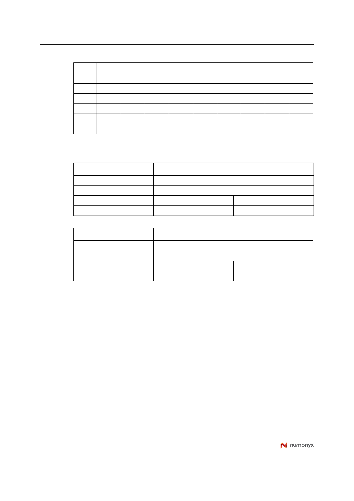
Table 1. Device summary
NAND01G-B2B
NAND02G-B2C
1-Gbit, 2-Gbit,
TSOP48 12 x 20 mm
FBGA
VFBGA63 9.5 x 12 x 1 mm
VFBGA63 9 x 11 x 1 mm
■ Serial number option
■ Data protection
– Hardware block locking
– Hardware program/erase locked during
power transitions
■ Data integrity
– 100 000 program/erase cycles per block
(with ECC)
– 10 years data retentio n
■ ECOPACK
■ Development tools
– Error correction code models
– Bad blocks management and wear lev e ling
algorithms
– Hardware simulation models
®
packages
Reference Part number
NAND01G-B2B
NAND02G-B2C
1. x16 organization only available for MCP products.
April 2008 Rev 5 1/60
NAND01GR3B2B, NAND01GW3B2B
NAND01GR4B2B, NAND01GW4B2B
NAND02GR3B2C, NAND02GW3B2C
NAND02GR4B2C, NAND02GW4B2C
www.numonyx.com
(1)
(1)
1
Page 2

Contents NAND01G-B2B, NAND02G-B2C
Contents
1 Description . . . . . . . . . . . . . . . . . . . . . . . . . . . . . . . . . . . . . . . . . . . . . . . . . 7
2 Memory array organization . . . . . . . . . . . . . . . . . . . . . . . . . . . . . . . . . . 12
2.1 Bad blocks . . . . . . . . . . . . . . . . . . . . . . . . . . . . . . . . . . . . . . . . . . . . . . . . 12
3 Signals description . . . . . . . . . . . . . . . . . . . . . . . . . . . . . . . . . . . . . . . . . 14
3.1 Inputs/outputs (I/O0-I/O7) . . . . . . . . . . . . . . . . . . . . . . . . . . . . . . . . . . . . . 14
3.2 Inputs/outputs (I/O8-I/O15) . . . . . . . . . . . . . . . . . . . . . . . . . . . . . . . . . . . . 14
3.3 Address Latch Enable (AL) . . . . . . . . . . . . . . . . . . . . . . . . . . . . . . . . . . . 14
3.4 Command Latch Enable (CL) . . . . . . . . . . . . . . . . . . . . . . . . . . . . . . . . . . 14
3.5 Chip Enable (E
3.6 Read Enable (R
3.7 Write Enable (W
3.8 Write Protect (WP
3.9 Ready/Busy (RB
3.10 V
3.11 V
supply voltage . . . . . . . . . . . . . . . . . . . . . . . . . . . . . . . . . . . . . . . . . . 15
DD
ground . . . . . . . . . . . . . . . . . . . . . . . . . . . . . . . . . . . . . . . . . . . . . . . . 15
SS
) . . . . . . . . . . . . . . . . . . . . . . . . . . . . . . . . . . . . . . . . . . . . 14
) . . . . . . . . . . . . . . . . . . . . . . . . . . . . . . . . . . . . . . . . . . . . 14
) . . . . . . . . . . . . . . . . . . . . . . . . . . . . . . . . . . . . . . . . . . . 15
) . . . . . . . . . . . . . . . . . . . . . . . . . . . . . . . . . . . . . . . . . . 15
) . . . . . . . . . . . . . . . . . . . . . . . . . . . . . . . . . . . . . . . . . . . 15
4 Bus operations . . . . . . . . . . . . . . . . . . . . . . . . . . . . . . . . . . . . . . . . . . . . 16
4.1 Command input . . . . . . . . . . . . . . . . . . . . . . . . . . . . . . . . . . . . . . . . . . . . 16
4.2 Address input . . . . . . . . . . . . . . . . . . . . . . . . . . . . . . . . . . . . . . . . . . . . . . 16
4.3 Data input . . . . . . . . . . . . . . . . . . . . . . . . . . . . . . . . . . . . . . . . . . . . . . . . . 16
4.4 Data output . . . . . . . . . . . . . . . . . . . . . . . . . . . . . . . . . . . . . . . . . . . . . . . . 16
4.5 Write Protect . . . . . . . . . . . . . . . . . . . . . . . . . . . . . . . . . . . . . . . . . . . . . . 17
4.6 Standby . . . . . . . . . . . . . . . . . . . . . . . . . . . . . . . . . . . . . . . . . . . . . . . . . . 17
5 Command set . . . . . . . . . . . . . . . . . . . . . . . . . . . . . . . . . . . . . . . . . . . . . . 19
6 Device operations . . . . . . . . . . . . . . . . . . . . . . . . . . . . . . . . . . . . . . . . . . 20
6.1 Read memory array . . . . . . . . . . . . . . . . . . . . . . . . . . . . . . . . . . . . . . . . . 20
6.1.1 Random read . . . . . . . . . . . . . . . . . . . . . . . . . . . . . . . . . . . . . . . . . . . . . 20
6.1.2 Page read . . . . . . . . . . . . . . . . . . . . . . . . . . . . . . . . . . . . . . . . . . . . . . . 20
2/60
Page 3

NAND01G-B2B, NAND02G-B2C Contents
6.2 Cache read . . . . . . . . . . . . . . . . . . . . . . . . . . . . . . . . . . . . . . . . . . . . . . . . 23
6.3 Page program . . . . . . . . . . . . . . . . . . . . . . . . . . . . . . . . . . . . . . . . . . . . . . 24
6.3.1 Sequential input . . . . . . . . . . . . . . . . . . . . . . . . . . . . . . . . . . . . . . . . . . . 24
6.3.2 Random data input in a page . . . . . . . . . . . . . . . . . . . . . . . . . . . . . . . . . 24
6.4 Copy back program . . . . . . . . . . . . . . . . . . . . . . . . . . . . . . . . . . . . . . . . . 26
6.5 Cache program . . . . . . . . . . . . . . . . . . . . . . . . . . . . . . . . . . . . . . . . . . . . . 28
6.6 Block erase . . . . . . . . . . . . . . . . . . . . . . . . . . . . . . . . . . . . . . . . . . . . . . . . 29
6.7 Reset . . . . . . . . . . . . . . . . . . . . . . . . . . . . . . . . . . . . . . . . . . . . . . . . . . . . 29
6.8 Read status register . . . . . . . . . . . . . . . . . . . . . . . . . . . . . . . . . . . . . . . . . 30
6.8.1 Write protection bit (SR7) . . . . . . . . . . . . . . . . . . . . . . . . . . . . . . . . . . . 30
6.8.2 P/E/R controller and cache ready/busy bit (SR6) . . . . . . . . . . . . . . . . . 30
6.8.3 P/E/R controller bit (SR5) . . . . . . . . . . . . . . . . . . . . . . . . . . . . . . . . . . . 30
6.8.4 Cache program error bit (SR1) . . . . . . . . . . . . . . . . . . . . . . . . . . . . . . . 31
6.8.5 Error bit (SR0) . . . . . . . . . . . . . . . . . . . . . . . . . . . . . . . . . . . . . . . . . . . . 31
6.8.6 SR4, SR3 and SR2 are reserved . . . . . . . . . . . . . . . . . . . . . . . . . . . . . . 31
6.9 Read electronic signature . . . . . . . . . . . . . . . . . . . . . . . . . . . . . . . . . . . . . 32
7 Data protection . . . . . . . . . . . . . . . . . . . . . . . . . . . . . . . . . . . . . . . . . . . . 34
8 Software algorithms . . . . . . . . . . . . . . . . . . . . . . . . . . . . . . . . . . . . . . . . 35
8.1 Bad block management . . . . . . . . . . . . . . . . . . . . . . . . . . . . . . . . . . . . . . 35
8.2 NAND flash memory failure modes . . . . . . . . . . . . . . . . . . . . . . . . . . . . . 35
8.3 Garbage collection . . . . . . . . . . . . . . . . . . . . . . . . . . . . . . . . . . . . . . . . . . 37
8.4 Wear-leveling algorithm . . . . . . . . . . . . . . . . . . . . . . . . . . . . . . . . . . . . . . 37
8.5 Error correction code . . . . . . . . . . . . . . . . . . . . . . . . . . . . . . . . . . . . . . . . 37
8.6 Hardware simulation models . . . . . . . . . . . . . . . . . . . . . . . . . . . . . . . . . . 38
8.6.1 Behavioral simulation models . . . . . . . . . . . . . . . . . . . . . . . . . . . . . . . . 38
8.6.2 IBIS simulations models . . . . . . . . . . . . . . . . . . . . . . . . . . . . . . . . . . . . 38
9 Program and erase times and endurance cycles . . . . . . . . . . . . . . . . . 39
10 Maximum ratings . . . . . . . . . . . . . . . . . . . . . . . . . . . . . . . . . . . . . . . . . . . 40
11 DC and AC parameters . . . . . . . . . . . . . . . . . . . . . . . . . . . . . . . . . . . . . . 41
11.1 Ready/Busy signal electrical characteristics . . . . . . . . . . . . . . . . . . . . . . 52
11.2 Data protection . . . . . . . . . . . . . . . . . . . . . . . . . . . . . . . . . . . . . . . . . . . . . 54
3/60
Page 4

Contents NAND01G-B2B, NAND02G-B2C
12 Package mechanical . . . . . . . . . . . . . . . . . . . . . . . . . . . . . . . . . . . . . . . . 55
13 Ordering information . . . . . . . . . . . . . . . . . . . . . . . . . . . . . . . . . . . . . . . 58
14 Revision history . . . . . . . . . . . . . . . . . . . . . . . . . . . . . . . . . . . . . . . . . . . 59
4/60
Page 5

NAND01G-B2B, NAND02G-B2C List of tables
List of tables
Table 1. Device summary. . . . . . . . . . . . . . . . . . . . . . . . . . . . . . . . . . . . . . . . . . . . . . . . . . . . . . . . . . 1
Table 2. Product description. . . . . . . . . . . . . . . . . . . . . . . . . . . . . . . . . . . . . . . . . . . . . . . . . . . . . . . . 8
Table 3. Signal names . . . . . . . . . . . . . . . . . . . . . . . . . . . . . . . . . . . . . . . . . . . . . . . . . . . . . . . . . . . . 9
Table 4. Valid blocks. . . . . . . . . . . . . . . . . . . . . . . . . . . . . . . . . . . . . . . . . . . . . . . . . . . . . . . . . . . . . 12
Table 5. Bus operations . . . . . . . . . . . . . . . . . . . . . . . . . . . . . . . . . . . . . . . . . . . . . . . . . . . . . . . . . . 17
Table 6. Address insertion, x8 devices . . . . . . . . . . . . . . . . . . . . . . . . . . . . . . . . . . . . . . . . . . . . . . . 17
Table 7. Address insertion, x16 devices . . . . . . . . . . . . . . . . . . . . . . . . . . . . . . . . . . . . . . . . . . . . . . 18
Table 8. Address definitions, x8 . . . . . . . . . . . . . . . . . . . . . . . . . . . . . . . . . . . . . . . . . . . . . . . . . . . . 18
Table 9. Address definitions, x16 . . . . . . . . . . . . . . . . . . . . . . . . . . . . . . . . . . . . . . . . . . . . . . . . . . . 18
Table 10. Commands . . . . . . . . . . . . . . . . . . . . . . . . . . . . . . . . . . . . . . . . . . . . . . . . . . . . . . . . . . . . . 19
Table 11. Copy back program x8 addresses . . . . . . . . . . . . . . . . . . . . . . . . . . . . . . . . . . . . . . . . . . . 26
Table 12. Copy back program x16 addresses . . . . . . . . . . . . . . . . . . . . . . . . . . . . . . . . . . . . . . . . . . 26
Table 13. Status register bits . . . . . . . . . . . . . . . . . . . . . . . . . . . . . . . . . . . . . . . . . . . . . . . . . . . . . . . 31
Table 14. Electronic signature . . . . . . . . . . . . . . . . . . . . . . . . . . . . . . . . . . . . . . . . . . . . . . . . . . . . . . 32
Table 15. Electronic signature byte 3 . . . . . . . . . . . . . . . . . . . . . . . . . . . . . . . . . . . . . . . . . . . . . . . . . 32
Table 16. Electronic signature byte/word 4. . . . . . . . . . . . . . . . . . . . . . . . . . . . . . . . . . . . . . . . . . . . . 33
Table 17. NAND flash failure modes . . . . . . . . . . . . . . . . . . . . . . . . . . . . . . . . . . . . . . . . . . . . . . . . . 36
Table 18. Program, erase times and program erase endurance cycles. . . . . . . . . . . . . . . . . . . . . . . 39
Table 19. Absolute maximum ratings . . . . . . . . . . . . . . . . . . . . . . . . . . . . . . . . . . . . . . . . . . . . . . . . . 40
Table 20. Operating and AC measurement conditions. . . . . . . . . . . . . . . . . . . . . . . . . . . . . . . . . . . . 41
Table 21. Capacitance . . . . . . . . . . . . . . . . . . . . . . . . . . . . . . . . . . . . . . . . . . . . . . . . . . . . . . . . . . . . 41
Table 22. DC characteristics, 1.8 V devices. . . . . . . . . . . . . . . . . . . . . . . . . . . . . . . . . . . . . . . . . . . . 43
Table 23. DC characteristics, 3 V devices . . . . . . . . . . . . . . . . . . . . . . . . . . . . . . . . . . . . . . . . . . . . . 43
Table 24. AC characteristics for command, address, data input . . . . . . . . . . . . . . . . . . . . . . . . . . . . 44
Table 25. AC characteristics for operations . . . . . . . . . . . . . . . . . . . . . . . . . . . . . . . . . . . . . . . . . . . . 45
Table 26. TSOP48 - 48 lead plastic thin small outline, 12 x 20 mm, package mechanic al data . . . . . 55
Table 27. VFBGA63 9.5 x 12 mm - 6 x 8 ball array, 0.80 mm pitch, package mechanical data. . . . . 56
Table 28. VFBGA63 9 x 11 mm - 6 x 8 active ball array, 0.80 mm pitch, package mechanical data. 57
Table 29. Ordering information scheme . . . . . . . . . . . . . . . . . . . . . . . . . . . . . . . . . . . . . . . . . . . . . . . 58
Table 30. Document revision history . . . . . . . . . . . . . . . . . . . . . . . . . . . . . . . . . . . . . . . . . . . . . . . . . 59
5/60
Page 6

List of figures NAND01G-B2B, NAND02G-B2C
List of figures
Figure 1. Logic block diagram . . . . . . . . . . . . . . . . . . . . . . . . . . . . . . . . . . . . . . . . . . . . . . . . . . . . . . . 8
Figure 2. Logic diagram . . . . . . . . . . . . . . . . . . . . . . . . . . . . . . . . . . . . . . . . . . . . . . . . . . . . . . . . . . . . 9
Figure 3. TSOP48 connections . . . . . . . . . . . . . . . . . . . . . . . . . . . . . . . . . . . . . . . . . . . . . . . . . . . . . 10
Figure 4. VFBGA63 connections (top view through package). . . . . . . . . . . . . . . . . . . . . . . . . . . . . . 11
Figure 5. Memory array organization . . . . . . . . . . . . . . . . . . . . . . . . . . . . . . . . . . . . . . . . . . . . . . . . . 13
Figure 6. Read operations . . . . . . . . . . . . . . . . . . . . . . . . . . . . . . . . . . . . . . . . . . . . . . . . . . . . . . . . . 21
Figure 7. Random data output during sequential data output . . . . . . . . . . . . . . . . . . . . . . . . . . . . . . 22
Figure 8. Cache read operation . . . . . . . . . . . . . . . . . . . . . . . . . . . . . . . . . . . . . . . . . . . . . . . . . . . . . 23
Figure 9. Page program operation . . . . . . . . . . . . . . . . . . . . . . . . . . . . . . . . . . . . . . . . . . . . . . . . . . . 25
Figure 10. Random data input during sequential data input . . . . . . . . . . . . . . . . . . . . . . . . . . . . . . . . 25
Figure 11. Copy back program . . . . . . . . . . . . . . . . . . . . . . . . . . . . . . . . . . . . . . . . . . . . . . . . . . . . . . 27
Figure 12. Page copy back program with random data input . . . . . . . . . . . . . . . . . . . . . . . . . . . . . . . 27
Figure 13. Cache program operation . . . . . . . . . . . . . . . . . . . . . . . . . . . . . . . . . . . . . . . . . . . . . . . . . . 28
Figure 14. Block erase operation. . . . . . . . . . . . . . . . . . . . . . . . . . . . . . . . . . . . . . . . . . . . . . . . . . . . . 29
Figure 15. Bad block management flowchart. . . . . . . . . . . . . . . . . . . . . . . . . . . . . . . . . . . . . . . . . . . . 36
Figure 16. Garbage collection . . . . . . . . . . . . . . . . . . . . . . . . . . . . . . . . . . . . . . . . . . . . . . . . . . . . . . . 36
Figure 17. Error detection . . . . . . . . . . . . . . . . . . . . . . . . . . . . . . . . . . . . . . . . . . . . . . . . . . . . . . . . . . 38
Figure 18. Equivalent testing circuit for AC characteristics measurement. . . . . . . . . . . . . . . . . . . . . . 42
Figure 19. Command latch AC waveforms . . . . . . . . . . . . . . . . . . . . . . . . . . . . . . . . . . . . . . . . . . . . . 46
Figure 20. Address latch AC waveforms . . . . . . . . . . . . . . . . . . . . . . . . . . . . . . . . . . . . . . . . . . . . . . . 46
Figure 21. Data Input Latch AC waveforms. . . . . . . . . . . . . . . . . . . . . . . . . . . . . . . . . . . . . . . . . . . . . 47
Figure 22. Sequential data output after read AC waveforms. . . . . . . . . . . . . . . . . . . . . . . . . . . . . . . . 47
Figure 23. Read status register AC waveforms. . . . . . . . . . . . . . . . . . . . . . . . . . . . . . . . . . . . . . . . . . 48
Figure 24. Read electronic signature AC waveforms. . . . . . . . . . . . . . . . . . . . . . . . . . . . . . . . . . . . . . 48
Figure 25. Page read operation AC waveforms. . . . . . . . . . . . . . . . . . . . . . . . . . . . . . . . . . . . . . . . . . 49
Figure 26. Page program AC waveforms. . . . . . . . . . . . . . . . . . . . . . . . . . . . . . . . . . . . . . . . . . . . . . . 50
Figure 27. Block erase AC waveforms. . . . . . . . . . . . . . . . . . . . . . . . . . . . . . . . . . . . . . . . . . . . . . . . . 51
Figure 28. Reset AC waveforms . . . . . . . . . . . . . . . . . . . . . . . . . . . . . . . . . . . . . . . . . . . . . . . . . . . . . 51
Figure 29. Program/erase enable waveforms . . . . . . . . . . . . . . . . . . . . . . . . . . . . . . . . . . . . . . . . . . . 52
Figure 30. Program/erase disable waveforms. . . . . . . . . . . . . . . . . . . . . . . . . . . . . . . . . . . . . . . . . . . 52
Figure 31. Ready/Busy AC waveform . . . . . . . . . . . . . . . . . . . . . . . . . . . . . . . . . . . . . . . . . . . . . . . . . 53
Figure 32. Ready/Busy load circuit . . . . . . . . . . . . . . . . . . . . . . . . . . . . . . . . . . . . . . . . . . . . . . . . . . . 53
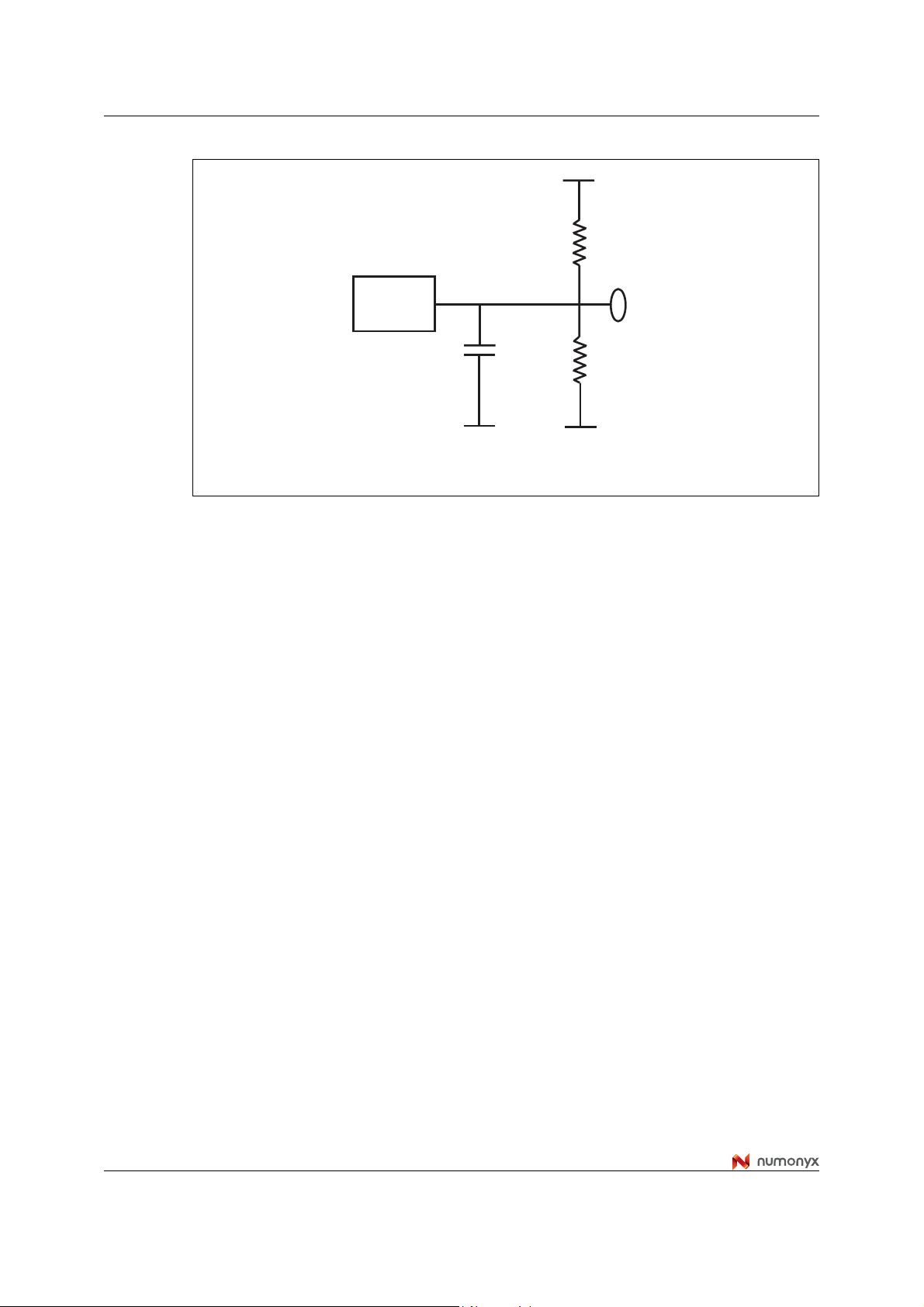
Figure 33. Resistor value versus waveform timings for Ready/Busy signal. . . . . . . . . . . . . . . . . . . . . 54
Figure 34. Data protection . . . . . . . . . . . . . . . . . . . . . . . . . . . . . . . . . . . . . . . . . . . . . . . . . . . . . . . . . 54
Figure 35. TSOP48 - 48 lead plastic thin small outline, 12 x 20 mm, package outline . . . . . . . . . . . . 55
Figure 36. VFBGA63 9.5 x 12 mm - 6 x 8 active ball array, 0.80 mm pitch, package outline . . . . . . . 56
Figure 37. VFBGA63 9 x 11 mm - 6 x 8 active ball array, 0.80 mm pitch, package outline. . . . . . . . . 57
6/60
Page 7

NAND01G-B2B, NAND02G-B2C Description
1 Description
NAND01G-B2B and NAND02G-B2C flash 2112-byte/1056-word page is a family of nonvolatile flash memories that uses NAND cell technology. The devices range from 1 Gbit to 2
Gbits and operate with either a 1.8 V or 3 V vo ltage supply. The size of a page is either 2112
bytes (2048 + 64 spare) or 1056 w ords (1 024 + 32 spar e) dep ending on whet her the device
has a x8 or x16 bus width.
The address lines are multiplexed with the Data Input/Output signals on a multiplexed x8 or
x16 input/output bus. This interface reduces the pin count and makes it possible to migrate
to other densities without changing the footprint.
Each block can be programmed and erased over 100 000 cycles (with ECC on). To extend
the lifetime of NAND flash devices it is strongly recommended to implement an error
correction code (ECC).
The devices feature a write protect pin that allows performing hardware protection against
program and erase operations.
The devices feature an open-drain ready/busy output that can be used to identify if the
program/erase/read (P/E/R) controller is currently active. The use of an open-drain output
allows the ready/busy pins from several memories to be connected to a single pull-up
resistor.
A Copy Back Program command is av ailable to optimize the management of defective
blocks. When a page prog r am oper ation fails, the data can be pr ogr a mmed in ano ther pag e
without having to resend the data to be programmed.
Each device has cache program and cache read features which improve t he program and
read throughputs for lar ge files. During cache programming, the device loads the data in a
cache register while the pre vious data is tr ansf erred to the page b uff er and progr ammed into
the memory array. During cache reading, the de vice loads the data in a cache register while
the previous data is transferred to the I/O buffers to be read.
All devices have the chip enable don’t care feature, which allows code to be directly
downloaded by a microcontroller, as chip enable transitions during the latency time do no t
stop the read operation.
All devices have the option of a unique identifier (serial number), which allows each device
to be uniquely identified.
The unique identifier options is subject to an NDA (non disclosure agreement) and so not
described in the datasheet. For more details of this option contact your nearest Numonyx
sales office.
The devices are available in the following packages:
● TSOP48 (12 x 20 mm)
● VFBGA63 (9.5 x 12 x 1 mm, 0.8 mm pitch) for NAND02G-B2C devices
● VFBGA63 (9 x 11 x 1 mm, 0.8 mm pitch) for NAND01G-B2B devices.
For information on how to order these options refer to Table 29: Ordering information
scheme. Devices are shipped from the factory with Block 0 always valid and the memory
content bits, in valid blocks, erased to ’1’.
See Table 2: Product description, for all the devices available in the family.
7/60
Page 8
Description NAND01G-B2B, NAND02G-B2C
Table 2. Product description
Reference Part number Den s it y
NAND01G
-B2B
NAND02G
-B2C
NAND01GR3B2B
NAND01GW3B2B
NAND01GR4B2B
NAND01GW4B2B
NAND02GR3B2C
NAND02GW3B2C
NAND02GR4B2C
NAND02GW4B2C
Bus
width
x8
1Gbit
x16
x8
2Gbits
x16
1. x16 organization only available for MCP.
Page
size
2048
+64
bytes
1024
+32
words
2048
+64
bytes
1024
+32
words
Block
size
128K
+4K
bytes
64K+
2K
words
128K
+4K
bytes
64K+
2K
words
Memory
array
64
pages x
1024
blocks
64
pages x
2048
blocks
Operating
voltage
1.7 to
1.95 V
2.7 to
3.6 V
1.7 to
1.95 V
2.7 to
3.6 V
1.7 to
1.95 V
2.7 to
3.6 V
1.7 to
1.95 V
2.7 to
3.6 V
Timings
Random
access
Sequential
time
(max)
25 µs 50 ns
25 µs 30 ns TSOP48
25 µs 50 ns
25 µs 30 ns
25 µs 50 ns
25 µs 30 ns TSOP48
25 µs 50 ns
25 µs 30 ns
access
time
(min)
Page
Progra
m time
(typ)
200 µs
Bloc
k
erase
(typ)
2ms
2ms
Package
VFBGA63
9x11mm
VFBGA63
9.5 x 12 m
(1)
(1)
m
(1)
(1)
Figure 1. Logic block diagram
Address
register/counter
AL
CL
W
E
WP
R
Command
interface
logic
Command register
P/E/R controller,
high voltage
generator
RB
NAND flash
memory array
X decoder
Page buffer
Cache register
Y decoder
I/O buffers & latches
I/O0-I/O7, x8/x16
I/O8-I/O15, x16
AI12799
8/60
Page 9
NAND01G-B2B, NAND02G-B2C Description
Figure 2. Logic diagram
V
DD
E
R
W
AL
CL
WP
1. x16 organization only available for MCP.
Table 3. Signal names
Signal Function Direction
I/O8-15 Data input/outputs for x16 devices I/O
I/O0-7
Data input/outputs, address inputs, or command inputs
for x8 and x16 devices
AL Address Latch Enable Input
NAND01G-B2B
NAND02G-B2C
V
SS
I/O8-I/O15, x16
I/O0-I/O7, x8/x16
RB
AI13101
I/O
CL Command Latch Enable Input
E
R
RB
W
WP
V
V
DD
SS
Chip Enable Input
Read Enable Input
Ready/Busy (open-drain output) Output
Write Enable Input
Write Protect Input
Supply voltage Supply
Ground Supply
NC Not connected internally –
DU Do not use –
9/60
Page 10
Description NAND01G-B2B, NAND02G-B2C
Figure 3. TSOP48 connections
V
V
WP
NC
NC
NC
NC
NC
NC
RB
NC
NC
DD
SS
NC
NC
CL
AL
NC
NC
NC
NC
NC
1
R
E
NAND01GW3B2B
12
NAND02GW3B2C
13
W
24 25
48
37
36
NC
NC
NC
NC
I/O7
I/O6
I/O5
I/O4
NC
NC
NC
V
DD
V
SS
NC
NC
NC
I/O3
I/O2
I/O1
I/O0
NC
NC
NC
NC
1. Available only for NAND01GW3B2B and NAND02GW3B2C 8-bit devices.
10/60
AI13102
Page 11
NAND01G-B2B, NAND02G-B2C Description
Figure 4. VFBGA63 connections (top vie w through package)
87654321
A
B
C
D
E
F
G
DU DU
DU
WP
NC
NC NC
AL
NCNC
NC
DU
DU
V
SS
R
CL
NC
NC
NCNC
NC
NC
E
W
NC
NC
NC
NCNC
RB
NCNC
NC
NC
NC
109
DU
DU
H
J
K
L
M
DU DU
DU
DU
NC
NC
V
SS
I/O0
I/O1
I/O2
NC
NC
DD
I/O4I/O3
1. Available only for NAND01GR3B2B and NAND02GR3B2C 8-bit devices.
NCNC
I/O5V
I/O6
V
DD
I/O7
V
SS
DU DU
DU
DU
AI13103
11/60
Page 12
Memory array organization NAND01G-B2B, NAND02G-B2C
2 Memory array organization
The memory array is made up of NAND structures wh er e 32 cells are co nn ected in series.
The memory array is organized in blocks where each block contains 64 pages. The array is
split into two areas, the main ar ea and t he spa re area . The main are a of th e array is used to
store data whereas the spare area is typically used to store e rror correction cod es, softw are
flags or bad block identification.
In x8 devices the pages are split in to a 2048-b yte main are a and a spare area of 64 b ytes. In
the x16 devices the pages are split into a 1,024-word main area and a 32-word spare area.
Refer to Figure 5: Memory array organization.
2.1 Bad blocks
The NAND flash 2112-byte/1056-word page devices may contain bad blocks, that is blocks
that contain one or more invalid bits whose reliability is not guaranteed. Additional bad
blocks may develop during the lifetime of the device.
The bad block Information is written prior to shipping (refer to Section 8.1: Bad block
management for more details).
Table 4: Valid blocks shows the minimum number of valid blocks in each device. The values
shown include both the bad blocks that are present when the de vice is shipped and t he bad
blocks that could develop later on.
These blocks need to be managed using bad blocks management, block replacement or
error correction codes (refer to Section 8: Software algorithms).
Table 4. Valid blocks
Density of device Min Max
2 Gbits 2008 2048
1 Gbit 1004 1024
12/60
Page 13
NAND01G-B2B, NAND02G-B2C Memory array organization
Figure 5. Memory array organization
x8 DEVICES x16 DEVICES
Block = 64 pages
Page = 2112 bytes (2,048 + 64)
Block = 64 pages
Page = 1056 words (1024 + 32)
Block
Page
Main area
2048 bytes
bytes
Page buffer, 2112 bytes
2,048 bytes
64
64
bytes
Spare area
8 bits
8 bits
Block
Page
Main area
1024 words
Page buffer, 1056 words
1,024 words
32
words
32
words
Spare area
16 bits
16 bits
AI09854
13/60
Page 14

Signals description NAND01G-B2B, NAND02G-B2C
3 Signals description
See Figure 2: Logic diagram, and Table 3: Signal names, for a brief overview of the signals
connected to this device.
3.1 Inputs/outputs (I/O0-I/O7)
Input/outputs 0 to 7 are used to input the selected address, output the data during a read
operation or input a command or data during a write operation. The inputs are latched on
the rising edge of Write Enable. I/O0-I/O7 are left floating when the device is deselected or
the outputs are disabled.
3.2 Inputs/outputs (I/O8-I/O15)
Input/outputs 8 to 15 are only available in x16 devices. They are used to output the data
during a read operation or input data during a write operation. Comma nd and address
Inputs only require I/O0 to I/O7.
The inputs are latched on the rising edge of Write Enable. I/O8-I/O15 are left floating when
the device is deselected or the outputs are disabled.
3.3 Address Latch Enable (AL)
The Address Latch Enable activates the latching of the address inputs in the command
interface. When AL is High, the inputs are latched on the rising edge of Write Enable.
3.4 Command Latch Enable (CL)
The Command Latch Enable activates the latching of the command inputs in the command
interface. When CL is High, the inputs are latched on the rising edge of Write Enable .
3.5 Chip Enable (E)
The Chip Enable input activates the memory control logic, input buffers, decoders and
sense amplifiers. When Chip Enable is Low, V
High, v
mode.
, while the device is busy, the device remains selected and does not go into standb y
IH
3.6 Read Enable (R)
The Read Enable pin, R, controls the sequential data output during read oper atio ns. Data is
valid t
column address counter by one.
after the falling edge of R. The falling edge of R also increments the internal
RLQV
, the device is selected. If Chip Enable goes
IL
14/60
Page 15

NAND01G-B2B, NAND02G-B2C Signals description
3.7 Write Enable (W)
The Write Enable input, W, controls writing to the command interface, input address and
data latches. Both addresses a nd data are latched on the rising edge of Write Enable.
During power-up and power-down a recovery time of 10 µs (min) is required before the
command interface is ready t o accept a co mmand. It is r ecommended t o k eep Write Enab le
High during the recovery time.
3.8 Write Protect (WP)
The Write Protect pin is an input that giv es a hardware protect ion against unwanted program
or erase operations. When Write Protect is Low , V
program or erase operations.
, the device does not accept any
IL
It is recommended to keep the Write Protect pin Lo w, V
3.9 Ready/Busy (RB)
The Ready/Busy output, RB, is an open- drain outp ut that can be u sed to identif y if the P/E/R
controller is currently active. When Ready/Busy is Low, V
operation is in progress. When the operation completes Ready/Busy goes High, V
The use of an open-drain output allows the Ready/Busy pins from several memories to be
connected to a single pull-up resistor. A Low will then indicate that one, or more, of the
memories is busy.
Refer to the Section 11.1: Ready/Busy signal electrical characteristics for details on how to
calculate the value of the pull-up resistor.
During power-up and power-down a minimum recovery time of 10 µs is required before the
command interface is ready to accept a command. During this period the RB
V
.
OL
3.10 V
supply voltage
DD
VDD provides the power supply to the internal core of the memory device. It is the main
power supply for all operations (read, program and erase).
An internal voltage detector disables all functions whenever V
Table 22 and Table 23) to protect the device from any involuntary program/erase during
power-transitions.
, during power-up and po w er-do wn.
IL
, a read, program or erase
OL
is below V
DD
signal is Low,
LKO
OH
(see
.
Each device in a system should have V
widths should be sufficient to carry the required program and erase currents.
3.11 VSS ground
Ground, V
ground.
is the reference for the power supply. It must be connected to the system
SS,
decoupled with a 0.1 µF capacitor. The PCB track
DD
15/60
Page 16

Bus operations NAND01G-B2B, NAND02G-B2C
4 Bus operations
There are six standard bus operations that control the memory. Each of these is described
in this section, see Table 5: Bus operations, for a summary.
Typically, glitches of less than 5 ns on Chip Enable, Write Enable and Read Enable are
ignored by the memory and do not affect bus operations.
4.1 Command input
Command input bus operations are used to giv e comm ands to the me mory. Commands are
accepted when Chip Enable is Low, Command Latch Enable is High, Address Latch Enable
is Low and Read Enable is High. They are latched on the rising edge of the Write Enable
signal.
Only I/O0 to I/O7 are used to input commands.
See Figure 19 and Table 24 for details of the timings requirements.
4.2 Address input
Address input bus operati ons are used to inpu t the me mory addresses. Four bus cycles are
required to input the addresses for 1-Gbit devices whereas five bus cycles are required for
the 2-Gbit device (refer to Table 6 and Table 7, Address insertion).
The addresses are accepted when Chip Enable is Low , Address Latch Enable is High,
Command Latch Enable is Low and Read Enable is High. They are latched on the rising
edge of the Write Enable signal. Only I/O0 to I/O7 are used to input add resse s.
See Figure 20 and Table 24 for details of the timings requirements.
4.3 Data input
Data input bus operations are used to input the data to be programmed.
Data is accepted only when Chip Enable is Low, Address Latch Enable is Low, Command
Latch Enable is Low and Read Enable is High. The data is latched on the rising edge of the
Write Enable signal. The data is input sequentially using the Write Enab le signal.
See Figure 21 and Table 24 and Table 25 for details of the timings requirements.
4.4 Data output
Data output bus operations are used to read: the data in the memory array, the status
register, the lock status, the electronic signature and the unique identifier.
Data is output when Chip Enable is Low , Write Enable is High, Address Latch Enable is Low,
and Command Latch Enable is Low. The data is output sequentially using the Read Enable
signal.
See Figure 22 and Table 25 for details of the timings requirements.
16/60
Page 17
NAND01G-B2B, NAND02G-B2C Bus operations
4.5 Write Protect
Write Protect bus operations are used to protect the memory against program or erase
operations. When the Write Protect signal is Low the device will not accept progr am or erase
operations and so the contents of the memory array cannot be altered. The Write Protect
signal is not latched by Write Enable to ensure protection even during power-up.
4.6 Standby
When Chip Enable is High the memory enters standby mode, the device is deselected,
outputs are disabled and po wer consumption is reduced.
Table 5. Bus operations
Bus operation E AL CL R W WP I/O0 - I/O7 I/O8 - I/O15
Command input V
Address input V
Data input V
Data output V
V
IL
V
IL
V
IL
V
IL
V
IL
V
IH
V
IL
V
IL
IH
IL
IL
IL
V
Rising X
IH
V
Rising X Address X
IH
V
Rising V
IH
Falling V
IH
Write Protect X X X X X V
Standby V
XXX X
IH
(2)
Command X
Data input Data input
IH
X Data output Data output
XX
XX
V
IL/VD
IL
D
1. Only for x16 devices.
2. WP must be VIH when issuing a program or erase command.
Table 6. Address insertion, x8 devices
5
1
nd
2
3
4
th(2)
(1)
I/O7 I/O6 I/O5 I/O4 I/O3 I/O2 I/O1 I/O0
st
rd
th
A7 A6 A5 A4 A3 A2 A1 A0
V
IL
V
IL
V
IL
V
IL
A11 A10 A9 A8
A19 A18 A17 A16 A15 A14 A13 A12
A27 A26 A25 A24 A23 A22 A21 A20
V
IL
V
IL
V
IL
V
IL
V
IL
V
IL
V
IL
Bus cycle
1. Any additional address input cycles will be ignored.
2. The fifth cycle is valid for 2-Gbit devices. A28 is for 2-Gbit devices only.
(1)
A28
17/60
Page 18
Bus operations NAND01G-B2B, NAND02G-B2C
Table 7. Address insertion, x16 devices
Bus
cycle
1
nd
2
rd
3
4
th(2)
5
1. Any additional address input cycles will be ignored.
2. The fifth cycle is valid for 2-Gbit devices. A27 is for 2-Gbit devices only.
Table 8. Address definitions, x8
I/O8-
(1)
I/O15
st
X A7A6A5A4A3A2A1A0
X V
I/O7 I/O6 I/O5 I/O4 I/O3 I/O2 I/O1 I/O0
IL
V
IL
V
IL
V
IL
V
X A18 A17 A16 A15 A14 A13 A12 A11
th
X A26 A25 A24 A23 A22 A21 A20 A19
X V
IL
V
IL
V
IL
V
IL
V
Address Definition
A0 - A11 Column address
A12 - A17 Page address
A18 - A27 Block address 1-Gbit device
A18 - A28 Block address 2-Gbit device
Table 9. Address definitions, x16
Address Definition
IL
IL
A10 A9 A8
V
IL
V
IL
A27
A0 - A10 Column address
A11 - A16 Page address
A17 - A26 Block address 1-Gbit device
A17 - A27 Block address 2-Gbit device
18/60
Page 19

NAND01G-B2B, NAND02G-B2C Command set
5 Command set
All bus write operations to the device are interpreted by the command interface. The
commands are input on I/O0-I/O7 and are latched on the rising edge of Write Enable when
the Command Latch Enable signal is High. Device operations are selected by writing
specific commands to the command register. The two-step command sequences for
program and erase ope rations are imposed to maximize data security.
The commands are summarized in Table 10: Commands.
Table 10. Commands
Bus write operations
Command
1st cycle 2nd cycle 3rd cycle 4th cycle
Read 00h 30h – –
Random Data Output 05h E0h – –
Cache Read 00h 31h – –
Exit Cache Read 34h – – – Yes
(1)
Commands
accepted
during
busy
(2)
Page Program
(Sequential Input default)
Random Data Input 85h – – –
Copy Back Program 00h 35h 85h 10h
Cache Program 80h 15h – –
Block Erase 60h D0h – –
Reset FFh – – – Ye s
Read Electronic Signature 90h – – –
Read Status Register 70h – – – Yes
1. The bus cycles are only shown for issuing the codes. The cycles required to input the
addresses or input/output data are not shown.
2. Only during Cache Read busy.
80h 10h – –
19/60
Page 20

Device operations NAND01G-B2B, NAND02G-B2C
6 Device operations
The following section gives the details of the device operations.
6.1 Read memory array
At power-up the device defaults to read mode. To enter read mode from another mode the
Read command must be issued, see Table 10: Commands.
Once a Read command is issued two types of operations are available: random read and
page read.
6.1.1 Random read
Each time the Read command is issued the first read is random read.
6.1.2 Page read
After the first random read access, the page data (2112 bytes or 1056 words) is transferred
to the page buffer in a time of t
complete the Ready/Busy signal goes High. The data can then be read out sequentially
(from selected column address to last column address) by pulsing the Read Enable signal.
(refer to Table 25 for value). Once the transfer is
WHBH
The device can output rando m data in a page, instead of the co nsecutive sequent ial data, by
issuing a Random Data Output command.
The Random Data Output command can be used to skip some data during a sequential
data output.
The sequential operation can be resum ed by changing the column address of th e next data
to be output, to the address which follows the Random Data Output command.
The Random Data Output command can be issued as man y times as required within a
page.
The Random Data Output command is not accepted during cach e read operations.
20/60
Page 21

NAND01G-B2B, NAND02G-B2C Device operations
Figure 6. Read operations
CL
E
W
AL
R
tBLBH1
RB
I/O
00h
Command
code
Address input
1. Highest address depends on device density.
30h
Command
code
Data output (sequentially)
Busy
ai08657b
21/60
Page 22
Device operations NAND01G-B2B, NAND02G-B2C
Figure 7. Random data output during sequential data output
tBLBH1
RB
R
(Read Busy time)
Busy
I/O
Row Add 1,2,3
00h
Cmd
code
Address
inputs
5 Add cycles
Col Add 1,2
30h
Cmd
code
Main area
Data output
Spare
area
05h
Cmd
code
Address
inputs
2Add cycles
Col Add 1,2
E0h
Cmd
code
Main area
Data output
Spare
area
ai08658
22/60
Page 23

NAND01G-B2B, NAND02G-B2C Device operations
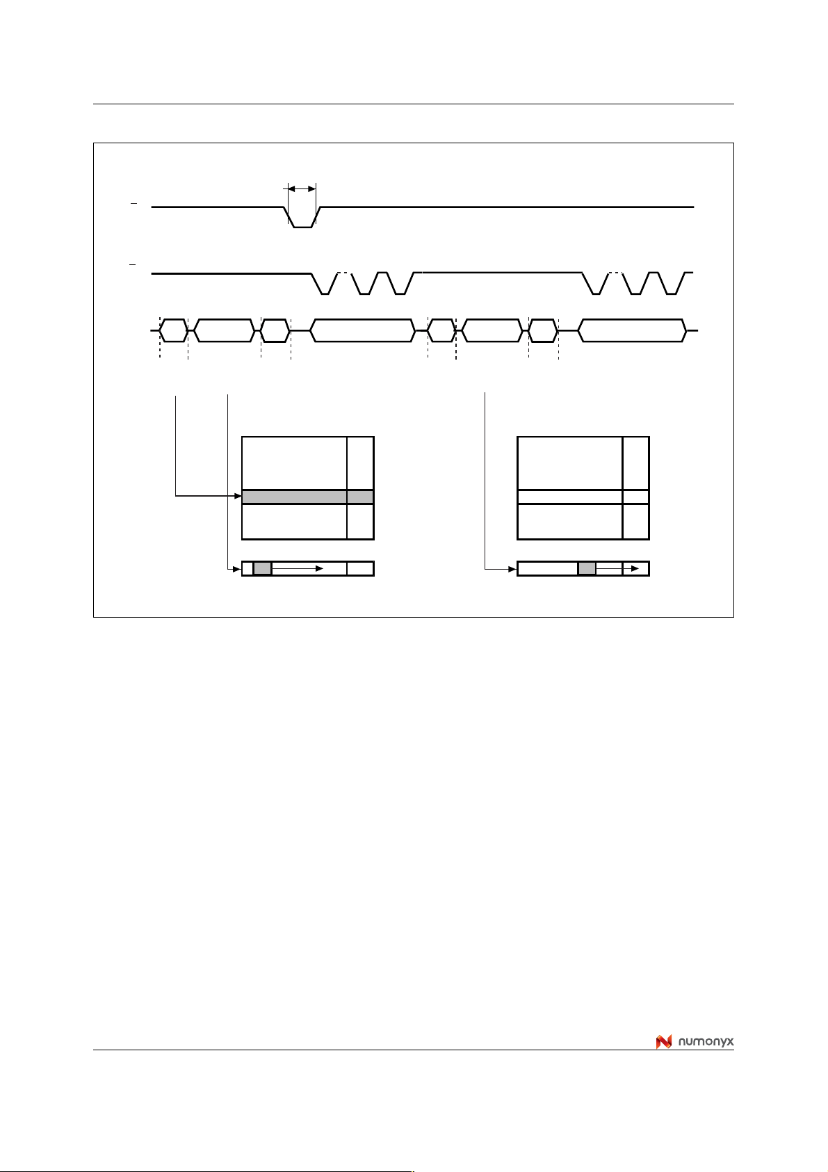
6.2 Cache read
The cache read operation is used to improve the read throughput by readin g dat a using th e
cache register. As soon as the user starts to read one page, the device automatically loads
the next page into the cache register.
A cache read operation consists of three steps (see Table 10: Commands):
1. One bus cycle is required to setup the Cache Read command (the same as the
standard Read command)
2. Four or five (refer to Table 6 and Table 7) bus cycles are then required to input the start
address
3. One bus cycle is required to issue the Cache Read Confirm command to start the
P/E/R controller.
The start address must be at the beginning of a page (column address = 00h, see Table 8
and Table 9). This allows the data to be output uninterrupted after the latency time (t
see Figure 8.
The Ready/Busy signal can be used to monitor the start of the operation. During the latency
period the Ready/Busy signal goes Low, after this the Ready/Busy signa l goes High, even if
the device is internally downloading page n+1.
Once the cache read operation has started, the status register can be read using the Read
Status Register command.
BLBH1
),
During the operation, SR5 can be read, to find out whether the internal reading is ongoing
(SR5 = ‘0’), or has completed (SR5 = ‘1’), while SR6 indicates whether the cache register is
ready to download new data.
To exit the cache read operation an Exit Cache Read command must be issued (see
Table 10).
If the Exit Cache Read command is issued while the device is internally reading page n+1,
pages n and n+1 will not be output.
Figure 8. Cache read operation
tBLBH1
(Read Busy time)
RB
R
I/O
00h
Read
Setup
code
Address
inputs
31h
Cache
Read
Confirm
code
Busy
1st page
2nd page
3rd page
Block N
Data output
last page
tBLBH4
34h
Exit
Cache
Read
code
ai13104b
23/60
Page 24

Device operations NAND01G-B2B, NAND02G-B2C
6.3 Page program
The page program oper ation is the sta ndard oper ation to prog ram data to the memory arra y.
Generally, the page is programmed sequentially, however the device does support random
input within a page. It is recommended to address pages sequentially within a given block.
The memory array is program med by page, however partial page programming is allowed
where any number of bytes (1 to 2112) or words (1 to 1056) can be programmed.
The maximum number of consecutive partial page program operations allowed in the same
page is four . After e xceeding this a Bloc k Erase command must be issued before an y further
program operations can take place in that page.
6.3.1 Sequential input
To input dat a sequentially the addresses must be sequential and remain in one block.
For sequential input each page program operation consist s of five steps (see Figure 9):
1. one bus cycle is required to setup the Page Program (sequential input) command (see
Table 10)
2. four or five bus cycles are then required to input the program address (refer to Table 6
and Table 7)
3. the data is then loaded into the data registers
4. one bus cycle is required to issue the Page Program Con firm command to start the
P/E/R controller. The P/E/R will only start if the data has been loaded in step 3
5. the P/E/R controller then programs the data into the array.
6.3.2 Random data input in a page
During a sequential input operation, the next sequential address to be programmed can be
replaced by a random addr ess, by issuing a Random Data Input command. The following
two steps are required to issue the command:
1. one bus cycle is required to setup the Random Data Input command (see Table 10)
2. two bus cycles are then required to input the new column address (refer to Table 6).
Random Data Input can be repeated as often as required in any given page.
Once the program operation has started the status register can be read using the Read
Status Register command. During program operations the status register will only flag errors
for bits set to '1' that have not been successfully programmed to '0'.
During the program operation, only th e Read Status Register and Reset commands will be
accepted, all other commands will be ignored.
Once the program operatio n has co mpleted t he P/E/R co ntroller bit SR6 is set to ‘1’ and the
Ready/Busy signal goes High.
The device remains in read status register mode until another valid command is written to
the command interface.
24/60
Page 25

NAND01G-B2B, NAND02G-B2C Device operations
Figure 9. Pa ge program operation
tBLBH2
RB
(Program Busy time)
Busy
I/O
80h
Page Program
Setup Code
Address Inputs
Data Input
Figure 10. Random data input during sequential data input
RB
I/O
80h
Cmd
Code
Address
Inputs
5 Add cycles
Col Add 1,2Row Add 1,2,3
Data Intput
Main area
Code
Spare
85h
Cmd
area
Address
Inputs
2 Add cycles
Col Add 1,2
Data Input
10h
Confirm
Code
tBLBH2
(Program Busy time)
10h
Confirm
Code
Main area
70h
Read Status Register
Busy
70h
Read Status Register
Spare
area
SR0
ai08659
SR0
ai08664
25/60
Page 26
Device operations NAND01G-B2B, NAND02G-B2C
6.4 Copy back program
The copy back program operation is used to copy the data stored in one page and
reprogram it in another page.
The copy back progr am oper ation does not req uire e xternal memory and so the operation is
faster and more efficient because the reading and loading cycles are not required. The
operation is particularly useful when a portion of a block is updated and the rest of the block
needs to be copied to the newly assigned block.
If the copy back program operation fails an error is signalled in the status register. However
as the standard external ECC cannot be used with the cop y back pr ogram oper ation bit error
due to charge loss cannot be detected. For this reason it is recommended to limit the
number of copy back program operations on the same data and or to improve the
performance of the ECC.
The copy back pr ogram operation requires four steps:
1. The first step reads the source page. The operation copies all 1056 words/ 2112 by tes
from the page into the data buffer. It requires:
– one bus write cycle to setup the command
– 4 or 5 bus write cycles to input the source page address (see Table 6 and Table 7)
– one bus write cycle to issue the confirm command code
2. When the device returns to the ready state (Ready/Busy High), the next bus write cycle
of the command is given with the 4 or 5 bus cycles to input the target page address
(see Table 6 and Table 7). Refer to Table 11 for the addresses that must be the same
for the source and target pag es
3. Then the confirm command is issued to start the P/E/R controller.
To see the data input cycle for modifying the source page and an example of the copy back
program operation refer to Figure 11.
A data input cycle to modify a portion or a multiple distant portion of the source page, is
shown in Figure 12.
Table 11. Copy back program x8 addresses
Density Same address for source and target pages
1 Gbit no constraint
2 Gbits A28
Table 12. Copy back program x16 addresses
Density Same address for source and target pages
1 Gbit no constraint
2 Gbits A27
26/60
Page 27

NAND01G-B2B, NAND02G-B2C Device operations
Figure 11. Copy back pr ogram
I/O
00h
Read
Code
Source
Add Inputs
35h
tBLBH1
(Read Busy time)
85h
Copy Back
Code
Target
Add Inputs
RB
Busy
Figure 12. Page copy back program with random data input
Target
Add Inputs
85h Data
Data
Unlimited number of repetitions
RB
I/O
00h
Read
Code
Source
Add Inputs
(Read Busy time)
35h
tBLBH1
Copy Back
Busy
85h
Code
10h 70h SR0
tBLBH2
(Program Busy time)
2 Cycle
Add Inputs
(Program Busy time)
Read Status Register
Busy
10h 70h
tBLBH2
Busy
ai09858b
SR0
ai11001
27/60
Page 28
Device operations NAND01G-B2B, NAND02G-B2C
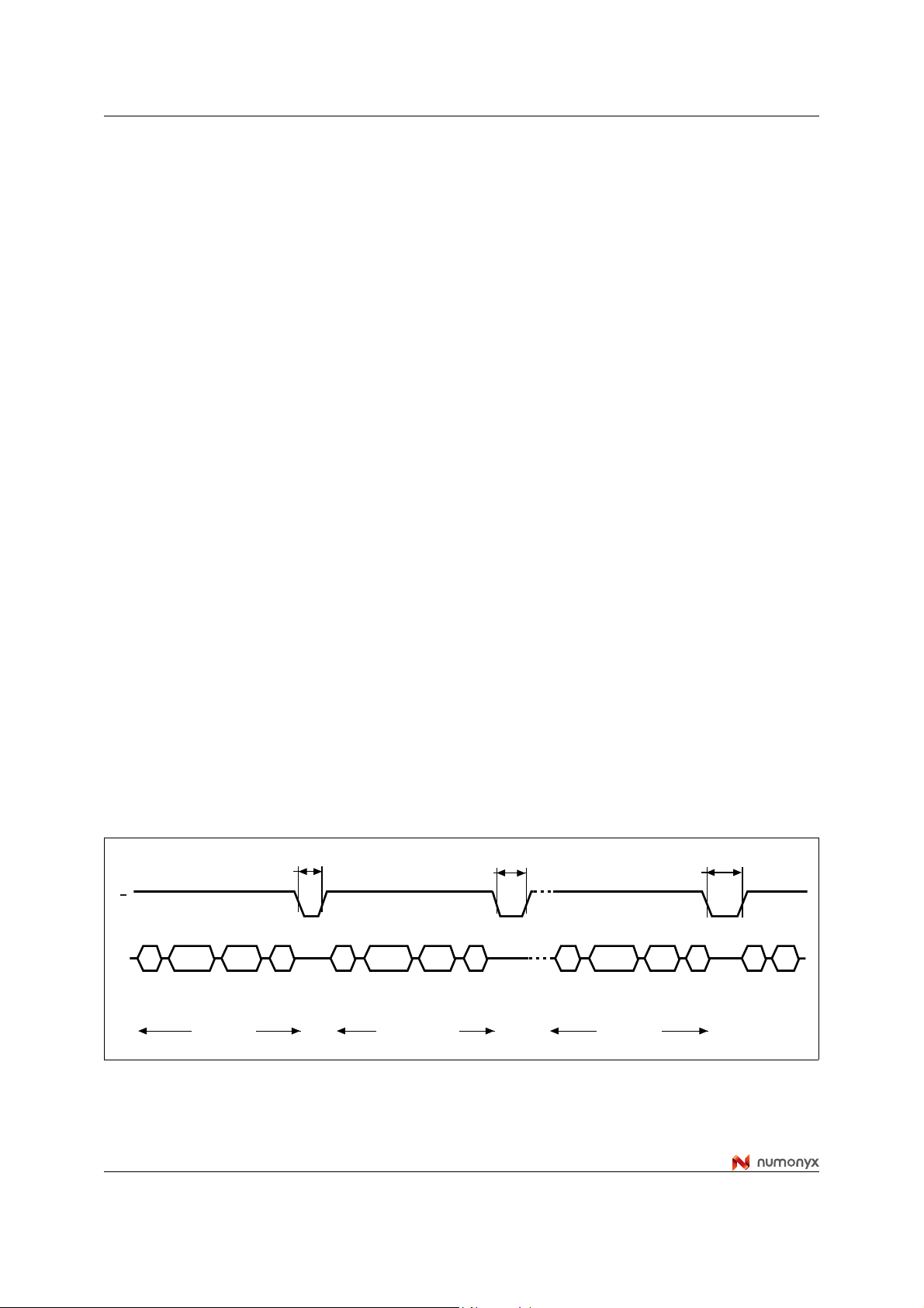
6.5 Cache program
The cache program operation is used to improve the programming throughput by
programming data using the ca che regi ster. The cache progr am op eratio n can only be used
within one block. The cache re gister allows ne w data to be input while the pre vious dat a that
was transferred to the page buffer is programmed into the memory array.
The following sequence is required to issue a cache program operation (refer to Figure 13):
1. First of all the program setup command is issued: one bus cycle to issue the program
setup command then 4 or 5 bus write cycles to input the address (see Table 6 and
Table 7). The data is then input (up to 2112 bytes/1056 words) and loaded into the
cache register
2. One bus cycle is required to issue the confirm command to start the P/E/R controller
3. The P/E/R controller then transfers the data to the page buffer . During this the de vice is
busy for a time of t
4. Once the data is loaded into the page buff er the P/E/R controller prog rams the data in to
the memory array. As soon as the cache registers are empty (after t
Cache Program command can be issued, while the internal programming is still
executing.
Once the program operation has started the status register can be read using the Read
Status Register command. During cache program operations SR5 can be read to find out
whether the internal programming is ongoing (SR5 = ‘0’) or has completed (SR5 = ‘1’) while
SR6 indicates whether the cache register is ready to accept new data. If any errors have
been detected on the previous page (P age N-1), the cache program error bit SR1 will be set
to ‘1', while if the error has been detected on page N the error bit SR0 will be set to '1’.
BLBH5
) a new
BLBH5
When the next page (Page N) of data is input with the Cache Pro gram command, t
affected by the pending internal programming. The data will only be transferred from the
cache register to the page buffer when the pending program cycle is finished and the page
buffer is available.
If the system monitors the progress of the operation using only the Ready/Busy signal, the
last page of data must be programmed with the Page Program Confirm command (10h).
If the Cache Program Confirm command (15h) is used inst ead, status reg iste r bit SR5 m ust
be polled to find out if the last programming is finished before starting any other operations.
Figure 13. Cache program operation
tBLBH5
(Cache Busy time)
RB
Busy
I/O
1. Up to 64 pages can be programmed in one cache program operation.
2. t
Address
80h
Inputs
Page
Program
Code
CACHEPG
+ Last page data loading time).
is the program time for the last page + the program time for the (last − 1)th page − (Program command cycle time
Data
Inputs
First Page
15h
Cache
Program
Code
Address
80h
Inputs
Page
Program
Code
Second Page
(can be repeated up to 63 times)
tBLBH5 tCACHEPG
Data
15h
Inputs
Cache Program
Confirm Code
Busy
Address
Inputs
Last Page
Data
Inputs
Page
Program
Confirm Code
Busy
BLBH5
SR070h80h 10h
Read Status
Register
ai08672
is
28/60
Page 29

NAND01G-B2B, NAND02G-B2C Device operations
6.6 Block erase
Erase operations are done one block at a time. An erase operation sets all of the bits in the
addressed block to ‘1’. All previous data in the block is lost.
An erase operation consists of three steps (refer to Figure 14):
1. One bus cycle is required to setup the Block Erase command. Only addresses A18-
A28 (x8) or A17-A27 (x16) are used, the other address inputs are ignored
2. Two or three b us cycles are then required to load the address of the block to be er ased.
Refer to Table 8 and Table 9 for the block addresses of each device
3. One bus cycle is required to issue the Block Erase Confirm command to start the P/E/R
controller.
The operation is initiated on the rising edge of write Enable, W
is issued. The P/E/R controller handles block erase and implements the verify process.
During the block erase operation, only the Read Status Register and Reset commands will
be accepted, all other commands will be ignored.
Once the program operatio n has co mpleted t he P/E/R co ntroller bit SR6 is set to ‘1’ and the
Ready/Busy signal goes High. If the operation completed successfully , the write status bit
SR0 is ‘0’, otherwise it is set to ‘1’.
Figure 14. Block erase operation
RB
I/O
60h
Block Erase
Setup Code
Block Address
Inputs
6.7 Reset
D0h
Confirm
Code
tBLBH3
(Erase Busy time)
Busy
, after the Confirm command
70h
Read Status Register
SR0
ai07593
The Reset command is used to reset the command interface and status register. If the
Reset command is issued during any operation, the operation will be aborted. If it was a
program or erase operation that was aborted, the contents of the memory locations being
modified will no longer be valid as the data will be partially programmed or erased.
If the device has already been reset then the new Reset command will not be accepted.
The Ready/Busy signal goes Low for t
of t
depends on the operation that the de vice w as p erf o rming when the command was
BLBH4
after the Reset command is issued. The value
BLBH4
issued, refer to Table 25: AC characteristics for operati ons for the values.
29/60
Page 30

Device operations NAND01G-B2B, NAND02G-B2C
6.8 Read status register
The device contains a status regist er which provides information on the current or previous
program or erase operation. The various bits in the status register convey information and
errors on the operation.
The status register is read by issuing the Read Status Register command. The status
register information is present on the output data bus (I/O0-I/O7) on the falling edge of Chip
Enable or Read Enable, whichever occu rs last. When several memories are connected in a
system, the use of Chip Enable and Read Enable signals allows the system to poll each
device separately, even when the Ready/Busy pins are common -wired. It is not necessary to
toggle the Chip Enable or Read Enable signals to update the contents of the status r egister.
After the Read Status Register command has been issued, the device remains in read
status register mode until another command is issued. Therefore if a Read Status Register
command is issued during a random read cycle a new Read command must be issued to
continue with a page read operation.
The Status Register bits are summarized in Table 13: Status register bits,. Ref er t o Table 13
in conjunction with the following text descriptions.
6.8.1 Write protection bit (SR7)
The write protection bit can be used to identify if the device is protected or not. If the write
protection bit is set to ‘1’ the device is not protected and program or erase operations are
allowed. If the write protection bit is set to ‘0’ the device is protected and program or erase
operations are not allowed.
6.8.2 P/E/R controller and cache ready/busy bit (SR6)
Status register bit SR6 has two different functions depending on the current operation.
During cache program operations SR6 acts as a cache program ready/busy bit, which
indicates whether the cache register is ready to acce pt new dat a. When SR6 is set to '0', the
cache register is busy and when SR6 is set to '1', the cache register is ready to accept new
data.
During all other operations SR6 acts as a P/E/R controlle r bit, which indicates whether the
P/E/R controller is active or inactive. When the P/E/R controller bit is set to ‘0’, the P/E/R
controller is active (device is busy); when the bit is set to ‘1’, the P/E/R controller is inactive
(device is ready).
6.8.3 P/E/R controller bit (SR5)
The program/erase/rea d controller bit indicates whether the P/E/R controller is active or
inactive. When the P/E/R controller bit is set to ‘0’, the P/E/R controller is active (device is
busy); when the bit is set to ‘1’, the P/E/R controller is inactive (device is ready).
30/60
Page 31

NAND01G-B2B, NAND02G-B2C Device operations
6.8.4 Cache program error bit (SR1)
The ca c h e progra m error bit can b e used to iden tify if th e previous page (page N-1) has been
successfully programmed or not in a cache program operation. SR1 is set to ’1’ when the
cache program operation has failed to program the pr evious page (page N-1) correctly. If
SR1 is set to ‘0’ the operation has completed successfully.
The cache program error bit is only valid during cache program operations, during other
operations it is don’t care.
6.8.5 Error bit (SR0)
The error bit is used to identify if any e rror s have been detected by the P/E/R controller. The
error bit is set to ’1’ when a program or e rase oper ation has failed to write the correct data to
the memory. If the error bit is set to ‘0’ the opera tion has completed successfully. The error
bit SR0, in a cache program operation, indicates a failure on page N.
6.8.6 SR4, SR3 and SR2 are reserved
Table 13. Status register bits
SR7 Write protection
SR6
SR5
SR4, SR3, SR2 Reserved
SR1
SR0
Bit Name Logic level Definition
'1' Not protected
'0' Protected
Program/ erase/ read
controller
Cache ready/busy
Program/ erase/ read
controller
Cache program error
Generic error
Cache program error
(1)
(2)
'1' P/E/R C inactive, device ready
'0' P/E/R C active, device busy
'1' Cache register ready (cache operation only)
'0' Cache register busy (cache operation only)
'1' P/E/R C inactive, device ready
'0' P/E/R C active, device busy
Don’t care
'1' Page N-1 failed in cache program operation
'0' Page N-1 programmed successfully
‘1’ Error – operation failed
‘0’ No Error – operation successful
‘1’ Page N failed in cache program operation
‘0’ Page N progra mmed successfully
1. Only valid for cache program operations, for other operations it is same as SR6.
2. Only valid for cache operations, for other operations it is don’t care.
31/60
Page 32

Device operations NAND01G-B2B, NAND02G-B2C
6.9 Read electronic signature
The dev ice contains a manufacturer code and device code. To read these codes three steps
are required:
1. One bus write cycle to issue the Read Electronic Signature command (90h)
2. One bus write cycle to input the address (00h)
3. Four bus read cycles to sequentially output the data (as shown in Table 14: Electronic
signature).
Table 14. Electronic signature
byte/word 1 byte/word 2
Part number
NAND01GR3B2B
Manufacturer
code
Device code
A1h
byte/word 3
(see Table 15)
byte/word 4
(see Table 16)
15h
20h
NAND01GW3B2B F1h 1Dh
NAND01GR4B2B
B1h 55h
0020h
NAND01GW4B2B C1h 5Dh
80h
NAND02GR3B2C
AAh 15h
20h
NAND02GW3B2C DAh 1Dh
NAND02GR4B2C
BAh 55h
0020h
NAND02GW42C CAh 5Dh
Table 15. Electronic signature byte 3
I/O Definition Value Description
I/O1-I/O0 Internal chip number
I/O3-I/O2 Cell type
0 0
0 1
1 0
1 1
0 0
0 1
1 0
1 1
1
2
4
8
2-level cell
4-level cell
8-level cell
16-level cell
I/O5-I/O4
I/O6
Number of simultaneously
programmed pages
Interleaved programming
between multiple devices
I/O7 Cache program
32/60
0 0
0 1
1 0
1 1
0
1
0
1
1
2
4
8
Not supported
supported
Not supported
supported
Page 33

NAND01G-B2B, NAND02G-B2C Device operations
Table 16. Electronic signature byte/word 4
I/O Definition Value Description
I/O1-I/O0
I/O2
I/O7, I/O3
I/O5-I/O4
Page size
(without spare area)
Spare area size
(byte / 512-byte)
Minimum sequential
access time
Block size
(without spare area)
I/O6 Organization
0 0
0 1
1 0
1 1
0
1
0 0
0 1
1 0
1 1
0 0
0 1
1 0
1 1
0
1
1Kbyte
2Kbytes
Reserved
Reserved
8
16
50 ns
30 ns
25 ns
Reserved
64 Kbytes
128 Kbytes
256 Kbytes
Reserved
X8
X16
33/60
Page 34

Data protection NAND01G-B2B, NAND02G-B2C
7 Data protection
The device has hardware features to protect against program and erase operations.
It features a Write Protect, WP
and erase operations. It is recommended to keep WP
down.
In addition, to protect the memory from any involuntary program/erase operations during
power-transitions, the device has an internal voltage detector which disables all functions
whenever V
is below V
DD
, pin, which can be used to protect the de vice against prog ram
at VIL during power-up and power-
(see Table 22 and Table 23).
LKO
34/60
Page 35

NAND01G-B2B, NAND02G-B2C Software algorithms
8 Software algorithms
This section gives information on the software algorithms that Numonyx recommends to
implement to manage the bad blocks and extend the lifetime of the NAND device.
NAND flash memories are programmed and erased by Fowler-Nordheim tunneling using a
high voltage. Exposing the device to a high voltage for extended periods can cause the
oxide layer to be damaged. For this reason, the number of program and erase cycles is
limited (see Table 18 for value) and it is recommended to implement garbage collection, a
wear-leveling algorithm and an error correction code, to extend the number of program and
erase cycles and increase the data retention.
To help integrate a NAND memory into an application, Numonyx can provide a file system
OS native reference software, which supports the basic commands of file management.
Contact the nearest Numonyx sales office for more details.
8.1 Bad block management
Devices with bad blocks have the same quality level and the same AC and DC
characteristics as devices where all the blocks are valid. A bad block does not affect the
performance of valid blocks because it is isolated from the bit line and common source lin e
by a select transistor.
The devices are supplied with all the locations inside valid blocks erased (FFh). The bad
block information is written prior to shipping. Any block, where the 1st and 6th bytes, or 1st
word, in the spare area of the 1st page, does not contain FFh, is a bad block.
The bad block Information must be read before any erase is attempted as the bad block
information may be er ased . For the system to be able to r ecogniz e the bad blocks based on
the original information it is recommended to create a bad b lock t able f o llowing the flo wchart
shown in Figure 15.
8.2 NAND flash memory failure modes
Over the lifetime of the device additional bad blocks may develop.
To implement a highly reliable system, all the possible failure modes must be considered:
● Program/er ase failure: in t his case the bloc k has to be re placed by co pying the data to
a valid block. These additional bad blocks can be identified as attempts to progr am or
erase them will give errors in the status register
As the failure of a page progr am operation does not aff ect the da ta in other pages in the
same block, the b loc k can be replaced b y re-prog ramming the current data and cop ying
the rest of the replaced block to an available valid block. The Copy Back Program
command can be used to copy the data to a valid block. See Section 6.4: Copy back
program for more details
● Read failure: in this case, ECC correction m ust be imp leme nted . To efficiently use the
memory space, it is recommended to recover single-bit error in read by ECC, without
replacing the whole block.
Refer to Table 17 for the procedure to follow if an error occurs during an operation.
35/60
Page 36

Software algorithms NAND01G-B2B, NAND02G-B2C
Table 17. NAND flash failure modes
Operation Procedure
Erase Block replacement
Program Block replacement or ECC
Read ECC
Figure 15. Bad block management flowchart
START
Block Address =
Block 0
Increment
Block Address
Figure 16. Garbage collection
Old area
Valid
page
Invalid
page
Data
= FFh?
YES
Last
block?
YES
END
NO
NO
(erased)
Free
page
Update
Bad Block table
AI07588C
New area (after GC)
36/60
AI07599B
Page 37

NAND01G-B2B, NAND02G-B2C Software algorithms
8.3 Garbage collection
When a data page needs to be modified, it is faster to write to the first available page, and
the previous page is marked as invalid. After several updates it is necessary to remove
invalid pages to free some memory space.
To free this memory space and allow further program operations it is recommended to
implement a garbage collection algorithm. In a garbage collection software the valid pages
are copied into a free area and the block containing the invalid pages is erased (see
Figure 16).
8.4 Wear-leveling algorithm
For write-intensive applications, it is recommended to implement a wear-leveling algorithm
to monitor and spread the number of write cycles per block.
In memories that do not use a wear-leveling algorithm not all blocks get used at the same
rate. Blocks with long-lived data do not endure as many write cycles as the blocks with
frequently-changed data.
The wear-leveling algorithm ensures that equal use is made of all the available write cycles
for each block. There are two wear-leveling levels:
● First level wear-leveling, new data is programmed to the free blocks that have had the
fewest write cycles
● Second level wear-leveling, long-lived data is copied to another block so that the
original block can be used for more frequently-changed data.
The second lev el wear-leveling is triggered when the difference between the maximum and
the minimum number of write cycles per block reaches a specific threshold.
8.5 Error correction code
An error correction code (ECC) can be implemented in the NAND flash memories to identify
and correct errors in the data.
For e v ery 2048 bits in the de vice it is recommended to implement 2 2 bits of ECC (16 b its for
line parity plus 6 bits for column parity).
An ECC model is available in VHDL or Verilog. Contact the nearest Numon yx sales office f or
more details.
37/60
Page 38

Software algorithms NAND01G-B2B, NAND02G-B2C
Figure 17. Error detection
New ECC generated
during read
XOR previous ECC
with new ECC
All results
= zero?
YES
22 bit data = 0
No Error
8.6 Hardware simulation models
8.6.1 Behavioral simulation models
Denali Software Corporation models are platform independent functional models designed
to assist customers in performing entire system simulations (typical VHDL/Verilog). These
models describe the logic behavior and timings of NAND flash devices, and so allow
software to be developed before hardware.
8.6.2 IBIS simulations models
>1 bit
= zero?
YES
11 bit data = 1NO1 bit data = 1
Correctable
Error
NO
ECC Error
ai08332
IBIS (I/O buffer information specification) models describe the behavior of the I/O buffers
and electrical characteristics of flash devices.
These models provide information such as AC characteristics, rise/fall times and package
mechanical data, all of which are measured or simulated at v oltage an d temper ature ran ges
wider than those allowed by target specifications.
IBIS models are used to simulate PCB connections and can be used to resolve compatibility
issues when upgrading devices. They can be imported into SPICETOOLS.
38/60
Page 39

NAND01G-B2B, NAND02G-B2C Program and erase times and endurance cycles
9 Program and erase times and endurance cycles
The program and erase t imes and the n umber of prog ram/ erase cycle s per b loc k ar e show n
in Table 18.
Table 18. Program, erase times and program erase endurance cycles
NAND flash
Parameters
Min Typ Max
Page program time 200 700 µs
Block erase time
Program/erase cycles per block (with ECC) 100 000 cycles
Data retention 10 years
2 3ms
Unit
39/60
Page 40

Maximum ratings NAND01G-B2B, NAND02G-B2C
10 Maximum ratings
Stressing the device above the ratings listed in Table 19: Absolute maximum ratings, may
cause permanent damage to the device. These are stress ratings only and operation of the
device at these or any other conditions above those indicated in the operating sections of
this specification is not implied. Exposure to absolute maximum rating conditions for
extended periods may aff ect device reliability.
Table 19. Absolute maximum ratings
Value
Symbol Parameter
Min Max
Unit
T
BIAS
T
STG
(1)
V
IO
V
DD
1. Minimum voltage may undershoot to –2V for less than 20 ns during transitions on input and I/O pins.
Maximum voltage may overshoot to VDD + 2 V for less than 20 ns during transitions on I/O pins.
Temperature under bias – 50 125 °C
Storage temperature – 65 150 °C
1.8 V devices – 0.6 2.7 V
Input or output voltage
3 V devices – 0.6 4.6 V
1.8 V devices – 0.6 2.7 V
Supply voltage
3 V devices – 0.6 4.6 V
40/60
Page 41

NAND01G-B2B, NAND02G-B2C DC and AC parameters
11 DC and AC parameters
This section summarizes the operating and measurement conditions, and the DC and AC
characteristics of the device. The parameters in the DC and AC characteristics tables that
follow, are derived from tests performed under the measurement conditions summariz ed in
Table 20: Operating and AC measurement conditions. Designers should check that the
operating conditions in their circuit match the measurement conditions when relying on the
quoted parameters.
Table 20. Operating and AC measurement conditions
NAND flash
Parameter
Min Max
Units
1.8 V devices 1.7 1.95 V
Supply voltage (V
DD
)
3 V devices 2.7 3.6 V
Grade 1 0 70 °C
Ambient temperature (TA)
Grade 6 –40 85 °C
Load capacitance (C
(1 TTL GATE and C
Input pulses voltages
)
L
)
L
1.8 V devices 30 pF
3 V devices (2.7 - 3.6 V) 50 pF
1.8 V devices 0 V
DD
3 V devices 0.4 2.4 V
Input and output timing ref. voltages VDD/2 V
Output circuit resistor R
8.35 kΩ
ref
Input rise and fall times 5 ns
Table 21. Capacitance
(1)
Symbol Parameter Test condition Typ Max Unit
C
C
I/O
= 25 °C, f = 1 MHz. CIN and C
1. T
A
2. Input/output capacitances double in stacked devices.
Input capacitance VIN = 0 V 10 pF
IN
Input/output capacitance
(2)
are not 100% tested.
I/O
VIL = 0 V 10 pF
V
41/60
Page 42
DC and AC parameters NAND01G-B2B, NAND02G-B2C
Figure 18. Equivalent testing circuit for AC characteristics mea surement
V
DD
2R
ref
NAND flash
C
L
2R
ref
GND
GND
Ai11085
42/60
Page 43

NAND01G-B2B, NAND02G-B2C DC and AC parameters
Table 22. DC characteristics, 1.8 V devices
Symbol Parameter Test conditions Min Typ Max Unit
I
DD1
I
DD2
I
DD3
I
DD5
I
V
V
V
V
I
LO
LI
IH
OH
OL
Operating current
Standby current (CMOS)
Input leakage current
Output leakage current
Input high voltage – VDD-0.4 – VDD+0.3 V
IL
Input low voltage – -0.3 – 0.4 V
Output high voltage level IOH = –100 µA VDD-0.1 – – V
Output low voltage level IOL = 100 µA – – 0.1 V
Sequential
read
Program – - 8 15 mA
Erase – - 8 15 mA
(1)
(1)
(1)
IOL (RB) Output low current (RB) V
V
LKO
1. Leakage current and standby current double in stacked devices.
Table 23. DC characteristics, 3 V devices
VDD supply voltage (erase and
program lockout)
t
minimum
RLRL
E = V
IL, IOUT
E = VDD – 0.2,
WP = 0/V
= 0 mA
DD
-815mA
- 10 50 µA
VIN = 0 to VDDmax - – ±10 µA
V
= 0 to VDDmax - – ±10 µA
OUT
= 0.1 V 3 4 mA
OL
– – – 1.1 V
Symbol Parameter Test conditions Min Typ Max Unit
I
DD1
I
DD2
I
DD3
I
DD4
I
DD5
I
V
V
V
V
I
LI
LO
OH
OL
Sequential
Read
Operating current
Program – –1020mA
Erase – –1020mA
Standby current (TTL)
Standby current (CMOS)
Input leakage current
Output leakage current
IH
IL
Input high voltage – 0.8V
Input low voltage – -0.3 – 0.2V
(1)
(1)
(1)
(1)
Output high voltage level IOH=–400µA 2.4 – – V
Output low voltage level IOL=2.1mA – – 0.4 V
t
minimum
RLRL
E =V
IL, IOUT
=0mA
E =VIH, WP =0/V
E = V
W
DD
P = 0/V
– 0.2,
DD
DD
–1020mA
1 mA
– 10 50 µA
VIN = 0 to VDDmax – – ±10 µA
V
= 0 to VDDmax – – ±10 µA
OUT
DD
– VDD+0.3 V
DD
IOL (RB) Output low current (RB) VOL=0.4V 8 10 mA
V
LKO
1. Leakage current and standby current double in stacked devices.
VDD supply voltage (erase and
program lockout)
– – – 1.7 V
V
43/60
Page 44
DC and AC parameters NAND01G-B2B, NAND02G-B2C
Table 24. AC characteristics for command, address, data input
Symbol
t
ALLWH
t
ALHWH
t
CLHWH
t
CLLWH
t
DVWH
t
ELWH
t
WHALH
t
WHALL
t
WHCLH
t
WHCLL
t
WHDX
t
WHEH
t
WHWL
t
WLWH
t
WLWL
Alt.
symbol
t
ALS
t
CLS
t
DS
t
CS
t
ALH
t
CLH
t
DH
t
CH
t
WH
t
WP
t
WC
Parameter
Address Latch Low to Write Enab le Hi g h
AL setup time Min 25 15 ns
Address Latch High to Write Enable High
Command Latch High to Write Enable
High
CL setup time Min 25 15 ns
Command Latch Low to Write Enable
High
Data Valid to Write Enable High Data setup time Min 20 15 ns
Chip Enable Low to Write Enable High E setup time Min 35 20 ns
Write Enable High to Address Latch High AL hold time Min
Write Enable High to Address Latch Low AL hold time Min
Write Enable High to Command Latch
High
CL hold time Min 10 5 ns
Write Enable High to Command Latch
Low
Write Enable High to Data Transition Data hold time Min 10 5 ns
Write Enable High to Chip Enable High E hold time Min 10 5 ns
Write Enable High to Write Enable Low W High hold time Min 15 10 ns
Write Enable Low to Write Enable High W pulse width Min 25 15 ns
Write Enable Low to Write Enable Low Write cycle time Min 45 30 ns
1.8 V
devices
3 V
devices
10 5 ns
Unit
44/60
Page 45
NAND01G-B2B, NAND02G-B2C DC and AC parameters
Table 25. AC characteristics for operations
Symbol
t
ALLRL1
t
ALLRL2
t
BHRL
t
BLBH1
t
BLBH2
t
BLBH3
Alt.
symbol
t
AR
t
RR
t
PROG
t
BERS
Address Latch Low to
Read Enable Lo w
Read electronic signature Min 10 10 ns
Read cycle Min 10 10 ns
Ready/Busy High to Read Enable Low Min 20 20 ns
Read busy time Max 25 25 µs
Program busy time Max 700 700 µs
Erase busy time Max 3 3 ms
(1)
Parameter
1.8 V
devices
3 V
devices
Reset busy time, during ready Max 5 5 µs
t
BLBH4
t
RST
Ready/Busy Low to
Ready/Busy High
Reset busy time, during read Max 5 5 µs
Reset busy time, during program Max 10 10 µs
Reset busy time, during erase Max 500 500 µs
t
BLBH5
t
CLLRL
t
DZRL
t
EHQZ
t
RHQZ
t
WHWHtADL
t
VHWH
t
VLWH
t
ELQV
t
RHRL
t
EHQX
t
RHQX
t
RLRH
t
RLRL
t
RLQV
t
WHBH
t
WHBL
t
WHRL
1. The time to ready depends on the value of the pull-up resistor tied to the ready/busy pin. See Figure 31, Figure 32 and
Figure 33.
2. t
WHWH
3. During a program/erase enable operation, t
During a program/erase disable Operation, t
4. ES = electronic signature.
t
CBSY
t
CLR
t
IR
t
CHZ
t
RHZ
Command Latch Low to Read Enable Low Min 10 10 ns
Data Hi-Z to Read Enable Low Min 0 0 ns
Chip Enable High to Output Hi-Z Max 30 30 ns
Read Enable High to Output Hi-z Max 30 30 ns
Last address latched to data loading time during program
(2)
Cache busy time
operations
(3)
t
WW
t
t
T
t
t
t
WHR
is the time from W rising edge during the final address cycle to W rising edge during the first data cycle.
Write protection time Min 100 100 ns
Chip Enable Low to Output Valid Max 45 25 ns
CEA
Read Enable High to
REH
Read Enable Lo w
Chip Enable High or Read Enable high to Output Hold Min 10 10 ns
OH
Read Enable Lo w t o
t
RP
Read Enable High
Read Enable Lo w t o
t
RC
Read Enable Lo w
Read Enable Lo w t o
REA
Output Valid
Write Enable High to
t
R
Ready/Busy High
Write Enable High to Ready/Busy Low Max 100 100 ns
WB
Read Enable High hold time Min 15 10 ns
Read Enable pulse width Min 25 15 ns
Read cycle time Min 50 30 ns
Read Enable access time
Read ES access time
(4)
Read busy time Max 25 25 µs
Write Enable High to Read Enable Low Min 60 60 ns
is the delay from WP high to W High.
WW
is the delay from WP Low to W High.
WW
Typ 3 3 µs
Max 700 700 µs
Min 100 100 ns
Max 30 20 ns
Unit
45/60
Page 46

DC and AC parameters NAND01G-B2B, NAND02G-B2C
Figure 19. Command latch AC waveforms
CL
tCLHWH
(CL Setup time) (CL Hold time)
tELWH
H(E Setup time)
E
W
tALLWH tWHALH
(ALSetup time) (AL Hold time)
AL
tDVWH tWHDX
(Data Setup time) (Data Hold time)
I/O
Figure 20. Address latch AC waveforms
tCLLWH
(CL Setup time)
CL
tWLWH
Command
tWHCLL
tWHEH
(E Hold time)
ai13105
tELWH
(E Setup time)
tWLWL
E
tWLWH
W
tALHWH
(AL Setup time)
tWHWL
tWHALL
(AL Hold time)
tWHWL
tWHALL
AL
tDVWH
tWHDX
(Data Hold time)
Adrress
cycle 2
I/O
tDVWH
(Data Setup time)
Adrress
cycle 1
1. A fifth address cycle is required for 2-Gbit devices only.
tWLWL tWLWL
tWHWL
tWHALL
tDVWH
tWHDX
Adrress
cycle 3
tWLWHtWLWH tWLWH
tDVWH
tWHDX
tWHWL
tWHALL
Adrress
cycle 4
tWLWL
tWLWH
tDVWH
tWHDX
Adrress
cycle 5
tWHDX
ai13106
46/60
Page 47
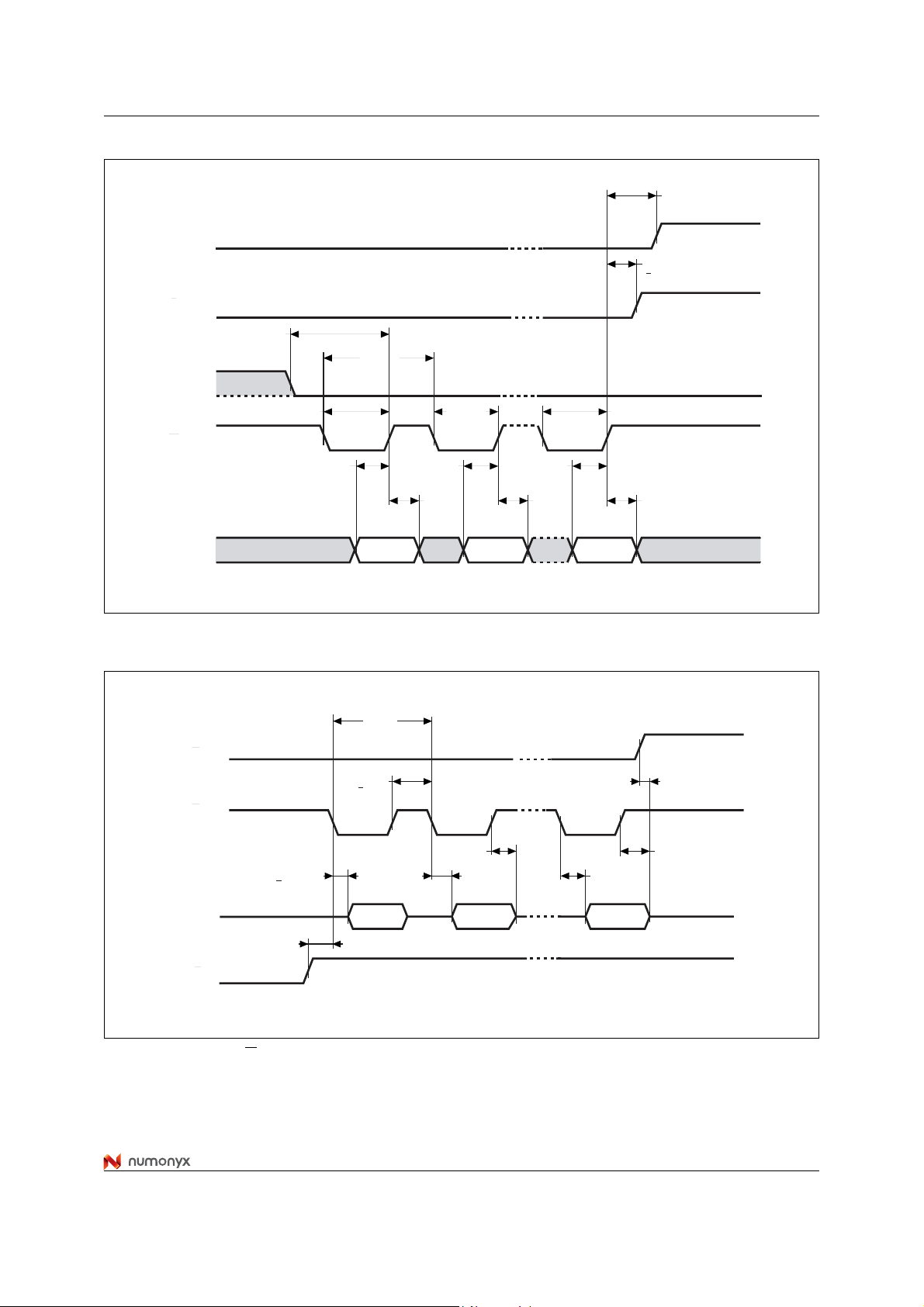
NAND01G-B2B, NAND02G-B2C DC and AC parameters
Figure 21. Data Input Latch AC waveforms
tWHCLH
(CL Hold time)
CL
tWHEH
(E Hold time)
E
tALLWH
(ALSetup time)
AL
tWLWL
tWLWH
tWLWH
W
I/O
tDVWH
(Data Setup time)
Data In 0 Data In 1
tDVWH
tWHDX
(Data Hold time)
tDVWH
1. Data in last is 2112 in x8 devices and 1056 in x16 devices.
Figure 22. Sequential data output after read AC waveforms
tRLRL
(Read Cycle time)
E
tRHRL
(R High Holdtime)
R
tRHQZ
tRLQV
(R Accesstime)
tRLQV
tWHDX
Data In
Last
tEHQZ
tRLQV
tWLWH
tWHDX
ai13107
tRHQZ
I/O
tBHRL
RB
1. CL = Low, AL = Low, W = High.
Data Out Data Out Data Out
ai08031
47/60
Page 48

DC and AC parameters NAND01G-B2B, NAND02G-B2C
Figure 23. Read status register AC waveforms
tCLLRL
CL
tWHCLL
tCLHWH
tWHEH
E
tELWH
tWLWH
W
R
tDZRL
I/O
tDVWH
(Data Setup time)
70h
tWHDX
(Data Hold time)
Figure 24. Read electronic signature AC waveforms
CL
tWHRL
tELQV
tRLQV
tEHQZ
tRHQZ
Status Register
Output
ai13108
E
W
AL
tALLRL1
R
tRLQV
(Read ES Access time)
I/O
1. Refer to Table 14 for the values of the manufacturer and device codes, and to Table 15 and Table 16 for the information
contained in byte 3 and 4.
90h 00h
Read Electronic
Signature
Command
1st Cycle
Address
Man.
code
Device
code
Byte3Byte1 Byte2
00h
Byte4
see Note.1
ai08667
48/60
Page 49

NAND01G-B2B, NAND02G-B2C DC and AC parameters
Figure 25. Page read operation AC waveforms
CL
E
RB
AL
tWLWL
W
tWHBL
tALLRL2
tWHBH tRLRL
(Read Cycle time)
R
tRLRH
tBLBH1
tEHQZ
tRHQZ
I/O
00h
Command
Add.N
Add.N
cycle 1
cycle 2
Address N Input
Add.N
cycle 3
Add.N
cycle 4
Add.N
cycle 5
Code
1. A fifth address cycle is required for 2-Gbit devices only.
30h
DataNData
N+1
Data
N+2
Data Output
Busy
from Address N to Last Byte or Word in Page
Data
Last
ai13109b
49/60
Page 50

DC and AC parameters NAND01G-B2B, NAND02G-B2C
Figure 26. Page program AC waveforms
CL
E
tWLWL tWLWL tWLWL
(Write Cycle time)
W
AL
R
I/O
RB
80h
Page Program
Setup Code
Add.N
cycle 1
Add.N
cycle 2
cycle 3
Add.N
Add.N
cycle 4
Address Input Data Input
1. A fifth address cycle is required for 2-Gbit devices only.
Add.N
cycle 5
tWHWH
N
tWHBL
tBLBH2
(Program Busy time)
Last
10h
Confirm
Code
Page
Program
SR0
70h
Read Status Register
ai13110b
50/60
Page 51

NAND01G-B2B, NAND02G-B2C DC and AC parameters
Figure 27. Block erase AC waveforms
CL
E
tWLWL
(Write Cycle time)
W
tWHBL
AL
R
Add.
Add.
I/O
RB
Block Erase
Setup Command
cycle 1
cycle 2
Block Address Input
Add.
cycle 3
1. Address cycle 3 is required for 2-Gbit devices only.
Figure 28. Reset AC waveforms
W
AL
D0h60h
Confirm
Code
tBLBH3
(Erase Busy time)
Block Erase
70h
Read Status Register
SR0
ai08038b
I/O
RB
CL
R
FFh
tBLBH4
(Reset Busy time)
51/60
ai08043
Page 52

DC and AC parameters NAND01G-B2B, NAND02G-B2C
Figure 29. Program/erase enable waveforms
W
tVHWH
WP
RB
I/O
80h 10h
Figure 30. Program/erase disable waveforms
W
tVLWH
WP
High
RB
I/O
80h 10h
11.1 Ready/Busy signal electrical characteristics
Figure 32, Figure 31 and Figure 33 show the electrical characteristics for the Ready/Busy
signal. The value required f o r the resistor R
RPmin
can be calculated using the following equation:
P
V
DDmaxVOLmax
-------------------------------------------------------------=
–()
I
+
I
OL
L
ai12477
ai12478
So,
RPmin 1.8V()
RPmin 3V()
where I
is the sum of the input currents of all the devices tied to the Ready/Busy signal. RP
L
max is determined by the maximum value of t
52/60
1.85V
---------------------------=
+
3mA I
3.2V
---------------------------=
+
8mA I
.
r
L
L
Page 53
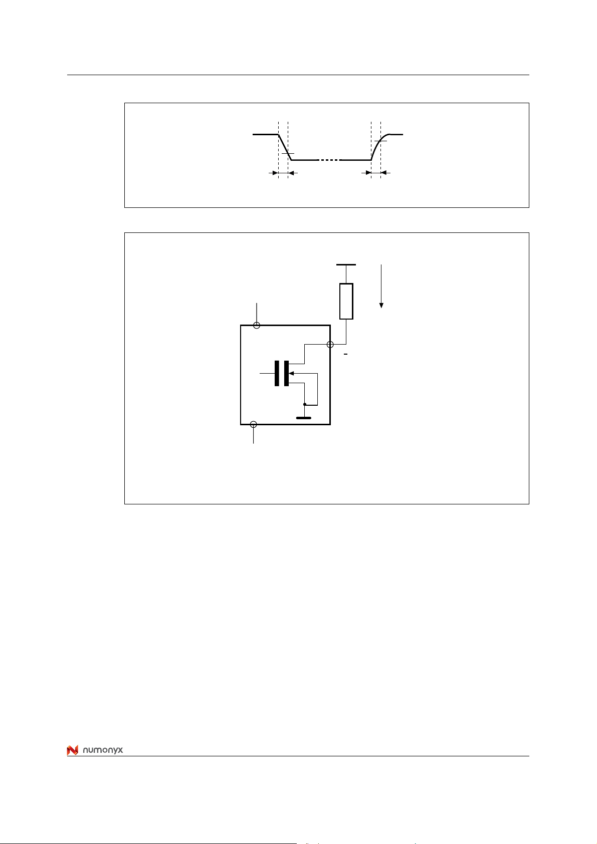
NAND01G-B2B, NAND02G-B2C DC and AC parameters
Figure 31. Ready/Busy AC waveform
ready V
DD
V
V
OL
busy
t
f
OH
t
r
AI07564B
Figure 32. Ready/Busy load circuit
V
DD
DEVICE
V
SS
R
P
RB
Open Drain Output
ibusy
AI07563B
53/60
Page 54

DC and AC parameters NAND01G-B2B, NAND02G-B2C
Figure 33. Resistor value versus waveform timings for Ready/Busy signal
VDD = 1.8V, CL = 30pF VDD = 3.3V, CL = 100pF
400
300
(ns)
f
200
, t
1.7
r
t
100
30
1.7
0
1234
0.85
60
1.7
RP (KΩ)
90
0.57
1.7
1. T = 25°C.
11.2 Data protection
The Numonyx NAND device is designed to guarantee data protection during power
transitions.
A V
detection circuit disables all NAND operations, if VDD is below the V
DD
In the V
low (V
figure.
range from V
DD
) to guarantee hardware protection during power transitions as shown in the below
IL
4
3
(mA)
2
ibusy
120
1
0.43
1.7
t
f
to the lower limit of nominal range, the WP pin should be kept
LKO
400
300
2.4
(ns)
f
200
, t
r
t
100
100
3.6
0
1234
t
r
ibusy
200
1.2
3.6
RP (KΩ)
300
0.8
3.6
LKO
400
2
1
3.6
threshold.
4
3
0.6
(mA)
ibusy
ai07565B
Figure 34. Data protection
DD
W
Nominal Range
V
LKO
Locked
V
54/60
Locked
Ai11086
Page 55

NAND01G-B2B, NAND02G-B2C Package mechanical
12 Package mechanical
In order to meet environmen tal requir ements , Numon yx offers these de vices in ECOPACK®
packages. ECOPACK® packages are lead-free. The category of second level interconnect
is marked on the package and on the inner box label, in compliance with JEDEC Standard
JESD97. The maximum ratings related to soldering conditions are also marked on the inner
box label.
Figure 35. TSOP48 - 48 lead plastic thin small outl ine, 12 x 20 mm, package outline
1
D1
24
E1
E
DIE
1. Drawing is not to scale.
Table 26. TSOP48 - 48 lead plastic thin small outline, 12 x 20 mm, package mechanical data
48
e
B
25
A2
C
CP
L1
A
LA1 α
TSOP-G
millimeters inches
Symbol
Typ Min Max Typ Min Max
A 1.20 0.047
A1 0.10 0.05 0.15 0.004 0.002 0.006
A2 1.00 0.95 1.05 0.039 0.037 0.041
B 0.22 0.17 0.27 0.009 0.007 0.011
C 0.10 0.21 0.004 0.008
CP 0.08 0.003
D1 12.00 11.90 12.10 0.472 0.468 0.476
E 20.00 19.80 20.20 0.787 0.779 0.795
E1 18.40 18.30 18.50 0.724 0.720 0.728
e0.50– –0.020–
L 0.60 0.50 0.70 0.024 0.020 0.028
L1 0.80 0.031
α 3° 0° 5° 3° 0° 5°
55/60
Page 56

Package mechanical NAND01G-B2B, NAND02G-B2C
Figure 36. VFBGA63 9.5 x 12 mm - 6 x 8 active ball array, 0.80 mm pitch, package outline
D
D2
FD1
FD
D1
SD
e
E
e
E2
E1
BALL "A1"
eb
A
FE1
SE
FE
A2
A1
ddd
BGA-Z67
1. Drawing is not to scale
Table 27. VFBGA63 9.5 x 12 mm - 6 x 8 ball array, 0.80 mm pitch, package mechanical data
millimeters inches
Symbol
Typ Min Max Typ Min Max
A 1.05 0.041
A1 0.25 0.010
A2 0.70 0.028
b 0.45 0.40 0.50 0.018 0.016 0.020
D 9.50 9.40 9.60 0.374 0.370 0.378
D1 4.00 0.157
D2 7.20 0.283
ddd 0.10 0.004
E 12.00 11.90 12.10 0.472 0.468 0.476
E1 5.60 0.220
E2 8.80 0.346
e0.80– –0.031– –
FD 2.75 0.108
FD1 1.15 0.045
FE 3.20 0.126
FE1 1.60 0.063
SD 0.40 0.016
SE 0.40 0.016
56/60
Page 57

NAND01G-B2B, NAND02G-B2C Package mechanical
Figure 37. VFBGA63 9 x 11 mm - 6 x 8 active ball array, 0.80 mm pitch, package outline
D
D2
FD1
FE
e
E
E2 E1
BALL "A1"
A
eD1SD FD
SE
b
FE1
A2
A1
BGA-Z75
ddd
1. Drawing is not to scale
Table 28. VFBGA63 9 x 11 mm - 6 x 8 active ball array, 0.80 mm pitch, package mechanical data
millimeters inches
Symbol
Typ Min Max Typ Min Max
A 1.05 0.041
A1 0.25 0.010
A2 0.70 0.028
b 0.45 0.40 0.50 0.018 0.016 0.020
D 9.00 8.90 9.10 0.354 0.350 0.358
D1 4.00 0.157
D2 7.20 0.283
ddd 0.10 0.004
E 11.00 10.90 11.10 0.433 0.429 0.437
E1 5.60 0.220
E2 8.80 0.346
e 0.80 – – 0.031 – –
FD 2.50 0.098
FD1 0.90 0.035
FE 2.70 0.106
FE1 1.10 0.043
SD 0.40 – – 0.016 – –
SE 0.40 – – 0.016 – –
57/60
Page 58

Ordering information NAND01G-B2B, NAND02G-B2C
13 Ordering information
Table 29. Ordering information scheme
Example: NAND02GR3B2C ZA 6 E
Device type
NAND flash memory
Density
01G = 1 Gbit
02G = 2 Gbits
Operating voltage
R = V
W = V
Bus width
3 = x8
4 = x16
= 1.7 to 1.95 V
DD
= 2.7 to 3.6 V
DD
(1)
Family identifier
B = 2112-byte/ 1056-word page
Device options
2 = chip enable don't care enabled
Product version
B = second version (1-Gbit devices)
C = third version (2-Gbit devices)
Package
N = TSOP48 12 x 20 mm
ZA = VFBGA63 9.5 x 12 x 1 mm, 0.8 mm pitch
ZA= VFBGA63 9 x 11 x 1 mm, 0.8 mm pitch
(3)
Temperature range
1 = 0 to 70 °C
6 = –40 to 85 °C
Option
E = ECOPACK® package, standard packing
F = ECOPACK® package, tape & reel packing
1. x16 organization only available for MCP products.
2. For NAND02G-B2C devices only.
3. For NAND01G-B2B devices only.
(2)
Note: Devices are shipped from the factory with the memory content bits , in v alid b locks , erased to
’1’. For further information on any aspect of this device, please contact yo ur nearest
Numonyx sales office.
58/60
Page 59

NAND01G-B2B, NAND02G-B2C Revision history
14 Revision history
Table 30. Document revision history
Date Version Changes
18-May-2006 0.1 Initial release.
01-Jun-2006 1 Document status changed to preliminary data.
09-Jun-2006 2
23-Nov-2006 3
20-Apr-2007 4
14-Apr-2008 5 Applied Numonyx branding.
VFBGA63 9 x 11 x 1 mm package added for NAND01G-B2B devices
and VFBGA63 9.5 x 12 x 1 mm dedicated to NAND02G-B2C devices.
Note 2 below Commands removed.
Overview of Section 6.1: Read memory array updated. Paragraph
concerning Exit Cache Read command updated in Section 6.2: Cache
read. Block replacement section replaced by Section 8.2: NAND flash
memory failure modes.
added in Table 24: AC characteristics for command, address,
t
WHALL
data input.
wavef orm updated in Figure 25: Page read operation AC
RB
waveforms, and CL waveform modified in Figure 26: Page program AC
waveforms.
An error correction code (ECC) is required to obtain a data integrity of
100 000 program/erase cycles per bloc k.
Section 3.9: Ready/Busy (RB) modified.
timing removed from Figure 9: Page program operation and
t
RHRL2
Table 25: AC characteristics for operations.
Note removed below Figure 11: Copy back program.
t
WHBH2
replaced by t
, cash busy time, in Section 6.5: Cache
BLBH5
program.
is t
Alt. symbol for t
BLBH4
in Table25: AC characteristics f or
RST
operations.
59/60
Page 60

NAND01G-B2B, NAND02G-B2C
Please Read Carefully:
INFORMATION IN THIS DOCUMENT IS PROVIDED IN CONNECTION WITH NUMONYX™ PRODUCTS. NO LICENSE, EXPRESS OR
IMPLIED, BY ESTOPPEL OR OTHERWISE, TO ANY INTELLECTUAL PROPERTY RIGHTS IS GRANTED BY THIS DOCUMENT. EXCEPT
AS PROVIDED IN NUMONYX'S TERMS AND CONDITIONS OF SALE FOR SUCH PRODUCTS, NUMONYX ASSUMES NO LIABILITY
WHATSOEVER, AND NUMONYX DISCLAIMS ANY EXPRESS OR IMPLIED WARRANTY, RELATING TO SALE AND/OR USE OF
NUMONYX PRODUCTS INCLUDING LIABILITY OR WARRANTIES RELATING TO FITNESS FOR A PARTICULAR PURPOSE,
MERCHANTABILITY, OR INFRINGEMENT OF ANY PATENT, COPYRIGHT OR OTHER INTELLECTUAL PROPERTY RIGHT.
Numonyx products are not intended for use in medical, life saving, life sustaining, critical control or safety systems, or in nuclear facility
Numonyx may make changes to specificati ons and product descriptions at any time, without not ice.
Numonyx, B.V. may have patents or pending patent applications, trademarks, copyrights, or other intellectual property rights that relate to the
presented subject matter. The furnishing of documents and other materials and information does not provide any license, express or implied,
by estoppel or otherwise, to any such patents, trademarks, copyrights, or othe r intellectual property rights.
Designers must not rely on the absence or characteristics of any features or instructions marked “reserved” or “undefined.” Numonyx reserves
these for future definition and shall have no responsibility whatsoever for conflicts or incompatibilities arising from future changes to them.
Contact your local Numonyx sale s office or your distributor to obtain the latest specifications and before placing your product order.
Copies of documents which have an order number and are referenced in this document, or other Numonyx literature may be obtained by
visiting Numonyx's website at http://www.numonyx.com.
Numonyx StrataFlash is a trademar k or registered trademark of Numonyx or its subsidiaries in the United States and other countries.
*Other names and brands may be claimed as the property of others.
Copyright © 11/5/7, Numonyx, B.V., All Rights Reserved.
applications.
60/60
 Loading...