


1-Mbit, page-erasable serial flash memory
with byte-alterability and 75 MHz SPI bus interface
Features
■ SPI bus compatible serial interface
■ 75 MHz clock rate (maximum)
■ 2.7 V to 3.6 V single supply voltage
■ 1-Mbit of page-erasable Flash memory
■ Page size: 256 bytes
– Page write in 11 ms (typical)
– Page program in 0.8 ms (typical)
– Page erase in 10 ms (typical)
■ Sector erase (512 Kbits)
■ Hardware write protection of the bottom sector
(64 Kbytes)
■ Electronic signature
– JEDEC standard two-byte signature
(4011h)
– Unique ID code (UID) with 16 bytes read-
only, available upon customer request only
in the T9HX process
■ Deep power-down mode 1 µA (typical)
■ More than 100 000 write cycles
■ More than 20 years data retention
■ Packages
– ECOPACK® (RoHS compliant)
M45PE10
SO8N (MN)
150 mil width
VFQPN8 (MP)
(MLP8)
April 2008 Rev 7 1/47
www.numonyx.com
1

Contents M45PE10
Contents
1 Description . . . . . . . . . . . . . . . . . . . . . . . . . . . . . . . . . . . . . . . . . . . . . . . . . 6
2 Signal descriptions . . . . . . . . . . . . . . . . . . . . . . . . . . . . . . . . . . . . . . . . . . 8
2.1 Serial Data output (Q) . . . . . . . . . . . . . . . . . . . . . . . . . . . . . . . . . . . . . . . . 8
2.2 Serial Data input (D) . . . . . . . . . . . . . . . . . . . . . . . . . . . . . . . . . . . . . . . . . . 8
2.3 Serial Clock (C) . . . . . . . . . . . . . . . . . . . . . . . . . . . . . . . . . . . . . . . . . . . . . 8
2.4 Chip Select (S
2.5 Reset (Reset
2.6 Write Protect (W
2.7 V
2.8 V
supply voltage . . . . . . . . . . . . . . . . . . . . . . . . . . . . . . . . . . . . . . . . . . . 9
CC
ground . . . . . . . . . . . . . . . . . . . . . . . . . . . . . . . . . . . . . . . . . . . . . . . . . 9
SS
) . . . . . . . . . . . . . . . . . . . . . . . . . . . . . . . . . . . . . . . . . . . . . . 8
) . . . . . . . . . . . . . . . . . . . . . . . . . . . . . . . . . . . . . . . . . . . . . . . 8
) . . . . . . . . . . . . . . . . . . . . . . . . . . . . . . . . . . . . . . . . . . . . 8
3 SPI modes . . . . . . . . . . . . . . . . . . . . . . . . . . . . . . . . . . . . . . . . . . . . . . . . 10
4 Operating features . . . . . . . . . . . . . . . . . . . . . . . . . . . . . . . . . . . . . . . . . 12
4.1 Sharing the overhead of modifying data . . . . . . . . . . . . . . . . . . . . . . . . . . 12
4.2 An easy way to modify data . . . . . . . . . . . . . . . . . . . . . . . . . . . . . . . . . . . 12
4.3 A fast way to modify data . . . . . . . . . . . . . . . . . . . . . . . . . . . . . . . . . . . . . 13
4.4 Polling during a write, program or erase cycle . . . . . . . . . . . . . . . . . . . . . 13
4.5 Reset . . . . . . . . . . . . . . . . . . . . . . . . . . . . . . . . . . . . . . . . . . . . . . . . . . . . 13
4.6 Active power, standby power and deep power-down modes . . . . . . . . . . 13
4.7 Status register . . . . . . . . . . . . . . . . . . . . . . . . . . . . . . . . . . . . . . . . . . . . . 14
4.8 Protection modes . . . . . . . . . . . . . . . . . . . . . . . . . . . . . . . . . . . . . . . . . . . 14
5 Memory organization . . . . . . . . . . . . . . . . . . . . . . . . . . . . . . . . . . . . . . . 15
6 Instructions . . . . . . . . . . . . . . . . . . . . . . . . . . . . . . . . . . . . . . . . . . . . . . . 17
6.1 Write enable (WREN) . . . . . . . . . . . . . . . . . . . . . . . . . . . . . . . . . . . . . . . . 18
6.2 Write disable (WRDI) . . . . . . . . . . . . . . . . . . . . . . . . . . . . . . . . . . . . . . . . 18
6.3 Read identification (RDID) . . . . . . . . . . . . . . . . . . . . . . . . . . . . . . . . . . . . 19
6.4 Read status register (RDSR) . . . . . . . . . . . . . . . . . . . . . . . . . . . . . . . . . . 20
6.4.1 WIP bit . . . . . . . . . . . . . . . . . . . . . . . . . . . . . . . . . . . . . . . . . . . . . . . . . . 20
2/47

M45PE10 Contents
6.4.2 WEL bit . . . . . . . . . . . . . . . . . . . . . . . . . . . . . . . . . . . . . . . . . . . . . . . . . 20
6.5 Read data bytes (READ) . . . . . . . . . . . . . . . . . . . . . . . . . . . . . . . . . . . . . 21
6.6 Read data bytes at higher speed (FAST_READ) . . . . . . . . . . . . . . . . . . . 23
6.7 Page write (PW) . . . . . . . . . . . . . . . . . . . . . . . . . . . . . . . . . . . . . . . . . . . . 24
6.8 Page program (PP) . . . . . . . . . . . . . . . . . . . . . . . . . . . . . . . . . . . . . . . . . . 26
6.9 Page erase (PE) . . . . . . . . . . . . . . . . . . . . . . . . . . . . . . . . . . . . . . . . . . . . 28
6.10 Sector erase (SE) . . . . . . . . . . . . . . . . . . . . . . . . . . . . . . . . . . . . . . . . . . . 29
6.11 Deep power-down (DP) . . . . . . . . . . . . . . . . . . . . . . . . . . . . . . . . . . . . . . 30
6.12 Release from deep power-down (RDP) . . . . . . . . . . . . . . . . . . . . . . . . . . 31
7 Power-up and power-down . . . . . . . . . . . . . . . . . . . . . . . . . . . . . . . . . . . 32
8 Initial delivery state . . . . . . . . . . . . . . . . . . . . . . . . . . . . . . . . . . . . . . . . . 34
9 Maximum ratings . . . . . . . . . . . . . . . . . . . . . . . . . . . . . . . . . . . . . . . . . . . 34
10 DC and AC parameters . . . . . . . . . . . . . . . . . . . . . . . . . . . . . . . . . . . . . . 35
11 Package mechanical . . . . . . . . . . . . . . . . . . . . . . . . . . . . . . . . . . . . . . . . 43
12 Ordering information . . . . . . . . . . . . . . . . . . . . . . . . . . . . . . . . . . . . . . . 45
13 Revision history . . . . . . . . . . . . . . . . . . . . . . . . . . . . . . . . . . . . . . . . . . . 46
3/47

List of tables M45PE10
List of tables
Table 1. Signal names . . . . . . . . . . . . . . . . . . . . . . . . . . . . . . . . . . . . . . . . . . . . . . . . . . . . . . . . . . . . 7
Table 2. Memory organization . . . . . . . . . . . . . . . . . . . . . . . . . . . . . . . . . . . . . . . . . . . . . . . . . . . . . 15
Table 3. Instruction set . . . . . . . . . . . . . . . . . . . . . . . . . . . . . . . . . . . . . . . . . . . . . . . . . . . . . . . . . . . 17
Table 4. Read identification (RDID) data-out sequence . . . . . . . . . . . . . . . . . . . . . . . . . . . . . . . . . . 19
Table 5. Status register format . . . . . . . . . . . . . . . . . . . . . . . . . . . . . . . . . . . . . . . . . . . . . . . . . . . . . 20
Table 6. Power-up timing and VWI threshold . . . . . . . . . . . . . . . . . . . . . . . . . . . . . . . . . . . . . . . . . . 33
Table 7. Absolute maximum ratings . . . . . . . . . . . . . . . . . . . . . . . . . . . . . . . . . . . . . . . . . . . . . . . . . 34
Table 8. Operating conditions. . . . . . . . . . . . . . . . . . . . . . . . . . . . . . . . . . . . . . . . . . . . . . . . . . . . . . 35
Table 9. AC measurement conditions. . . . . . . . . . . . . . . . . . . . . . . . . . . . . . . . . . . . . . . . . . . . . . . . 35
Table 10. Capacitance . . . . . . . . . . . . . . . . . . . . . . . . . . . . . . . . . . . . . . . . . . . . . . . . . . . . . . . . . . . . 35
Table 11. DC characteristics. . . . . . . . . . . . . . . . . . . . . . . . . . . . . . . . . . . . . . . . . . . . . . . . . . . . . . . . 36
Table 12. AC characteristics (25 MHz operation). . . . . . . . . . . . . . . . . . . . . . . . . . . . . . . . . . . . . . . . 37
Table 13. AC characteristics (33 MHz operation). . . . . . . . . . . . . . . . . . . . . . . . . . . . . . . . . . . . . . . . 38
Table 14. AC characteristics (50 MHz operation). . . . . . . . . . . . . . . . . . . . . . . . . . . . . . . . . . . . . . . . 39
Table 15. AC characteristics (75 MHz operation, T9HX (0.11 µm) process) . . . . . . . . . . . . . . . . . . . 40
Table 16. SO8N – 8 lead plastic small outline, 150 mils body width, package
mechanical data . . . . . . . . . . . . . . . . . . . . . . . . . . . . . . . . . . . . . . . . . . . . . . . . . . . . . . . . . 43
Table 17. MLP8, 8-lead very thin dual flat package no lead, 6 × 5 mm, package
mechanical data . . . . . . . . . . . . . . . . . . . . . . . . . . . . . . . . . . . . . . . . . . . . . . . . . . . . . . . . . 44
Table 18. Ordering information scheme . . . . . . . . . . . . . . . . . . . . . . . . . . . . . . . . . . . . . . . . . . . . . . . 45
Table 19. Document revision history . . . . . . . . . . . . . . . . . . . . . . . . . . . . . . . . . . . . . . . . . . . . . . . . . 46
4/47

M45PE10 List of figures
List of figures
Figure 1. Logic diagram . . . . . . . . . . . . . . . . . . . . . . . . . . . . . . . . . . . . . . . . . . . . . . . . . . . . . . . . . . . . 6
Figure 2. SO and VDFPN connections . . . . . . . . . . . . . . . . . . . . . . . . . . . . . . . . . . . . . . . . . . . . . . . . 6
Figure 3. Bus master and memory devices on the SPI bus. . . . . . . . . . . . . . . . . . . . . . . . . . . . . . . . 10
Figure 4. SPI modes supported . . . . . . . . . . . . . . . . . . . . . . . . . . . . . . . . . . . . . . . . . . . . . . . . . . . . . 11
Figure 5. Block diagram. . . . . . . . . . . . . . . . . . . . . . . . . . . . . . . . . . . . . . . . . . . . . . . . . . . . . . . . . . . 16
Figure 6. Write enable (WREN) instruction sequence. . . . . . . . . . . . . . . . . . . . . . . . . . . . . . . . . . . . 18
Figure 7. Write disable (WRDI) instruction sequence . . . . . . . . . . . . . . . . . . . . . . . . . . . . . . . . . . . . 18
Figure 8. Read identification (RDID) instruction sequence and data-out sequence . . . . . . . . . . . . . 20
Figure 9. Read status register (RDSR) instruction sequence and data-out sequence . . . . . . . . . . . 21
Figure 10. Read data bytes (READ) instruction sequence and data-out sequence . . . . . . . . . . . . . . 22
Figure 11. Read data bytes at higher speed (FAST_READ) instruction sequence
and data-out sequence . . . . . . . . . . . . . . . . . . . . . . . . . . . . . . . . . . . . . . . . . . . . . . . . . . . . 23
Figure 12. Page write (PW) instruction sequence . . . . . . . . . . . . . . . . . . . . . . . . . . . . . . . . . . . . . . . . 25
Figure 13. Page program (PP) instruction sequence. . . . . . . . . . . . . . . . . . . . . . . . . . . . . . . . . . . . . . 27
Figure 14. Page erase (PE) instruction sequence . . . . . . . . . . . . . . . . . . . . . . . . . . . . . . . . . . . . . . . . 28
Figure 15. Sector erase (SE) instruction sequence . . . . . . . . . . . . . . . . . . . . . . . . . . . . . . . . . . . . . . . 29
Figure 16. Deep power-down (DP) instruction sequence . . . . . . . . . . . . . . . . . . . . . . . . . . . . . . . . . . 30
Figure 17. Release from deep power-down (RDP) instruction sequence . . . . . . . . . . . . . . . . . . . . . . 31
Figure 18. Power-up timing . . . . . . . . . . . . . . . . . . . . . . . . . . . . . . . . . . . . . . . . . . . . . . . . . . . . . . . . . 33
Figure 19. AC measurement I/O waveform . . . . . . . . . . . . . . . . . . . . . . . . . . . . . . . . . . . . . . . . . . . . . 35
Figure 20. Serial input timing. . . . . . . . . . . . . . . . . . . . . . . . . . . . . . . . . . . . . . . . . . . . . . . . . . . . . . . . 41
Figure 21. Write Protect setup and hold timing . . . . . . . . . . . . . . . . . . . . . . . . . . . . . . . . . . . . . . . . . . 41
Figure 22. Output timing . . . . . . . . . . . . . . . . . . . . . . . . . . . . . . . . . . . . . . . . . . . . . . . . . . . . . . . . . . . 42
Figure 23. Reset AC waveforms . . . . . . . . . . . . . . . . . . . . . . . . . . . . . . . . . . . . . . . . . . . . . . . . . . . . . 42
Figure 24. SO8N – 8 lead plastic small outline, 15 0 mils body widt h, pa ckage outline. . . . . . . . . . . . 43
Figure 25. MLP8, 8-lead very thin dual flat package no lead, 6 × 5 mm, package outline. . . . . . . . . . 44
5/47

Description M45PE10
1 Description
The M45PE10 is a 1-Mbit (128 Kbit x 8 bit) serial paged flash memory accessed by a high
speed SPI-compatible bus.
The memory can be written or programmed 1 to 256 bytes at a time , using the pa ge write or
page program instruction. The page write instruction consists of an integrated page erase
cycle followed by a page program cycle.
The memory is organized as 2 sectors, each containing 256 pages. Each page is 256 bytes
wide. Thus, the whole memory can be viewed as consisting of 512 pages , or 131, 07 2 bytes.
The memory can be erased a page at a time , using the page erase instruction, or a sector at
a time, using the sector erase instruction.
Important note
This datasheet details the functionality of the M45PE10 de vices, based on the previous T7X
process or based on the current T9HX process (available since August 2007). Delivery of
parts operating with a maximum clock rate of 75 MHz starts from week 8 of 2008.
Figure 1. Logic diagram
V
D
C
S
W
Reset
M45PE10
V
Figure 2. SO and VDFPN connections
DQ
C
Reset
CC
SS
M45PE10
1
2
3
4
AI07404
Q
AI07403
8
V
7
SS
V
6
CC
WS
5
1. There is an exposed central pad on the underside of the VFQFPN package. This is pulled, internally, to
VSS, and must not be allowed to be connected to any other voltage or signal line on the PCB.
2. See Package mechanical section for package dimensions, and how to identify pin-1.
6/47

M45PE10 Description
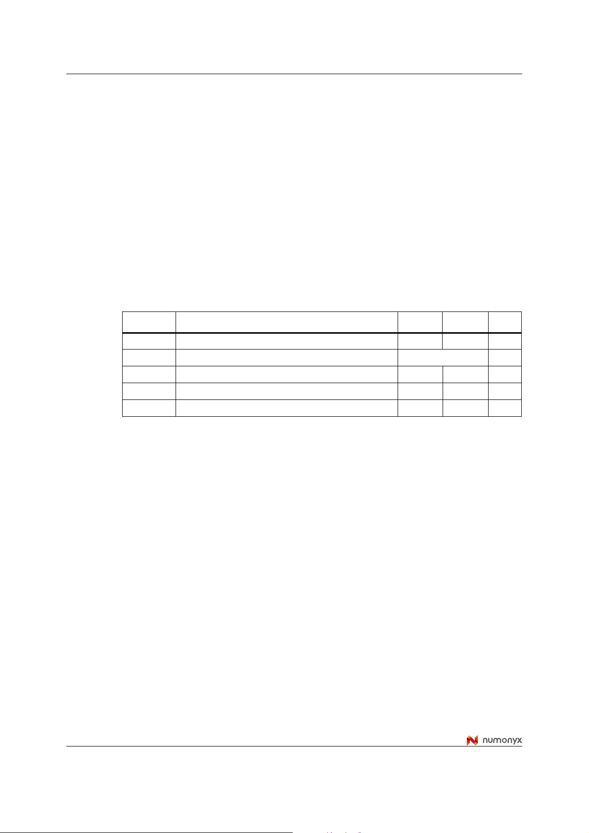
Table 1. Signal names
Signal name Function Direction
C Serial Clock Input
D Serial Data input Input
Q Serial Data output Output
S Chip Select Input
Write Protect Input
W
Reset Input
Reset
V
CC
V
SS
Supply voltage
Ground
7/47

Signal descriptions M45PE10
2 Signal descriptions
2.1 Serial Data output (Q)
This output signal is used to transf er data serially out of the de vice . Data is shifted out on the
falling edge of Serial Clock (C).
2.2 Serial Data input (D)
This input signal is used to transfer data serially into the device. It receives instructions,
addresses, and the data to be programmed. Values are latched on the rising edge of Serial
Clock (C).
2.3 Serial Clock (C)
This input signal provides the timing of the serial interface. Instructions, addresses, or data
present at serial data input (D) are latched on the rising edge of Serial Cloc k (C). Data on
serial data output (Q) changes after the falling edge of Serial Clock (C).
2.4 Chip Select (S)
When this input signal is High, the device is deselect ed and se rial data output (Q) is at high
impedance. Unless an internal read, program, er ase or write cycle is in prog ress , the device
will be in the standby power mode (this is not the deep power-down mode). Driving Chip
Select (S
After power-up, a falling edge on Chip Select (S
instruction.
) Low selects the device, placing it in the active pow er mode.
2.5 Reset (Reset)
The Reset (Reset) input provides a hardw are reset f or the memory. In this mod e, the outputs
are high impedance.
When Reset (Reset
Reset (Reset
operation is currently in prog ress. Driving Reset (Reset
progress has no effect on that internal operation (a write cycle, program cycle, or erase
cycle).
) is driven High, the memory is in the normal operating mode. When
) is driven Low , the memory will enter the reset mode, pro vided that no internal
2.6 Write Protect (W)
This input signal puts the device in the hardware protected mode, when write protect (W) is
connected to V
them from write, program and erase operations. When write protect (W
V
, the first 256 pages of memor y be h ave like the other pages of memory.
CC
, causing the first 256 pages of memory to become read- only by pr otecting
SS
) is required prior to the start of any
) Low while an internal operation is in
) is connected to
8/47

M45PE10 Signal descriptions
2.7 VCC supply voltage
VCC is the supply voltage.
2.8 VSS ground
VSS is the reference for the VCC supply voltage.
9/47

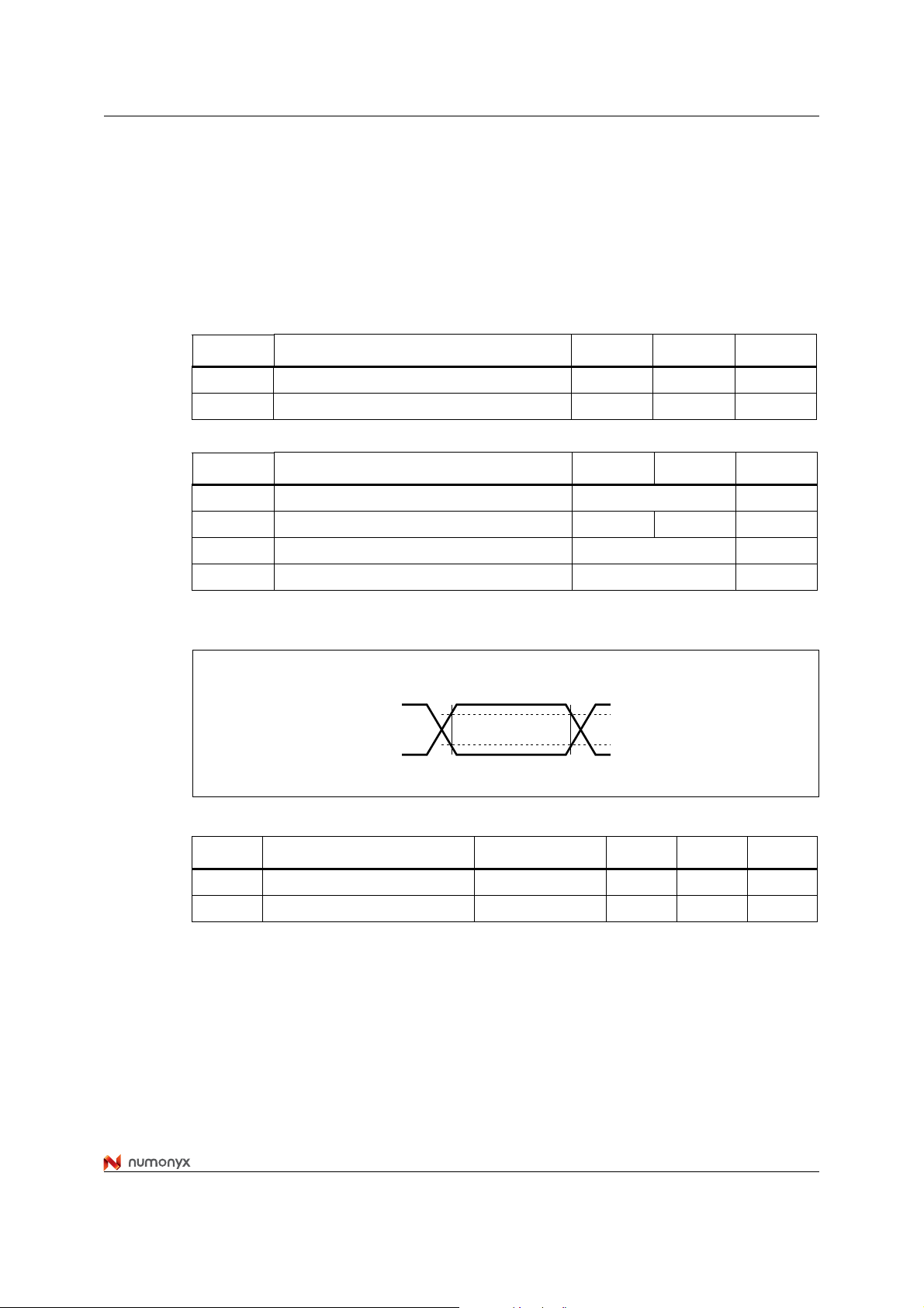
SPI modes M45PE10
3 SPI modes
These devices can be drive n by a microcontroller with its SPI peripheral running in either of
the two following modes:
● CPOL=0, CPHA=0
● CPOL=1, CPHA=1
For these two modes, input data is latched in on the rising edge of Serial Clock (C), and
output data is available from the falling edge of Serial Clock (C).
The difference between the two modes, as shown in Figure 4, is the clock polarity when the
bus master is in standby mode and not transferring data:
● C remains at 0 for (CPOL=0, CPHA=0)
● C remains at 1 for (CPOL=1, CPHA=1)
Figure 3. Bus master and memory devices on the SPI bus
V
SS
V
CC
R
SPI interface with
(CPOL, CPHA) =
(0, 0) or (1, 1)
SPI bus master
CS3 CS2 CS1
1. The Write Protect (W) signal should be driven, High or Low as appropriate.
SDO
SDI
SCK
device
W
V
CC
Reset
CQD
V
SS
SPI memory
S
CQD
RR R
SPI memory
S
device
V
CC
W
Reset
V
CQD
SS
S
V
SPI memory
device
W
CC
Reset
AI12836c
V
SS
Figure 3 shows an examp le of three de vices connected to an MCU , on an SPI bus . Only one
device is selected at a time, so only one device drives the serial data output (Q) line at a
time, the other devices are high impedance.
The pull-up resistor R (represented in Figure 3) ensures that no device is selected if the bus
master leaves the S
line in the high impedance state.
In applications where the bus master might enter a state where all inputs/outputs SPI lines
are in high impedance at the same time (for example, if the bus master is reset during the
transmission of an instruction), the Clock line (C) must be connected to an external pulldown resistor so that, if all inputs/outputs become high impedance, the C line is pulled Low
(while the S
time, and so, that the t
line is pulled High). This ensures that S and C do not become High at the same
requirement is met.
SHCH
10/47

M45PE10 SPI modes
The typical value of R is 100 kΩ, assuming that the time constant R*Cp (Cp = parasitic
capacitance of the bus line) is short enough, as the S
state (S
= High and C = Low) while the SPI bus is in high impedance.
and C lines must reach the correct
Example: C
= 50 pF, that is R*Cp = 5 µs <=> the application must ensure that the bus
p
master never leaves the SPI bus in the high impedance state for a time period shorter than
5µs.
Figure 4. SPI modes supported
CPHA
CPOL
C
0
0
1
1
C
D
Q
MSB
MSB
AI01438B
11/47

Operating features M45PE10
4 Operating features
4.1 Sharing the overhead of modifying data
To write or program one (or more) data bytes, two instructions are required: Write Enable
(WREN), which is one byte, and a page write (PW) or page program (PP) sequence, which
consists of four byte s plus data. This is followed by the internal cycle (of duration t
To share this overhead, the page write (PW) or page program (PP) instruction allows up to
256 bytes to be programmed (changing bits from 1 to 0) or written (changing bits to 0 or 1)
at a time, provided that they lie in consecutive addresses on the same page of memory.
4.2 An easy way to modify data
The page write (PW) instruction provides a convenient way of modifying data (up to 256
contiguous bytes at a time), and simply requires the start address, and the new data in the
instruction sequence.
PW
or tPP).
The page write (PW) instruction is entered by driving Chip Select (S
transmitting the instruction byte, three address bytes (A23-A0) and at least one data byte,
and then driving Chip Select (S
bytes are written to the data buffer, starting at the address given in the third address byte
(A7-A0). When Chip Select (S
unchanged, bytes of the data buffer are automatically loaded with the values of the
corresponding bytes of the addressed memory page. The addressed memory page then
automatically put into an erase cycle. Finally, the addressed memory page is programmed
with the contents of the data buffer.
All of this buffer management is handled internally, and is transparent to the user. The user
is given the facility of being able to alter the contents of the memory on a byte-by-b yte basis .
For optimized timings, it is recommended to use the page write (PW) instruction to write all
consecutive targeted bytes in a single sequence versus using several page write (PW)
sequences with each containing only a few bytes (see Section 6.7: Page write (PW),
Table 14: AC characteristics (50 MHz operation), and Table 15: AC characteristics (75 MHz
operation, T9HX (0.11 µm) process)).
) High. While Chip Select (S) is being held Low, the data
) is driven High, the write cycle starts. The remaining,
) Low, and then
12/47

M45PE10 Operating features
4.3 A fast way to modify data
The Page Program (PP) instruction provides a fast way of modifying data (up to 256
contiguous bytes at a time), pro vided that it only inv olves resetting bits to 0 that had
previously been set to ‘1’.
This might be:
● when the designer is programming the device for the first time
● when the designer knows that the page has already been erased by an earlier page
erase (PE) or sector erase (SE) instruction. This is useful, for example, when storing a
fast stream of data, having first performed the erase cycle when time was available
● when the designer knows that the only changes involve resetting bits to 0 that are still
set to ‘1’. When this method is possible, it has the additional advantage of minimizing
the number of unnecessary erase operations, and the extra stress incurred by each
page.
For optimized timings, it is recommended to use the page program (PP) instruction to
program all consecutive targeted bytes in a single sequence versus using several page
program (PP) sequences with each containing only a few bytes (see Section 6.8: Page
program (PP), Table 14: AC characteristics (50 MHz operation), and Table 15: AC
characteristics (75 MHz operation, T9HX (0.11 µm) process)).
4.4 Polling during a write, program or erase cycle
A further improvement in the write, progra m or erase time can be achie v ed by not w aiting f or
the worst case delay (t
status register so that the application program can monitor its value, polling it to establish
when the previous cycle is complete.
, tPP, tPE, or tSE). The write in progress (WIP) bit is provided in the
PW
4.5 Reset
An internal power on reset circuit helps protect against inadvertent data writes. Addition
protection is provided by driving Reset (Reset
driving it High when V
has reached the correct voltage level, VCC(min).
CC
) Low during the power-on process, and only
4.6 Active power, standby power and deep power-down modes
When Chip Select (S) is Low, the device is selected, and in the active power mode.
When Chip Select (S
mode until all internal cycles have completed (program, er a se, write). The device then goe s
in to the standby power mode. The device consumption drops to I
The deep power-do wn mo de is en tere d when th e specific in struction (the de ep power-down
(DP) instruction) is executed. The device consumption drops further to I
remains in this mode until another specific instruction (the release from deep power-down
and read electronic signature (RES) instruction) is executed.
) is High, the device is dese lected, b ut could rema in in the activ e pow er
.
CC1
. The device
CC2
All other instructions are ignored while the de vice is in the deep pow er-down mo de. This can
be used as an extra softw are protection mech anism, when the device is not in active use, to
protect the device from inadvertent write, program or erase instructions.
13/47

Operating features M45PE10
4.7 Status register
The status register contains two status bits that can be read by the read status register
(RDSR) instruction. See Section 6.4: Read status register (RDSR) for a detailed description
of the status register bits.
4.8 Protection modes
The environments where non-volatile memory devices are used can be very noisy. No SPI
device can operate correctly in the presence of excessive noise. To help comba t this, the
M45PE10 features the following data protection mechanisms:
● Power on reset and an internal timer (t
changes while the power supply is outside the operating specification.
● Program, erase and write instructions are checked that they consist of a number of
clock pulses that is a multiple of eight, before they are accepted for execution.
● All instructions that modify data must be preceded by a write enable (WREN)
instruction to set the write enable latch (WEL) bit. This bit is returned to its reset state
by the following events:
–Power-up
– Reset (Reset
) driven Low
– Write disable (WRDI) instruction completion
– Page write (PW) instruction completion
– Page program (PP) instruction completion
– Page erase (PE) instruction completion
– Sector erase (SE) instruction completion
● The hardwar e protected mod e is entered when write protect (W ) is driven Lo w, causing
the first 256 pages of memory to become read-only. When write protect (W
High, the first 256 pages of memory behave like the other pages of memory
● The Reset (Reset) signal can be driven Low to protect the contents of the memory
during any critical time, not just during power-up and power-down
● In addition to the low power consumption fe ature, the deep power-down mode offers
extra software protection from inadvertent write, program and erase instructions while
the device is not in active use.
) can provide protection against inadvertent
PUW
) is driven
14/47

M45PE10 Memory organization
5 Memory organization
The memory is organized as:
● 512 pages (256 bytes each)
● 131,072 bytes (8 bits each)
● 2 sectors (512 Kbits, 65536 bytes each)
Each page can be individually:
● programmed (bits are programmed from 1 to 0)
● erased (bits are erased from 0 to 1)
● written (bits are changed to either 0 or 1)
The device is page or sector erasa ble (bits are erased from 0 to 1).
Table 2. Memory organization
Sector Address range
1 10000h 1FFFFh
0 00000h 0FFFFh
15/47
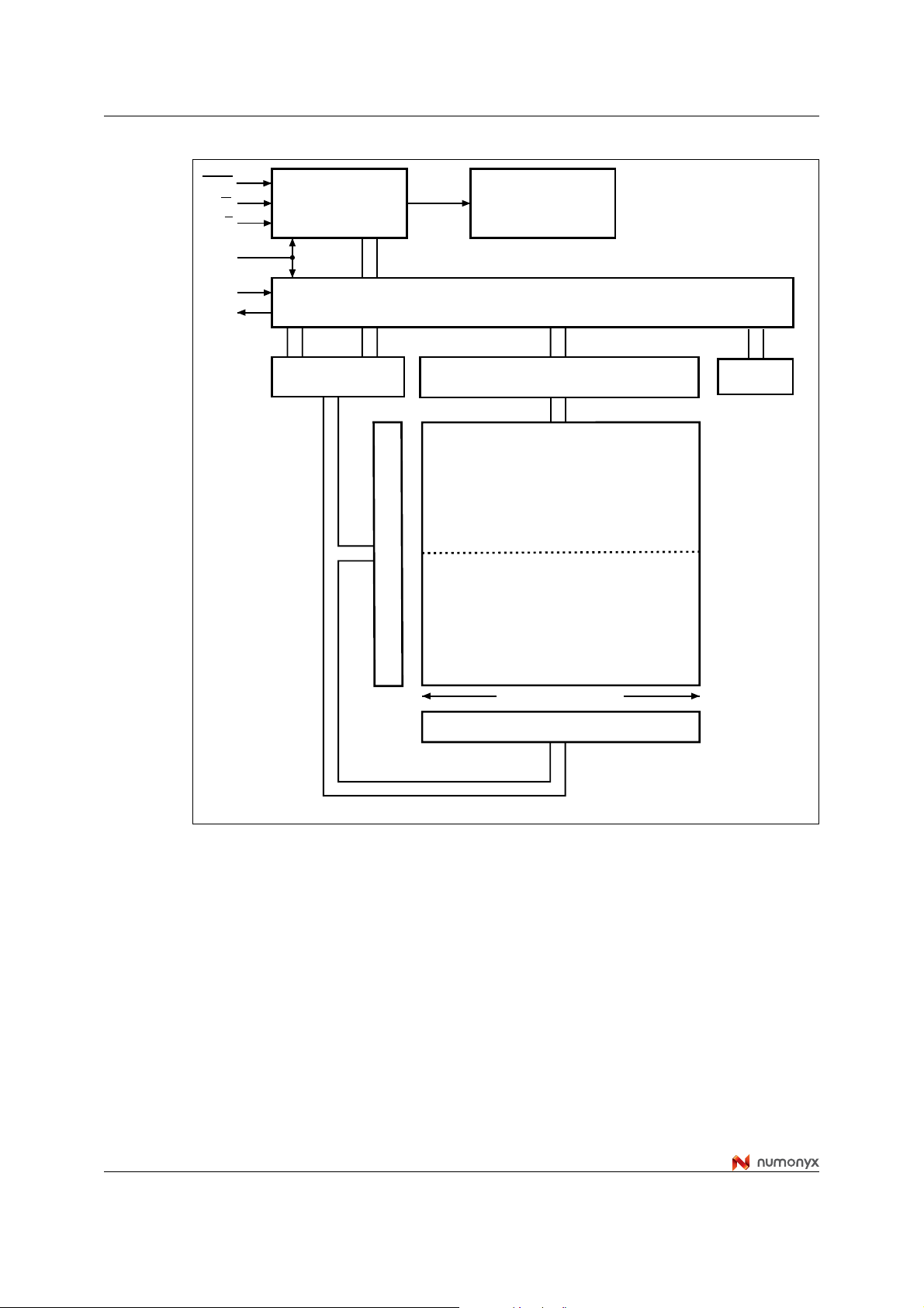
Memory organization M45PE10
Figure 5. Block diagram
Reset
W
S
C
D
Q
Control logic
Address register
and counter
10000h
Ydecoder
High voltage
generator
I/O shift register
256-byte
data buffer
Status
register
1FFFFh
First 256 pages can
be made read-only
00000h
000FFh
256 bytes (page size)
X decoder
AI07405
16/47
M45PE10 Instructions
6 Instructions
All instructions, addresses and data are shifted in and ou t of the device, most significant bit
first.
Serial data input (D) is sampled on the first rising edge of Serial Clock (C) after Chip Select
(S
) is driven Low. Then, the one-byte instruction code must be shif te d in to t he device, most
significant bit first, on serial data input (D), each bit being latched on the rising edges of
Serial Clock (C).
The instruction set is listed in Table 3.
Every instruction sequence starts with a one-byte instruction code. Depending on the
instruction, this might be followed by address bytes, or by data bytes, or by both or none.
In the case of a read data bytes (READ), read data bytes at higher speed (FAST_READ) or
read status register (RDSR) instruction, the shifted-in instruction sequence is followed by a
data-out sequence. Chip Select (S
sequence is being shifted out.
In the case of a page write (PW), page program (PP), page erase (PE), sector erase (SE),
write enable (WREN), write disable (WRDI), deep power-down (DP) or release from deep
power-down (RDP) instruction, Chip Select (S
boundary, otherwise the instruction is rejected, and is not executed. T hat is, Chip Select (S
must driven High when the number of clock pulses after Chip Select (S
an exact multiple of eight.
) can be driven High after any bit of the data-out
) must be driven High exactly at a byte
) being driven Low is
)
All attempts to access the memory array during a write cycle, program cycle or erase cycle
are ignored, and the internal write cycle, program cycle or erase cycle continues unaffected.
Table 3. Instruction set
Instruction Description
WREN Write enable 0000 0110 06h 0 0 0
WRDI Write disable 0000 0100 04h 0 0 0
RDID Read identification 1001 1111 9Fh 0 0 1 to 3
RDSR Read status register 0000 0101 05h 0 0 1 to ∞
READ Read data bytes 0000 0011 03h 3 0 1 to ∞
FAST_READ
PW Page write 0000 1010 0Ah 3 0 1 to 256
PP Page program 0000 0010 02h 3 0 1 to 256
PE Page erase 1101 1011 DBh 3 0 0
SE Sector erase 1101 1000 D8h 3 0 0
DP Deep power-down 1011 1001 B9h 0 0 0
RDP
Read data bytes at higher
speed
Release from deep
power-down
One-byte instruction
code
0000 1011 0Bh 3 1 1 to ∞
1010 1011 ABh 0 0 0
Address
bytes
Dummy
bytes
Data
bytes
17/47

Instructions M45PE10
6.1 Write enable (WREN)
The write enable (WREN) instruction (Figure 6) sets the write enable latch (WEL) bit.
The write enable latch (WEL) bit must be set prior to every page write (PW), page program
(PP), page erase (PE), and sector erase (SE) instruction.
The write enable (WREN) instruction is entered by driving Chip Select (S
instruction code, and then driving Chip Select (S
Figure 6. Write enable (WREN) instruction sequence
S
C
D
Q
6.2 Write disable (WRDI)
The write disable (WRDI) instruction (Figure 7 ) resets the write enable latch (WEL) bit.
The write disable (WRDI) instruction is entered by driving Chip Select (S
instruction code, and then driving Chip Select (S
The write enable latch (WEL) bit is reset under the following conditions:
● Power-up
● Write disable (WRDI) instruction completion
● Page write (PW) instruction completion
● P age program (PP) instruction completion
● Page erase (PE) instruction completion
● Sector erase (SE) instruction completion
0
21 34567
Instruction
High Impedance
) Low, sending the
) High.
AI02281E
) Low, sending the
) High.
Figure 7. Write disable (WRDI) instr uction sequence
S
0
21 34567
C
D
High Impedance
Q
18/47
Instruction
AI03750D

M45PE10 Instructions
6.3 Read identification (RDID)
The read identification (RDID) instruction allows to read the device identification data:
● Manufacturer identification (1 byte)
● Device identification (2 bytes)
● A unique ID code (UID) (17 bytes, of which 16 available upon customer request)
The manufactur er id entifica tion is assigne d b y JEDEC, and has the value 20h for Numon yx.
The device identif ication is assigned by the device manufacturer, and indicates the memory
type in the first byte (40h), and the memory capacity of the device in the second byte (11h).
The UID contains the length of the following data in the first byte (set to 10h), and 16 bytes
of the optional customized factory data (CFD) content . The CFD bytes are read-only and
can be programmed with cust omers data upon their demand. If the customers do not make
requests, the devices are shipped with all the CFD bytes programmed to zero (00h).
Any read identification (RDID) instruction while an erase or program cycle is in progress, is
not decoded, and has no effect on the cycle that is in progress.
(a)
.
The device is first selected by driving Chip Select (S
) Low. Then, the 8-bit instruction code
for the instruction is shifted in. After this, the 24-bit device identification, stored in the
memory, the 8-bit CFD length followed by 16 bytes of CFD content will be shifted out on
serial data output (Q). Each bit is shifted out during the falling edge of Serial Clock (C).
The instruction sequence is shown in Figure 8.
The Read Identification (RDID) instruction is terminated by driving Chip Select (S
any time during data output.
When Chip Select (S
) is driven High, the device is put in the st andby power mode. Once in
the standby pow er mode , the device waits to be selected, so that it can receive , decode a nd
execute instructions.
Table 4. Read identification (RDID) data-out sequence
Manufacturer
Identification
1. The unique ID code is available only in the T9HX process (see Important note on page 6).
Device Identification UID
Memory type Memory capacity CFD length CFD content
20h 40h 11h 10h 16 bytes
) High at
(1)
a. The 17 bytes of unique ID code are available only in the T9HX process (see Important note on
page 6).
19/47
Instructions M45PE10
Figure 8. Read identification (RDID) instruction sequence and data-out sequence
S
0
213456789101112131415
C
Instruction
D
16 17 18 28 29 30 31
Q
1. The unique ID code is available only in the T9HX process (see Important note on page 6).
High Impedance
Manufacturer identification
MSB
Device identification
15
14 13 3 2 1 0
MSB
6.4 Read status register (RDSR)
The read status register (RDSR) instruction allows t he status re gister to be read. The status
register may be read at any time, even while a program, erase or write cycle is in progress.
When one of these cycles is in progress, it is recommended to check the write in progress
(WIP) bit before sending a ne w in struction to the de vice . It is al so possibl e to read the stat us
register continuously, as shown in Figure 9.
The status bits of the status register are as follows:
6.4.1 WIP bit
The write in progress (WIP) bit indicates whether the memory is busy with a write, program
or erase cycle. When set to ‘1’, such a cycle is in progress , when reset to ‘ 0’ no such cycle is
in progress.
6.4.2 WEL bit
UID
MSB
AI06809c
The write enable latch (WEL) bit indicates the status of the internal write enable latch. When
set to ‘1’ the internal write enable latch is set, when set to ‘0’ the internal write enable latch is
reset and no write, program or erase instruction is accepted.
Table 5. Status register format
b7 b0
0 0 0 0 0 0 WEL
1. WEL and WIP are volatile read-only bits (WEL is set and reset by specific instructions; WIP is
automatically set and reset by the internal logic of the device).
20/47
(1)
WIP
(1)
M45PE10 Instructions
Figure 9. Read status register (RDSR) instruction sequence and data -out sequence
S
21 3456789101112131415
0
C
Instruction
D
Q
High Impedance
6.5 Read data bytes (READ)
The device is first selected by driving Chip Select (S) Low. The instruction code for the read
data bytes (READ) instruction is f ollowed by a 3-byte address (A23-A0), each bit being
latched-in during the rising edge of Serial Clock (C). Then the memory contents, at that
address, is shifted out on serial data output (Q), each bit being shifted out, at a maximum
frequency f
The instruction sequence is shown in Figure 10.
The first byte addressed can be at any location. The address is automatically incremented
to the next higher address after each byte of data is shifted out. The whole memory can,
therefore, be read with a single read data bytes (READ) instruction. When the highest
address is reached, the address counter rolls over to 000000h, allowing the read sequence
to be continued indefinitely.
The read data bytes (READ) instruction is terminated by driving Chip Select (S
select (S
instruction, while an erase, program or write cycle is in progress, is rejected without having
any effects on the cycle that is in progress.
, during the falling edge of Serial Clock (C).
R
) can be driven High at any time during data output. Any read data bytes (READ)
Status Register Out
7 6543210
MSB
Status Register Out
7 6543210
MSB
7
AI02031E
) High. Chip
21/47
Instructions M45PE10
Figure 10. R ead data bytes (READ) instruction sequence and data-out sequence
S
21 345678910 2829303132333435
0
C
Instruction 24-bit address
D
High Impedance
Q
1. Address bits A23 to A17 are don’t care.
23
2221 3210
MSB
36 37 38
Data out 1
76543 1 7
MSB
39
2
0
Data out 2
AI03748D
22/47

M45PE10 Instructions
6.6 Read data bytes at higher speed (FAST_READ)
The device is first selected by driving Chip Select (S) Low. The instruction code for the read
data bytes at higher speed (FAST_READ) instruction is followed by a 3-byte address (A23A0) and a dummy byte, each bit being latched-in during the rising edge of Serial Clock (C).
Then the memory contents, at that address , is shifted out on serial data ou tput (Q ), ea ch bit
being shifted out, at a maximum frequency f
The instruction sequence is shown in Figure 11.
The first byte addressed can be at any location. The address is automatically incremented
to the next higher address after each byte of data is shifted out. The whole memory can,
therefore, be read with a single read data bytes at higher speed (FAST_READ) instruction.
When the highest address is reached, the address counter rolls over to 000000h, allowing
the read sequence to be continued indefinite ly.
The read data bytes at higher speed (FAST_READ) instruction is terminated by driving Chip
Select (S
) High. Chip select (S) can be driven High at an y time during data output . An y read
data bytes at higher speed (F AST_READ) instruction, while an erase, program or write cycle
is in progress, is rejected without having any effects on the cycle that is in progress.
Figure 11. Read data bytes at higher speed (FAST_READ) instruction sequence
and data-out sequence
, during the falling edge of Serial Clock (C).
C
S
21 345678910 28293031
0
C
Instruction 24-bit address
D
High Impedance
Q
S
32 33 34 36 37 38 39 40 41 42 43 44 45 46
C
D
Q
1. Address bits A23 to A17 are don’t care.
765432 0
35
Dummy byte
1
23
2221 3210
DATA OUT 1
765432 0
MSB
47
DATA OUT 2
7 6543210
1
MSB MSB
7
AI04006
23/47

Instructions M45PE10
6.7 Page write (PW)
The page write (PW) instruction allows bytes to be written in the memory. Before it can be
accepted, a write enable (WREN) instruction must pre viously ha v e been e xecuted. After the
write enable (WREN) instruction has been decoded, the device sets the write enable latch
(WEL).
The page write (PW) instruction is entered by driving Chip Select (S
instruction code, three address b ytes and a t least one data b yte on serial data input ( D). The
rest of the page remains unchanged if no power failure occurs during this write cycle.
The page write (PW) instruction performs a page erase cycle even if only one byte is
updated.
If the 8 least significant address bits (A7-A0) are not all zero, all transmitted data exceeding
the addressed page boundary wrap round, and are written from the start address of the
same page (the one whose 8 least significan t address bits (A7-A0) are a ll zero) . Chip Select
(S
) must be driven Low for the entire duration of the sequence.
The instruction sequence is shown in Figure 12.
If more than 256 by tes ar e se nt t o the device, previously latched data are discard ed and the
last 256 data bytes are guarantee d to be written correctly withi n the same pa ge . If less than
256 data bytes are sent to device, they are correctly written at the requested addresses
without having any effects on the other bytes of the same page.
For optimized timings, it is recommended to use the page write (PW) instruction to write all
consecutive targeted bytes in a single sequence versus using several page write (PW)
sequences with each containing only a few bytes (see Table AC characteristics (50 MHz
operation) and Table 15: AC characteristics (75 MHz operation, T9HX (0.11 µm) process)).
Chip Select (S
latched in, otherwise the page write (PW) instruction is not executed.
As soon as Chip Select (S
t
) is initiated. While the page write cycle is in progress , t he stat us regist er may be read to
PW
check the va lue of t he write in prog ress (WIP) bit. The write in progr ess (WIP) bit is 1 du ring
the self-timed page write cycle, and is 0 when it is completed. At some unspecified time
before the cycle is complete, the write enable latch (WEL) bit is reset.
) must be driven High after the eighth bit of the last data byte has been
) is driven High, the self-timed page write cycle (whose duration is
) Low, followed by the
A page write (PW) instruction applied to a page that is hardware protected is not executed.
Any page write (PW) instruction, while an erase, program or write cycle is in progress, is
rejected without having any effects on the cycle that is in progress.
24/47
M45PE10 Instructions
Figure 12. Page write (PW) instruction sequence
S
21 345678910 2829303132333435
0
C
Instruction 24-bit address
D
S
4241 43 44 45 46 47 48 49 50 52 53 54 5540
C
Data byte 2
D
765432 0
MSB MSB MSB
1
1. Address bits A23 to A17 are don’t care.
2. 1 ≤ n ≤ 256.
23
2221 3210
MSB
51
Data byte 3 Data byte n
765432 0
1
765432 0
MSB
765432 0
36 37 38
Data byte 1
39
1
1
AI04045
25/47

Instructions M45PE10
6.8 Page program (PP)
The page program (PP) instruction allo ws bytes to b e programmed in t he memory (changing
bits from 1 to 0, only). Before it can be accepted, a Write Enable (WREN) instruction must
previously have been executed. After the write enable (WREN) in struction has been
decoded, the device sets the write enable latch (WEL).
The page program (PP) instruction is entered b y driving Chip Select (S
instruction code, three address bytes and at least one data byte on serial data input (D). If
the 8 least significant address bits (A7-A0) are not all zero, all transmitted data exceeding
the addressed page boundary wrap round, and are programmed from the start address of
the same page (the one whose 8 least significant address bits (A7-A0) are all zero). Chip
Select (S
The instruction sequence is shown in Figure 13.
If more than 256 by tes ar e se nt t o the device, previously latched data are discard ed and the
last 256 data bytes are guaranteed t o be progr ammed correctly within the same page . If less
than 256 data bytes are sent to device, they are correctly programmed at the requested
addresses without having any effects on the other bytes of the same page.
For optimized timings, it is recommended to use the page program (PP) instruction to
program all consecutive targeted bytes in a single sequence versus using several page
program (PP) sequences with each containing only a few bytes (see Table 14: AC
characteristics (50 MHz operation) and Table 15: AC characteristics (75 MHz operation,
T9HX (0.11 µm) process)).
Chip Select (S
latched in, otherwise the page progr am (PP) instruction is not ex ecuted.
As soon as Chip Select (S
duration is t
may be read to check th e value of the write in progress (WIP) bit. The write in progress
(WIP) bit is 1 during the self-timed page program cycle, and is 0 when it is completed. At
some unspecified time before t he cycle is complete , the write enab le latch (WEL) bit is reset.
) must be driven Low for the entire duration of the sequence.
) must be driven High after the eighth bit of the last data byte has been
) is driven High, the self-timed page program cycle (whose
) is initiated. While the page program cycle is in progress, the status register
PP
) Low, f ollowed b y the
A page program (PP) instruction applied to a page that is hardware protected is not
executed.
Any page program (PP) instruction, while an erase, program or write cycle is in progress, is
rejected without having any effects on the cycle that is in progress.
26/47

M45PE10 Instructions
Figure 13. Page program (PP) instruction sequence
S
21 345678910 2829303132333435
0
C
36 37 38
39
Instruction 24-bit address
D
S
4241 43 44 45 46 47 48 49 50 52 53 54 5540
C
Data byte 2
D
765432 0
MSB MSB MSB
1
1. Address bits A23 to A17 are don’t care.
2. 1 ≤ n ≤ 256.
23
2221 3210
MSB
51
Data byte 3 Data byte n
765432 0
1
765432 0
MSB
765432 0
Data byte 1
1
1
AI04044
27/47
Instructions M45PE10
6.9 Page erase (PE)
The page erase (PE) instruction sets to ‘1’ (FFh) all bits inside the chosen page. Before it
can be accepted, a write enable (WREN) instruction must previously have been executed.
After the write enable (WREN) instruction has been decoded, the device sets the write
enable latch (WEL).
The page erase (PE) instruction is entered by driving Chip Select (S
) Low, followed by the
instruction code, and three address bytes on serial data input (D). Any address inside the
page is a valid address f or the page erase (PE) instruction. Chip Select (S
) must be driven
Low for the entire duration of the sequence.
The instruction sequence is shown in Figure 14.
Chip Select (S
) must be driven High after the eighth bit of the last address byte has been
latched in, otherwise the page erase (PE) instruction is not executed. As soon as Chip
Select (S
) is driven High, the self-timed page erase cycle (whose d uratio n is tPE) is initiated.
While the page erase cycle is in progress, the status register ma y be read to check the v alue
of the write in progress (WIP) bit. The write in progress (WIP) bit is 1 during the self-timed
page erase cycle, and is 0 when it is completed. At some unspecified time before the cycle
is complete, the write enable latch (WEL) bit is reset.
A page erase (PE) instruction applied to a page that is hardwa re protected is not executed.
Any page erase (PE) instruction, while an erase, program or write cycle is in progress, is
rejected without having any effects on the cycle that is in progress.
Figure 14. Page erase (PE) instruction sequence
S
21 3456789 293031
0
C
Instruction
D
1. Address bits A23 to A17 are don’t care.
28/47
24-bit address
23 22 2 0
MSB
1
AI04046

M45PE10 Instructions
6.10 Sector erase (SE)
The sector erase (SE) instruction sets to ‘1’ (FFh) all bits inside the chosen sector. Before it
can be accepted, a write enable (WREN) instruction must previously have been executed.
After the write enable (WREN) instruction has been decoded, the device sets the write
enable latch (WEL).
The sector erase (SE) instruction is entered by driving Chip Select (S
) Low, followed by the
instruction code, and three address bytes on serial data input (D). Any address inside the
sector (see Table 2) is a valid address for the sector erase (SE) instruction. Chip Select (S
must be driven Low for the entire duration of the sequence.
The instruction sequence is shown in Figure 15.
Chip Select (S
) must be driven High after the eighth bit of the last address byte has been
latched in, otherwise the sector erase (SE) instruction is not executed. As soon as Chip
Select (S
) is driven High, the self-timed sector erase cycle (whose duration is tSE) is
initiated. While the sector erase cycle is in progress, the status register may be read to
check the va lue of t he write in prog ress (WIP) bit. The write in progr ess (WIP) bit is 1 du ring
the self-timed sector erase cycle, and is 0 when it is completed. At some unspecified time
before the cycle is complete, the write enable latch (WEL) bit is reset.
A sector erase (SE) instruction applied to a sector that contains a page that is Hardware
Protected is not executed.
Any sector erase (SE) instruction, while an erase, program or write cycle is in progress, is
rejected without having any effects on the cycle that is in progress.
Figure 15. Sector erase (SE) instruction sequence
S
0
C
21 3456789 293031
)
Instruction
D
1. Address bits A23 to A17 are don’t care.
24-bit address
23 22 2 0
MSB
29/47
1
AI03751D

Instructions M45PE10
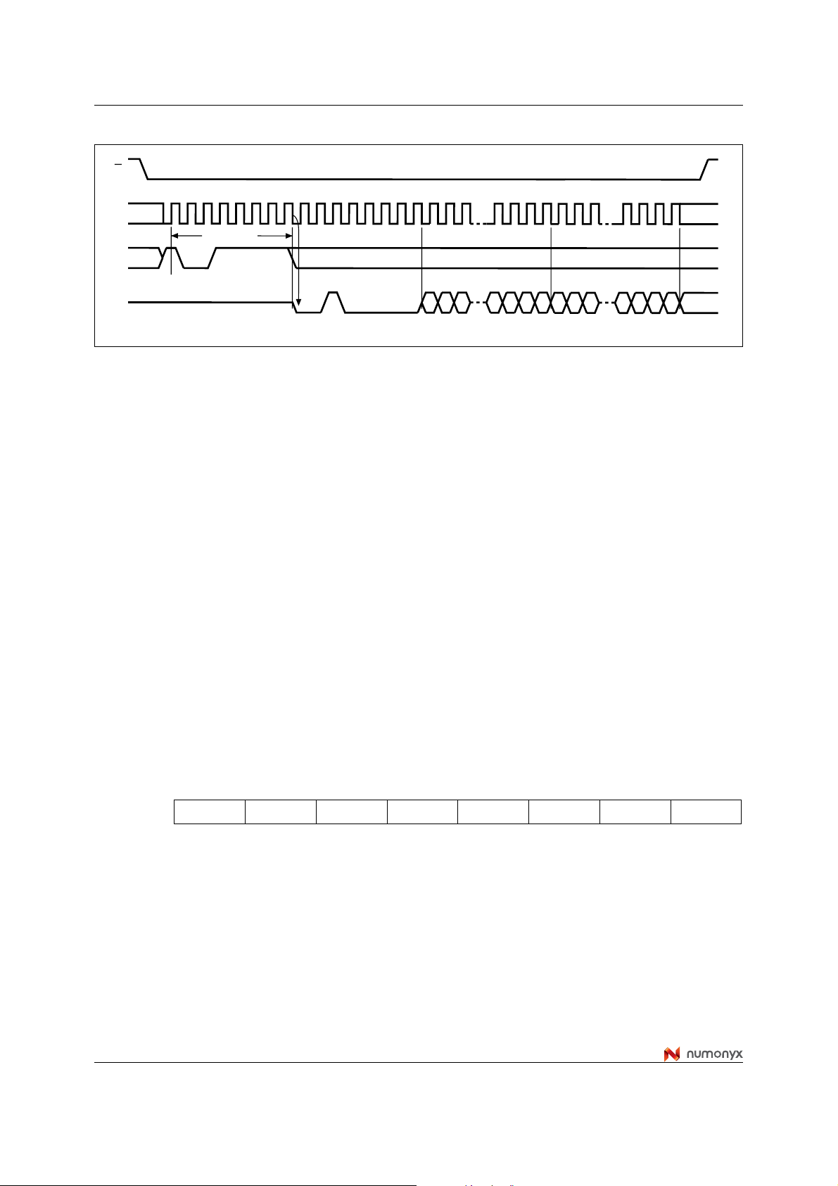
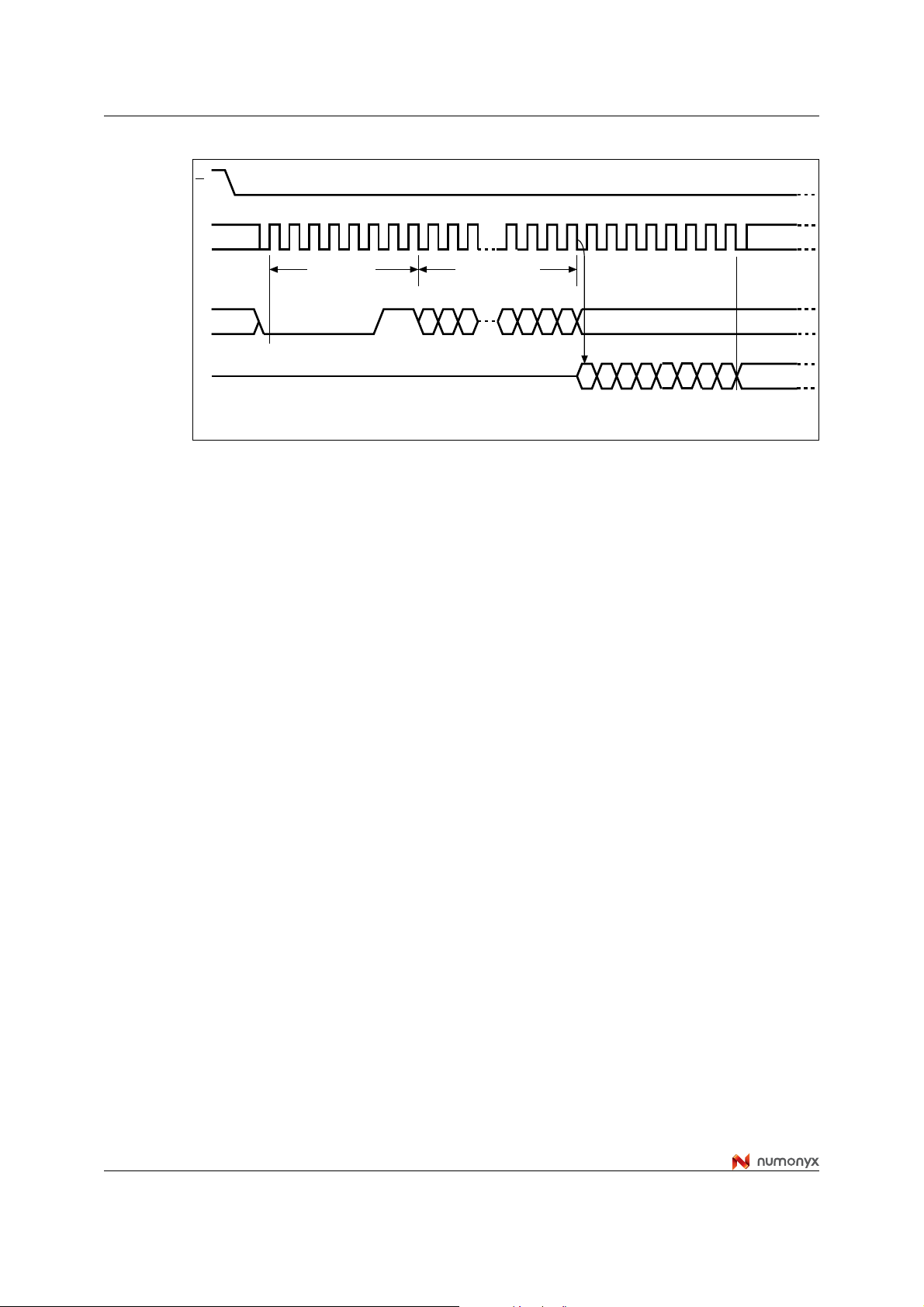
6.11 Deep power-down (DP)
Executing the deep power-down (DP) instruction is the only way to put the device in the
lowest consumption mode (the deep power-down mode). It can also be used as an extra
software protection mechanism, while th e device is not in active use, since in this mode, th e
device ignores all write, program and erase instructions.
Driving Chip Select (S
) High deselects the device, and puts the device in the standby power
mode (if there is no internal cycle currently in progress). But this mode is not the deep
power-down mode. The dee p pow er-do wn mode can only be ent ered b y e x e cuting the deep
power-down (DP) instruction, to reduce the standby current (from I
CC1
to I
, as specified
CC2
in Table 11).
Once the device has entered the deep power-down mode, all instructions are ignored
except the release from deep power-down (RDP) instruction. This releases the device from
this mode.
The deep power-down mode automatically stops at power-down, and the device always
powers-up in the standby power mode.
The deep power-down (DP) instruction is entered by driving Chip Select (S
by the instruction code on Serial Data input (D). Chip Select (S
) must be driven Low for the
) Low, followed
entire duration of the sequ ence.
The instruction sequence is shown in Figure 16.
Chip Select (S
) must be driven High after the eighth bit of the instruction code has been
latched in, otherwise the deep power-down (DP) instruction is not executed. As soon as
Chip Select (S
to I
and the deep power-down mode is entered.
CC2
) is driven High, it requires a delay of tDP before the supply cu rrent is r educe d
Any deep power-down (DP) instruction, while an erase, program or write cycle is in
progress, is rejected without having any effects on the cycle that is in progress.
Figure 16. Deep power-down (DP) instruction sequence
S
21 345670
C
Instruction
D
30/47
t
DP
Standby mode
Deep power-down mode
AI03753D

M45PE10 Instructions
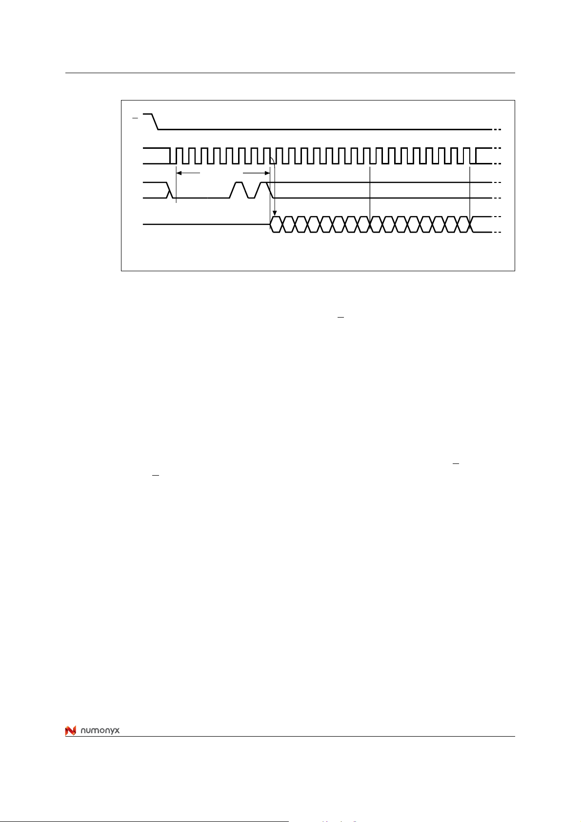
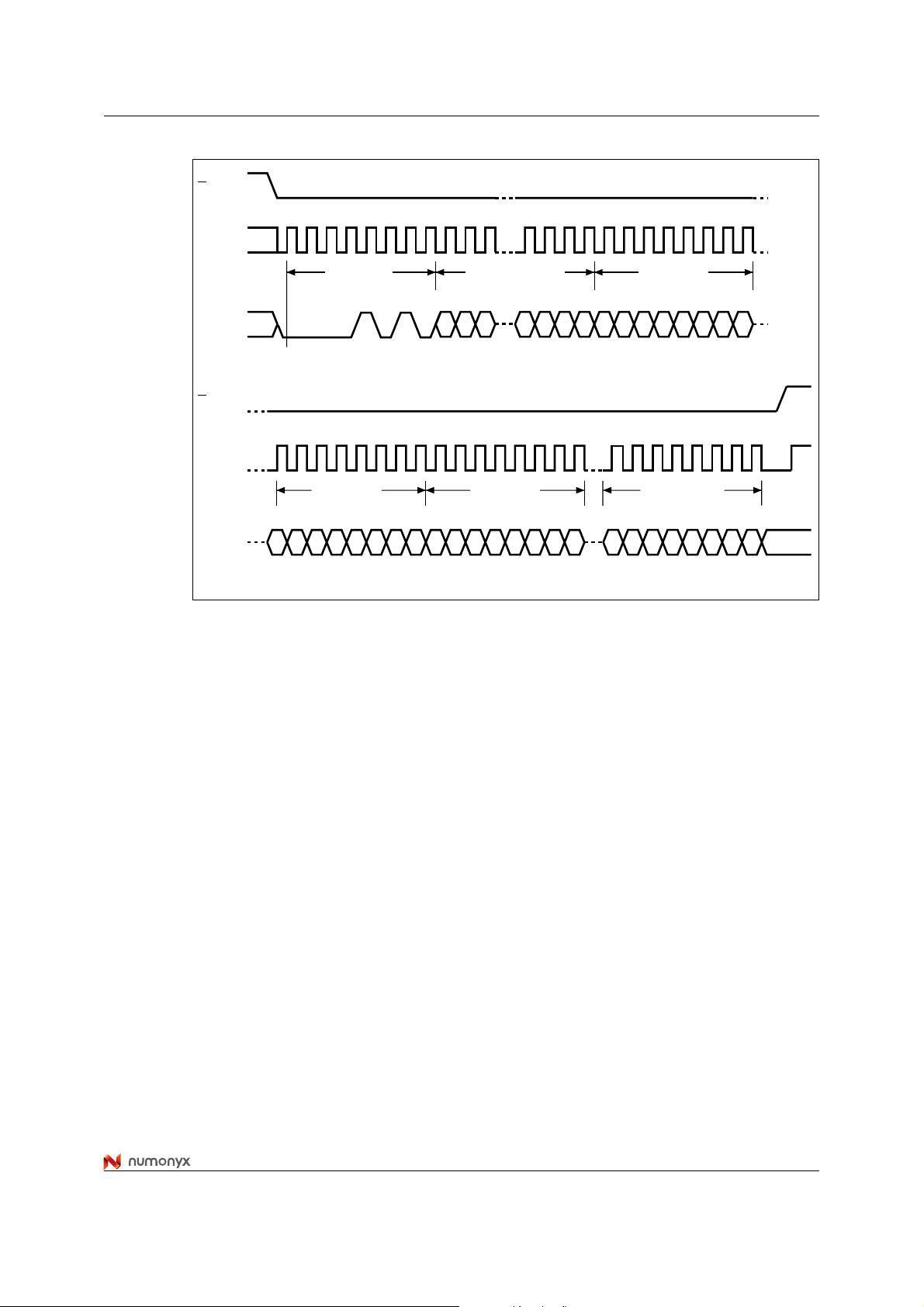
6.12 Release from deep power-down (RDP)
Once the device has entered the deep power-down mode, all instructions are ignored
except the release from deep power-down (RDP) instruction. Executing this instruction
takes the device out of the deep power-down mode.
The release from deep pow er-down (RDP) instruction is entered by driving Chip Select (S
Low, followed by the instruction code on Serial Data input (D). Chip Select (S
) must be
driven Low for the entire duration of the sequence.
The instruction sequence is shown in Figure 17.
The release from deep power-down (RDP) instruction is terminated by driving Chip Select
(S
) High. Sending additional clock cycles on Serial Clock (C), while Chip Select (S) is driven
Low, cause the instruction to be rejected, and not executed.
After Chip Select (S
Standby P ow er mode. Chip Sele ct (S
) has been driven High, fo llow ed b y a delay, t
) must remain High at least until this period is over. The
, the device is put in the
RDP
device waits to be selected, so that it can receive, decode and execute instructions.
Any release from deep power-down (RDP) instruction, while an erase, program or write
cycle is in progress, is rejected without having any effects on the cycle that is in progress.
Figure 17. Release from deep power-down (RDP) instruction sequence
S
t
21 345670
C
Instruction
RDP
)
D
High Impedance
Q
Deep power-down mode
Standby mode
AI06807
31/47

Power-up and power-down M45PE10
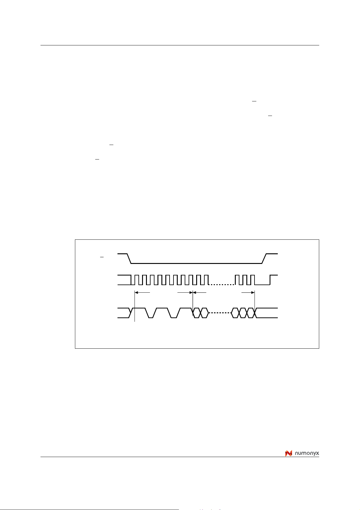
7 Power-up and power-down
At power-up and po w er- down, the device must not be selected (that is Chip Select (S) must
follow the voltage applied on V
● V
●
(min) at power-up, and then for a further delay of t
CC
VSS at power-down
A safe configuration is provided in Section 3: SPI modes.
To avoid data corruption and inadv ertent write operations during pow er up , a pow er on reset
(POR) circuit is included. The logic inside the device is held reset while V
power on reset (POR) threshold value, V
does not respond to any instruction.
Moreover , the de vice ignores all write enable (WREN), page write (PW), page prog ram (PP),
page erase (PE) and sector erase (SE) instructions until a time delay of t
after the moment that V
CC
the device is not guaranteed if, by this time, V
erase instructions should be sent until the later of:
● t
● t
after VCC passed the VWI threshold
PUW
after wrap round VCC passed the VCC(min) level
VSL
These values are specified in Table 6.
) until VCC reaches the correct value:
CC
VSL
is less than the
– all operations are disabled, and the device
WI
CC
has elapsed
PUW
rises above the VWI threshold. However, the correct operat ion of
is still below VCC(min). No write, program or
CC
If the delay, t
selected for read instructions even if the t
As an extra protect ion, t he Reset ( Reset
, has elapsed, after VCC has risen above VCC(min), the device can be
VSL
delay is not yet fully elapsed.
PUW
) signal can be driven Lo w for the whole duration of
the power-up and power-down phases.
At power-up, the device is in the following state:
● The device is in the standby power mode (not the deep power-down mode)
● The write enable latch (WEL) bit is reset
● The write in progress (WIP) bit is reset
Normal precautions must be taken for supply rail decoupling, to stabilize the V
Each device in a system should ha ve t he V
line decoupled by a suitable capacitor close to
CC
supply.
CC
the package pins (generally, this capacitor is of the order of 100 nF).
At power-down, when V
(POR) threshold value, V
drops from the operating voltage, to below the power on reset
CC
, all operations are disabled and the device does not respond to
WI
any instruction (the designer needs to be aware that if a power-down occurs while a write,
program or erase cycle is in progress, some data corruption can result).
32/47
M45PE10 Power-up and power-down
Figure 18. Power-up timing
V
CC
VCC(max)
Program, erase and write commands are rejected by the device
Chip selection not allowed
VCC(min)
Reset state
of the
V
WI
Table 6. Power-up timing and VWI threshold
device
tVSL
tPUW
Symbol Parameter Min. Max. Unit
(1)
t
VSL
t
PUW
V
1. These parameters are characterized only, over the temperature range –40 °C to +85 °C.
WI
VCC(min) to S low 30 µs
(1)
Time delay before the first write, program or erase instruction 1 10 ms
(1)
Write inhibit voltage 1.5 2.5 V
Read access allowed Device fully
accessible
time
AI04009C
33/47
Initial delivery state M45PE10
8 Initial delivery state
The device is deliv ered with the memory array erased: all bits are set to ‘1’ (each byte
contains FFh). All usable status register bits are 0.
9 Maximum ratings
Stressing the device outside th e ratings listed in Table 7 : Abs olu te max imum ratings may
cause permanent damage to the device. These are stress ratings only, and operation of the
device at these, or any other conditions outside those indicated in the operating sections of
this specification, is not implied. Exposure to absolute maximum rating conditions for
extended periods may aff ect device reliability.
Table 7. Absolute maximum ratings
Symbol Parameter Min. Max. Unit
T
STG
T
LEAD
V
IO
V
CC
V
ESD
1. Compliant with JEDEC Std J-STD-020C (for small body, Sn-Pb or Pb assembly), the Numonyx
ECOPACK® 7191395 specification, and the European directive on Restrictions on Hazardous Substances
(RoHS) 2002/95/EU.
2. JEDEC Std JESD22-A114A (C1=100pF, R1=1500 Ω , R2=500 Ω).
Storage temperature –65 150 °C
Lead temperature during soldering See note
(1)
Input and output voltage (with respect to ground) –0.6 VCC + 0.6 V
Supply voltage –0.6 4.0 V
Electrostatic discharge voltage (human body model)
(2)
–2000 2000 V
°C
34/47
M45PE10 DC and AC parameters
10 DC and AC parameters
This section summarizes the operating and measurement conditions, and the DC and AC
characteristics of the device. The parameters in the DC and AC characteristic tables that
follow are derived from tests performed under the measurement conditions summarized in
the relevant tables. Designers should check that the operating conditions in their circuit
match the measurement conditions when relying on the quoted parameters.
Table 8. Operating conditions
Symbol Parameter Min. Max. Unit
V
CC
T
Table 9. AC measurement conditions
Supply voltage 2.7 3.6 V
Ambient operating temperature –40 85 °C
A
Symbol Parameter Min. Max. Unit
C
Load capacitance 30 pF
L
Input rise and fall times 5 ns
Input pulse voltages 0.2VCC to 0.8V
Input and output timing reference voltages 0.3V
1. Output Hi-Z is defined as the point where data out is no longer driven.
to 0.7V
CC
CC
CC
Figure 19. AC measurement I/O waveform
Input levels
0.8V
0.2V
Table 10. Capacitance
CC
CC
(1)
Input and output
timing reference levels
0.7V
CC
0.3V
CC
AI00825B
V
V
Symbol Parameter Test condition Min. Max. Unit
C
OUT
C
IN
1. Sampled only, not 100% tested, at T
Output capacitance (Q) V
Input capacitance (other pins) VIN = 0 V 6 pF
=25 °C and a frequency of 33 MHz.
A
= 0 V 8 pF
OUT
35/47

DC and AC parameters M45PE10
Table 11. DC characteristics
Symbol Parameter
I
Input leakage current ± 2 µA
LI
Output leakage current ± 2 µA
I
LO
Standby current
I
(standby and reset
CC1
modes)
I
I
I
I
V
V
Deep power-do w n
CC2
current
Operating current
CC3
(FAST_READ)
Operating current (PW) S = V
CC4
Operating current (SE) S = V
CC5
V
Input low voltage – 0.5 0.3V
IL
Input high voltage 0.7V
V
IH
Output low voltage IOL = 1.6 mA 0.4 V
OL
Output high voltage IOH = –100 µA VCC–0.2 V
OH
Test condition
(in addition to those in Table 8)
S = VCC, V
= VCC, V
S
= VSS or V
IN
= VSS or V
IN
CC
CC
C = 0.1VCC / 0.9.VCC at 33 MHz,
Q = open
C = 0.1V
/ 0.9.VCC at 75 MHz,
CC
Q = open
CC
CC
Min. Max. Unit
50 µA
10 µA
4
mA
12
15 mA
15 mA
V
CCVCC
CC
+0.4 V
36/47
M45PE10 DC and AC parameters
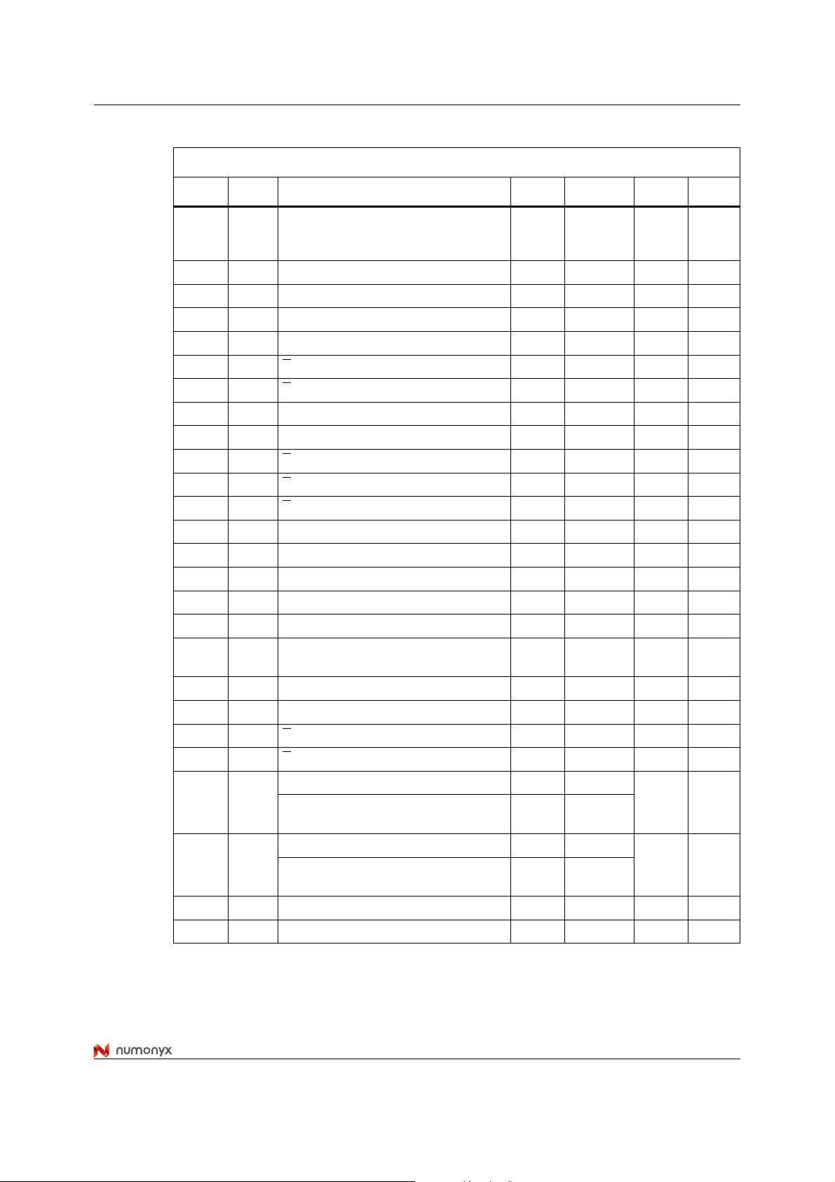
Table 12. AC characteristics (25 MHz operation)
Test conditions specified in Table 8 and Table 9
Symbol Alt. Parameter Min. Typ. Max. Unit
Clock frequency for the following
f
C
f
R
(1)
t
CH
(1)
t
CL
t
SLCH
t
CHSL
t
DVCH
t
CHDX
t
CHSH
t
SHCH
t
SHSL
t
SHQZ
t
CLQV
t
CLQX
t
RLRH
t
RHSL
t
SHRH
t
WHSL
t
SHWL
(2)
t
DP
t
RDP
(3)
t
PW
(3)
t
PP
t
PE
t
SE
1. tCH + tCL must be greater than or equal to 1/ fC(max).
2. Value guaranteed by characterization, not 100% tested in production.
3. When using PP and PW instructions to update consecutive bytes, optimized timings are obtained with one
sequence including all the bytes versus several sequences of only a few bytes (1 ≤ n ≤ 256).
(2)
(2)
(2)
f
instructions: FAST_READ, PW, PP, PE,
C
D.C. 25 MHz
SE, DP, RDP, WREN, WRDI, RDSR
Clock frequency for Read instructions D.C. 20 MHz
t
Clock High time 18 ns
CLH
t
Clock Low time 18 ns
CLL
(2)
Clock slew rate
t
S active setup time (relative to C) 10 ns
CSS
(peak to peak)
0.03 V/ns
S not active hold time (relative to C) 10 ns
t
Data in setup time 5 ns
DSU
t
Data in hold time 5 ns
DH
S active hold time (relative to C) 10 ns
S not active setup time (relative to C) 10 ns
t
S deselect time 200 ns
CSH
t
Output disable time 15 ns
DIS
t
Clock Low to Output valid 15 ns
V
t
Output hold time 0 ns
HO
t
Reset pulse width 10 µs
RST
t
Reset recovery time 3 µs
REC
Chip should have been deselected
before Reset is de-asserted
10 ns
Write protect setup time 50 ns
Write protect hold time 100 ns
S to deep power-down 3 µs
S High to standby power mode 30 µs
Page write cycle time (256 bytes) 11
Page write cycle time (n bytes)
10.2+
n*0.8/256
Page program cycle time (256 bytes) 1.2
Page program cycle time (n bytes)
0.4+
n*0.8/256
Page erase cycle time 10 20 ms
Sector erase cycle time 1 5 s
25 ms
5ms
37/47

DC and AC parameters M45PE10
Table 13. AC characteristics (33 MHz operation)
33 MHz only available for products marked since week 40 of 2005
Test conditions specified in Table 8 and Table 9
Symbol Alt. Parameter Min. Typ. Max. Unit
Clock frequency for the following
f
C
f
instructions: FAST_READ, PW, PP, PE,
C
D.C. 33 MHz
SE, DP, RDP, WREN, WRDI, RDSR
f
R
(2)
t
CH
(2)
t
CL
t
SLCH
t
CHSL
t
DVCH
t
CHDX
t
CHSH
t
SHCH
t
SHSLtCSH
(3)
t
SHQZ
t
CLQV
t
CLQX
t
THSL
t
SHTL
(3)
t
DP
(3)
t
RDP
Clock frequency for READ instructions D.C. 20 MHz
t
Clock High time 13 ns
CLH
t
Clock Low time 13 ns
CLL
(3)
Clock slew rate
t
S active setup time (relative to C) 10 ns
CSS
(peak to peak)
0.03 V/ns
S not active hold time (relative to C) 10 ns
t
Data in setup time 3 ns
DSU
t
Data in hold time 5 ns
DH
S active hold time (relative to C) 5 ns
S not active setup time (relative to C) 5 ns
S deselect time 200 ns
t
Output disable time 12 ns
DIS
tVClock Low to Output valid 12 ns
t
Output hold time 0 ns
HO
Top Sector Lock setup time 50 ns
Top Sector Lock hold time 100 ns
S to deep power-down 3 µs
S High to standby power mode 30 µs
Page write cycle time (256 bytes) 11
(4)
t
PW
Page write cycle time (n bytes)
10.2+
n*0.8/256
Page program cycle time (256 bytes) 1.2
(4)
t
PP
t
PE
t
SE
1. Details of how to find the date of marking are given in application note, AN1995.
2. tCH + tCL must be greater than or equal to 1/ fC.
3. Value guaranteed by characterization, not 100% tested in production.
4. When using PP and PW instructions to update consecutive bytes, optimized timings are obtained with one
sequence including all the bytes versus several sequences of only a few bytes (1 ≤ n ≤ 256).
Page program cycle time (n bytes)
Page erase cycle time 10 20 ms
Sector erase cycle time 1 5 s
0.4+
n*0.8/256
(1)
25 ms
5ms
38/47
M45PE10 DC and AC parameters
Table 14. AC char acteristics (50 MHz operation)
50 MHz operation for T9HX technology
(1)
Test conditions specified in Table 8 and Table 9
Symbol Alt. Parameter Min. T yp. Max. Unit
Clock frequency for the following instructions:
f
C
f
F AST_RE AD, PW, PP, PE, SE, DP, RDP,
C
D.C. 50 MHz
WREN, WRDI, RDSR, RDID
f
R
(2)
t
CH
(2)
t
CL
t
SLCHtCSS
t
CHSL
t
DVCHtDSU
t
CHDX
t
CHSH
t
SHCH
t
SHSL
(3)
t
SHQZ
t
CLQV
t
CLQX
t
WHSL
t
SHWL
(3)
t
DP
(3)
t
RDP
(3)
t
RLRH
t
RHSLtREC
t
SHRH
(4)
t
PW
(4)
t
PP
t
PE
t
SE
1. Delivery of parts in T9HX process to start from August 2007.
+ tCL must be greater than or equal to 1/ fC.
2. t
CH
3. Value guaranteed by characterization, not 100% tested in production.
4. n = number of bytes to program. int(A) corresponds to the upper integer part of A. Examples: int(1/8) = 1, int(16/8) = 2,
int(17/8) = 3.
Clock frequency for read instructions D.C. 33 MHz
t
Clock High time 9 ns
CLH
t
Clock Low time 9 ns
CLL
(3)
Clock slew rate
(peak to peak) 0.1 V/ns
S active setup time (relative to C) 5 ns
S not active hold time (relative to C) 5 ns
Data in setup time 2 ns
t
Data in hold time 5 ns
DH
S active hold time (relative to C) 5 ns
S not active setup time (relative to C) 5 ns
t
S deselect time 100 ns
CSH
t
Output disable time 8 ns
DIS
tVClock Low to Output valid 8 ns
t
Output hold time 0 ns
HO
Write protect setup time 50 ns
Write protect hold time 100 ns
S to deep power-down 3 µs
S High to standby mode 30 µs
t
Reset pulse width 10 µs
RST
Reset recovery time 3 µs
Chip should have been deselected before
Reset is de-asserted
10 ns
Page write cycle time (256 bytes) 11 23 ms
Page program cycle time (256 bytes) 0.8
3ms
Page program cycle time (n bytes) int(n/8) × 0.025
Page erase cycle time 10 20 ms
Sector erase cycle time 1.5 5 s
39/47

DC and AC parameters M45PE10
Table 15. AC char acteristics (75 MHz operation, T9HX (0.11 µm) process
(1))(2)
Test conditions specified in Table 8 and Table 9
Symbol Alt. Parameter Min. Typ. Max. Unit
Clock frequency for the following instructions:
f
f
C
FAST_READ, PW, PP, PE, SE, DP, RDP,
C
D.C. 75 MHz
WREN, WRDI, RDSR, RDID
f
R
(3)
t
CH
(3)
t
CL
t
SLCH
t
CHSL
t
DVCH
t
CHDX
t
CHSH
t
SHCH
t
SHSL
(4)
t
SHQZ
t
CLQV
t
CLQX
(5)
t
WHSL
(5)
t
SHWL
(3)
t
DP
(3)
t
RDP
t
W
(6)
t
PW
(6)
t
PP
t
PE
t
SE
t
SSE
t
BE
1. See Important note on page 6.
2. Details of how to find the technology process in the marking are given in AN1995, see also Section 12: Ordering
information.
+ tCL must be greater than or equal to 1/ fC.
3. t
CH
4. Value guaranteed by characterization, not 100% tested in production.
5. Only applicable as a constraint for a WRSR instruction when SRWD is set to ‘1’.
6. When using PP and PW instructions to update consecutive bytes, optimized timings are obtained with one sequence
including all the bytes versus several sequences of only a few bytes (1 ≤ n ≤ 256).
7. int(A) corresponds to the upper integer part of A. For instance, int(12/8) = 2, int(32/8) = 4 int(15.3) =16.
Clock frequency for read instructions D.C. 33 MHz
t
Clock High time 6 ns
CLH
t
Clock Low time 6 ns
CLL
Clock slew rate
t
S active setup time (relative to C) 5 ns
CSS
(3)
(peak to peak) 0.1 V/ns
S not active hold time (relative to C) 5 ns
t
Data in setup time 2 ns
DSU
t
Data in hold time 5 ns
DH
S active hold time (relative to C) 5 ns
S not active setup time (relative to C) 5 ns
t
S deselect time 100 ns
CSH
t
Output disable time 8 ns
DIS
t
Clock Low to Output valid 8 ns
V
t
Output hold time 0 ns
HO
Write protect setup time 20 ns
Write protect hold time 100 ns
S to deep power-down 3 µs
S High to standby mode 30 µs
Write status register cycle time 3 15 ms
Page write cycle time (256 bytes) 11 23 ms
Page program cycle time (256 bytes) 0.8
Page program cycle time (n bytes) int(n/8) × 0.025
(7)
Page erase cycle time 10 20 ms
Sector erase cycle time 1.5 5 s
Subsector erase cycle time 80 150 ms
Bulk erase cycle time 4.5 10 s
3ms
40/47
M45PE10 DC and AC parameters
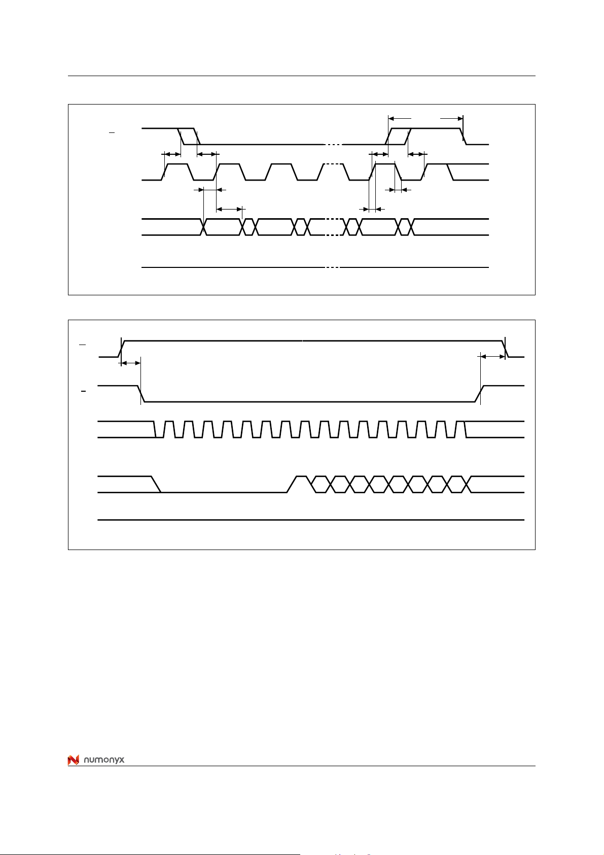
Figure 20. Serial input timing
tSHSL
S
tSLCH
C
tDVCH
tCHSHtCHSL
tSHCH
tCHCL
tCHDX
D
Q
MSB IN
High Impedance
Figure 21. Write Protect setup and hold timing
W
tWHSL
S
C
D
tCLCH
LSB IN
AI01447C
tSHWL
High Impedance
Q
AI07439
41/47

DC and AC parameters M45PE10
Figure 22. Output timing
S
tCH
C
tCLQV
tCLQV
tCL
tSHQZ
tCLQX
Q
ADDR.LSB IN
D
tCLQX
Figure 23. Reset AC waveforms
S
Reset
LSB OUT
tQLQH
tQHQL
AI01449e
tRHSLtSHRH
tRLRH
AI06808
42/47
M45PE10 Package mechanical
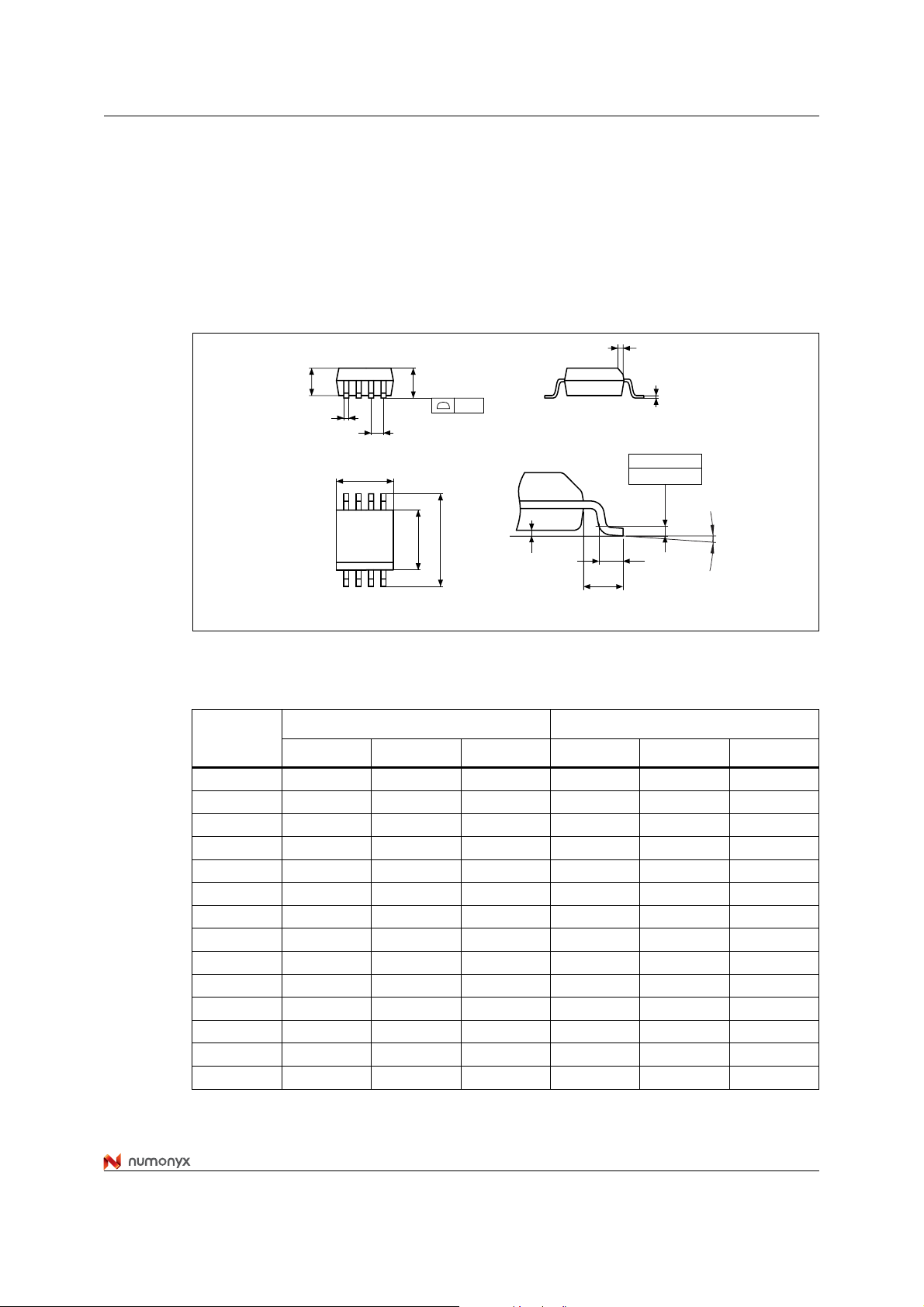
11 Package mechanical
In order to meet environmen tal requir ements , Numon yx offers these devices in ECOPACK®
packages. ECOPACK® packages are lead-free. The category of second level interconnect
is marked on the package and on the inner box label, in compliance with JEDEC Standard
JESD97. The maximum ratings related to soldering conditions are also marked on the inner
box label.
Figure 24. SO8N – 8 lead plastic small outline, 150 mils body width, package outline
h x 45˚
A2
b
e
D
8
1
1. Drawing is not to scale.
Table 16. SO8N – 8 lead plastic small outline, 150 mils body width, package
E1
A
ccc
E
A1
L
L1
c
0.25 mm
GAUGE PLANE
k
SO-A
mechanical data
Symbol
Typ Min Max Typ Min Max
A1.750.069
A1 0.10 0.25 0.004 0.010
A2 1.25 0.049
b 0.28 0.48 0.011 0.019
c 0.17 0.23 0.007 0.009
ccc 0.10 0.004
D 4.90 4.80 5.00 0.193 0.189 0.197
E 6.00 5.80 6.20 0.236 0.228 0.244
E1 3.90 3.80 4.00 0.154 0.150 0.157
e1.27– –0.050– –
h 0.25 0.50 0.010 0.020
k0°8°0°8°
L 0.40 1.27 0.016 0.050
L1 1.04 0.041
millimeters inches
43/47
Package mechanical M45PE10
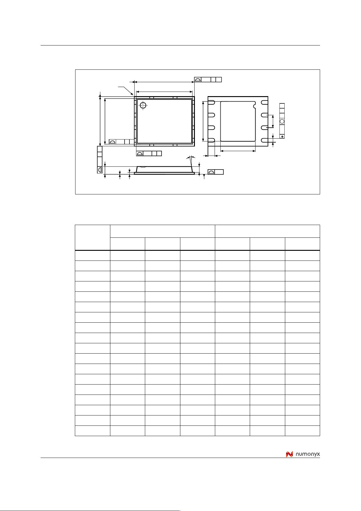
Figure 25. MLP8, 8-lead very thin dual flat package no lead, 6 × 5 mm, package
outline
θ
aaa CA
A2
C
ddd
CAB
eE2
M
bbb
b
D2
L
70-ME
A
R1
B
E
E1
2x
0.10 CB
0.10 CA
aaa CB
A
A1
A3
1. Drawing is not to scale.
Table 17. MLP8, 8-lead very thin dual flat package no lead, 6 × 5 mm, package
D
D1
mechanical data
millimeters inches
Symbol
Typ Min Max Typ Min Max
A 0.85 0.80 1.00 0.033 0.031 0.039
A1 0.00 0.05 0.000 0.002
A2 0.65 0.026
A3 0.20 0.008
b 0.40 0.35 0.48 0.016 0.014 0.019
D6.00 0.236
D1 5.75 0.226
D2 3.40 3.20 3.60 0.134 0.126 0.142
E5.00 0.197
E1 4.75 0.187
E2 4.00 3.80 4.30 0.157 0.150 0.169
e1.27– –0.050– –
R1 0.10 0.00 0.004 0.000
L 0.60 0.50 0.75 0.024 0.020 0.029
Θ 12° 12°
aaa 0.15 0.006
bbb 0.10 0.004
ddd 0.05 0.002
44/47

M45PE10 Ordering information
12 Ordering information
Table 18. Ordering information scheme
Example: M45PE10 – V MP 6 T G
Device type
M45PE = serial flash memory for data storage
Device function
10 = 1-Mbit (128 Kbit × 8)
Operating voltage
V = V
Package
MN = SO8 (150 mil width)
MP = VDFPN8 6 × 5 mm (MLP8)
Device grade
6 = Industrial temperature range, –40 to 85 °C.
Device tested with standard test flow
Option
blank = standard packing
T = tape and reel packing
Plating technology
P or G = ECOPACK® (RoHS compliant)
= 2.7 V to 3.6 V
CC
For a list of available options (speed, package, etc.), f or f urther information on any aspect of
this device or when ordering parts operating at 75 MHz (0.11 µm technology, process digit
‘4’), please contact your nearest Numonyx sales office.
45/47

Revision history M45PE10
13 Revision history
Table 19. Document revision history
Date Version Changes
29-Apr-2003 1.0 Initial release.
04-Jun-2003 1.1
04-Dec-2003 1.2
Description corrected of entering hardware protected mode (W must be
driven, and cannot be left unconnected).
V
(min) extended to –0.6 V, tPW(typ) and tPP(typ) improved. Table of
IO
contents, warning about exposed paddle on MLP8, and lead-free
options added. Change of naming for VDFPN8 package.
25-Jun-2004 1.3
Soldering temperature information clarified for RoHS compliant devices.
Device grade clarified.
22-Sep-2004 2.0 Document promoted to preliminary data. Minor wording changes
08-Oct-2004 3.0 Document promoted to mature datasheet. No other changes
Added AC characteristics (33 MHz operation). An easy way to modify
data, A fast way to modify data, P age write (PW) and Page program
4-Oct-2005 4.0
(PP) sections updated to explain optimal use of page write and page
program instructions. Updated I
values in Table 11: DC
CC3
characteristics. Updated T ab le 18: Ordering information scheme. Added
ECOPACK® information.
Document reformatted. 50 MHz frequency added (Table 14 added).
VCC supply voltage and VSS ground descriptions added.
Figure 4: SPI modes supported modified and explanatory text added.
VIO max modified in Table 7: Absolute maximum ratings.
02-Feb-2007 5
At power-up, The write in progress (WIP) bit is reset
end timing line modified in Figure 22: Output timing.
t
SHQZ
Blank option removed below Plating technology in Table 18: Ordering
information scheme. Small text changes.
Package specifications updated (see Section 11: Package mechanical).
Removed ‘low voltage’ from the title.
Updated the value for the maximum clock frequency (from 50 to
75 MHz) through the document.
Added: Table 15: AC characteristics (75 MHz operation, T9HX (0.11
21-Feb-2008 6
µm) process) and ECOPACK® text in Section 11: Package mechanical.
Modified: Table 11: DC characteristics, Figure 3: Bus master and
memory devices on the SPI bus, and Section 6.3: Read identification
(RDID).
Minor text changes.
01-Apr-2008 7 Applied Numonyx branding.
46/47

M45PE10
Please Read Carefully:
INFORMATION IN THIS DOCUMENT IS PROVIDED IN CONNECTION WITH NUMONYX™ PRODUCTS. NO LICENSE, EXPRESS OR
IMPLIED, BY ESTOPPEL OR OTHERWISE, TO ANY INTELLECTUAL PROPERTY RIGHTS IS GRANTED BY THIS DOCUMENT. EXCEPT
AS PROVIDED IN NUMONYX'S TERMS AND CONDITIONS OF SALE FOR SUCH PRODUCTS, NUMONYX ASSUMES NO LIABILITY
WHATSOEVER, AND NUMONYX DISCLAIMS ANY EXPRESS OR IMPLIED WARRANTY, RELATING TO SALE AND/OR USE OF
NUMONYX PRODUCTS INCLUDING LIABILITY OR WARRANTIES RELATING TO FITNESS FOR A PARTICULAR PURPOSE,
MERCHANTABILITY, OR INFRINGEMENT OF ANY PATENT, COPYRIGHT OR OTHER INTELLECTUAL PROPERTY RIGHT.
Numonyx products are not intended for use in medical, life saving, life sustaining, critical control or safety systems, or in nuclear facility
Numonyx may make changes to specificati ons and product descriptions at any time, without notice.
Numonyx, B.V. may have patents or pending patent applications, trademarks, copyrights, or other intellectual property rights that relate to the
presented subject matter. The furnishing of documents and other materials and information does not provide any license, express or implied,
by estoppel or otherwise, to any such patents, trademarks, copyrights, or other intellectual property rights.
Designers must not rely on the absence or characteristics of any features or instructions marked “reserved” or “undefined.” Numonyx reserves
these for future definition and shall have no responsibility whatsoever for conflicts or incompatibilities arising from future changes to them.
Contact your local Numonyx sale s office or your distributor to obtain the latest specifications and before placing your product order.
Copies of documents which have an order number and are referenced in this document, or other Numonyx literature may be obtained by
visiting Numonyx's website at http://www.numonyx.com.
Numonyx StrataFlash is a trademar k or registered trademark of Numonyx or its subsidiaries in the Uni ted States and other countries.
*Other names and brands may be claimed as the property of others.
Copyright © 11/5/7, Numonyx, B.V., All Rights Reserved.
applications.
47/47
 Loading...