


查询M36L0T7050B2供应商
128 Mbit (Multiple Bank, Multi-Level, Burst) Flash memory
and 32 Mbit (2Mb x16) PSRAM, Multi-Chip Package
Feature summary
■ Multi-Chip Package
– 1 die of 128 Mbit (8Mb x16, Multiple Bank,
Multi-level, Burst) Flash Memory
– 1 die of 32 Mbit (2Mb x16) Pseudo SRAM
■ Supply voltage
–V
–V
–V
■ Electronic signature
– Manufacturer Code: 20h
– Device Code (Top Flash Configuration)
– Device Code (Bottom Flash Configuration)
■ ECOPACK® packages available
Flash memory
■ Synchronous / Asynchronous Read
– Synchronous Burst Read mode: 52MHz
– Random Access: 85ns
■ Synchronous Burst Read Suspend
■ Programming time
– 2.5µs typical Word program time using
■ Memory organization
– Multiple Bank Memory Array: 8 Mbit Banks
– Parameter Blocks (Top or Bottom location)
■ Dual operations
– program/erase in one Bank while read in
– No delay between read and write
= 1.7 to 1.95V
DDF
= V
CCP
= 9V for fast program
PPF
= 2.7 to 3.1V
DDQ
M36L0T7050T2: 88C4h
M36L0T7050B2: 88C5h
Buffer Enhanced Factory Program
command
others
operations
M36L0T7050T2
M36L0T7050B2
Preliminary Data
FBGA
TFBGA88 (ZAQ)
8 x 10mm
■ Block locking
– All blocks locked at power-up
– Any combination of blocks can be locked
with zero latency
–WP
– Absolute Write Protection with V
■
Security
– 64 bit unique device number
– 2112 bit user programmable OTP Cells
■ Common Flash Interface (CFI)
■ 100,000 program/erase cycles per block
PSRAM
■ Access time: 65ns
■ 8-Word Page Access capability: 18ns
■ Low standby current: 100µA
■ Deep power down current: 10µA
■ Compatible with standard LPSRAM
■ Power-down modes
– Deep Power-Down
– 4 Mbit Partial Array Refresh
– 8 Mbit Partial Array Refresh
for Block Lock-Down
PP
= V
SS
November 2007 Rev 0.2 1/22
This is preliminary information on a new product now in development or undergoing evaluation. Details are subject to
change without notice.
www.numonyx.com
1

Contents M36L0T7050T2, M36L0T7050B2
Contents
1 Summary description . . . . . . . . . . . . . . . . . . . . . . . . . . . . . . . . . . . . . . . . 6
2 Signal descriptions . . . . . . . . . . . . . . . . . . . . . . . . . . . . . . . . . . . . . . . . . . 9
2.1 Address Inputs (A0-A22) . . . . . . . . . . . . . . . . . . . . . . . . . . . . . . . . . . . . . . 9
2.2 Data Input/Output (DQ0-DQ15) . . . . . . . . . . . . . . . . . . . . . . . . . . . . . . . . . 9
2.3 Flash Chip Enable (E
2.4 Flash Output Enable (G
2.5 Flash Write Enable (W
2.6 Flash Write Protect (WP
2.7 Flash Reset (RP
2.8 Flash Latch Enable (L
2.9 Flash Clock (K
) . . . . . . . . . . . . . . . . . . . . . . . . . . . . . . . . . . . . . . . . . . . . 10
F
2.10 Flash Wait (WAIT
) . . . . . . . . . . . . . . . . . . . . . . . . . . . . . . . . . . . . . . . 9
F
) . . . . . . . . . . . . . . . . . . . . . . . . . . . . . . . . . . . . . . 9
F
) . . . . . . . . . . . . . . . . . . . . . . . . . . . . . . . . . . . . . . 9
F
) . . . . . . . . . . . . . . . . . . . . . . . . . . . . . . . . . . . . 10
F
) . . . . . . . . . . . . . . . . . . . . . . . . . . . . . . . . . . . . . . . . . . 10
F
) . . . . . . . . . . . . . . . . . . . . . . . . . . . . . . . . . . . . . . 10
F
) . . . . . . . . . . . . . . . . . . . . . . . . . . . . . . . . . . . . . . . . . 10
F
2.11 PSRAM Chip Enable Input (E1
2.12 PSRAM Chip Enable Input (E2
2.13 PSRAM Write Enable (W
2.14 PSRAM Output Enable (G
) . . . . . . . . . . . . . . . . . . . . . . . . . . . . . . . . . . . 11
P
) . . . . . . . . . . . . . . . . . . . . . . . . . . . . . . . . . . 11
P
2.15 PSRAM Upper Byte Enable (UB
2.16 PSRAM Lower Byte Enable (LB
2.17 V
2.18 V
2.19 V
2.20 V
2.21 V
Supply Voltage . . . . . . . . . . . . . . . . . . . . . . . . . . . . . . . . . . . . . . . . 11
DDF
Supply Voltage . . . . . . . . . . . . . . . . . . . . . . . . . . . . . . . . . . . . . . . . 11
CCP
Supply Voltage . . . . . . . . . . . . . . . . . . . . . . . . . . . . . . . . . . . . . . . . 11
DDQ
Program Supply Voltage . . . . . . . . . . . . . . . . . . . . . . . . . . . . . . . . . 12
PPF
Ground . . . . . . . . . . . . . . . . . . . . . . . . . . . . . . . . . . . . . . . . . . . . . . . 12
SS
) . . . . . . . . . . . . . . . . . . . . . . . . . . . . . . . 10
P
) . . . . . . . . . . . . . . . . . . . . . . . . . . . . . . . 11
P
) . . . . . . . . . . . . . . . . . . . . . . . . . . . . . . 11
P
) . . . . . . . . . . . . . . . . . . . . . . . . . . . . . . 11
P
3 Functional description . . . . . . . . . . . . . . . . . . . . . . . . . . . . . . . . . . . . . . 13
4 Maximum rating . . . . . . . . . . . . . . . . . . . . . . . . . . . . . . . . . . . . . . . . . . . . 15
5 DC and AC parameters . . . . . . . . . . . . . . . . . . . . . . . . . . . . . . . . . . . . . . 16
6 Package mechanical . . . . . . . . . . . . . . . . . . . . . . . . . . . . . . . . . . . . . . . . 18
2/22

M36L0T7050T2, M36L0T7050B2 Contents
7 Part numbering . . . . . . . . . . . . . . . . . . . . . . . . . . . . . . . . . . . . . . . . . . . . 20
8 Revision history . . . . . . . . . . . . . . . . . . . . . . . . . . . . . . . . . . . . . . . . . . . 21
3/22

List of tables M36L0T7050T2, M36L0T7050B2
List of tables
Table 1. Signal names . . . . . . . . . . . . . . . . . . . . . . . . . . . . . . . . . . . . . . . . . . . . . . . . . . . . . . . . . . . . 7
Table 2. Operating modes . . . . . . . . . . . . . . . . . . . . . . . . . . . . . . . . . . . . . . . . . . . . . . . . . . . . . . . . 14
Table 3. Absolute maximum ratings . . . . . . . . . . . . . . . . . . . . . . . . . . . . . . . . . . . . . . . . . . . . . . . . . 15
Table 4. Operating and AC measurement conditions . . . . . . . . . . . . . . . . . . . . . . . . . . . . . . . . . . . . 16
Table 5. Device Capacitance . . . . . . . . . . . . . . . . . . . . . . . . . . . . . . . . . . . . . . . . . . . . . . . . . . . . . . 17
Table 6. Stacked TFBGA88 8x10mm - 8x10 active ball array, 0.8mm pitch, Package Data . . . . . . 19
Table 7. Ordering information scheme . . . . . . . . . . . . . . . . . . . . . . . . . . . . . . . . . . . . . . . . . . . . . . . 20
Table 8. Document revision history . . . . . . . . . . . . . . . . . . . . . . . . . . . . . . . . . . . . . . . . . . . . . . . . . 21
4/22

M36L0T7050T2, M36L0T7050B2 List of figures
List of figures
Figure 1. Logic diagram . . . . . . . . . . . . . . . . . . . . . . . . . . . . . . . . . . . . . . . . . . . . . . . . . . . . . . . . . . . . 6
Figure 2. TFBGA Connections (Top view through package) . . . . . . . . . . . . . . . . . . . . . . . . . . . . . . . . 8
Figure 3. Functional block diagram . . . . . . . . . . . . . . . . . . . . . . . . . . . . . . . . . . . . . . . . . . . . . . . . . . 13
Figure 4. AC Measurement I/O Waveform . . . . . . . . . . . . . . . . . . . . . . . . . . . . . . . . . . . . . . . . . . . . . 16
Figure 5. AC measurement load circuit . . . . . . . . . . . . . . . . . . . . . . . . . . . . . . . . . . . . . . . . . . . . . . . 17
Figure 6. Stacked TFBGA88 8x10mm - 8x10 active ball array, 0.8mm pitch,
Bottom View Outline . . . . . . . . . . . . . . . . . . . . . . . . . . . . . . . . . . . . . . . . . . . . . . . . . . . . . . 18
5/22
Summary description M36L0T7050T2, M36L0T7050B2
1 Summary description
The M36L0T7050T2 and M36L0T7050B2 combine two memory devices in a Multi-Chip
Package:
● a 128-Mbit, Multiple Bank, Multi-Level, Burst, Flash memory, the M58LT128HT or
M58LT128HB
● a 32-Mbit PseudoSRAM, the M69KW048BD.
The purpose of this document is to describe how the two memory components operate with
respect to each other. It should be read in conjunction with the M58LT128HTB and
M69KW048BD datasheets, where all specifications required to operate the Flash memory
and PSRAM components are fully detailed. These datasheets are available from your local
Numonyx distributor.
Recommended operating conditions do not allow more than one memory to be active at the
same time.
The memory is offered in a Stacked TFBGA88 (8 x 10mm, 8x10 ball array, 0.8mm pitch)
package. The devices are supplied with all the bits erased (set to ‘1’).
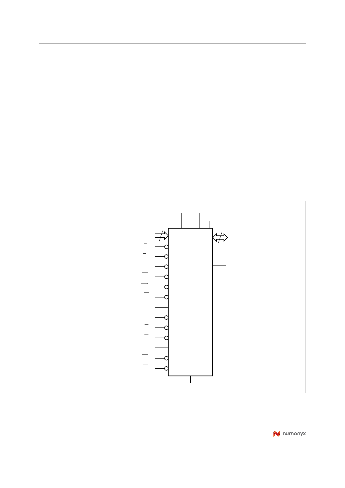
Figure 1. Logic diagram
A0-A22
E
G
W
RP
WP
L
K
E1
G
W
E2
UB
LB
V
DDQ
V
DDF
23
F
F
F
F
F
F
F
P
P
P
P
P
P
M36L0T7050T2
M36L0T7050B2
V
PPF
V
CCP
16
DQ0-DQ15
WAIT
F
6/22
V
SS
AI12878
M36L0T7050T2, M36L0T7050B2 Summary description
Table 1. Signal names
(1)
A0-A22
DQ0-DQ15 Common Data Input/Output
V
DDF
V
DDQ
V
PPF
V
SS
V
CCP
NC Not Connected Internally
DU Do Not Use as Internally Connected
Flash memory signals
L
F
E
F
G
F
W
F
RP
F
WP
F
Burst Clock
K
F
WAIT
F
PSRAM signals
E1
P
G
P
W
P
E2
P
UB
P
LB
P
1. A22-A21 are not connected to the PSRAM component.
Address Inputs
Power Supply for Flash Memory
Flash Memory Power Supply for I/O Buffers
Flash Optional Supply Voltage for Fast Program and Erase
Ground
PSRAM Power Supply
Latch Enable Input
Chip Enable Input
Output Enable Input
Write Enable Input
Reset Input
Write Protect Input
Wait Data in Burst Mode
Chip Enable Input
Output Enable Input
Write Enable Input
Power-down Input
Upper Byte Enable Input
Lower Byte Enable Input
7/22

Summary description M36L0T7050T2, M36L0T7050B2
Figure 2. TFBGA Connections (Top view through package)
87654321
A
B A21
C
D
E
F
G
H
DU
A4
A5
A3
A2
A1
A0
G
DU
A19A18
LB
P
A6
P
NC
NCA17
NCA7
UB
DQ1DQ0
V
SS
V
SS
V
PPF
WP
RP
P
DQ3
V
DDF
NC
W
P
L
F
F
F
W
F
DQ5DQ10DQ2DQ8
DQ12
NC
K
F
E
P
DQ13
DU
A22
A9
A10A20
A14A8
WAIT
DQ7DQ14
DU
A11
A12
A13
A15
A16
NC
F
NC
J
K
L
M
V
NC
E
DU
SS
DQ9G
F
F
DU DU NC
V
SS
DU
V
DDQ
8/22
DQ11
V
DDF
V
CCP
V
SS
NC
V
SS
DQ15DQ6DQ4
V
V
DDQ
SS
DU
V
E2
V
DDQ
P
SS
DU
AI08735b

M36L0T7050T2, M36L0T7050B2 Signal descriptions
2 Signal descriptions
See Figure 1: Logic diagram and Table 1: Signal names, for a brief overview of the signals
connected to this device.
2.1 Address Inputs (A0-A22)
Addresses A0-A20 are common inputs for the Flash memory and the PSRAM components.
The other lines (A21-A22) are inputs for the Flash memory component only.
The Address Inputs select the cells in the memory array to access during Bus Read
operations. During Bus Write operations they control the commands sent to the Command
Interface of the Program/Erase Controller in the Flash memory, and they select the cells to
be accessed in the PSRAM.
2.2 Data Input/Output (DQ0-DQ15)
In the Flash memory, the Data I/O outputs the data stored at the selected address during a
Bus Read operation or inputs a command or the data to be programmed during a Write Bus
operation.
In the PSRAM DQ0-DQ7 and/or DQ8-DQ15 carry the data to or from the upper and/or lower
part(s) of the selected address during a Write or Read operation, when Upper Byte Enable
(UB
) and/or Lower Byte Enable (LBP) is/are driven Low.
P
2.3 Flash Chip Enable (EF)
The Chip Enable input activates the memory control logic, input buffers, decoders and
sense amplifiers. When Chip Enable is Low, V
active mode. When Chip Enable is at V
high impedance and the power consumption is reduced to the standby level.
It is not allowed to set E
F
at V
E1P at VIL and E2P at V
IL,
2.4 Flash Output Enable (GF)
The Output Enable input controls data output during Flash memory Bus Read operations.
2.5 Flash Write Enable (WF)
The Write Enable controls the Bus Write operation of the Flash memories’ Command
Interface. The data and address inputs are latched on the rising edge of Chip Enable or
Write Enable whichever occurs first.
, and Reset is High, VIH, the device is in
IL
the Flash memory is deselected, the outputs are
IH
at the same time.
IH
9/22

Signal descriptions M36L0T7050T2, M36L0T7050B2
2.6 Flash Write Protect (WPF)
Write Protect is an input that gives an additional hardware protection for each block. When
Write Protect is Low, V
Down blocks cannot be changed. When Write Protect is at High, V
, Lock-Down is enabled and the protection status of the Locked-
IL
, Lock-Down is disabled
IH
and the Locked-Down blocks can be locked or unlocked. (See the Lock Status Table in the
M58LT128HTB datasheet).
2.7 Flash Reset (RPF)
The Reset input provides a hardware reset of the memory. When Reset is at VIL, the
memory is in Reset mode: the outputs are high impedance and the current consumption is
reduced to the Reset Supply Current I
of I
. After Reset all blocks are in the Locked state and the Configuration Register is
DD2
reset. When Reset is at V
, the device is in normal operation. Exiting Reset mode the
IH
device enters Asynchronous Read mode, but a negative transition of Chip Enable or Latch
Enable is required to ensure valid data outputs.
The Reset pin can be interfaced with 3V logic without any additional circuitry. It can be tied
to V
(refer to M58LT128HTB datasheet).
RPH
. Refer to M58LT128HTB datasheet for the value
DD2
2.8 Flash Latch Enable (LF)
Latch Enable latches the address bits on its rising edge. The address latch is transparent
when Latch Enable is Low, V
, and it is inhibited when Latch Enable is High, VIH. Latch
IL
Enable can be kept Low (also at board level) when the Latch Enable function is not required
or supported.
2.9 Flash Clock (KF)
The Clock input synchronizes the Flash memory to the microcontroller during synchronous
read operations; the address is latched on a Clock edge (rising or falling, according to the
configuration settings) when Latch Enable is at V
Read and in write operations.
2.10 Flash Wait (WAITF)
WAIT is a Flash output signal used during Synchronous Read to indicate whether the data
on the output bus are valid. This output is high impedance when Flash Chip Enable is at V
or Flash Reset is at V
cycle in advance. The WAIT
. It can be configured to be active during the wait cycle or one clock
IL
signal is not gated by Output Enable.
F
2.11 PSRAM Chip Enable Input (E1P)
. Clock is don't care during Asynchronous
IL
IH
When asserted (Low), the Chip Enable, E1P, activates the memory state machine, address
buffers and decoders, allowing Read and Write operations to be performed. When deasserted (High), all other pins are ignored, and the device is put, automatically, in low-power
Standby mode.
It is not allowed to set E
10/22
F
at V
E1P at VIL and E2P at V
IL,
at the same time.
IH

M36L0T7050T2, M36L0T7050B2 Signal descriptions
2.12 PSRAM Chip Enable Input (E2P)
The Chip Enable, E2P, puts the device in Deep Power-down mode when it is driven Low.
This is the lowest power mode.
2.13 PSRAM Write Enable (WP)
The Write Enable, WP, controls the Bus Write operation of the memory.
2.14 PSRAM Output Enable (GP)
The Output Enable, GP, provides a high speed tri-state control, allowing fast read/write
cycles to be achieved with the common I/O data bus.
2.15 PSRAM Upper Byte Enable (UBP)
The Upper Byte Enable, UBP, gates the data on the Upper Byte Data Inputs/Outputs (DQ8DQ15) to or from the upper part of the selected address during a Write or Read operation.
2.16 PSRAM Lower Byte Enable (LBP)
The Lower Byte Enable, LBP, gates the data on the Lower Byte Data Inputs/Outputs (DQ0DQ7) to or from the lower part of the selected address during a Write or Read operation.
2.17 V
V
the main power supply for all Flash operations (Read, Program and Erase).
2.18 V
The V
driving the refresh logic, even when the device is not being accessed.
2.19 V
V
powered independently of the Flash Memory core power supply, V
Supply Voltage
DDF
provides the power supply to the internal cores of the Flash memory component. It is
DDF
Supply Voltage
CCP
Supply Voltage supplies the power for all operations (Read or Write) and for
CCP
Supply Voltage
DDQ
provides the power supply for the Flash memory I/O pins. This allows all Outputs to be
DDQ
DDF
.
11/22

Signal descriptions M36L0T7050T2, M36L0T7050B2
2.20 V
V
Program Supply Voltage
PPF
is both a Flash control input and a Flash power supply pin. The two functions are
PPF
selected by the voltage range applied to the pin.
If V
is kept in a low voltage range (0V to V
PPF
case a voltage lower than V
while V
relevant values). V
PPF
> V
enables these functions (see the M58LT128HTB datasheet for the
PP1
PPF
PPLKF
is only sampled at the beginning of a Program or Erase; a change in
gives an absolute protection against Program or Erase,
DDQ
) V
is seen as a control input. In this
PPF
its value after the operation has started does not have any effect and Program or Erase
operations continue.
If V
is in the range of V
PPF
it acts as a power supply pin. In this condition V
PPH
stable until the Program/Erase algorithm is completed.
2.21 V
Ground
SS
VSS is the common ground reference for all voltage measurements in the Flash (core and
I/O Buffers) and PSRAM chips.
Note: The Flash memory device in a system should have their supply voltage (V
program supply voltage V
decoupled with a 0.1µF ceramic capacitor close to the pin
PPF
(high frequency, inherently low inductance capacitors should be as close as possible to the
package). See Figure 5: AC measurement load circuit. The PCB track widths should be
sufficient to carry the required V
program and erase currents.
PPF
) and the
DDF
must be
PPF
12/22

M36L0T7050T2, M36L0T7050B2 Functional description
3 Functional description
The PSRAM and Flash memory components have separate power supplies but share the
same grounds. They are distinguished by three Chip Enable inputs: E
memory and E1
and E2P for the PSRAM.
P
Recommended operating conditions do not allow more than one device to be active at a
time. The most common example is simultaneous read operations in the Flash memory and
the PSRAM which would result in a data bus contention. Therefore it is recommended to put
the other device in the high impedance state when reading the selected device.
Figure 3. Functional block diagram
for the Flash
F
A20-A22
A0-A19
W
RP
WP
E1
G
W
E2
UB
LB
Flash
Memory
16 Mbit
PSRAM
V
DDQ
DQ0-DQ15
WAIT
F
V
DDFVPPF
E
F
G
F
F
F
F
L
F
K
F
P
P
P
P
P
P
128 Mbit
V
CCP
V
SS
AI10965
13/22

Functional description M36L0T7050T2, M36L0T7050B2
Table 2. Operating modes
Operation E
Flash Read V
Flash Write V
Flash Address
Latch
Flash Output
Disable
GFW
F
ILVILVIHVIL
ILVIHVILVIL
VILXVIHVILV
V
ILVIHVIH
Flash Standby VIHXX X VIHHi-Z Hi-Z
Flash Reset X X X X V
(1)
LFRPFWAI T
F
(3)
(3)
XVIHHi-Z
(2)
E1PE2PGPWPLBP,UB
F
V
IH
V
IH
IH
PSRAM must be disabled
Any PSRAM mode is allowed
Hi-Z Hi-Z
IL
DQ0-
P
DQ7
Data Out
Data In
Data Out or Hi-Z
Hi-Z
DQ8-
DQ15
VILVIHVILVIHVILVIHdata out Hi-Z
PSRAM Read
(5)
Flash Memory must be disabled
V
ILVIHVILVIHVIHVIL
V
ILVIHVILVIHVILVIL
Hi-Z data out
data out
VILVIHVIHVILVILVIHdata in Hi-Z
PSRAM Write
PSRAM Output
Disabled
PSRAM Standby
(Deselected)
PSRAM Power-
(7)
Down
1. X = Don't care.
2. WAIT signal polarity is configured using the Set Configuration Register command. See the M58LT128HTB datasheet for
details.
can be tied to VIH if the valid address has been previously latched.
3. L
F
4. Depends on G
5. Should not be kept in this logic condition for a period longer than 1µs.
can be VIL during the Write operation if the following conditions are satisfied:
6. G
P
a. Write pulse is initiated by E1
b. G
7. Power-Down mode can be entered from Standby state and all Data outputs are in High-Z. The Power-Down current and
data retention depend on the selection of Power-Down programming.
(5)
(5)
Any Flash mode is allowed
.
F
(E1P Controlled Write timing), or cycle time of the previous operation cycle is satisfied;
stays VIL during the entire Write cycle.
P
P
V
ILVIHVIHVILVIHVIL
V
ILVIHVIH
V
ILVIH
V
IHVIH
(6)
VILVILV
VIHV
IL
VILV
VIHV
IH
XX X Hi-Z
Hi-Z data in
IL
IH
data in
Hi-Z
XVILXX X Hi-Z
(4)
14/22

M36L0T7050T2, M36L0T7050B2 Maximum rating
4 Maximum rating
Stressing the device above the rating listed in the Absolute Maximum Ratings table may
cause permanent damage to the device. These are stress ratings only and operation of the
device at these or any other conditions above those indicated in the Operating sections of
this specification is not implied. Exposure to Absolute Maximum Rating conditions for
extended periods may affect device reliability. Refer also to the Numonyx SURE Program
and other relevant quality documents.
Table 3. Absolute maximum ratings
Value
Symbol Parameter
Min Max
Unit
V
T
T
V
DDQ
V
t
VPPFH
T
A
BIAS
STG
V
IO
DDF
, V
PPF
I
O
Ambient Operating Temperature –25 85 °C
Temperature Under Bias –25 85 °C
Storage Temperature –55 125 °C
Input or Output Voltage –0.5 3.6 V
Flash Memory Core Supply Voltage –0.2 2.5 V
PSRAM and Input/Output Supply
CCP
Voltages
–0.2 3.6 V
Flash Program Voltage –0.2 10 V
Output Short Circuit Current – 100 mA
Time for V
PPF
at V
PPFH
100 hours
15/22

DC and AC parameters M36L0T7050T2, M36L0T7050B2
5 DC and AC parameters
This section summarizes the operating measurement conditions, and the DC and AC
characteristics of the device. The parameters in the DC and AC characteristics Tables that
follow, are derived from tests performed under the Measurement Conditions summarized in
Table 4: Operating and AC measurement conditions. Designers should check that the
operating conditions in their circuit match the operating conditions when relying on the
quoted parameters.
Table 4. Operating and AC measurement conditions
Flash Memories PSRAM
Parameter
Min Max Min Max
V
Supply Voltage 1.7 1.95 – – V
DDF
Supply Voltage – – 2.7 3.1 V
V
CCP
V
Supply Voltage 2.7 3.1 – – V
DDQ
V
Supply Voltage (Factory environment) 8.5 9.5 – – V
PPF
V
Supply Voltage (Application
PPF
environment)
–0.4 V
+0.4 – – V
DDQ
Ambient Operating Temperature –25 85 –30 85 °C
Unit
Load Capacitance (C
Output Circuit Resistors (R
)3050pF
L
, R2)2222kΩ
1
Input Rise and Fall Times 5 5 ns
Input Pulse Voltages 0 to V
Input and Output Timing Ref. Voltages V
DDQ
DDQ
/2 V
0 to V
DDQ
DDQ
/2 V
Figure 4. AC Measurement I/O Waveform
V
DDQ
V
/2
DDQ
0V
AI06161
V
16/22

M36L0T7050T2, M36L0T7050B2 DC and AC parameters
Figure 5. AC measurement load circuit
V
DDQ
V
0.1µF
Table 5. Device Capacitance
DDF
V
0.1µF
DDQ
DEVICE
UNDER
TEST
includes JIG capacitance
C
L
(1)
CL
R
1
R
2
AI08364B
Symbol Parameter Test Condition Min Max Unit
C
IN
C
OUT
1. Sampled only, not 100% tested.
Input Capacitance VIN = 0V 12 pF
Output Capacitance V
= 0V 15 pF
OUT
Please refer to the M58LT128HTB and M69KW048BD datasheets for further DC and AC
characteristic values and illustrations.
17/22

Package mechanical M36L0T7050T2, M36L0T7050B2
6 Package mechanical
In order to meet environmental requirements, Numonyx offers these devices in ECOPACK®
packages. These packages have a Lead-free second-level interconnect. The category of
Second-Level Interconnect is marked on the package and on the inner box label, in
compliance with JEDEC Standard JESD97.
The maximum ratings related to soldering conditions are also marked on the inner box label.
Figure 6. Stacked TFBGA88 8x10mm - 8x10 active ball array, 0.8mm pitch,
Bottom View Outline
D
D1
E
E2
E1
FE FE1
1. Drawing is not to scale.
SE
BALL "A1"
A
FD
e
b
ddd
SD
A2
A1
BGA-Z42
18/22

M36L0T7050T2, M36L0T7050B2 Package mechanical
Table 6. Stacked TFBGA88 8x10mm - 8x10 active ball array, 0.8mm pitch, Package Data
millimeters inches
Symbol
Typ Min Max Typ Min Max
A 1.200 0.0472
A1 0.200 0.0079
A2 0.850 0.0335
b 0.350 0.300 0.400 0.0138 0.0118 0.0157
D 8.000 7.900 8.100 0.3150 0.3110 0.3189
D1 5.600 0.2205
ddd 0.100 0.0039
E 10.000 9.900 10.100 0.3937 0.3898 0.3976
E1 7.200 0.2835
E2 8.800 0.3465
e 0.800 – – 0.0315 – –
FD 1.200 0.0472
FE 1.400 0.0551
FE1 0.600 0.0236
SD 0.400 0.0157
SE 0.400 0.0157
19/22

Part numbering M36L0T7050T2, M36L0T7050B2
7 Part numbering
Table 7. Ordering information scheme
Example: M36 L 0 T 7 0 5 0 T 2 ZAQ F
Device Type
M36 = Multi-Chip Package (Flash + RAM)
Flash 1 Architecture
L = Multilevel, Multiple Bank, Burst mode
Flash 2 Architecture
0 = No Die
Operating Voltage
T = V
= 1.7 to 1.95V; V
DDF
Flash 1 Density
7 = 128 Mbit
DDQ
= V
= 2.7 to 3.1V
CCP
Flash 2 Density
0 = No Die
RAM 1 Density
5 = 32 Mbit
RAM 0 Density
0 = No Die
Parameter Blocks Location
T = Top Boot Block Flash
B = Bottom Boot Block Flash
Product Version
2 = 90nm Flash technology and Multi-Level design, 85ns speed; 0.13µm RAM, 65ns
speed
Package
ZAQ = Stacked TFBGA88 8x10mm - 8x10 active ball array, 0.8mm pitch
Option
Blank = Standard Packing
T = Tape & Reel Packing
E = ECOPACK® package, standard packing
F = ECOPACK® package, tape and reel packing
Devices are shipped from the factory with the memory content bits erased to ’1’. For a list of
available options (Speed, Package, etc.) or for further information on any aspect of this
device, please contact the Numonyx Sales Office nearest to you.
20/22

M36L0T7050T2, M36L0T7050B2 Revision history
8 Revision history
Table 8. Document revision history
Date Revision Changes
04-May-2006 01 Initial release.
13-Nov-2007 02 Applied Numonyx branding.
21/22

M36L0T7050T2, M36L0T7050B2
Please Read Carefully:
INFORMATION IN THIS DOCUMENT IS PROVIDED IN CONNECTION WITH NUMONYX™ PRODUCTS. NO LICENSE, EXPRESS OR
IMPLIED, BY ESTOPPEL OR OTHERWISE, TO ANY INTELLECTUAL PROPERTY RIGHTS IS GRANTED BY THIS DOCUMENT. EXCEPT
AS PROVIDED IN NUMONYX'S TERMS AND CONDITIONS OF SALE FOR SUCH PRODUCTS, NUMONYX ASSUMES NO LIABILITY
WHATSOEVER, AND NUMONYX DISCLAIMS ANY EXPRESS OR IMPLIED WARRANTY, RELATING TO SALE AND/OR USE OF
NUMONYX PRODUCTS INCLUDING LIABILITY OR WARRANTIES RELATING TO FITNESS FOR A PARTICULAR PURPOSE,
MERCHANTABILITY, OR INFRINGEMENT OF ANY PATENT, COPYRIGHT OR OTHER INTELLECTUAL PROPERTY RIGHT.
Numonyx products are not intended for use in medical, life saving, life sustaining, critical control or safety systems, or in nuclear facility
Numonyx may make changes to specifications and product descriptions at any time, without notice.
Numonyx, B.V. may have patents or pending patent applications, trademarks, copyrights, or other intellectual property rights that relate to the
presented subject matter. The furnishing of documents and other materials and information does not provide any license, express or implied,
by estoppel or otherwise, to any such patents, trademarks, copyrights, or other intellectual property rights.
Designers must not rely on the absence or characteristics of any features or instructions marked “reserved” or “undefined.” Numonyx reserves
these for future definition and shall have no responsibility whatsoever for conflicts or incompatibilities arising from future changes to them.
Contact your local Numonyx sales office or your distributor to obtain the latest specifications and before placing your product order.
Copies of documents which have an order number and are referenced in this document, or other Numonyx literature may be obtained by
visiting Numonyx's website at http://www.numonyx.com.
Numonyx StrataFlash is a trademark or registered trademark of Numonyx or its subsidiaries in the United States and other countries.
*Other names and brands may be claimed as the property of others.
Copyright © 11/5/7, Numonyx, B.V., All Rights Reserved.
applications.
22/22
 Loading...