

Page 1
512-Kbit, serial flash memory, 50 MHz SPI bus interface
Features
■ 512 Kbits of flash memory
■ Page program (up to 256 bytes) in 1.4 ms
(typical)
■ Sector erase (256 Kbits) in 0.65 s (typical)
■ Bulk erase (512 Kbits) in 0.85 s (typical)
■ 2.3 to 3.6 V single supply voltage
■ SPI bus compatible serial interface
■ 50 MHz clock rate (maximum)
■ Deep power-down mode 1 µA (typical)
■ Electronic signatures
– JEDEC standard two-byte signature
(2010h)
– RES instruction, one-byte, signature (05h),
for backward compatibility
■ More than 100,000 erase/program cycles per
sector
■ More than 20 years data retention
■ ECOPACK® packages available
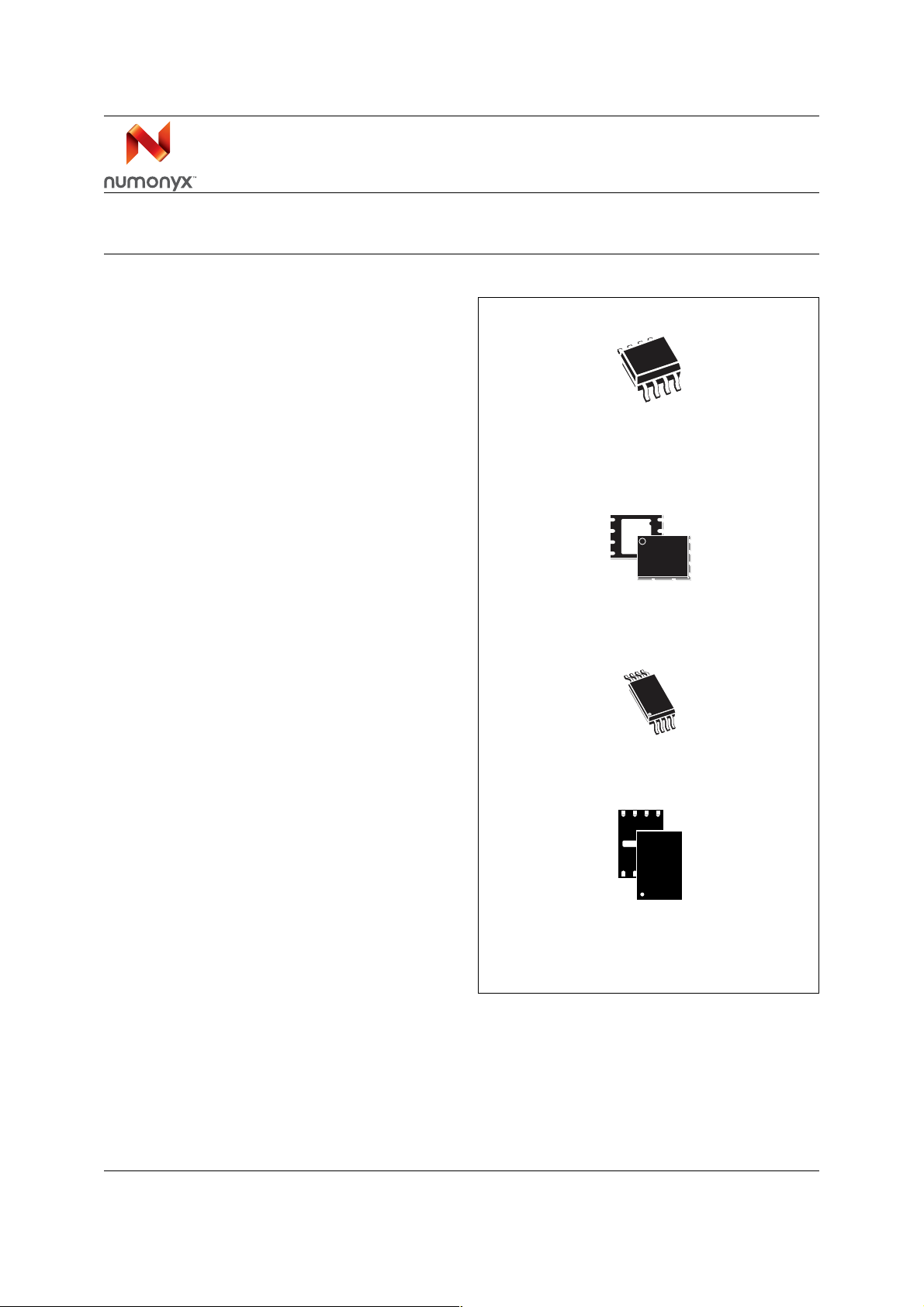
M25P05-A
SO8 (MN)
150 mil width
VFQFPN8 (MP)
(MLP8)
TSSOP8 (DW)
UFDFPN8 (MB)
2x3mm
April 2008 Rev 11 1/52
www.numonyx.com
1
Page 2

Contents M25P05-A
Contents
1 Description . . . . . . . . . . . . . . . . . . . . . . . . . . . . . . . . . . . . . . . . . . . . . . . . . 6
2 Signal descriptions . . . . . . . . . . . . . . . . . . . . . . . . . . . . . . . . . . . . . . . . . . 8
2.1 Serial Data output (Q) . . . . . . . . . . . . . . . . . . . . . . . . . . . . . . . . . . . . . . . . 8
2.2 Serial Data input (D) . . . . . . . . . . . . . . . . . . . . . . . . . . . . . . . . . . . . . . . . . . 8
2.3 Serial Clock (C) . . . . . . . . . . . . . . . . . . . . . . . . . . . . . . . . . . . . . . . . . . . . . 8
2.4 Chip Select (S
2.5 Hold (HOLD
2.6 Write Protect (W
2.7 V
2.8 V
supply voltage . . . . . . . . . . . . . . . . . . . . . . . . . . . . . . . . . . . . . . . . . . . 9
CC
ground . . . . . . . . . . . . . . . . . . . . . . . . . . . . . . . . . . . . . . . . . . . . . . . . . 9
SS
) . . . . . . . . . . . . . . . . . . . . . . . . . . . . . . . . . . . . . . . . . . . . . . 8
) . . . . . . . . . . . . . . . . . . . . . . . . . . . . . . . . . . . . . . . . . . . . . . . . 8
) . . . . . . . . . . . . . . . . . . . . . . . . . . . . . . . . . . . . . . . . . . . . 8
3 SPI modes . . . . . . . . . . . . . . . . . . . . . . . . . . . . . . . . . . . . . . . . . . . . . . . . 10
4 Operating features . . . . . . . . . . . . . . . . . . . . . . . . . . . . . . . . . . . . . . . . . 12
4.1 Page programming . . . . . . . . . . . . . . . . . . . . . . . . . . . . . . . . . . . . . . . . . . 12
4.2 Sector erase and bulk erase . . . . . . . . . . . . . . . . . . . . . . . . . . . . . . . . . . 12
4.3 Polling during a write, program or erase cycle . . . . . . . . . . . . . . . . . . . . . 12
4.4 Active power, standby power and deep power-down modes . . . . . . . . . . 12
4.5 Status register . . . . . . . . . . . . . . . . . . . . . . . . . . . . . . . . . . . . . . . . . . . . . 13
4.5.1 WIP bit . . . . . . . . . . . . . . . . . . . . . . . . . . . . . . . . . . . . . . . . . . . . . . . . . . 13
4.5.2 WEL bit . . . . . . . . . . . . . . . . . . . . . . . . . . . . . . . . . . . . . . . . . . . . . . . . . 13
4.5.3 BP1, BP0 bits . . . . . . . . . . . . . . . . . . . . . . . . . . . . . . . . . . . . . . . . . . . . . 13
4.5.4 SRWD bit . . . . . . . . . . . . . . . . . . . . . . . . . . . . . . . . . . . . . . . . . . . . . . . . 13
4.6 Protection modes . . . . . . . . . . . . . . . . . . . . . . . . . . . . . . . . . . . . . . . . . . . 14
4.7 Hold condition . . . . . . . . . . . . . . . . . . . . . . . . . . . . . . . . . . . . . . . . . . . . . . 15
5 Memory organization . . . . . . . . . . . . . . . . . . . . . . . . . . . . . . . . . . . . . . . 16
6 Instructions . . . . . . . . . . . . . . . . . . . . . . . . . . . . . . . . . . . . . . . . . . . . . . . 18
6.1 Write enable (WREN) . . . . . . . . . . . . . . . . . . . . . . . . . . . . . . . . . . . . . . . . 19
6.2 Write disable (WRDI) . . . . . . . . . . . . . . . . . . . . . . . . . . . . . . . . . . . . . . . . 20
6.3 Read identification (RDID) . . . . . . . . . . . . . . . . . . . . . . . . . . . . . . . . . . . . 21
2/52
Page 3

M25P05-A Contents
6.4 Read status register (RDSR) . . . . . . . . . . . . . . . . . . . . . . . . . . . . . . . . . . 22
6.4.1 WIP bit . . . . . . . . . . . . . . . . . . . . . . . . . . . . . . . . . . . . . . . . . . . . . . . . . . 22
6.4.2 WEL bit . . . . . . . . . . . . . . . . . . . . . . . . . . . . . . . . . . . . . . . . . . . . . . . . . 22
6.4.3 BP1, BP0 bits . . . . . . . . . . . . . . . . . . . . . . . . . . . . . . . . . . . . . . . . . . . . . 22
6.4.4 SRWD bit . . . . . . . . . . . . . . . . . . . . . . . . . . . . . . . . . . . . . . . . . . . . . . . . 22
6.5 Write status register (WRSR) . . . . . . . . . . . . . . . . . . . . . . . . . . . . . . . . . . 23
6.6 Read data bytes (READ) . . . . . . . . . . . . . . . . . . . . . . . . . . . . . . . . . . . . . 26
6.7 Read data bytes at higher speed (FAST_READ) . . . . . . . . . . . . . . . . . . . 27
6.8 Page program (PP) . . . . . . . . . . . . . . . . . . . . . . . . . . . . . . . . . . . . . . . . . . 28
6.9 Sector erase (SE) . . . . . . . . . . . . . . . . . . . . . . . . . . . . . . . . . . . . . . . . . . . 30
6.10 Bulk erase (BE) . . . . . . . . . . . . . . . . . . . . . . . . . . . . . . . . . . . . . . . . . . . . 31
6.11 Deep power-down (DP) . . . . . . . . . . . . . . . . . . . . . . . . . . . . . . . . . . . . . . 32
6.12 Release from deep power-down and read electronic signature (RES) . . 33
7 Power-up and power-down . . . . . . . . . . . . . . . . . . . . . . . . . . . . . . . . . . . 35
8 Initial delivery state . . . . . . . . . . . . . . . . . . . . . . . . . . . . . . . . . . . . . . . . . 36
9 Maximum ratings . . . . . . . . . . . . . . . . . . . . . . . . . . . . . . . . . . . . . . . . . . . 37
10 DC and AC parameters . . . . . . . . . . . . . . . . . . . . . . . . . . . . . . . . . . . . . . 38
11 Package mechanical . . . . . . . . . . . . . . . . . . . . . . . . . . . . . . . . . . . . . . . . 45
12 Ordering information . . . . . . . . . . . . . . . . . . . . . . . . . . . . . . . . . . . . . . . 49
13 Revision history . . . . . . . . . . . . . . . . . . . . . . . . . . . . . . . . . . . . . . . . . . . 50
3/52
Page 4

List of tables M25P05-A
List of tables
Table 1. Signal names . . . . . . . . . . . . . . . . . . . . . . . . . . . . . . . . . . . . . . . . . . . . . . . . . . . . . . . . . . . . 6
Table 2. Protected area sizes. . . . . . . . . . . . . . . . . . . . . . . . . . . . . . . . . . . . . . . . . . . . . . . . . . . . . . 14
Table 3. Memory organization . . . . . . . . . . . . . . . . . . . . . . . . . . . . . . . . . . . . . . . . . . . . . . . . . . . . . 16
Table 4. Instruction set . . . . . . . . . . . . . . . . . . . . . . . . . . . . . . . . . . . . . . . . . . . . . . . . . . . . . . . . . . . 19
Table 5. Read identification (RDID) data-out sequence . . . . . . . . . . . . . . . . . . . . . . . . . . . . . . . . . . 21
Table 6. Status register format . . . . . . . . . . . . . . . . . . . . . . . . . . . . . . . . . . . . . . . . . . . . . . . . . . . . . 22
Table 7. Protection modes . . . . . . . . . . . . . . . . . . . . . . . . . . . . . . . . . . . . . . . . . . . . . . . . . . . . . . . . 25
Table 8. Power-up timing and VWI threshold . . . . . . . . . . . . . . . . . . . . . . . . . . . . . . . . . . . . . . . . . . 36
Table 9. Absolute maximum ratings . . . . . . . . . . . . . . . . . . . . . . . . . . . . . . . . . . . . . . . . . . . . . . . . . 37
Table 10. Operating conditions. . . . . . . . . . . . . . . . . . . . . . . . . . . . . . . . . . . . . . . . . . . . . . . . . . . . . . 38
Table 11. AC measurement conditions. . . . . . . . . . . . . . . . . . . . . . . . . . . . . . . . . . . . . . . . . . . . . . . . 38
Table 12. Capacitance . . . . . . . . . . . . . . . . . . . . . . . . . . . . . . . . . . . . . . . . . . . . . . . . . . . . . . . . . . . . 38
Table 13. DC characteristics. . . . . . . . . . . . . . . . . . . . . . . . . . . . . . . . . . . . . . . . . . . . . . . . . . . . . . . . 39
Table 14. Instruction times . . . . . . . . . . . . . . . . . . . . . . . . . . . . . . . . . . . . . . . . . . . . . . . . . . . . . . . . . 39
Table 15. AC characteristics (25 MHz operation). . . . . . . . . . . . . . . . . . . . . . . . . . . . . . . . . . . . . . . . 40
Table 16. AC characteristics (40 MHz operation). . . . . . . . . . . . . . . . . . . . . . . . . . . . . . . . . . . . . . . . 41
Table 17. AC characteristics (50 MHz operation). . . . . . . . . . . . . . . . . . . . . . . . . . . . . . . . . . . . . . . . 42
Table 18. SO8N – 8 lead plastic small outline, 150 mils body width, package mechanical data . . . . 45
Table 19. VFQFPN8 (MLP8) - 8 lead very thin fin e pitch quad flat package no lead,
6 × 5 mm, package mechanical data . . . . . . . . . . . . . . . . . . . . . . . . . . . . . . . . . . . . . . . . . 46
Table 20. TSSOP8 – 8 lead thin shrink small outline, package mechanical data. . . . . . . . . . . . . . . . 47
Table 21. UFDFPN8 (MLP8) – 8 lead ultra thin fine pitch dual flat package no lead,
2 x 3 mm package mechanical data . . . . . . . . . . . . . . . . . . . . . . . . . . . . . . . . . . . . . . . . . . 48
Table 22. Ordering information scheme . . . . . . . . . . . . . . . . . . . . . . . . . . . . . . . . . . . . . . . . . . . . . . . 49
Table 23. Document revision history . . . . . . . . . . . . . . . . . . . . . . . . . . . . . . . . . . . . . . . . . . . . . . . . . 50
4/52
Page 5

M25P05-A List of figures
List of figures
Figure 1. Logic diagram . . . . . . . . . . . . . . . . . . . . . . . . . . . . . . . . . . . . . . . . . . . . . . . . . . . . . . . . . . . . 6
Figure 2. SO, VFQFPN and TSSOP connections . . . . . . . . . . . . . . . . . . . . . . . . . . . . . . . . . . . . . . . . 7
Figure 3. Bus master and memory devices on the SPI bus. . . . . . . . . . . . . . . . . . . . . . . . . . . . . . . . 10
Figure 4. SPI modes supported . . . . . . . . . . . . . . . . . . . . . . . . . . . . . . . . . . . . . . . . . . . . . . . . . . . . . 11
Figure 5. Hold condition activation. . . . . . . . . . . . . . . . . . . . . . . . . . . . . . . . . . . . . . . . . . . . . . . . . . . 15
Figure 6. Block diagram. . . . . . . . . . . . . . . . . . . . . . . . . . . . . . . . . . . . . . . . . . . . . . . . . . . . . . . . . . . 17
Figure 7. Write enable (WREN) instruction sequence . . . . . . . . . . . . . . . . . . . . . . . . . . . . . . . . . . . . 19
Figure 8. Write disable (WRDI) instruction sequence . . . . . . . . . . . . . . . . . . . . . . . . . . . . . . . . . . . . 20
Figure 9. Read identification (RDID) instruction sequence and data-out sequence . . . . . . . . . . . . . 21
Figure 10. Read status register (RDSR) instruction sequence and data-out sequence . . . . . . . . . . . 23
Figure 11. Write status register (WRSR) instruction sequence . . . . . . . . . . . . . . . . . . . . . . . . . . . . . . 24
Figure 12. Read data bytes (READ) instruction sequence and data-out sequence . . . . . . . . . . . . . . 26
Figure 13. Read data bytes at higher speed (FAST_READ) instruction sequence
and data-out sequence . . . . . . . . . . . . . . . . . . . . . . . . . . . . . . . . . . . . . . . . . . . . . . . . . . . . 27
Figure 14. Page program (PP) instruction sequence. . . . . . . . . . . . . . . . . . . . . . . . . . . . . . . . . . . . . . 29
Figure 15. Sector erase (SE) instruction sequence . . . . . . . . . . . . . . . . . . . . . . . . . . . . . . . . . . . . . . . 30
Figure 16. Bulk erase (BE) instruction sequence. . . . . . . . . . . . . . . . . . . . . . . . . . . . . . . . . . . . . . . . . 31
Figure 17. Deep power-down (DP) instruction sequence . . . . . . . . . . . . . . . . . . . . . . . . . . . . . . . . . . 32
Figure 18. Release from deep power-down and read electronic signature (RES)
instruction sequence and data-out sequence . . . . . . . . . . . . . . . . . . . . . . . . . . . . . . . . . . 34
Figure 19. Release from deep power-down (RES) instruction sequence . . . . . . . . . . . . . . . . . . . . . . 34
Figure 20. Power-up timing . . . . . . . . . . . . . . . . . . . . . . . . . . . . . . . . . . . . . . . . . . . . . . . . . . . . . . . . . 36
Figure 21. AC measurement I/O waveform . . . . . . . . . . . . . . . . . . . . . . . . . . . . . . . . . . . . . . . . . . . . . 38
Figure 22. Serial input timing . . . . . . . . . . . . . . . . . . . . . . . . . . . . . . . . . . . . . . . . . . . . . . . . . . . . . . . . 43
Figure 23. Write protect setup and hold timing during WRSR when SRWD =1. . . . . . . . . . . . . . . . . . 43
Figure 24. Hold timing . . . . . . . . . . . . . . . . . . . . . . . . . . . . . . . . . . . . . . . . . . . . . . . . . . . . . . . . . . . . . 44
Figure 25. Output timing . . . . . . . . . . . . . . . . . . . . . . . . . . . . . . . . . . . . . . . . . . . . . . . . . . . . . . . . . . . 44
Figure 26. SO8N – 8 lead plastic small outline , 150 mils body width, package outline . . . . . . . . . . . . 45
Figure 27. VFQFPN8 (MLP8) - 8 lead very thin fine pitch quad flat package no lead,
6 × 5 mm, package outline . . . . . . . . . . . . . . . . . . . . . . . . . . . . . . . . . . . . . . . . . . . . . . . . . 46
Figure 28. TSSOP8 – 8 lead thin shrink small outline, package outline . . . . . . . . . . . . . . . . . . . . . . . 47
Figure 29. UFDFPN8 (MLP8) – 8 lead ultra thin fine pitch dual flat package no lead,
2 x 3 mm package outline. . . . . . . . . . . . . . . . . . . . . . . . . . . . . . . . . . . . . . . . . . . . . . . . . . 48
5/52
Page 6

Description M25P05-A
1 Description
The M25P05-A is a 512-Kbit (64 Kbits ×8) serial flash memory, with advanced write
protection mechanisms, accessed by a high speed SPI-compatible bus.
The memory can be programmed 1 to 256 bytes at a time, using the page program
instruction.
The memory is organized as 2 sectors, each co ntaini ng 128 pages. Each page is 256 bytes
wide. Thus, the whole memory can be viewed as consisting of 256 pages, or 65,536 bytes.
The whole memory can be erased using the bulk erase instruction, or a sector at a time,
using the sector erase instruction.
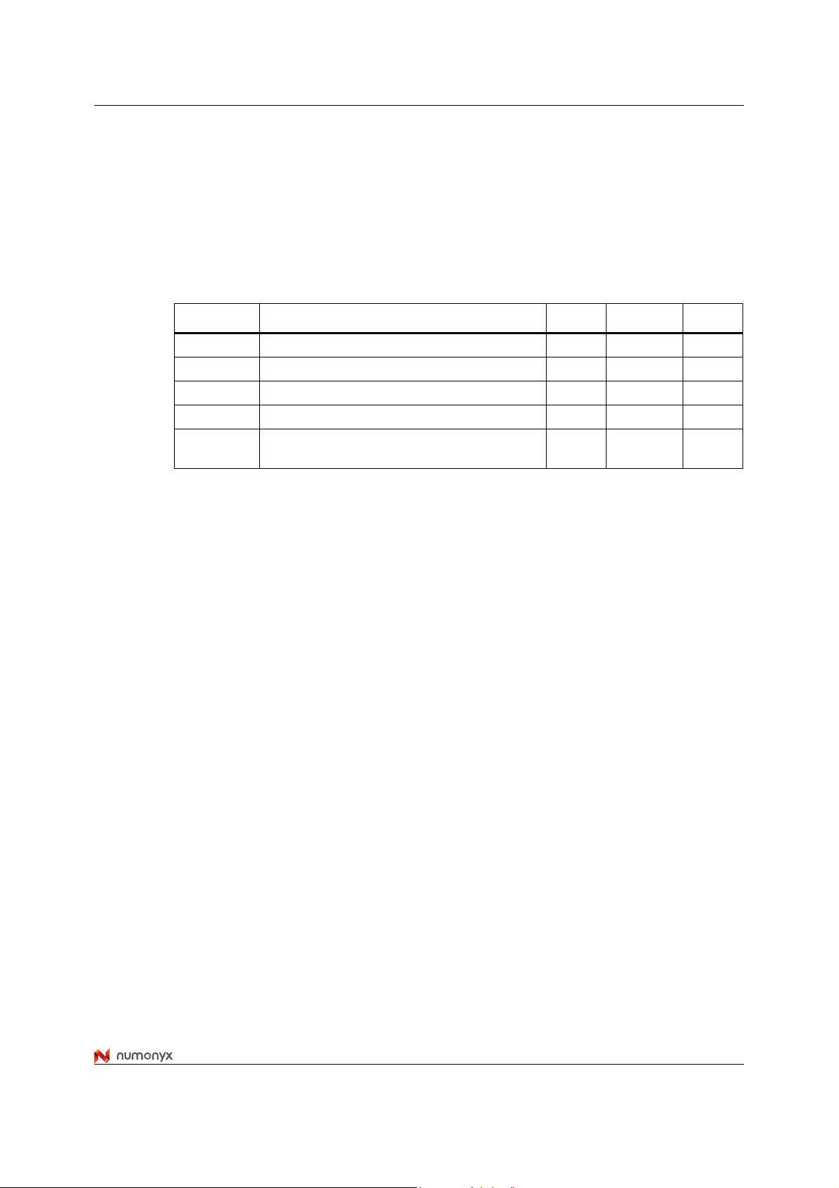
Figure 1. Logic diagram
V
CC
D
C
S
W
HOLD
Table 1. Signal names
Signal name Function Direction
C Serial Clock Input
D Serial Data input Input
Q Serial Data output Output
S
Write Protect Input
W
Hold Input
HOLD
Chip Select Input
M25P05-A
V
SS
Q
AI05757
V
CC
V
SS
6/52
Supply voltage Supply
Ground Supply
Page 7

M25P05-A Description
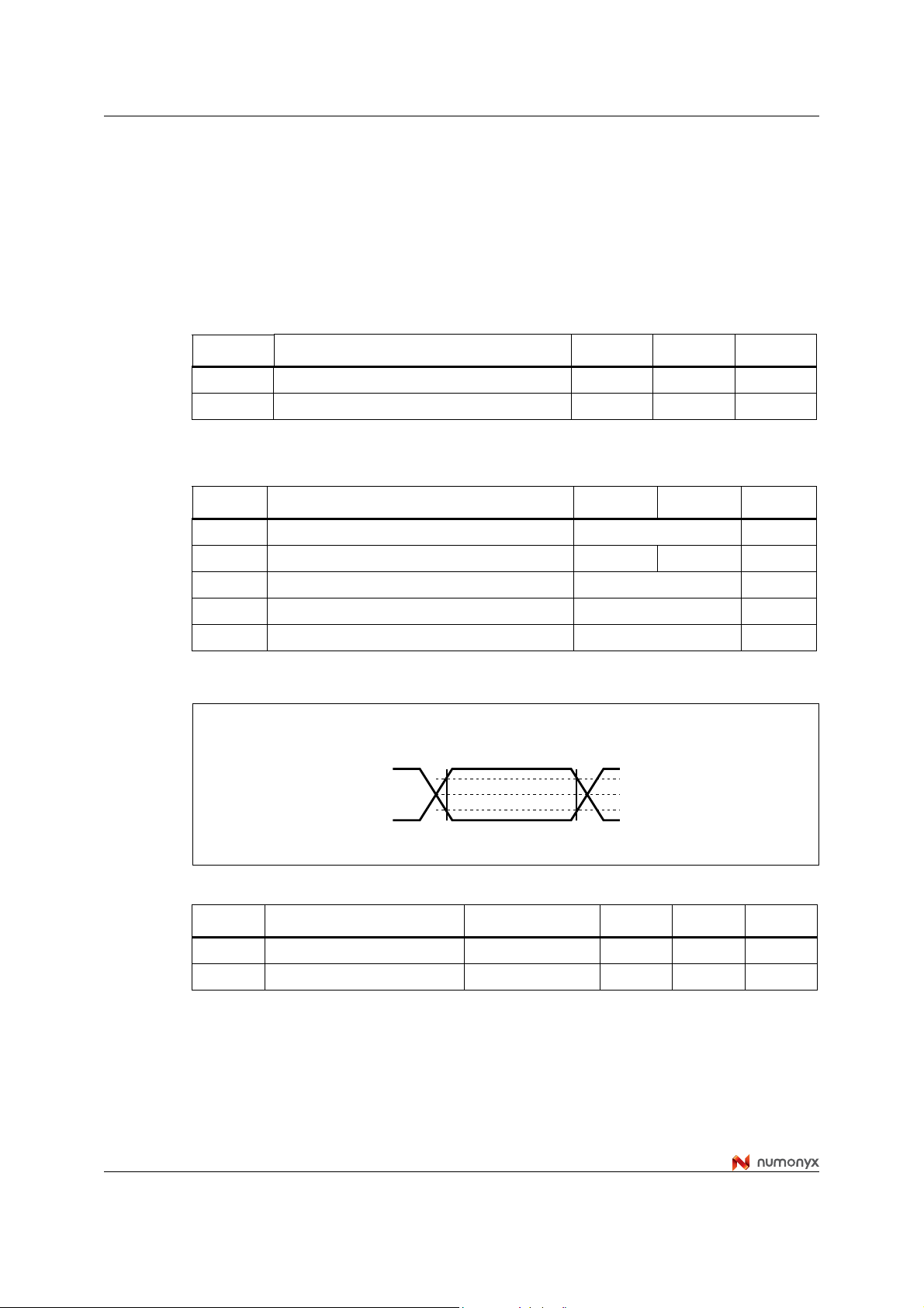
Figure 2. SO, VFQFPN and TSSOP connections
M25P05-A
SV
1
2
3
W
4
SS
1. There is an exposed central pad on the underside of the VFQFPN package. This is pulled, internally, to
VSS, and must not be allowed to be connected to any other voltage or signal line on the PCB.
2. See Package mechanical section for package dimensions, and how to identify pin-1.
8
7
6
5
AI05758B
CC
HOLDQ
C
DV
7/52
Page 8

Signal descriptions M25P05-A
2 Signal descriptions
2.1 Serial Data output (Q)
This output signal is used to transf er data serially out of the de vice . Data is shifted out on the
falling edge of Serial Clock (C).
2.2 Serial Data input (D)
This input signal is used to transfer data serially into the device. It receives instructions,
addresses, and the data to be programmed. Values are latched on the rising edge of Serial
Clock (C).
2.3 Serial Clock (C)
This input signal provides the timing of the serial interface. Instructions, addresses, or data
present at Serial Data input (D) are latched on the rising edge of Serial Clock (C). Data on
Serial Data output (Q) changes after the falling edge of Serial Clock (C).
2.4 Chip Select (S)
When this input signal is High, the device is deselected and Serial Data output (Q) is at high
impedance. Unless an internal program, erase or write status register cycle is in progress,
the device will be in the standby mode (this is not the deep power-do wn mode). Driving Chip
Select (S
After power-up, a falling edge on Chip Select (S
instruction.
) Low enables the device, placing it in the active power mode.
2.5 Hold (HOLD)
The Hold (HOLD) signal is used to pause any serial communications with the de vice without
deselecting the device.
During the Hold condition, the Serial Data output (Q) is high impedance, and Serial Data
input (D) and Serial Clock (C) are don’t care.
To start the Hold condition, the device must be selected, with Chip Select (S
2.6 Write Protect (W)
The main purpose of this input signal is to freeze the size of the area of mem ory that is
protected against program or erase instructions (as specified by the values in the BP1 and
BP0 bits of the status register).
) is required prior to the start of any
) driven Low.
8/52
Page 9

M25P05-A Signal descriptions
2.7 VCC supply voltage
VCC is the supply voltage.
2.8 VSS ground
VSS is the reference for the VCC supply voltage.
9/52
Page 10
SPI modes M25P05-A
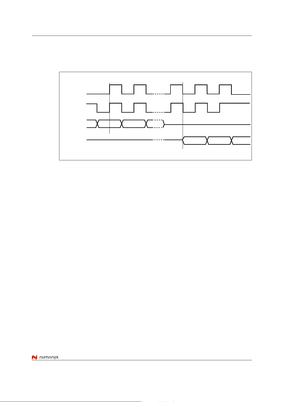
3 SPI modes
These devices can be drive n by a microcontroller with its SPI peripheral running in either of
the two following modes:
● CPOL=0, CPHA=0
● CPOL=1, CPHA=1
For these two modes, input data is latched in on the rising edge of Serial Clock (C), and
output data is available from the falling edge of Serial Clock (C).
The difference between the two modes, as shown in Figure 4, is the clock polarity when the
bus master is in standby mode and not transferring data:
● C remains at 0 for (CPOL=0, CPHA=0)
● C remains at 1 for (CPOL=1, CPHA=1)
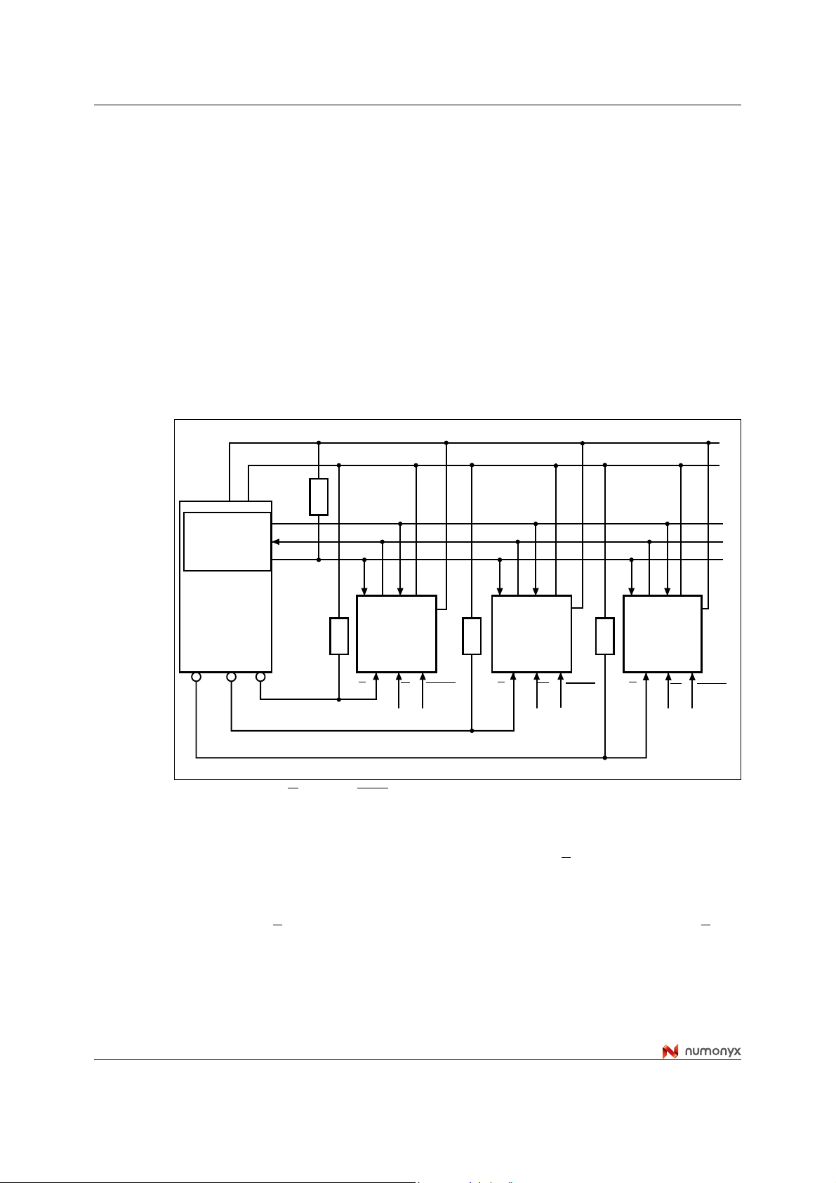
Figure 3. Bus master and memory devices on the SPI bus
V
SS
V
CC
R
SPI interface with
(CPOL, CPHA) =
(0, 0) or (1, 1)
SPI bus master
CS3 CS2 CS1
1. The Write Protect (W) and Hold (HOLD) signals should be driven, High or Low as appropriate.
SDO
SDI
SCK
device
W
V
CC
HOLD
V
CQD
RR R
SPI memory
S
CQD
SS
SPI memory
S
device
W
V
CC
HOLD
V
CQD
SS
SPI memory
device
S
V
CC
V
SS
HOLD
W
AI12836b
Figure 3 shows an example of three de vices connected to an MCU , on an SPI bus . Only one
device is selected at a time, so only one device drives the Serial Data output (Q) line at a
time, the other devices are high impedance. Resistors R (represented in Figure 3) ensure
that the M25P05-A is not selected if the bus master leav es th e S
line in the high impedance
state. As the bus master ma y enter a state where all inpu ts/outputs are in high impedance at
the same time (for example, when the bus master is reset), the clock line (C) must be
connected to an external pull-down resistor so that, when all inputs/outputs become high
impedance, the S
C do not become High at the same time, and so, that the t
typical value of R is 100 kΩ, assuming that the time constant R*C
line is pulled High while the C line is pulled Low (thus ensuring that S a nd
requirement is met). The
SHCH
(Cp = parasitic
p
capacitance of the bus line) is shorter than the time during which the bus master leaves the
SPI bus in high impedance.
10/52
Page 11
M25P05-A SPI modes
Example: Cp = 50 pF, that is R*Cp = 5 µs <=> the application must ensure that the bus
master never leaves the SPI bus in the high impedance state for a time period shorter than
5µs.
Figure 4. SPI modes supported
CPHA
CPOL
C
0
0
1
1
C
D
Q
MSB
MSB
AI01438B
11/52
Page 12

Operating features M25P05-A
4 Operating features
4.1 Page programming
To program one data byte, two in structions are required: Write Enable (WREN), which is one
byte, and a page program (PP) sequence, which consists of four bytes plus data. This is
followed by the internal program cycle (of duration t
To spread this overhead, the page program (PP) instruction allows up to 256 bytes to be
programmed at a time (changing bits from 1 to 0), provided that they lie in consecutive
addresses on the same page of memory.
For optimized timings, it is recommended to use the page program (PP) instruction to
program all consecutive targeted bytes in a single sequence versus using several page
program (PP) sequences with each containing only a few bytes (see Section 6.8: Page
program (PP) and Table 14: Instruction times).
4.2 Sector erase and bulk erase
The page program (PP) instruction allows bits to be reset from 1 to 0. Before this can be
applied, the bytes of memory need to have been erased to all 1s (FFh). This can be
achiev ed either a sector a t a time, using the sector erase (SE) inst ruction, or t hroug hout the
entire memory, using the bulk erase (BE) instruction. This starts an internal erase cycle (of
duration t
The erase instruction must be preceded by a write enable (WREN) instruction.
or tBE).
SE
PP
).
4.3 Polling during a write, program or erase cycle
A further improvement in the time to write status register (WRSR), program (PP) or erase
(SE or BE) can be achiev ed by not waiting for the w o rst case d elay (t
write in progress (WIP) bit is provided in the status register so that the application program
can monitor its value, polling it to establish when the previous write cycle, program cycle or
erase cycle is complete.
, tPP, tSE, or tBE). The
W
4.4 Active power, standby power and deep power-down modes
When Chip Select (S) is Low, the device is selected, and in the active power mode.
When Chip Select (S
mode until all internal cycles have completed (prog ram, erase, write status register). The
device then goes in to the standby power mode. The device consumption drops to I
The deep power-do wn mo de is en tere d when th e specific in struction (the de ep power-down
(DP) instruction) is executed. The device consumption drops further to I
remains in this mode until another specific instruction (the release from deep power-down
and read electronic signature (RES) instruction) is executed.
While in the deep power-down mode, the device ignores all write, program and erase
instructions (see Section 6.11: Deep power-down (DP)). This can be used as an extra
software protection mechanism, when the device is not in active use, to protect the device
from inadvertent write, program or erase instructions .
) is High, the device is dese lected, b ut could rema in in the activ e pow er
.
CC1
. The device
CC2
12/52
Page 13

M25P05-A Operating features
4.5 Status register
The status register contains a number of status and control bits, as shown in Table 6, that
can be read or set (as appropriate) by specific instructions.
4.5.1 WIP bit
The write in progress (WIP) bit indicates whether the memory is busy with a write status
register, program or erase cycle.
4.5.2 WEL bit
The write enable latch (WEL) bit indicates the status of the internal write enable latch.
4.5.3 BP1, BP0 bits
The block protect (BP1, BP0) bits are non-volatile. They define the size of the area to be
software protected against program and erase instructions.
4.5.4 SRWD bit
The status register write disable (SRWD) bit is operated in conjunction with the Write
Protect (W
allow the device t o be put in the hardwar e protected mode . In this mode, the non- volatile bits
of the status register (SRWD, BP1, BP0) become read-only bits.
) signal. The status register write disable ( SRWD) b it and Write Protect (W) signal
13/52
Page 14
Operating features M25P05-A
4.6 Protection modes
The environments where non-volatile memory devices are used can be very noisy. No SPI
device can operate correctly in the presence of excessive noise. To help combat this, the
M25P05-A features the following data protection mechanisms:
● Power on reset and an internal timer (t
changes while the power supply is outside the operating specification
● Program, er ase and write status reg ister instructions are chec ked that they consist of a
number of clock pulses that is a multiple of eight, before they are accepted for
execution
● All instructions that modify data must be preceded by a write enable (WREN)
instruction to set the write enable latch (WEL) bit. This bit is returned to its reset state
by the following events:
–Power-up
– Write disable (WRDI) instruction completion
– Write status register (WRSR) instruction completion
– Page program (PP) instruction completion
– Sector erase (SE) instruction completion
– Bulk erase (BE) instruction completion
● The block protect (BP1, BP0) bits allow part of the memory to be configured as read-
only. This is the software protected mode (SPM)
● The Write Protect (W) signal, in co-ope ration with the status register write disable
(SRWD) bit, allows the block protect (BP1, BP0) bits and status register write disable
(SRWD) bit to be write-protected. This is the hardware protected mode (HPM)
● In addition to the low power consumption feature, the deep power-down mode offers
extra software protection, as all write, program and erase instructions are ignored.
Table 2. Protected area sizes
) can provide protection against inadvertent
PUW
Status Register
content
BP1 bit BP0 bit Protected area Unprotected area
0 0 none All sectors (sectors 0 and 1)
0 1
1 0
1 1 All sectors (sectors 0 and 1) none
1. The device is ready to accept a bulk erase instruction if, and only if, both block protect (BP1, BP0) are 0.
14/52
No protection against page program (PP) and sector erase (SE)
All sectors (sectors 0 and 1) protected against bulk erase (BE)
Memory content
Page 15
M25P05-A Operating features
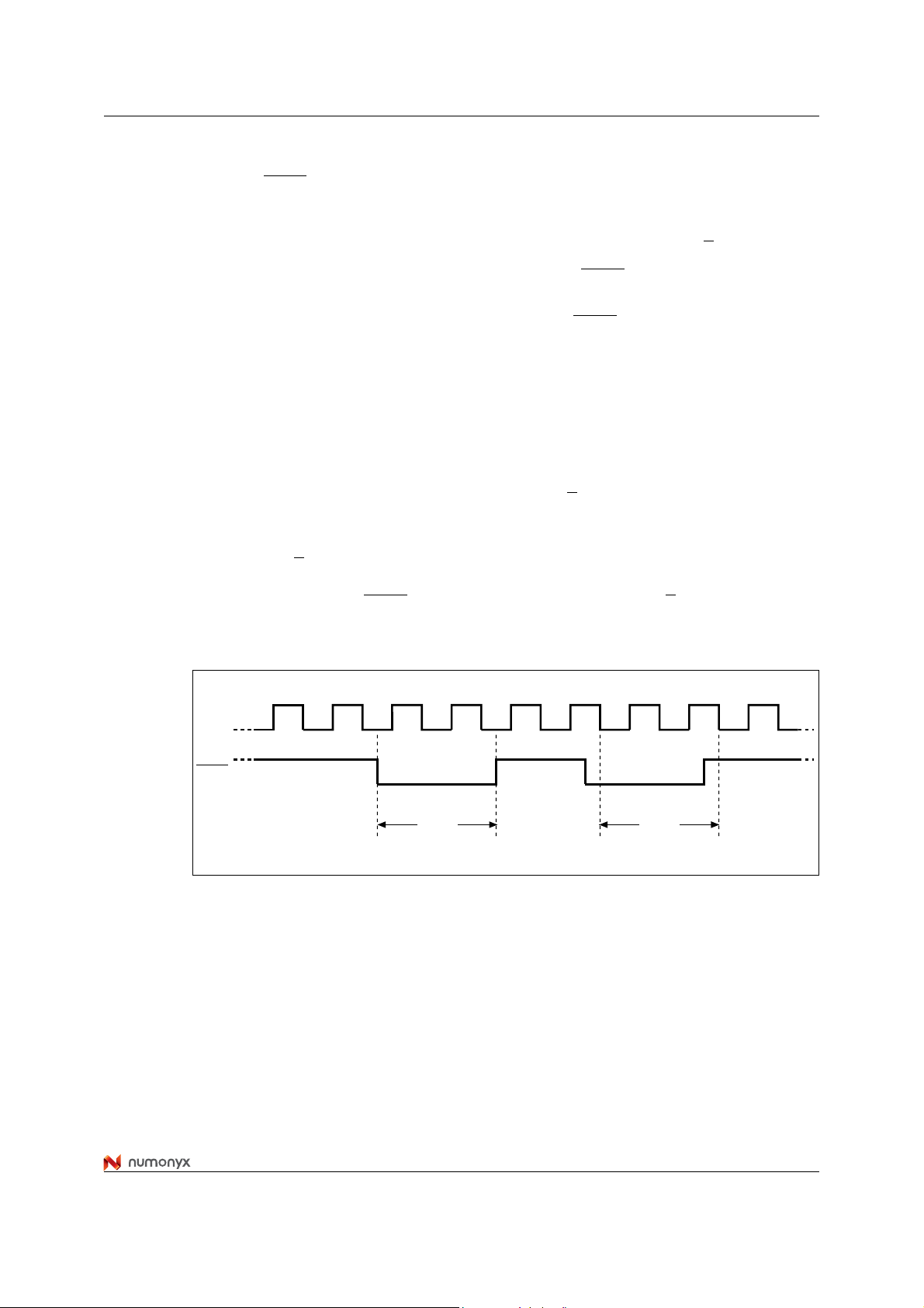
4.7 Hold condition
The Hold (HOLD) signal is used to pause any serial communications with the de vice without
resetting the clocking sequence. However, taking this signal Low does not terminate any
write status register, program or erase cycle that is currently in progress.
To enter the hold condition, the device must be selected, with Chip Select (S
The hold condition starts on the falling edge of the Hold (HOLD
) signal, provided that this
) Low.
coincides with Serial Clock (C) being Low (as shown in Figure 5).
The hold condition ends on the rising edge of the Hold (HOLD
) signal, provided that this
coincides with Serial Clock (C) being Low.
If the falling edge does not coincide with Serial Clock (C) being Low, the hold condition
starts after Serial Clock (C) next goes Low. Similarly , if the rising edge does not coincide
with Serial Clock (C) being Low, the hold condition ends after Serial Clock (C) next goes
Low (this is shown in Figure 5).
During the hold condition, the Serial Data output (Q) is high impedance, and Serial Data
input (D) and Serial Clock (C) are don’t care.
Normally , the de vice is k ept selected, with Chip Select (S
) driven Low, for the whole duration
of the hold condition. This is to ensure that the state of the inte rnal logic remains unchanged
from the moment of entering the hold condition.
If Chip Select (S
) goes High while the device is in the hold condition, this has the effect of
resetting the internal logic of the device. To restart communication with the device, it is
necessary to drive Hold (HOLD
) High, and then to drive Chip Select (S) Low. This prevents
the device from going back to the hold condition.
Figure 5. Hold condition activation
HOLD
C
Hold
condition
(standard use)
15/52
Hold
condition
(non-standard use)
AI02029D
Page 16
Memory organization M25P05-A
5 Memory organization
The memory is organized as:
● 65,536 b ytes (8 bits each)
● 2 sectors (256 Kbits, 32768 bytes each)
● 256 pages (256 bytes each).
Each page can be individually prog rammed ( bits are prog rammed from 1 t o 0). The de vice is
sector or bulk erasable (bits are erased from 0 to 1) but not page erasable.
Table 3. Memory organization
Sector Address range
1 08000h 0FFFFh
0 00000h 07FFFh
16/52
Page 17

M25P05-A Memory organization
Figure 6. Block diagram
HOLD
W
S
C
D
Q
Control logic
Address register
and counter
08000h
Y decoder
High voltage
generator
I/O shift register
256 byte
data buffer
Status
register
0FFFFh
Size of the
read-only
memory area
00000h
000FFh
256 bytes (page size)
X decoder
AI05759
17/52
Page 18

Instructions M25P05-A
6 Instructions
All instructions, addresses and data are shifted in and ou t of the device, most significant bit
first.
Serial Data input (D) is sampled on the first rising edge of Serial Clock (C) after Chip Select
(S
) is driven Low. Then, the one-byte instruction code must be shifte d in to t he device, most
significant bit first, on Serial Data input (D), each bit being latched on the rising edges of
Serial Clock (C).
The instruction set is listed in Table 4.
Every instruction sequence starts with a one-byte instruction code. Depending on the
instruction, this might be followed by address bytes, or by data bytes , or by both or none.
Chip Select (S
shifted in.
In the case of a read data bytes (READ), read d ata bytes at higher speed (Fast_Read), read
identification (RDID), read status register (RDSR) or release from deep power-down, and
read electronic signature (RES) instruction, the shifted-in instruction sequence is followed
by a data-out sequence. Chip Select (S
sequence is being shifted out.
) must be driven High after the last bit of the inst ruction sequence has been
) can be driven High after any bit of the data-out
In the case of a page program (PP), secto r erase (SE), b ulk er ase (BE) , write status register
(WRSR), write enable (WREN), write disable (WRDI) or deep power-down (DP) instruction,
Chip Select (S
rejected, and is not e xecuted. That is, Chip Select (S
clock pulses after Chip Select (S
All attempts to access the memory array during a write status register cycl e, program cycle
or erase cycle are ignored, and the internal write status register cycle, program cycle or
erase cycle continues unaff ected.
) must be driven High exactly at a byte boundary, otherwise the instruction is
) must driven High when t he n umber of
) being driven Low is an exact multiple of eight.
18/52
Page 19
M25P05-A Instructions
Table 4. Instruction set
Instruction Description
One-byte instruction
code
Address
bytes
Dummy
bytes
Data
bytes
WREN Write enable 0000 0110 06h 0 0 0
WRDI Write disable 0000 0100 04h 0 0 0
(1)
RDID
Read identification 1001 1111 9Fh 0 0 1 to 3
RDSR Read status register 0000 0101 05h 0 0 1 to ∞
WRSR Write status register 0000 0001 01h 0 0 1
READ Read data bytes 0000 0011 03h 3 0 1 to ∞
FAST_READ
Read data bytes at higher
speed
0000 1011 0Bh 3 1 1 to ∞
PP Page program 0000 0010 02h 3 0 1 to 256
SE Sector erase 1101 1000 D8h 3 0 0
BE Bulk erase 1100 0111 C7h 0 0 0
DP Deep power-down 1011 1001 B9h 0 0 0
Release from deep powerdown, and read electronic
RES
signature
1010 1011 ABh
Release from deep powerdown
1. The read identification (RDID) instruction is available only in products with process technology code X and
Y (see application note AN1995).
0 3 1 to ∞
0 0 0
6.1 Write enable (WREN)
The write enable (WREN) instruction (Figure 7) sets the write enable latch (WEL) bit.
The write enable latch (WEL) bit mu st be set p rior to e v ery page progra m (PP), sector er ase
(SE), bulk erase (BE) and write status register (WRSR) instruction.
The write enable (WREN) instruction is entered by driving Chip Select (S
instruction code, and then driving Chip Select (S
Figure 7. Write enable (WREN) instruction sequence
S
C
D
Q
0
21 34567
Instruction
High Impedance
) Low, sending the
) High.
AI02281E
19/52
Page 20

Instructions M25P05-A
6.2 Write disable (WRDI)
The write disable (WRDI) instruction (Figure 8) resets the write enable latch (WEL) bit.
The write disable (WRDI) instruction is entered by driving Chip Select (S
instruction code, and then driving Chip Select (S
) High.
The write enable latch (WEL) bit is reset under the following conditions:
● Power-up
● Write disable (WRDI) instruction completion
● Write status register (WRSR) instruction completion
● P age program (PP) instruction completion
● Sector erase (SE) instruction completion
● Bulk erase (BE) instruction completion.
Figure 8. Write disable (WRDI) instruction sequence
S
0
21 34567
C
Instruction
D
High Impedance
Q
AI03750D
) Low, sending the
20/52
Page 21
M25P05-A Instructions
6.3 Read identification (RDID)
The read identification (RDID) instruction is available in products with process technology
code X and Y.
The read identification (RDID) instruction allows the 8-bit manufacturer identification to be
read, followed by two bytes of device identification. The manufacturer identification is
assigned by JEDEC, and has the value 20h for Numonyx. The device identification is
assigned by the device manufacturer, and indicates the memory type in the first byte (20h),
and the memory capacity of the device in the second byte (10h).
Any read identification (RDID) instruction while an erase or program cycle is in progress, is
not decoded, and has no effect on the cycle that is in progress.
The read identification (RDID) instruction should not be issued while the device is in deep
power-down mode.
The device is first selected by driving Chip Select (S
) Low. Then, the 8-bit instruction code
for the instruction is shifted in. This is followed by the 24-bit device identification, stored in
the memory, being shifted out on Serial Data output (Q), each bit being shifted out during
the falling edge of Serial Clock (C).
The instruction sequence is shown in Figure 9.
The read identification (RDID) instruction is terminated by driving Chip Select (S
) High at
any time during data output.
When Chip Select (S
) is driven High, the device is put in the st andby power mode. Once in
the standby pow er mode , the device waits to be selected, so that it can receive, deco de and
execute instructions.
Table 5. Read identification (RDID) data-out sequence
Device identification
Manufacturer identification
Memory type Memory capacity
20h 20h 10h
Figure 9. Read identification (RDID) instruct ion sequence and data-out sequence
S
21 3456789101112131415
0
C
Instruction
D
16 17 18 28 29 30 31
Q
High Impedance
Manufacturer identification
MSB
21/52
Device identification
15 1413 3210
MSB
AI06809b
Page 22

Instructions M25P05-A
6.4 Read status register (RDSR)
The read status register (RDSR) instruction allows t he status re gister to be read. The status
register may be read at any time, even while a program, erase or write status register cycle
is in progress. When one of these cycles is in progress, it is recommended to check the
write in progress (WIP) bit before sending a new instruction to the device. It is also possible
to read the status register continuously, as shown in Figure 10.
Table 6. Status register format
b7 b0
SRWD 0 0 0 BP1 BP0 WEL WIP
Status register write protect
Block protect bits
Write enable latch bit
Write in progress bit
The status and control bits of the status register are as follows:
6.4.1 WIP bit
The write in progress (WIP) bit indicates whether the memory is busy with a write status
register, program or erase cycle. When set to ‘1’, such a cycle is in progress, when reset to
‘0’ no such cycle is in progress.
6.4.2 WEL bit
The write enable latch (WEL) bit indicates the status of the internal write enable latch. When
set to ‘1’ the internal write enable latch is set, when set to ‘0’ the internal write enable latch is
reset and no write status register, program or erase instruction is accepted.
6.4.3 BP1, BP0 bits
The block protect (BP1, BP0) bits are non-volatile. They define the size of the area to be
software protected against program and erase instructions. These bits are written with the
write status register (WRSR) instruction. When one or both of the block protect (BP1, BP0)
bits is set to ‘1’, the relevant memory area (as defined in Table 2) becomes protected
against page program (PP) and sector erase (SE) instructions. The bloc k protect (BP1,
BP0) bits can be written provided that the hardware protected mode has not been set. The
bulk erase (BE) instruction is executed if, and only if, both block protect (BP1, BP0) bits are
0.
6.4.4 SRWD bit
The status register write disable (SRWD) bit is operated in conjunction with the Write
Protect (W
) signal. The status register write disable ( SRWD) bit and write protect (W) signal
allow the device to be put in the hardware protected mode (when the status register write
disable (SRWD) bit is set to ‘1’, and write protect (W
volatile bits of the status register (SRWD, BP1, BP0) become read-only bits and the write
status register (WRSR) instruction is no longer accepted for execution.
22/52
) is driven Low). In this mode, the non-
Page 23
M25P05-A Instructions
Figure 10. Read status register (RDSR) instruction sequence and data-out sequence
S
21 3456789101112131415
0
C
Instruction
D
Q
High Impedance
Status register out
7 6543210
MSB
6.5 Write status register (WRSR)
The write status register (WRSR) instruction allows new values to be written to the status
register . Bef o re it can be accepted, a write enab le (WREN) instruction must previously have
been executed. After the write enable (WREN) instruction has been decoded and executed,
the device sets the write enable latch (WEL).
The write status register (WRSR) instruction is entered by driving Chip Select (S
followed by the instruction code and the data byte on Serial Data input (D).
The instruction sequence is shown in Figure 11.
The write status register (WRSR) instruction has no effect on b6, b5, b4, b1 and b0 of the
status register. b6, b5 and b4 are always read as 0.
Chip Select (S
If not, the write status register (WRSR) instruction is not executed. As soon as Chip Select
(S
) is driven High, the self-timed write status register cycle (whose duration is tW) is initiated.
While the write status register cycle is in progress, the status register may still be read to
check the va lue of t he write in prog ress (WIP) bit. The write in progr ess (WIP) bit is 1 du ring
the self-timed write status register cycle, and is 0 when it is completed. At some unspecified
time before the cycle is completed, the write enable latch (WEL) is reset.
) must be driven High after t he eighth bit of th e data b y te has bee n latched in .
Status register out
7 6543210
MSB
7
AI02031E
) Low,
The write status register (WRSR) instruction allows the user to change the values of the
block protect (BP1 , BP0) bits, to define the siz e of the area that is to be tr eated as read-only,
as defined in Table 2. The write status register (WRSR) instruction also allows the user to
set or reset the status register write disab le (SR WD) bit in accordance with the Write Protect
(W
) signal. The status register write disable (SRWD) bit and Write Protect (W) signal allow
the device to be put in the hardware protected mode (HPM). The write status register
(WRSR) instruction is not executed once the hardware protected mode (HPM) is entered.
The protection features of the device are summarized in Table 7.
When the status register write disable (SRWD) bit of the status register is 0 (its initial
delivery state), it is possible to write to the status register provided that the write enable latch
(WEL) bit has previously been set by a write enable (WREN) instruction, regardless of the
whether Write Protect (W
) is driven High or Low.
23/52
Page 24
Instructions M25P05-A
When the status register write disable (SRWD) bit of the status register is set to ‘1’, two
cases need to be considered, depending on the state of Write Protect (W
● If Write Protect (W) is driven High, it is possible to write to the status register provided
):
that the write enable latch (WEL) bit has pre viously b een set b y a write enable (WREN)
instruction
● If Write Protect (W) is driven Low, it is not possible to write to the status register even if
the write enable latch (WEL) bit has previously been set by a write enable (WREN)
instruction (attempts to write to the status register are rejected, and are not accepted
for execution). As a consequence, all the data bytes in the memory area that are
software protected (SPM) b y the b lock protect (BP1, BP0) bit s of the status regist er , are
also hardware protected against data modification.
Regardless of the order of the two events, the hardware protected mode (HPM) can be
entered:
● by setting the status register write disable (SRWD) bit after driving Write Protect (W)
Low
● or by driving Write Protect (W) Low after setting the status register write disable
(SRWD) bit.
The only way to exit the hardware protected mode (HPM) once entered is to pull Write
Protect (W
) High.
If Write Protect (W
) is permanently tied High, the hardware protected mode (HPM) can
never be activated, and only the software protected mode (SPM), using the block protect
(BP1, BP0) bits of the status register, can be used.
Figure 11. Write status register (WRSR) instruction sequence
S
21 3456789101112131415
0
C
Instruction Status
D
High Impedance
Q
765432 0
MSB
register in
1
AI02282D
24/52
Page 25

M25P05-A Instructions
Table 7. Protection modes
Memory content
W
signal
SRWD
bit
Mode
Write protection of the status
register
Protected
(1)
area
Unprotected
area
(1)
10
00
11
Software
protected
(SPM)
Hardware
01
protected
(HPM)
1. As defined by the values in the block protect (BP1, BP0) bits of the status register, as shown in Table 2.
Status register is writable (if the
WREN instruction has set the WEL
bit).
The values in the SRWD, BP1 and
BP0 bits can be changed
Status register is hardware write
protected.
The values in the SRWD BP1 and
BP0 bits cannot be changed
Protected
against page
program, sector
erase and bulk
erase
Protected
against page
program, sector
erase and bulk
erase
Ready to
accept page
program and
sector erase
instructions
Ready to
accept page
program and
sector erase
instructions
25/52
Page 26

Instructions M25P05-A
6.6 Read data bytes (READ)
The device is first selected by driving Chip Select (S) Low. The instruction code for the read
data bytes (READ) instruction is followed by a 3-byte address (A23-A0), each bit being
latched-in during the rising edge of Serial Clock (C). Then the memory contents, at that
address, is shifted out on Serial Data output (Q), each bit being shifted out, at a maximum
frequency f
The instruction sequence is shown in Figure 12.
The first byte addressed can be at any location. The address is automatically incremented
to the next higher address after each byte of data is shifted out. The whole memory can,
therefore, be read with a single read data bytes (READ) instruction.
There is no address roll-over; when the highest address (0FFFFh) is reached, the
instruction should be terminated.
, during the falling edge of Serial Clock (C).
R
The read data bytes (READ) instruction is terminated by driving Chip Select (S
Select (S
) can be driven High at any time during data output. Any read data bytes (READ)
) High. Chip
instruction, while an erase, program or write cycle is in progress, is rejected without having
any effects on the cycle that is in progress.
Figure 12. Read data bytes (READ) instruction sequence and data-out sequence
S
21 345678910 2829303132333435
0
C
Instruction 24-bit address
23
D
High Impedance
Q
1. Address bits A23 to A16 must be set to 00h.
2221 3210
MSB
76543 1 7
MSB
36 37 38
Data out 1
39
Data out 2
2
0
AI03748D
26/52
Page 27

M25P05-A Instructions
6.7 Read data bytes at higher speed (FAST_READ)
The device is first selected by driving Chip Select (S) Low. The instruction code for the read
data bytes at higher speed (FAST_READ) instruction is followed by a 3-byte address (A23A0) and a dummy byte, each bit being latched-in during the rising edge of Serial Clock (C).
Then the memory contents, at that address , is shifted out on Serial Data output (Q), each bit
being shifted out, at a maximum frequency f
The instruction sequence is shown in Figure 13.
The first byte addressed can be at any location. The address is automatically incremented
to the next higher address after each byte of data is shifted out. The whole memory can,
therefore, be read with a single read data bytes at higher spee d (FAST_READ) instruction.
There is no address roll-over; when the highest address (0FFFFh) is reached, the
instruction should be terminated.
The read data bytes at higher speed (FAST_READ) instruction is terminated by driving Chip
Select (S
) High. Chip Select (S) can be driven High at an y time during data output. An y r ead
data bytes at higher speed (F AST_READ) instruction, while an erase, program or write cycle
is in progress, is rejected without having any effects on the cycle that is in progr ess.
Figure 13. Read data bytes at higher speed (FAST_READ) instruction sequence
and data-out sequence
, during the falling edge of Serial Clock (C).
C
S
21 345678910 28293031
0
C
Instruction 24-bit address
23
D
High Impedance
Q
S
32 33 34 36 37 38 39 40 41 42 43 44 45 46
C
D
Q
765432 0
35
Dummy byte
2221 3210
1
DATA OUT 1
765432 0
MSB
47
DATA OUT 2
7 6543210
1
MSB MSB
7
1. Address bits A23 to A16 must be set to 00h.
AI04006
27/52
Page 28

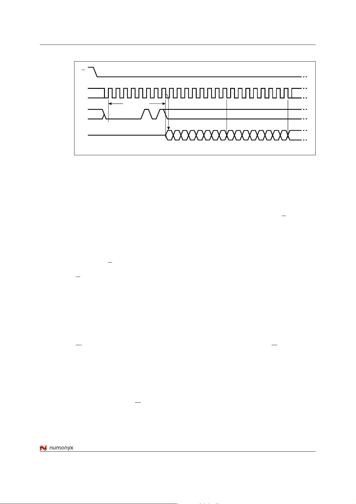
Instructions M25P05-A
6.8 Page program (PP)
The page program (PP) instruction allo ws bytes to b e programmed in t he memory (changing
bits from 1 to 0). Before it can be acce pted, a write enable (WREN) instruction must
previously have been executed. After the write enable (WREN) instruction has been
decoded, the device sets the write enable latch (WEL).
The page program (PP) instruction is entered b y driving Chip Select (S
instruction code, three address bytes and at least one data byte on Serial Data input (D). If
the 8 least significant address bits (A7-A0) are not all zero, all transmitted data that goes
beyond the end of t he current page are programmed from the start address of the same
page (from the address whose 8 least significant bits (A7-A0) are all zero). Chip Select (S
must be driven Low for the entire duration of the sequence.
The instruction sequence is shown in Figure 14.
If more than 256 by tes ar e se nt t o the device, previously latched data are discarded and the
last 256 data bytes are guaranteed t o be progr ammed correctly within the same page . If less
than 256 data bytes are sent to device, they are correctly programmed at the requested
addresses without having any effects on the other bytes of the same page.
For optimized timings, it is recommended to use the page program (PP) instruction to
program all consecutive targeted bytes in a single sequence versus using several page
program (PP) sequences with each containing only a few bytes (see Table 14: Instruction
times).
Chip Select (S
latched in, otherwise the page progr am (PP) instruction is not executed.
As soon as Chip Select (S
duration is t
may be read to check th e value of the write in progress (WIP) bit. The write in progress
(WIP) bit is 1 during the self-timed page program cycle, and is 0 when it is completed. At
some unspecified time before the cycle is completed, the write enable latch (WEL) bit is
reset.
) must be driven High after the eighth bit of the last data byte has been
) is driven High, the self-timed page program cycle (whose
) is initiated. While the page program cycle is in progress, the status register
PP
) Low, f ollowed b y the
)
A page program (PP) instruction applied to a page which is protected by the bloc k protect
(BP1, BP0) bits (see Table 3. and Table 2.) is not executed.
28/52
Page 29

M25P05-A Instructions
Figure 14. Page program (PP) instruction sequence
S
21 345678910 2829303132333435
0
C
Instruction 24-bit address
D
S
4241 43 44 45 46 47 48 49 50 52 53 54 5540
C
Data byte 2
D
765432 0
MSB MSB MSB
765432 0
1
1. Address bits A23 to A16 must be set to 00h.
23
2221 3210
MSB
51
Data byte 3 Data byte 256
1
765432 0
MSB
2073
2072
765432 0
36 37 38
Data byte 1
2075
2074
2076
1
2077
1
39
2079
2078
AI04082B
29/52
Page 30

Instructions M25P05-A
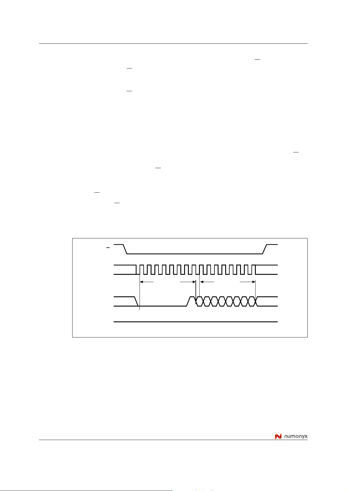
6.9 Sector erase (SE)
The sector erase (SE) instruction sets to ‘1’ (FFh) all bits inside the chosen sector. Before it
can be accepted, a write enable (WREN) instruction must previously have been executed.
After the write enable (WREN) instruction has been decoded, the device sets the write
enable latch (WEL).
The sector erase (SE) instruction is entered by driving Chip Select (S
) Low, followed by the
instruction code, and three address bytes on Serial Data input (D). Any address inside the
sector (see Table 3) is a valid address f or the sector erase (SE) instruction. Chip Select (S
must be driven Low for the entire duration of the sequence.
The instruction sequence is shown in Figure 15.
Chip Select (S
) must be driven High after the eighth bit of the last address byte has been
latched in, otherwise the sector erase (SE) instruction is not executed. As soon as Ch ip
Select (S
) is driven High, the self-timed sector erase cycle (whose duration is tSE) is
initiated. While the sector erase cycle is in progress, the status register may be read to
check the va lue of t he write in prog ress (WIP) bit. The write in progr ess (WIP) bit is 1 du ring
the self-timed sector erase cycle, and is 0 when it is completed. At some unspecified time
before the cycle is completed, the write enable latch (WEL) bit is reset.
A sector erase (SE) instruction applied to a page which is protected by the block protect
(BP1, BP0) bits (see Table 3 and Table 2) is not executed.
Figure 15. Sector erase (SE) instruction sequence
S
21 3456789 293031
0
C
Instruction
24-bit address
)
D
1. Address bits A23 to A16 must be set to 00h.
30/52
23 22 2 0
MSB
1
AI03751D
Page 31

M25P05-A Instructions
6.10 Bulk erase (BE)
The bulk erase (BE) instruction sets all bits to ‘1’ (FFh). Before it can be accepted, a write
enable (WREN) instruction must previously have been executed. After the write enable
(WREN) instruction has been decoded, the device sets the write enable latch (WEL).
The bulk erase (BE) instruction is entered by driving Chip Select (S
instruction code on Serial Data input (D). Chip Select (S
) must be driven Low for the entire
) Low, followed by the
duration of the sequence.
The instruction sequence is shown in Figure 16.
Chip Select (S
) must be driven High after the eighth bit of the instruction code has been
latched in, otherwise the bulk erase instruction is not executed. As soon as Chip Select (S
is driven High, the self-timed bulk erase cycle (whose duration is t
) is initiated. While the
BE
bulk erase cycle is in progress, the status register may be read to check the value of the
write in progress (WIP) bit. The write in progress (WIP) bit is 1 during the self-timed bulk
erase cycle, and is 0 when it is completed. At some unspecified time before the cycle is
completed, the write enable latch (WEL) bit is reset.
The bulk erase (BE) instruction is executed only if both block protect (BP1, BP0) bits are 0.
The bulk erase (BE) instruction is ignored if one, or more, sectors are protected.
Figure 16. Bulk erase (BE) instruction sequence
S
21 345670
C
Instruction
D
)
AI03752D
31/52
Page 32
Instructions M25P05-A
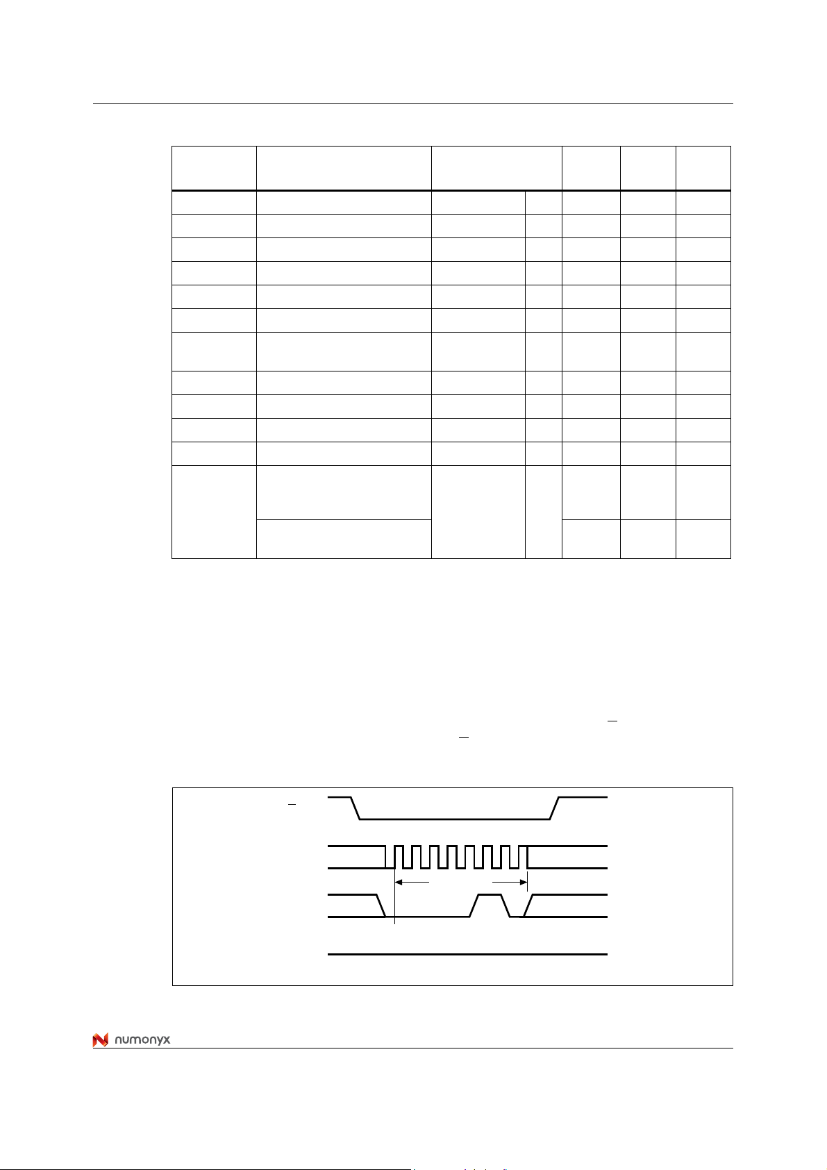
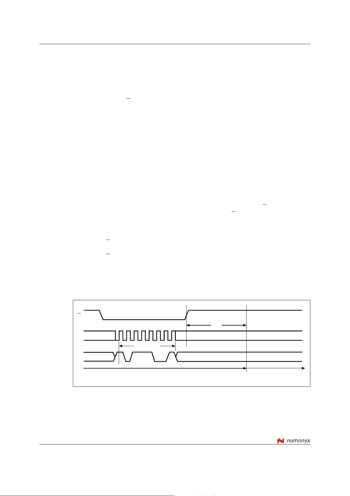
6.11 Deep power-down (DP)
Executing the deep power-down (DP) instruction is the only way to put the device in the
lowest consumption mode (the deep power-down mode). It can also be used as a software
protection mechanism, while the device is not in active use, as in this mode, the device
ignores all write, program and erase instructions.
Driving Chip Select (S
) High deselects the device, and puts the device in standby mode (if
there is no internal cycle currently in progress). But this mode is not the deep power-down
mode. The deep pow er-do wn mode can only be ente red b y e x ecut ing the deep po wer-do wn
(DP) instruction, subsequently reducing the standb y current (from I
CC1
to I
, as specified
CC2
in Table 13).
To take the device out of deep power-down mode, the release from deep power-down and
read electronic signature (RES) instruction must be issued. No other instruction must be
issued while the device is in deep power-down mode.
The release from deep pow er-down and read electron ic signature (RES) instruction, a nd the
read identification (RDID) instruction also allow t he electronic signature of the device to be
output on Serial Data output (Q).
The deep power-down mode automatically stops at power-down, and the device always
powers-up in the stan dby mode.
The deep power-down (DP) instruction is entered by driving Chip Select (S
by the instruction code on Serial Data input (D). Chip Select (S
) must be driven Low for the
) Low, followed
entire duration of the sequ ence.
The instruction sequence is shown in Figure 17.
Chip Select (S
) must be driven High after the eighth bit of the instruction code has been
latched in, otherwise the deep power-down (DP) instruction is not executed. As soon as
Chip Select (S
to I
and the deep power-down mode is entered.
CC2
) is driven High, it requires a delay of tDP before the supply cu rrent is r educe d
Any deep power-down (DP) instruction, while an erase, program or write cycle is in
progress, is rejected without having any effects on the cycle that is in progress.
Figure 17. Deep power-down (DP) instruction sequence
S
21 345670
C
Instruction
D
32/52
t
DP
Standby mode
Deep power-down mode
AI03753D
Page 33

M25P05-A Instructions
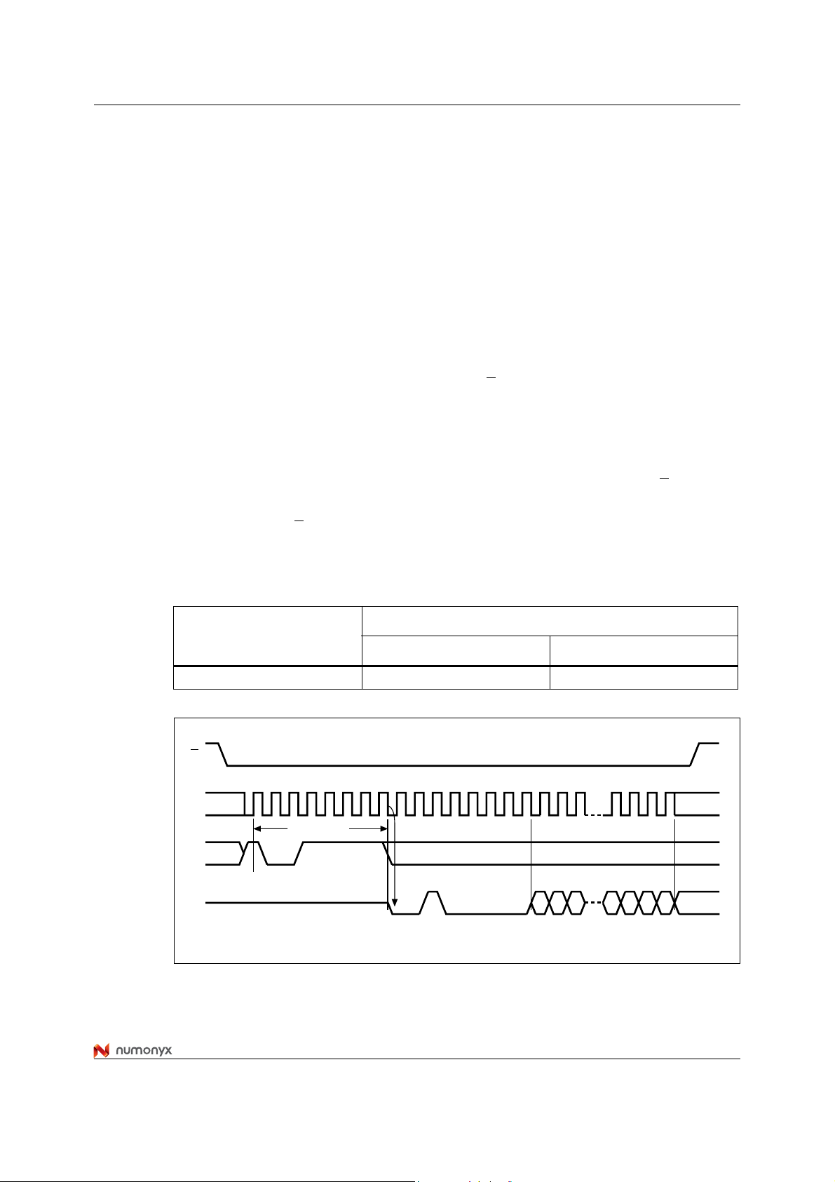
6.12 Release from deep power-down and read electronic signature (RES)
To take the device out of deep power-down mode, the release from deep power-down and
read electronic signature (RES) instruction must be issued. No other instruction must be
issued while the device is in deep power-down mode.
The instruction can also be used to read, on Serial Data output (Q), the 8-bit electronic
signature, whose value for the M25P05-A is 05h.
Except while an erase, program or write status register cycle is in pro gress , the release from
deep power-down and read electronic signature (RES) instruction always provides access
to the 8-bit electronic signature of the device, and can be applied even if the deep powerdown mode has not been entered.
Any release from deep pow er-down and re ad electronic signature (RES) instruction while an
erase, program or write status register cycle is in progress, is not decoded, and has no
effect on the cycle that is in progress.
The device is first selected by driving Chip Select (S
) Low. The instruction code is followed
by 3 dummy bytes, each bit being latched-in on Serial Data input (D) during the rising edge
of Serial Clock (C). Then, the 8-bit electronic signature, stored in the memory, is shifted out
on Serial Data output (Q), each bit being shifted out during the falling edge of Serial Clock
(C).
The instruction sequence is shown in Figure 18.
The release from deep power-down and read electronic signature (RES) instruction is
terminated by driving Chip Select (S
least once. Sending additional clock cycles on Serial Clock (C), while Chip Select (S
) High after the electronic signature has been read at
) is
driven Low, cause the electronic signature to be output repeatedly.
When Chip Select (S
) is driven High, the device is put in the standby power mode. If the
device was not pre viously in t he deep power- down mode , the transition to the st andby po wer
mode is immediate. If the de vice w as previously in the deep power-down mode, though, the
transition to the standby power mode is delayed by t
High for at least t
(max), as specified in Table 15. Once in the standby po wer mode, the
RES2
, and Chip Select (S) must remain
RES2
device waits to be selected, so that it can receive, decode and execute instructions.
Driving Chip Select (S
) High after the 8-bit instruction byte has been r eceiv ed b y t he de vice ,
but before the whole of the 8-bit electronic signature has been transmitted for the first time
(as shown in Figure 19), still ensures that the device is put into standby power mode. If the
device was not pre viously in t he deep power- down mode , the transition to the st andby po wer
mode is immediate. If the de vice w as previously in the deep power-down mode, though, the
transition to the standby power mode is delayed by t
High for at least t
(max), as specified in Table 15. Once in the standby po wer mode, the
RES1
, and Chip Select (S) must remain
RES1
device waits to be selected, so that it can receive, decode and execute instructions.
33/52
Page 34

Instructions M25P05-A
Figure 18. Release from deep power-down and read electronic signature (RES)
instruction sequence and data-out sequence
S
21 345678910 2829303132333435
0
C
Instruction 3 dummy bytes
23
D
High Impedance
Q
2221 3210
MSB
Electronic signature Out
765432 0
MSB
Deep power-down mode
36 37 38
1
1. The value of the 8-bit electronic signature, for the M25P05-A, is 05h.
Figure 19. Release from deep power-down (RES) instruction sequence
S
t
21 345670
C
Instruction
RES1
t
RES2
Standby mode
AI04047C
D
High Impedance
Q
34/52
Deep power-down mode
Standby mode
AI04078B
Page 35

M25P05-A Power-up and power-down
7 Power-up and power-down
At power-up and po w er- down, the device must not be se lected ( that is Chip Select ( S ) m ust
follow the voltage applied on V
● V
●
(min) at power-up, and then for a further delay of t
CC
VSS at power-down
A safe configuration is provided in Section 3: SPI modes.
To avoid data corruption and inadvertent write operations during power-up, a power on reset
(POR) circuit is included. The logic inside the device is held reset while V
power on reset (POR) threshold voltage, V
does not respond to any instruction.
Moreover, the device ignores all write enable (WREN), page program (PP), sector erase
(SE), bulk erase (BE) and write status register (WRSR) instructions until a time de lay of
t
has elapsed after the moment that VCC rises above the VWI threshold. However, the
PUW
correct operation of the de vice is not guar a nteed if, by this time, V
No write status register, p rogram or erase instructions should be sent until the later of:
● t
● t
after VCC passed the VWI threshold
PUW
after VCC passed the VCC(min) level
VSL
These values are specified in Table 8.
) until VCC reaches the correct value:
CC
VSL
– all operations are disabled, and the device
WI
is less than the
CC
is still below VCC(min).
CC
If the delay, t
selected for read instructions even if the t
, has elapsed, after VCC has risen above VCC(min), the device can be
VSL
delay is not yet fully elapsed.
PUW
At power-up, the device is in the following state:
● The device is in the standby mode (not the deep po wer-down mode)
● The write enable latch (WEL) bit is reset
● The write in progress (WIP) bit is reset.
Normal precautions must be taken for supply rail decoupling, to stabilize the V
Each device in a system should ha v e the V
rail decoupled by a suitable capacito r close to
CC
supply.
CC
the package pins (generally, this capacitor is of the order of 100 nF).
At power-down, when V
(POR) threshold voltage, V
drops from the operating voltage, to below the power on reset
CC
, all operations are disabled and the device does not respond
WI
to any instruction (the designer needs to be aw are that if a power- down occurs while a write,
program or erase cycle is in progress, some data corruption can result).
35/52
Page 36
Initial delivery state M25P05-A
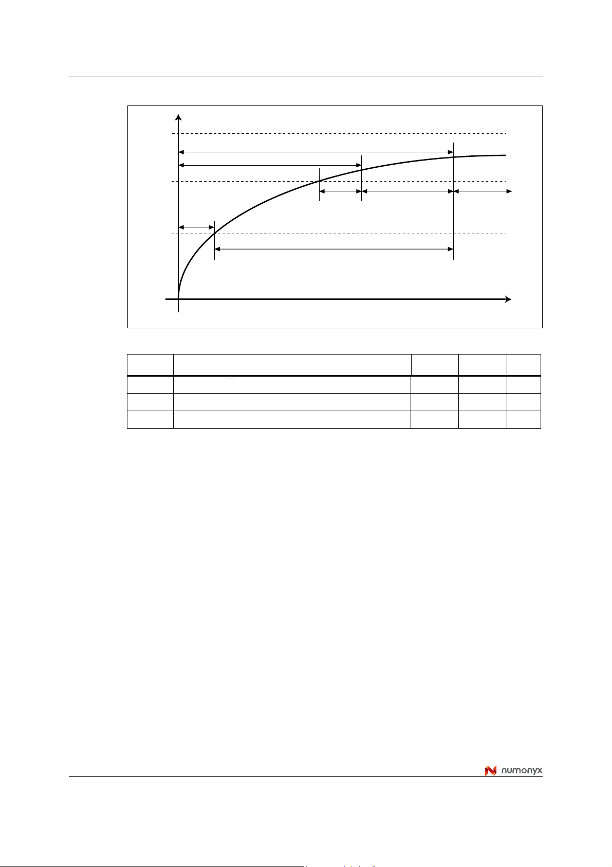
Figure 20. Power-up timing
V
CC
VCC(max)
Program, erase and write commands are rejected by the device
Chip selection not allowed
VCC(min)
Reset state
of the
device
V
WI
Table 8. Power-up timing and V
Symbol Parameter Min Max Unit
(1)
t
VSL
t
PUW
V
WI
1. These parameters are characterized only.
VCC(min) to S low 10 µs
(1)
Time delay to Write instruction 1 10 ms
(1)
Write inhibit voltage 1 2 V
8 Initial delivery state
threshold
WI
tVSL
tPUW
Read access allowed Device fully
accessible
time
AI04009C
The device is deliv ered with the memory array erased: all bits are set to ‘1’ (each byte
contains FFh). The status register contains 00h (all status register bits are 0).
36/52
Page 37
M25P05-A Maximum ratings
9 Maximum ratings
Stressing the device above the rating listed in Table 9: Absolute maximum ratings may
cause permanent damage to the device. These are stress ratings only and operation of the
device at these or any other conditions above those indicated in th e operating sections of
this specification is not implied. Exposure to absolute maximum rating conditions for
extended periods may aff ect device reliability.
Table 9. Absolute maximum ratings
Symbol Parameter Min Max Unit
T
STG
T
LEAD
V
IO
V
CC
V
ESD
1. Compliant with JEDEC Std J-STD-020C (for small body, Sn-Pb or Pb assembly), the Numonyx
ECOPACK® 7191395 specification, and the European directive on Restrictions on Hazardous Substances
(RoHS) 2002/95/EU.
2. JEDEC Std JESD22-A114A (C1 = 100 pF, R1 = 1500 Ω, R2 = 500 Ω).
Storage temperature –65 150 °C
Lead temperature during soldering see
(1)
Input and output voltage (with respect to ground) –0.6 VCC+0.6 V
Supply voltage –0.6 4.0 V
Electrostatic discharge voltage (human body
(2)
model)
–2000 2000 V
°C
37/52
Page 38
DC and AC parameters M25P05-A
10 DC and AC parameters
This section summarizes the operating and measurement conditions, and the DC and AC
characteristics of the device. The parameters in the DC and AC characteristic tables that
follow are derived from tests performed under the measurement conditions summarized in
the relevant tables. Designers should check that the operating conditions in their circuit
match the measurement conditions when relying on the quoted parameters.
Table 10. Operating conditions
Symbol Parameter Min Max Unit
V
CC
T
1. Only in products with process technology code Y. In products with process technology code X, VCC(min) is
2.7 V.
Table 11. AC measurement conditions
Supply voltage 2.3
Ambient operating temperature –40 85 °C
A
(1)
Symbol Parameter Min Max Unit
(1)
3.6 V
C
Load capacitance 30 pF
L
Input rise and fall times 5 ns
Input pulse voltages 0.2VCC to 0.8V
Input timing reference voltages 0.3V
Output timing reference voltages V
1. Output Hi-Z is defined as the point where data out is no longer driven.
to 0.7V
CC
CC
CC
CC
/ 2 V
Figure 21. AC measurement I/O wavef orm
Input levels
0.8V
CC
0.2V
CC
Table 12. Capacitance
(1)
Symbol Parameter Test condition Min Max Unit
C
OUT
C
1. Sampled only, not 100% tested, at T
Output capacitance (Q) V
Input capacitance (other pins) VIN = 0 V 6 pF
IN
= 25 °C and a frequency of 25 MHz.
A
= 0 V 8 pF
OUT
Input and output
timing reference levels
0.7V
0.5V
0.3V
AI07455
CC
CC
CC
V
V
38/52
Page 39

M25P05-A DC and AC parameters
Table 13. DC characteristics
Symbol Parameter
I
Input leakage current ± 2 µA
LI
Output leakage current ± 2 µA
I
LO
I
I
I
I
I
I
I
V
V
Table 14. Instruction times
Standby current S = VCC, V
CC1
Deep power-down current S = VCC, V
CC2
Operating current (READ)
CC3
Operating current (PP) S = V
CC4
Operating current (WRSR) S = V
CC5
Operating current (SE) S = V
CC6
Operating current (BE) S = V
CC7
Input low voltage – 0.5 0.3V
V
IL
V
Input high voltage 0.7V
IH
Output low voltage IOL = 1.6 mA 0.4 V
OL
Output high voltage IOH = –100 µAV
OH
Test condition (in addition to
those in Table 10.)
= VSS or V
C = 0.1V
IN
= VSS or V
IN
/ 0.9.VCC at 50 MHz,
CC
CC
CC
Q = open
C = 0.1V
/ 0.9.VCC at 25 MHz,
CC
Q = open
CC
CC
CC
CC
Min Max Unit
50 µA
5µA
8mA
4mA
15 mA
15 mA
15 mA
15 mA
CC
CCVCC
–0.2 V
CC
+0.4 V
V
Test conditions specified in Table 10 and Table 11.
Symbol Alt. Parameter Min Typ Max Unit
t
W
(1)
t
PP
t
SE
t
BE
1. When using the page program (PP) instruction to program consecutive bytes, optimized timings are
obtained with one sequence including all the bytes versus several sequences of only a few bytes (1 ≤ n ≤
256).
2. tPP=2µs+8µs*[int(n-1)/2+1]+4µs*[int(n-1)/2]+2µs, only in products with process technology code X and Y.
Write status register cycle time 5 15 ms
Page program cycle time (256 bytes) 1.4
Page program cycle time (n bytes) 0.4+n*1/256
(2)
5ms
Sector erase cycle time 0.65 3 s
Bulk erase cycle time 0.85 6 s
39/52
Page 40
DC and AC parameters M25P05-A
Table 15. AC characteristics (25 MHz operation)
Test conditions specified in Table 10 and Table 11.
Symbol Alt. Parameter Min Typ Max Unit
Clock frequency for the following instructions:
f
C
f
F AS T_READ, PP, SE, BE, DP, RES, WREN, WRDI,
C
RDSR, WRSR
D.C. 25 MHz
f
R
(1)
t
CH
(1)
t
CL
(2)
t
CLCH
(2)
t
CHCL
t
SLCHtCSS
t
CHSL
t
DVCHtDSU
t
CHDXtDH
t
CHSH
t
SHCH
t
SHSLtCSH
(2)
t
SHQZ
t
CLQV
t
CLQXtHO
t
HLCH
t
CHHH
t
HHCH
t
CHHL
(2)
t
HHQX
(2)
t
HLQZ
(4)
t
WHSL
(4)
t
SHWL
(2)
t
DP
(2)
t
RES1
Clock frequency for read instructions D.C. 20 MHz
t
Clock high time 18 ns
CLH
t
Clock low time 18 ns
CLL
Clock rise time
Clock fall time
(3)
(peak to peak)
(3)
(peak to peak) 0.1 V/ns
0.1 V/ns
S active setup time (relative to C) 10 ns
S not active hold time (relative to C) 10 ns
Data in setup time 5 ns
Data in hold time 5 ns
S active hold time (relative to C) 10 ns
S not active setup time (relative to C) 10 ns
S deselect time 100 ns
t
Output disable time 15 ns
DIS
tVClock Low to Output Valid 15 ns
Output hold time 0 ns
HOLD setup time (relative to C) 10 ns
HOLD hold time (relative to C) 10 ns
HOLD setup time (relative to C) 10 ns
HOLD hold time (relative to C) 10 ns
tLZHOLD to Output Low-Z 15 ns
t
HOLD to Output High-Z 20 ns
HZ
Write protect setup time 20 ns
Write protect hold time 100 ns
S High to deep power-down mode 3 µs
S High to standby mode without electronic signature
read
3 µs
(2)
t
RES2
1. tCH + tCL must be greater than or equal to 1/ fC.
2. Value guaranteed by characterization, not 100% tested in production.
3. Expressed as a slew-rate.
4. Only applicable as a constraint for a WRSR instruction when SRWD is set to ‘1’.
S High to standby mode with electronic signature
read
40/52
1.8 µs
Page 41

M25P05-A DC and AC parameters
Table 16. AC characteristics (40 MHz operation)
40 MHz available for products marked since week 20 of 2004, only
Test conditions specified in Table 10. and Table 11.
Symbol Alt. Parameter Min Typ Max Unit
Clock frequency for the following instructions:
f
C
f
FAST_READ, PP, SE, BE, DP, RES, WREN, WRDI,
C
D.C. 40 MHz
RDSR, WRSR
f
R
(2)
t
CH
(2)
t
CL
(3)
t
CLCH
(3)
t
CHCL
t
SLCHtCSS
t
CHSL
t
DVCHtDSU
t
CHDXtDH
t
CHSH
t
SHCH
t
SHSLtCSH
(3)
t
SHQZ
t
CLQV
t
CLQXtHO
t
HLCH
t
CHHH
t
HHCH
t
CHHL
(3)
t
HHQX
(3)
t
HLQZ
(5)
t
WHSL
(1)
t
SHWL
(3)
t
DP
(3)
t
RES1
(3)
t
RES2
1. Only applicable as a constraint for a WRSR instruction when SRWD is set to ‘1’.
2. tCH + tCL must be greater than or equal to 1/ fC.
3. Value guaranteed by characterization, not 100% tested in production.
4. Expressed as a slew-rate.
5. Details of how to find the date of marking are given in application note, AN1995.
Clock frequency for read instructions D.C. 20 MHz
t
Clock high time 11 ns
CLH
t
Clock low time 11 ns
CLL
Clock rise time
Clock fall time
(4)
(peak to peak)
(4)
(peak to peak) 0.1 V/ns
0.1 V/ns
S active setup time (relative to C) 5 ns
S not active hold time (relative to C) 5 ns
Data in setup time 2 ns
Data in hold time 5 ns
S active hold time (relative to C) 5 ns
S not active setup time (relative to C) 5 ns
S deselect time 100 ns
t
Output disable time 9 ns
DIS
tVClock Low to Output Valid 9 ns
Output hold time 0 ns
HOLD setup time (relative to C) 5 ns
HOLD hold time (relative to C) 5 ns
HOLD setup time (relative to C) 5 ns
HOLD hold time (relative to C) 5 ns
t
HOLD to Output Low-Z 9 ns
LZ
t
HOLD to Output High-Z 9 ns
HZ
Write protect setup time 20 ns
Write protect hold time 100 ns
S High to deep power-down mode 3 µs
S High to standby mode without electronic signature
read
S High to standby mode with electronic signature read 1.8 µs
(1)
3µs
41/52
Page 42

DC and AC parameters M25P05-A
Table 17. AC characteristics (50 MHz operation)
50 MHz available only in products with process technology code Y
(1)(2)
Test conditions specified in Table 10 and Table 11.
Symbol Alt. Parameter Min Typ Max Unit
f
C
f
R
(3)
t
CH
(3)
t
CL
(4)
t
CLCH
(4)
t
CHCL
t
SLCH
t
CHSL
t
DVCH
t
CHDX
t
CHSH
t
SHCH
t
SHSL
(4)
t
SHQZ
t
CLQV
t
CLQX
t
HLCH
t
CHHH
t
HHCH
t
CHHL
(4)
t
HHQX
(4)
t
HLQZ
(6)
t
WHSL
(6)
t
SHWL
(4)
t
DP
(4)
t
RES1
(4)
t
RES2
1. Details of how to find the process on the device marking are given in application note AN1995.
2. 50 MHz operation is also available in products with process technology code X, but with a reduced supply voltage range
(2.7 to 3.6 V).
+ tCL must be greater than or equal to 1/ fC.
3. t
CH
4. Value guaranteed by characterization, not 100% tested in production.
5. Expressed as a slew-rate.
6. Only applicable as a constraint for a WRSR instruction when SRWD is set to ‘1’.
Clock frequency
f
C
PP, SE, BE, DP, RES, WREN, WRDI, RDID, RDSR, WRSR
Clock frequency for read instructions D.C. 25 MHz
t
Clock high time 9 ns
CLH
t
Clock low time 9 ns
CLL
Clock rise time
Clock fall time
t
S active setup time (relative to C) 5 ns
CSS
S not active hold time (relative to C) 5 ns
t
Data in setup time 2 ns
DSU
t
Data in hold time 5 ns
DH
S active hold time (relative to C) 5 ns
S not active setup time (relative to C) 5 ns
t
S deselect time 100 ns
CSH
t
Output disable time 8 ns
DIS
tVClock Low to Output Va lid 8 ns
t
Output hold time 0 ns
HO
HOLD setup time (relative to C) 5 ns
HOLD hold time (relative to C) 5 ns
HOLD setup time (relative to C) 5 ns
HOLD hold time (relative to C) 5 ns
t
HOLD to Output Low-Z 8 ns
LZ
t
HOLD to Output High-Z 8 ns
HZ
Write protect setup time 20 ns
Write protect hold time 100 ns
S High to deep power-down mode 3 µs
S High to standby mode without electronic signature read 30 µs
S High to standby mode with electronic signature read 30 µs
(1)
for the following instructions: FAST_READ,
(5)
(peak to peak) 0.1 V/ns
(5)
(peak to peak) 0.1 V/ns
D.C. 50 MHz
42/52
Page 43

M25P05-A DC and AC parameters
Figure 22. Serial input timing
tSHSL
S
tSLCH
C
tDVCH
tCHSHtCHSL
tSHCH
tCHCL
tCHDX
D
Q
MSB IN
High Impedance
tCLCH
LSB IN
Figure 23. Write protect setup and hold timing during WRSR when SRWD =1
W
tWHSL
S
C
D
AI01447C
tSHWL
High Impedance
Q
AI07439
43/52
Page 44
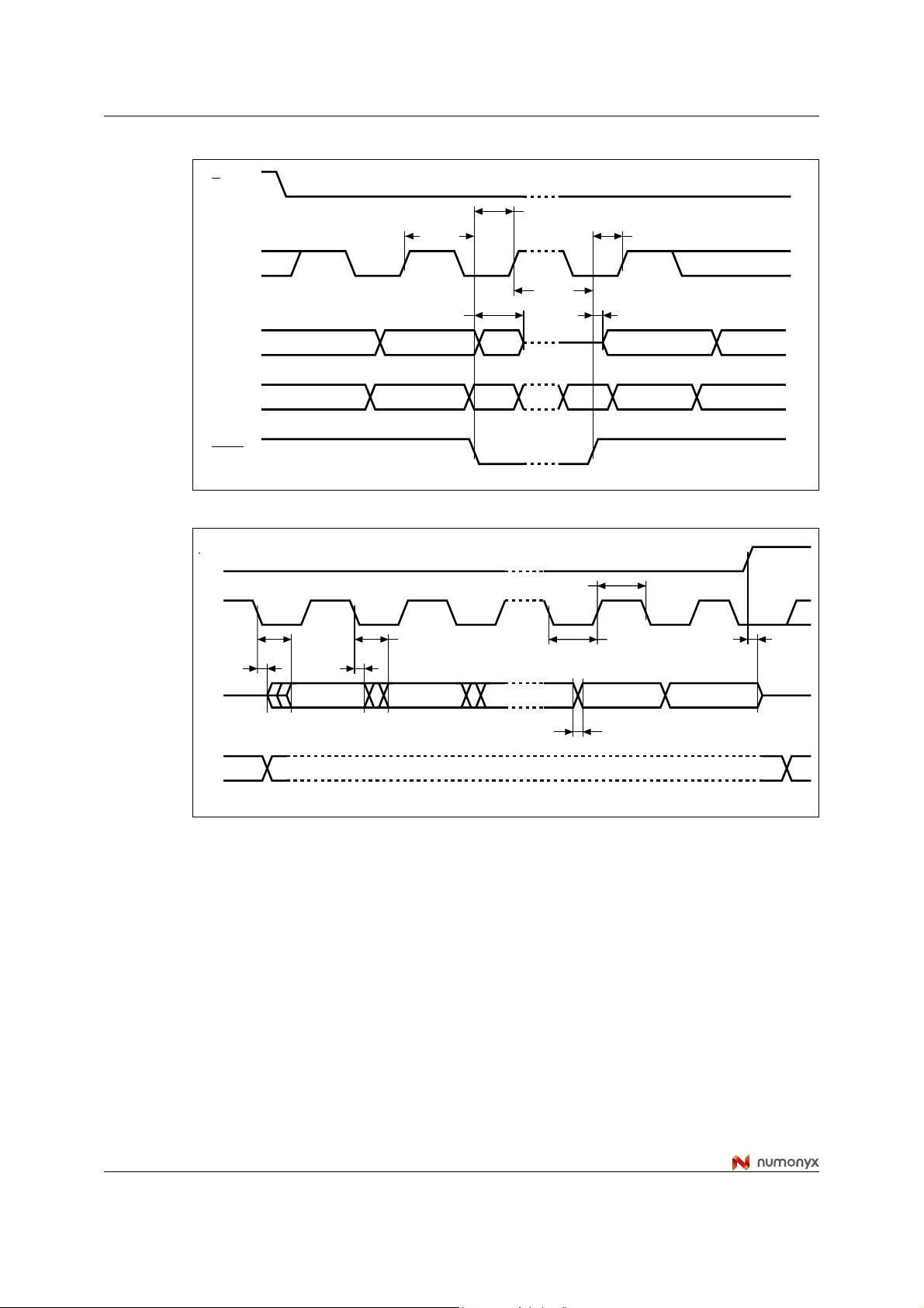
DC and AC parameters M25P05-A
Figure 24. Hold timing
S
tHLCH
tCHHL
C
tCHHH
Q
D
HOLD
tHHCH
tHHQXtHLQZ
AI02032
Figure 25. Output timing
S
C
tCLQX
Q
D
tCLQV
ADDR
.LSB IN
tCLQX
tCLQV
tCH
tCL
tQLQH
tQHQL
tSHQZ
LSB OUT
AI01449e
44/52
Page 45
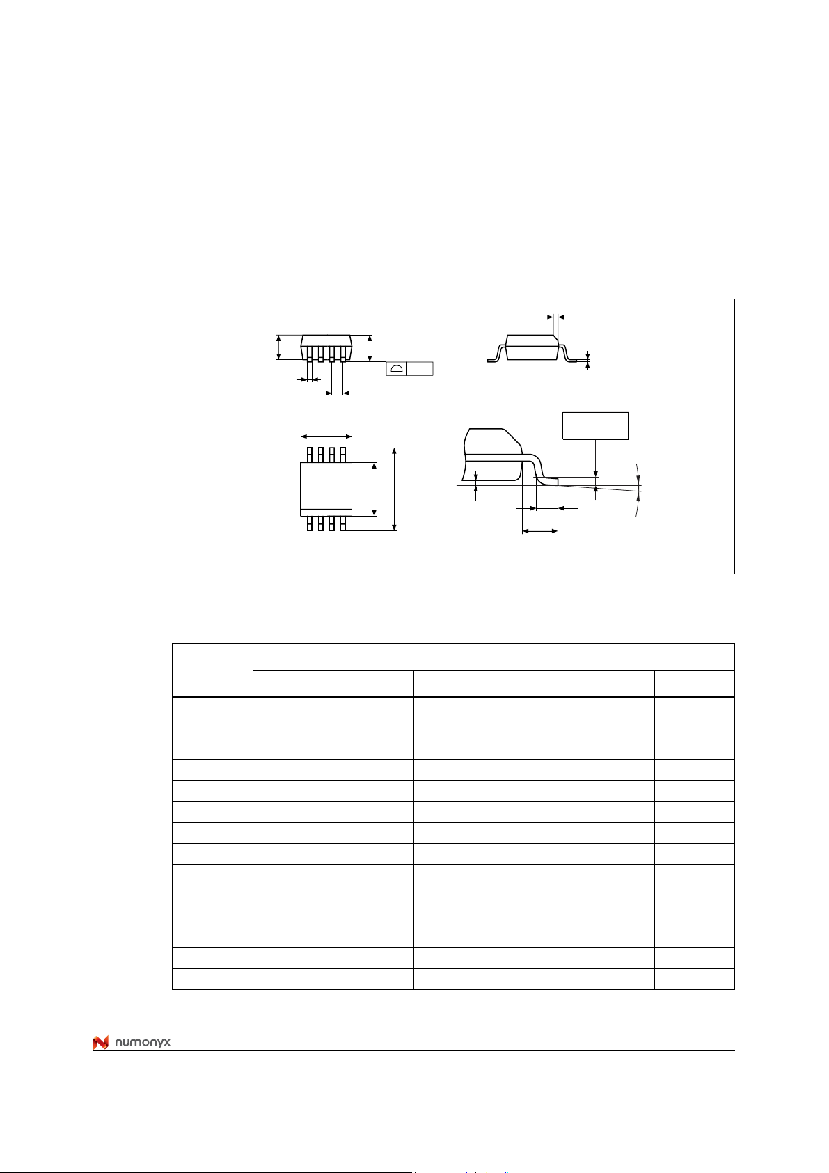
M25P05-A Package mechanical
11 Package mechanical
In order to meet environmen tal requir ements , Numon yx offers these devices in ECOPACK®
packages. These packages have a lead-free second level interconnect. The category of
second level interconnect is marked on the package and on the inner box label, in
compliance with JEDEC Standard JESD97. The maximum ratings related t o soldering
conditions are also marked on the inner bo x label.
Figure 26. SO8N – 8 lead plastic small outline, 150 mils body width, package outline
h x 45˚
A2
b
e
D
8
1
1. Drawing is not to scale.
Table 18. SO8N – 8 lead plastic small outline, 150 mils body width, package
E1
A
ccc
E
A1
L
L1
c
0.25 mm
GAUGE PLANE
k
SO-A
mechanical data
Symbol
Typ Min Max Typ Min Max
A1.750.069
A1 0.10 0.25 0.004 0.010
A2 1.25 0.049
b 0.28 0.48 0.011 0.019
c 0.17 0.23 0.007 0.009
ccc 0.10 0.004
D 4.90 4.80 5.00 0.193 0.189 0.197
E 6.00 5.80 6.20 0.236 0.228 0.244
E1 3.90 3.80 4.00 0.154 0.150 0.157
e1.27– –0.050– –
h 0.25 0.50 0.010 0.020
k0°8°0°8°
L 0.40 1.27 0.016 0.050
L1 1.04 0.041
millimeters inches
45/52
Page 46

Package mechanical M25P05-A
Figure 27. VFQFPN8 (MLP8) - 8 lead very thin fine pitch quad flat package no lead,
6 × 5 mm, package outline
θ
aaa CA
A2
C
ddd
CAB
eE2
M
bbb
b
D2
L
70-ME
B
E
E1
aaa CB
A
2x
A
R1
0.10 CB
A1
A3
D
D1
0.10 CA
1. Drawing is not to scale.
2. The circle in the top view of the package indicates the position of pin 1.
Table 19. VFQFPN8 (MLP8) - 8 lead very thin fine pitch quad flat package no lead,
6 × 5 mm, package mechanical data
millimeters inches
Symbol
Typ Min Max Typ Min Max
A 0.85 0.80 1.00 0.033 0.031 0.039
A1 0.00 0.05 0.000 0.002
A2 0.65 0.026
A3 0.20 0.008
b 0.40 0.35 0.48 0.016 0.014 0.019
D6.00 0.236
D1 5.75 0.226
D2 3.40 3.20 3.60 0.134 0.126 0.142
E5.00 0.197
E1 4.75 0.187
E2 4.00 3.80 4.30 0.157 0.150 0.169
e1.27– –0.050– –
R1 0.10 0.00 0.004 0.000
L 0.60 0.50 0.75 0.024 0.020 0.029
Q 12° 12°
aaa 0.15 0.006
bbb 0.10 0.004
ddd 0.05 0.002
46/52
Page 47

M25P05-A Package mechanical
Figure 28. TSSOP8 – 8 lead thin shrink small outline, package outline
D
8
5
c
EE1
1
CP
4
α
A1
A2A
eb
L
L1
TSSOP8AM
1. Drawing is not to scale.
Table 20. TSSOP8 – 8 lead thin shrink small outline, package mechanical data
millimeters inches
Symbol
Typ Min Max Typ Min Max
A 1.20 0.047
A1 0.05 0.15 0.002 0.006
A2 1.00 0.80 1.05 0.039 0.031 0.041
b 0.19 0.30 0.007 0.012
c 0.09 0.20 0.003 0.008
CP 0.10 0.004
D 3.00 2.90 3.10 0.118 0.114 0.122
e0.65– –0.026– –
E 6.40 6.20 6.60 0.252 0.244 0.260
E1 4.40 4.30 4.50 0.173 0.169 0.177
L 0.60 0.45 0.75 0.024 0.018 0.029
L1 1.00 0.039
α 0° 8° 0° 8°
N8 8
47/52
Page 48

Package mechanical M25P05-A
Figure 29. UFDFPN8 (MLP8) – 8 lead ultra thin fine pitch dual flat package no lead,
2 x 3 mm package outline
e
D
b
L3
E
A
D2
A1
1. Drawing is not to scale.
Table 21. UFDFPN8 (MLP8) – 8 lead ultra thin fine pitch dual flat package no lead,
ddd
L1
E2
L
UFDFPN-01
2 x 3 mm package mechanical data
millimeters inches
Symbol
Typ Min Max Typ Min Max
A 0.55 0.45 0.60 0.022 0.018 0.024
A1 0.02 0.00 0.05 0.001 0.000 0.002
(1)
b
D 2.00 1.90 2.10 0.079 0.075 0.083
D2 1.60 1.50 1.70 0.063 0.059 0.067
(2)
ddd
E 3.00 2.90 3.10 0.118 0.114 0.122
E2 0.20 0.10 0.30 0.008 0.004 0.012
0.25 0.20 0.30 0.010 0.008 0.012
0.08 0.003
e0.50– –0.020– –
L 0.45 0.40 0.50 0.018 0.016 0.020
L1 0.15 0.006
L3 0.30 0.012
1. Dimension b applies to plated terminal and is measured between 0.15 and 0.30 mm from the terminal tip.
2. Applied for exposed die paddle and terminals. Exclude embedding part of exposed die paddle from
measuring.
48/52
Page 49

M25P05-A Ordering information
12 Ordering information
Table 22. Ordering information scheme
Example: M25P05-A V MN 6 T P
Device type
M25P
Device function
05-A = 512 Kbits (64 Kbit x8)
Operating voltage
V = V
= 2.3 to 3.6 V
CC
Package
MN = SO8 (150 mil width)
MP = VFQFPN8 (MLP8)
DW = TSSOP8
(1)
MB = UFDFPN8 (MLP8)
Temperature range
6 = –40 to 85 °C
Option
blank = standard packing
T = tape & reel packing
Plating technology
P or G = ECOPACK® (RoHS compliant)
1. The TSSOP8 package is available in products with process technology code X and Y (details of how to
find the process on the device marking are given in application note AN1995).
Note: For a list of available options (spee d, package, etc.) or f o r fu rther information on any aspect
of this device, please contact your nearest Numonyx sales office.
49/52
Page 50

Revision history M25P05-A
13 Revision history
Table 23. Document revision history
Date Revision Changes
25-Feb-2001 1.0 Initial release.
Clarification of descriptions of entering Standby Power mode from Deep
11-Apr-2002 1.1
12-Sep-2002 1.2 VFQFPN8 package (MLP8) added.
13-Dec-2002 1.3
24-Nov-2003 2
Power-down mode, and of terminating an instruction sequence or dataout sequence.
Typical Page Program time improved. Write Protect setup and hold times
specified, for applications that switch Write Protect to exit the Hardware
Protection mode immediately before a WRSR, and to enter the Hardware
Protection mode again immediately after.
Table of contents, warning about exposed paddle on MLP8, and Pb-free
options added.
40 MHz AC characteristics table included as well as 25 MHz. I
CC3
(max),
tSE(typ) and tBE(typ) values improved. Change of naming for VDFPN8
package
13-Jan-2005 3
01-Apr-2005 4
01-Aug-2005 5
06-Jul-2006 6
19-Dec-2006 7
Devices with process technology code X added (Read identification
(RDID) and Ta ble 17: AC characteristics (50 MHz operation)) added.
TSSOP8 package added.
Notes 1 and 2 removed from Table 22: Ordering information scheme and
Note 1 added.
Note 1 to Table 9: Absolute maximum ratings changed, note 2 and T
LEAD
values removed.
Small text changes.
Frequency test condition modified for I
in Table 13: DC characteristics.
CC3
Read identification (RDID), Deep power-down (DP) and Release from
deep power-down and read electronic signature (RES) instructions and
Active power, standby power and deep power-down modes paragraph
clarified.
SO8 package specifications updated (see Figure 26. and Table 18).
Updated Page Program (PP) instructions in Page programming, Page
program (PP) and Instruction times.
Packages are fully ECOPACK® compliant. SO8N and VFQFPN8 package
specifications updated (see Section 11: Package mechanical).
Figure 3: Bus master and memory devices on the SPI bus updated and
Note 2 added. T
removed from Section Table 9.: Absolute maximum
LEAD
ratings. Small text changes.
VCC supply voltage and VSS ground descriptions added. Figure 3: Bus
master and memory devices on the SPI bus updated, note 2 removed
replaced by explanatory paragraph.
WIP bit behavior at power-up specified in Section 7: Power-up and power-
down. T
added and VIO max modified in Table 9: Absolute maximum
LEAD
ratings. VFQFPN8 and SO8N packages updated (see Section 11:
Package mechanical).
50/52
Page 51

M25P05-A Revision history
Table 23. Document revision history (continued)
Date Revision Changes
Removed ‘low voltage’ from the title. Small text changes.
Changed note below Table 12: Capacitance.
Changed the minimum value for V
UFDFPN8 package (MLP8) added.
07-Aug-2007 8
Frequency test condition modified for I
tSE(typ), tBE(typ) and tPP(typ) values improved in Table 14: Instruction
times.
Changed maximum value for f
operation).
10-Oct-2007 9 Added the reference to a new process technology (code Y).
10-Dec-2007 10 Applied Numonyx branding.
Updated Table 3: Bus master and memory devices on the SPI bus.
18-Apr-2008 11
Modified the code for UFDFPN8 package from ‘ZW’ to ‘MB’.
Minor text changes.
(from 2.7 to 2.3 V).
CC
in Table 13: DC characteristics.
CC3
in Table 17: AC characteristics (50 MHz
R
51/52
Page 52

M25P05-A
Please Read Carefully:
INFORMATION IN THIS DOCUMENT IS PROVIDED IN CONNECTION WITH NUMONYX™ PRODUCTS. NO LICENSE, EXPRESS OR
IMPLIED, BY ESTOPPEL OR OTHERWISE, TO ANY INTELLECTUAL PROPERTY RIGHTS IS GRANTED BY THIS DOCUMENT. EXCEPT
AS PROVIDED IN NUMONYX'S TERMS AND CONDITIONS OF SALE FOR SUCH PRODUCTS, NUMONYX ASSUMES NO LIABILITY
WHATSOEVER, AND NUMONYX DISCLAIMS ANY EXPRESS OR IMPLIED WARRANTY, RELATING TO SALE AND/OR USE OF
NUMONYX PRODUCTS INCLUDING LIABILITY OR WARRANTIES RELATING TO FITNESS FOR A PARTICULAR PURPOSE,
MERCHANTABILITY, OR INFRINGEMENT OF ANY PATENT, COPYRIGHT OR OTHER INTELLECTUAL PROPERTY RIGHT.
Numonyx products are not intended for use in medical, life saving, life sustaining, critical control or safety systems, or in nuclear facility
Numonyx may make changes to specificati ons and product descriptions at any t ime, without notice.
Numonyx, B.V. may have patents or pending patent applications, trademarks, copyrights, or other intellectual property rights that relate to the
presented subject matter. The furnishing of documents and other materials and information does not provide any license, express or implied,
by estoppel or otherwise, to any such patents, trademarks, copyrights, or other intellectual prop erty rights.
Designers must not rely on the absence or characteristics of any features or instructions marked “reserved” or “undefined.” Numonyx reserves
these for future definition and shall have no responsibility whatsoever for conflicts or incompatibilities arising from future changes to them.
Contact your local Numonyx sale s office or your distributor to obt ain the latest specifications and before placing your product order.
Copies of documents which have an order number and are referenced in this document, or other Numonyx literature may be obtained by
visiting Numonyx's website at http://www.numonyx.com.
Numonyx StrataFlash is a trademar k or registered trademark of Numonyx or it s subsidiaries in the United State s and other countries.
*Other names and brands may be claimed as the property of others.
Copyright © 11/5/7, Numonyx, B.V., All Rights Reserved.
applications.
52/52
 Loading...