

Page 1
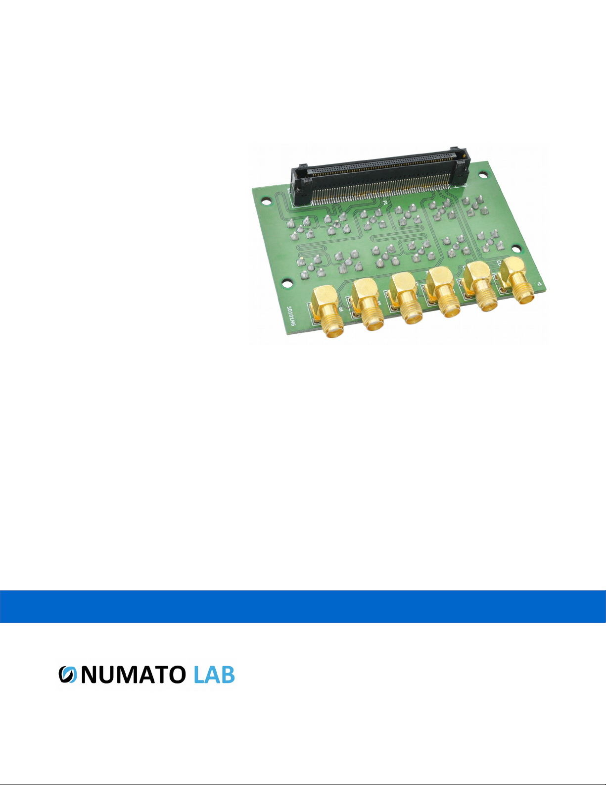
Galatea SMA IO Interconnect Module
User Guide
www.numato.com
Rev 9
Page 2

Get in touch with us!
Please feel free to send a mail to one of the mail IDs below or use the Contact Us page at
http://www.numato.com to drop us a quick message.
Technical Help
Got technical questions? Please write to [email protected]
Sales Team
Questions about making payments, volume discounts, academic/open source discounts, purchase
orders and quotes? Please write to [email protected]
Webmaster
Questions/Suggestions about our website? Please write to [email protected]
Like us on Facebook! https://www.facebook.com/numato
Visit our blog http://www.numato.cc for news, updates and specials.
Mailing Address
Numato Systems Pvt Ltd
1st Floor, #56C Wipro Avenue
Phase 1 - Electronic City
Bangalore, KA-560100, India
* Mail orders, phone orders and direct pick up are not available at this time. Please visit our online store to place your order. Estimated shipping time to
your address will be displayed in the shopping cart before checkout.
You may use, modify or share this publication or part of thereof adhering to Creative
Commons Attribution-ShareAlike 3.0 Unported (CC BY-SA 3.0) License.
See complete license text at http://creativecommons.org/licenses/by-sa/3.0/
All trademarks are property of their respective owners.
Page 3

1 Galatea SMA Module – User Guide
Introduction
Galatea SMA IO Interconnect Module is a SMA breakout solution for Galatea Spartan 6 PCI Express
FPGA Board. This product allows Galatea's IOs and GTP to be broken out in to SMA connectors that
would facilitate easy attachment of other high speed peripherals. The board features 18 SMA
connectors, which include one set of GTP transceiver and 12 IOs. (CLK, RX & TX pairs for GTP is
available only when the module is placed on header P4 in Galatea Spartan 6 PCIe Board)
Board features
• 18 SMA connectors
• 6 SMA connectors for GTP transceivers
• Can be attached to either side of Galatea FPGA board
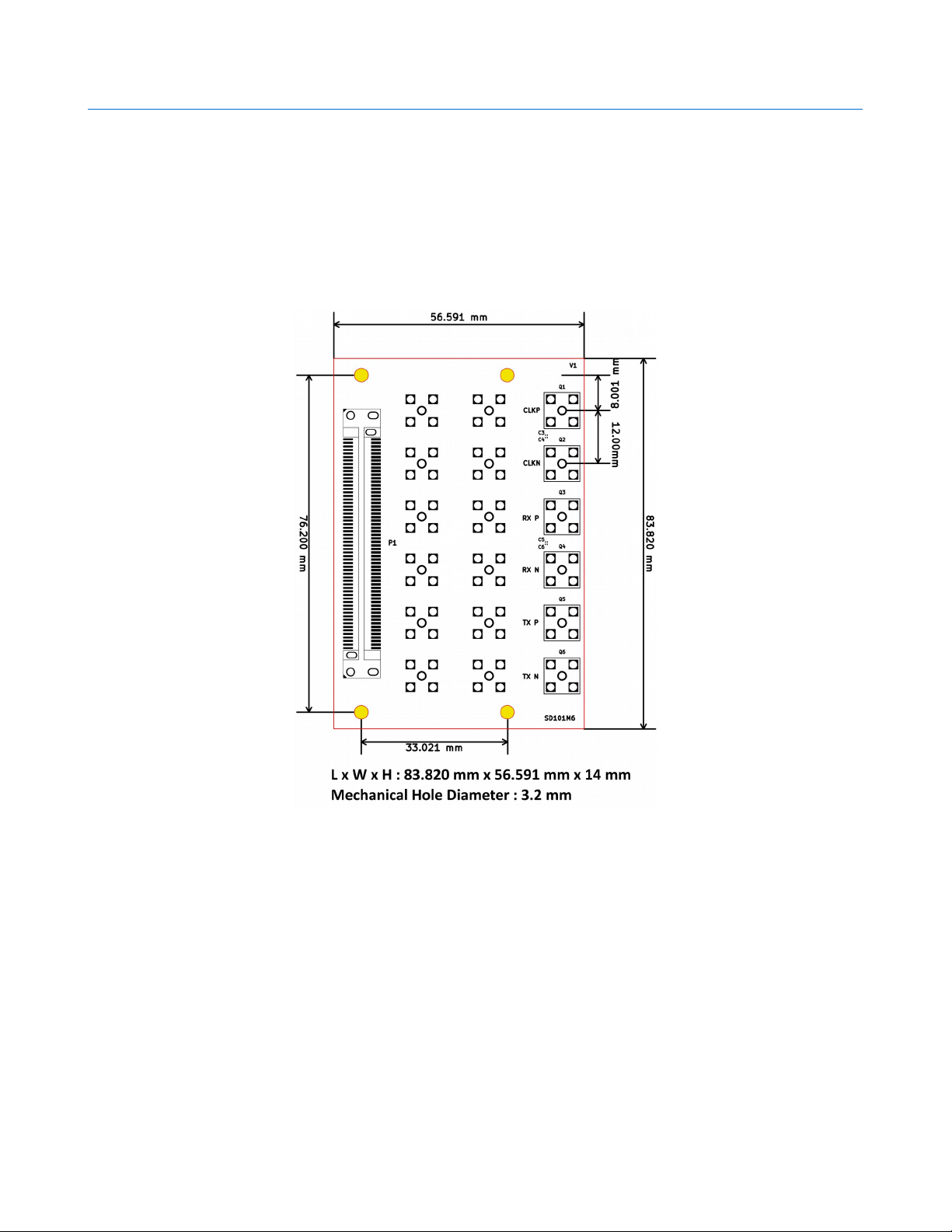
• Dimension: 83.820mm X 56.591mm
©2015 NUMATO SYSTEMS PVT LTD
www.numato.com
Page 4
2 Galatea SMA Module – User Guide
How to use the module
The following section describes how to use this module.
Components/Tools required
Along with the module, you may need the items in the list below for easy and fast installation.
1. Galatea FPGA Development Board.
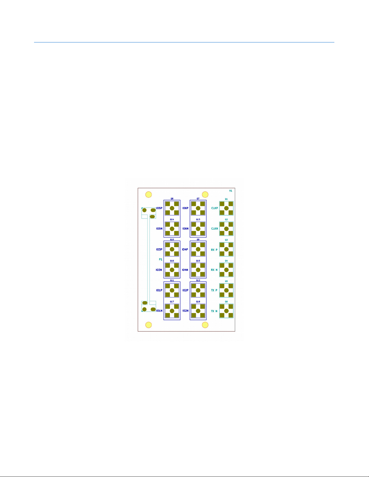
Connection Diagram
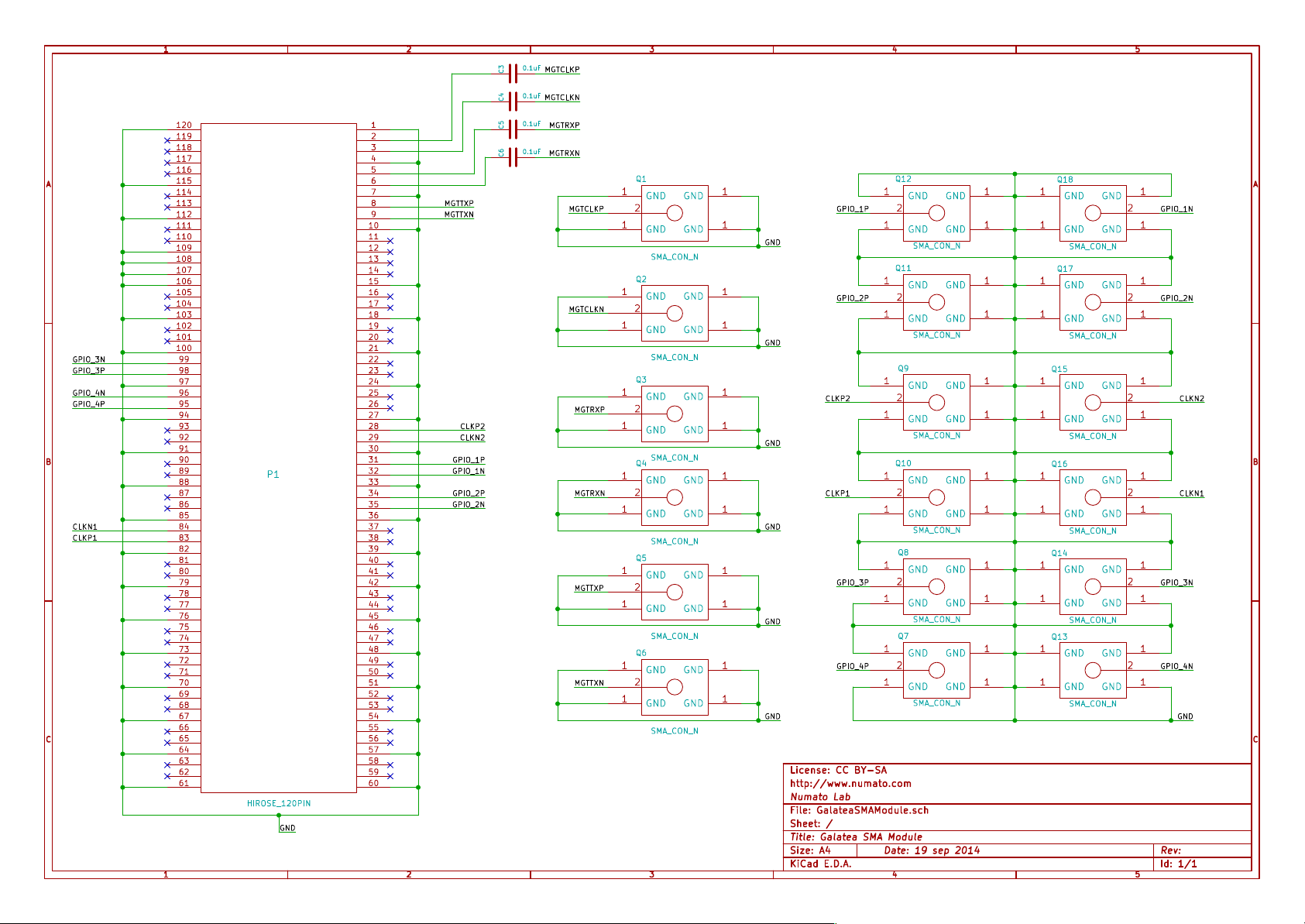
This diagram should be used as a reference only. For detailed information, see the schematics at the
end of this document. Details of individual connectors are as below.
©2015 NUMATO SYSTEMS PVT LTD
www.numato.com
Page 5
3 Galatea SMA Module – User Guide
Connection Details
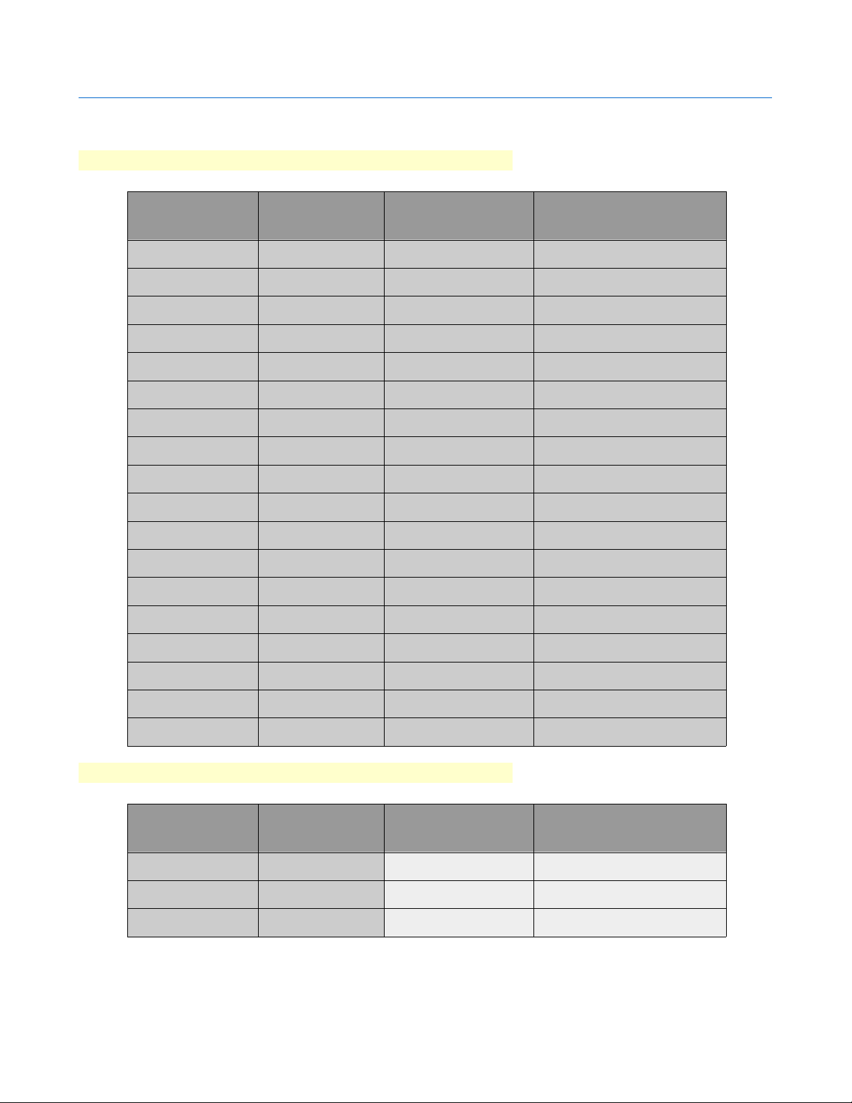
When the SMA Module is placed on the Header P4 on Galatea.
SMA connector Pin Description Spartan-6 (FGG484)
Pin No.
CLKP MGTCLKP C11 MGTREFCLK1P_101
CLKN MGTCLKN D11 MGTREFCLK1N_101
RXP MGTRXP D9 IMGTRXP1_101
RXN MGTRXN C9 MGTRXN1_101
TXP MGTTXP B8 MGTTXP1_101
TXN MGTTXN A8 MGTTXN1_101
Q8 GPIO_3P C19 IO_L64P_SCP5_0
Q14 GPIO_3N A19 IO_L64N_SCP4_0
Q7 GPIO_4P B18 IO_L63P_SCP7_0
Q13 GPIO_4N A18 IO_L63N_SCP6_0
Q9 CLKP2 H12 IO_L35P_GCLK17_0
Q15 CLKN2 G11 IO_L35N_GCLK16_0
Q10 CLKP1 E16 IO_L37P_GCLK13_0
FPGA Pin Description
Q16 CLKN1 F16 IO_L37N_GCLK12_0
Q11 GPIO_2P G8 IO_L32P_0
Q17 GPIO_2N F9 IO_L32N_0
Q12 GPIO_1P H10 IO_L33P_0
Q18 GPIO_1N H11 IO_L33N_0
When the SMA Module is placed on the Header P5 on Galatea.
SMA connector Pin Description Spartan-6 (FGG484)
Pin No.
CLKP MGTCLKP - NC
CLKN MGTCLKN - NC
RXP MGTRXP - NC
FPGA Pin Description
©2015 NUMATO SYSTEMS PVT LTD
www.numato.com
Page 6
4 Galatea SMA Module – User Guide
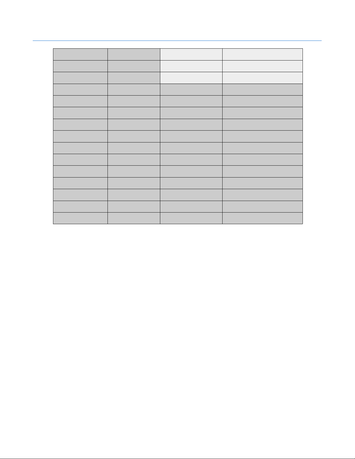
RXN MGTRXN - NC
TXP MGTTXP - NC
TXN MGTTXN - NC
Q8 GPIO_3P V7 IO_L58P_2
Q14 GPIO_3N W8 IO_L58N_2
Q7 GPIO_4P Y7 IO_L47P_2
Q13 GPIO_4N AB7 IO_L47N_2
Q9 CLKP2 AA12 IO_L31P_GCLK31_D14_2
Q15 CLKN2 AB12 IO_L31N_GCLK30_D15_2
Q10 CLKP1 Y11 IO_L32P_GCLK29_2
Q16 CLKN1 AB11 IO_L32N_GCLK28_2
Q11 GPIO_2P AA10 IO_L41P_2
Q17 GPIO_2N AB10 IO_L41N_VREF_2
Q12 GPIO_1P W10 IO_L44P_2
Q18 GPIO_1N Y10 IO_L44N_2
For more information, refer the schematics at the end of this document.
©2015 NUMATO SYSTEMS PVT LTD
www.numato.com
Page 7
5 Galatea SMA Module – User Guide
Technical Specifications
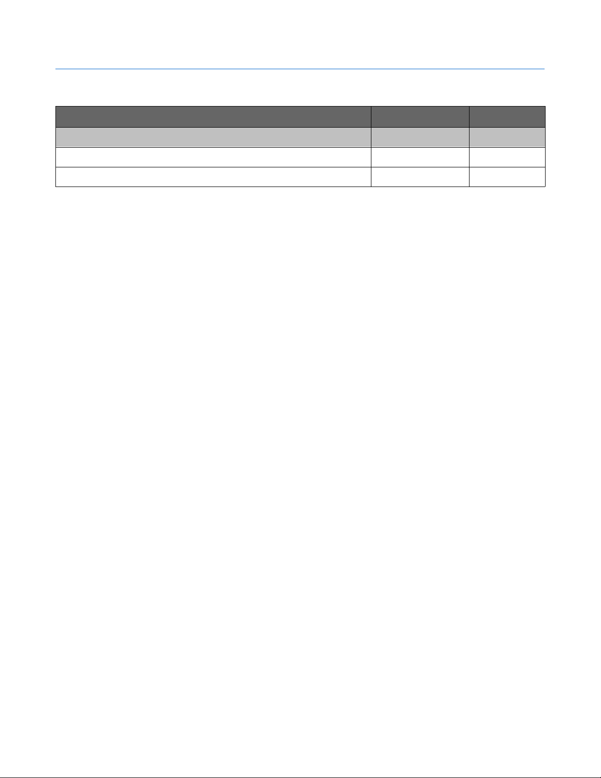
Parameter * Value Unit
Basic Specifications
MGTAVCC 1.2 V
Maximum IO voltage 3.3 V
*All parameters considered nominal. Numato Systems Pvt Ltd reserve the right to modify products without notice.
©2015 NUMATO SYSTEMS PVT LTD
www.numato.com
Page 8
6 Galatea SMA Module – User Guide
Physical Dimensions
Schematics
See next page.
©2015 NUMATO SYSTEMS PVT LTD
www.numato.com
Page 9
1
120
119
118
117
116
A A
GPIO_3N
GPIO_3P
GPIO_4N
GPIO_4P
B B
CLKN1
CLKP1
C C
115
114
113
112
111
110
109
108
107
106
105
104
103
102
101
100
99
98
97
96
95
94
93
92
91
90
89
88
87
86
85
84
83
82
81
80
79
78
77
76
75
74
73
72
71
70
69
68
67
66
65
64
63
62
61
1
P1
HIROSE_120PIN
GND
2
0.1uF
MGTCLKP
C3
0.1uF
MGTCLKN
C4
0.1uF
1
2
3
4
5
6
7
8
9
10
11
12
13
14
15
16
17
18
19
20
21
22
23
24
25
26
27
28
29
30
31
32
33
34
35
36
37
38
39
40
41
42
43
44
45
46
47
48
49
50
51
52
53
54
55
56
57
58
59
60
MGTTXP
MGTTXN
CLKP2
CLKN2
GPIO_1P
GPIO_1N
GPIO_2P
GPIO_2N
MGTRXP
C5
0.1uF
MGTRXN
C6
MGTCLKP
MGTCLKN
MGTRXP
MGTRXN
MGTTXP
MGTTXN
1
1
1
1
1
1
1
1
1
1
1
1
3
Q1
GND
2
GND
SMA_CON_N
Q2
GND
2
GND
SMA_CON_N
Q3
GND
2
GND
SMA_CON_N
Q4
GND
2
GND
SMA_CON_N
Q5
GND
2
GND
SMA_CON_N
Q6
GND
2
GND
SMA_CON_N
GND
GND
GND
GND
GND
GND
GND
GND
GND
GND
GND
GND
4
1
GPIO_1P GPIO_1N
1
GND
1
GPIO_2P
1
GND
1
CLKP2 CLKN2
1
GND
1
1
GND
1
GPIO_3P GPIO_3N
1
GND
1
GPIO_4P GPIO_4N
1
GND
1
1
1
1
1
1
1
1
1
1
1
1
Q12
GND
2
GND
SMA_CON_N
Q11
GND
2
GND
SMA_CON_N
Q9
GND
2
GND
SMA_CON_N
Q10
GND
2
GND
SMA_CON_N
Q8
GND
2
GND
SMA_CON_N
Q7
GND
2
GND
SMA_CON_N
GND
GND
GND
GND
GND
GND
GND
GND
GND
GND
GND
GND
1
1
1
1
1
1
1
1
1
1
1
1
1
1
1
1
1
1
1
1
1
1
1
1
Q18
GND
GND
SMA_CON_N
Q17
GND
GND
SMA_CON_N
Q15
GND
GND
SMA_CON_N
Q16
GND
GND
SMA_CON_N
Q14
GND
GND
SMA_CON_N
Q13
GND
GND
SMA_CON_N
GND
GND
GND
GND
GND
GND
GND
GND
GND
GND
GND
GND
5
1
2
1
1
2
GPIO_2N
1
1
2
1
1
2
CLKN1CLKP1
1
1
2
1
1
2
1
GND
License: CC BY-SA
http://www.numato.com
Numato Lab
File: GalateaSMAModule.sch
Sheet: /
Title: Galatea SMA Module
2
3
KiCad E.D.A.
4
Date: 19 sep 2014
Rev: Size: A4
Id: 1/1
5
 Loading...