ntersema MS5561-C Technical data
MS5561-C
MICRO ALTIMETER
DESCRIPTION
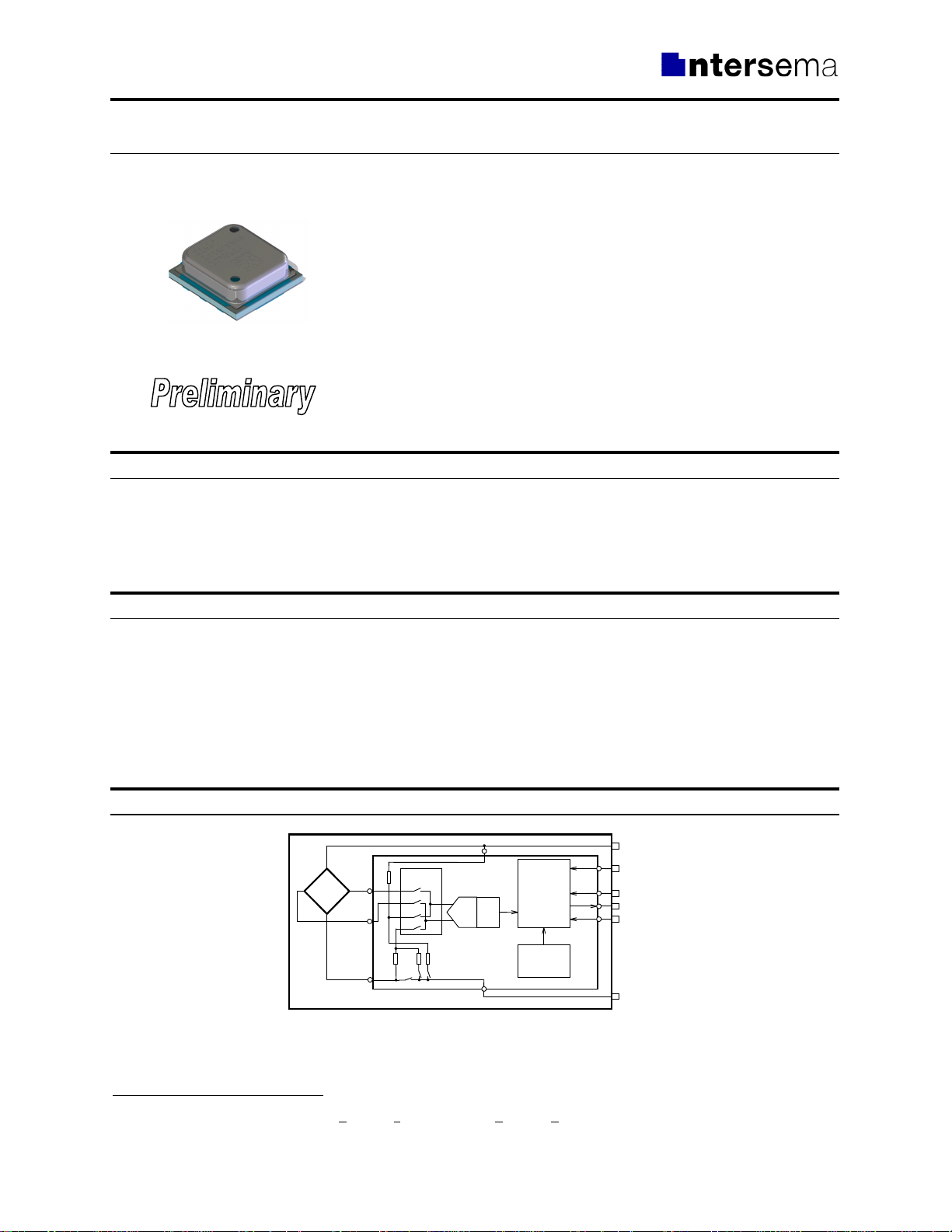
The MS5561 is a SMD-hybrid device including a precision piezo-resistive pressure sensor and an ADC-Interface
IC. It uses a three-wire serial interface for communication. The module dimensions of 4.75 mm x 4.25 mm and a
height of only 1.6 mm allows for up-to-date SMD design. It provides a 16 bit data word from a pressure and
temperature dependent voltage. The MS5561 is a low power, low voltage device with automatic power down
(ON/OFF) switching. A 3-wire interface is used for all communications with a micro-controller.
• 10 - 1100 mbar / 1 – 110 kPa absolute pressure range
• High accuracy temperature measurement
• Integrated miniature pressure sensor module
4.75 mm x 4.25 mm
• Thin design of 1.6 mm
• Piezo-resistive silicon micro-machined sensor
• 6 coefficients for software compensation stored on-
chip
• 16 bit ADC, sigma delta converter
• 3-wire serial interface
• 1 system clock line (32.768 kHz)
• Low voltage and low power consumption
•
RoHS-compatible & Pb-free
*
FEATURES APPLICATIONS
• Pressure resolution 0.1 mbar
• Operating temperature -40°C to +85°C
• Supply voltage 2.2 V to 3.6 V
• Low supply current, typ. 4 µA
Standby current < 0.1 µA
• Calibrated temperature and pressure sensor for
nd
order compensation
2
• ESD protected, HBM 4 kV
• Mobile phones
• GPS receivers
• Altimeter applications
• Personal Navigation Devices (PND)
• Digital cameras with altimeter function
BLOCK DIAGRAM
SENSOR
+IN
-IN
SGND
Input MUX
dig.
ADC
Filter
Sensor
Interface IC
Fig. 1: Block diagram MS5561
Digital
Interface
Memory
(PROM)
64 bits
VDD
MCLK
DIN
DOUT
SCLK
GND
*
The European RoHS directive 2002/95/EC (Restriction of the use of certain Hazardous Substances in electrical and electronic equipment) bans
the use of lead, mercury, cadmium, hexavalent chromium and polybrominated biphenyls (PBB) or polybrominated diphenyl ethers (PBDE).
DA5561_03 January 5, 2009 1
000055611126 – ECN1158
www.sensorway.cn
PIN CONFIGURATION
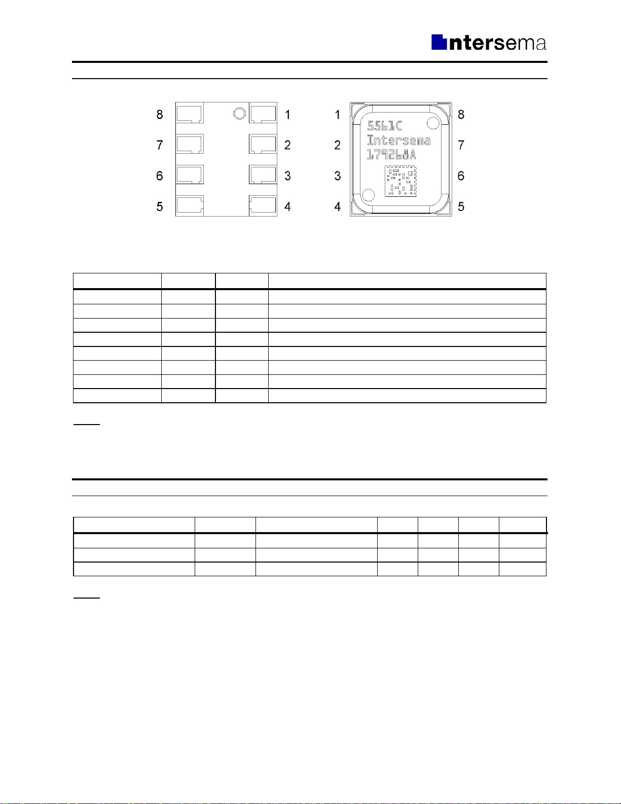
Fig. 2: Pin configuration of MS5561
Pin Name Pin Type Function
SCLK 1 I Serial data clock
GND 2 G Ground
PV (1) 3 N Negative programming voltage
PEN (1) 4 I Programming enable
VDD 5 P Positive supply voltage
MCLK 6 I Master clock (32.768 kHz)
DIN 7 I Serial data input
DOUT 8 O Serial data output
NOTE
1) Pin 3 (PV) and PIN 4 (PEN) are only used by the manufacturer for calibration purposes and should not be
connected.
ABSOLUTE MAXIMUM RATINGS
Parameter Symbol Conditions Min Max Unit Notes
Supply voltage VDD Ta = 25 °C -0.3 4 V
Storage temperature TS -40 +85 °C 1
Overpressure P Ta = 25 °C 10 bar
NOTE
1) Storage and operation in an environment of dry and non-corrosive gases.
DA5561_03 January 5, 2009 2
000055611126 – ECN1158
www.sensorway.cn
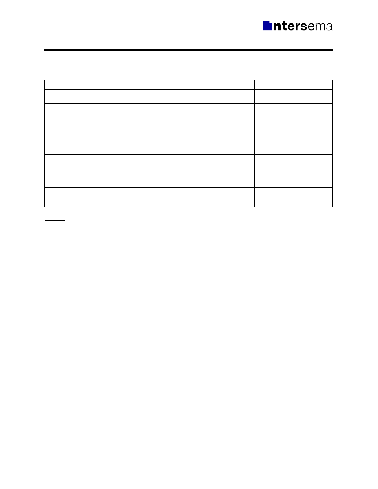
RECOMMENDED OPERATING CONDITIONS
(Ta = 25°C, VDD = 3.0 V unless noted otherwise)
Parameter Symbol Conditions Min. Typ Max Unit
Operating pressure range p 10 1100
Supply voltage VDD 2.2 3.0 3.6 V
Supply current,
average (1)
during conversion (2)
standby (no conversion)
Current consumption into
MCLK (3)
Operating temperature
range
Conversion time t
I
avg
I
sc
Iss
T -40 +25 +85 °C
MCLK = 32.768 kHz 35 ms
conv
VDD = 3.0 V
4
1
0.1
MCLK = 32.768 kHz 0.5
External clock signal (4) MCLK 30.000 32.768 35.000 kHz
Duty cycle of MCLK 40/60 50/50 60/40 %
Serial data clock SCLK 500 kHz
NOTES
1) Under the assumption of one conversion every second. Conversion means either a pressure or a
temperature measurement started by a command to the serial interface of MS5561.
2) During conversion the sensor will be switched on and off in order to reduce power consumption; the total on
time within a conversion is about 2 ms.
3) This value can be reduced by switching off MCLK while MS5561 is in standby mode.
4) It is strongly recommended that a crystal oscillator be used because the device is sensitive to clock jitter. A
square-wave form of the clock signal is a must.
mbar
abs.
µA
mA
µA
µA
DA5561_03 January 5, 2009 3
000055611126 – ECN1158
www.sensorway.cn
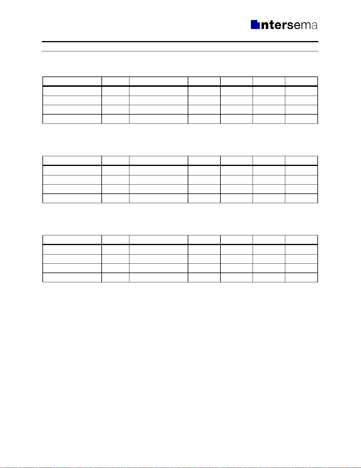
ELECTRICAL CHARACTERISTICS
DIGITAL INPUTS
(T = -40°C .. 85°C, VDD = 2.2 V .. 3.6 V)
Parameter Symbol Conditions Min Typ Max Unit
Input High Voltage VIH 80% VDD 100% VDD
Input Low Voltage VIL 0% VDD 20% VDD V
Signal Rise Time tr 200 ns
Signal Fall Time tf 200 ns
DIGITAL OUTPUTS
(T = -40°C .. 85°C, VDD = 2.2 V .. 3.6 V)
Parameter Symbol Conditions Min Typ Max Unit
Output High Voltage VOH I
Output Low Voltage VOL I
Signal Rise Time tr 200 ns
Signal Fall Time tf 200 ns
AD-CONVERTER
Parameter Symbol Conditions Min Typ Max Unit
Resolution 16 bit
Linear Range 4’000 40’000 LSB
Conversion Time MCLK = 32.768 kHz 35 ms
INL Within linear range -5 +5 LSB
= 0.6 mA 80% VDD 100% VDD
source
= 0.6 mA 0% VDD 20% VDD V
sink
(T = -40°C .. 85°C, VDD = 2.2 V .. 3.6 V)
V
V
DA5561_03 January 5, 2009 4
000055611126 – ECN1158
www.sensorway.cn
PRESSURE OUTPUT CHARACTERISTICS
With the calibration data stored in the interface IC of the MS5561, the following characteristics can be achieved:
(VDD = 3.0 V unless noted otherwise)
Parameter Conditions Min Typ Max Unit Notes
Resolution
Absolute Pressure Accuracy
Relative Pressure Accuracy
p = 300 .. 1000 mbar
= 25°C
T
a
p = 750 .. 1100 mbar
= 25°C
T
a
p = 750 .. 1100 mbar
= 25°C
T
a
T = 0 .. +50°C
Relative Pressure Error over
Temperature
p = 300 .. 1000 mbar
T = -40 .. +85°C
p = 300 .. 1000 mbar
Long-term Stability 12 months -1 mbar 5
Maximum Error over Supply
Voltage
VDD = 2.2 .. 3.6 V
p = const.
NOTES
1) A stable pressure reading of the given resolution requires taking the average of 2 to 4 subsequent pressure
values due to noise of the ADC.
2) Maximum error of pressure reading over the pressure range.
3) Maximum error of pressure reading over the pressure range after offset adjustment at one pressure point.
4) With the second-order temperature compensation as described in Section “FUNCTION". See next section for
typical operating curves.
5) The long-term stability is measured with non-soldered devices.
0.1 mbar 1
-1.5 +1.5 mbar 2
-0.5 +0.5 mbar 3
-1 +1 mbar 4
-2 +3 mbar 4
-1.6 +1.6 mbar
TEMPERATURE OUTPUT CHARACTERISTICS
This temperature information is not required for most applications, but it is necessary to allow for temperature
compensation of the pressure output.
(VDD = 3.0 V unless noted otherwise)
Parameter Conditions Min Typ Max Unit Notes
Resolution 0.005 0.01 0.015 °C
Accuracy
Maximum Error over Supply
Voltage
NOTES
1) With the second-order temperature compensation as described in Section “FUNCTION". See next section for
typical operating curves.
2) At Ta = 25 °C
T = 20°C -0.8 0.8 °C
T = -40 .. +85°C -2 +3 °C 1
VDD = 2.2 .. 3.6 V -0.2 + 0.2 °C 2
DA5561_03 January 5, 2009 5
000055611126 – ECN1158
www.sensorway.cn
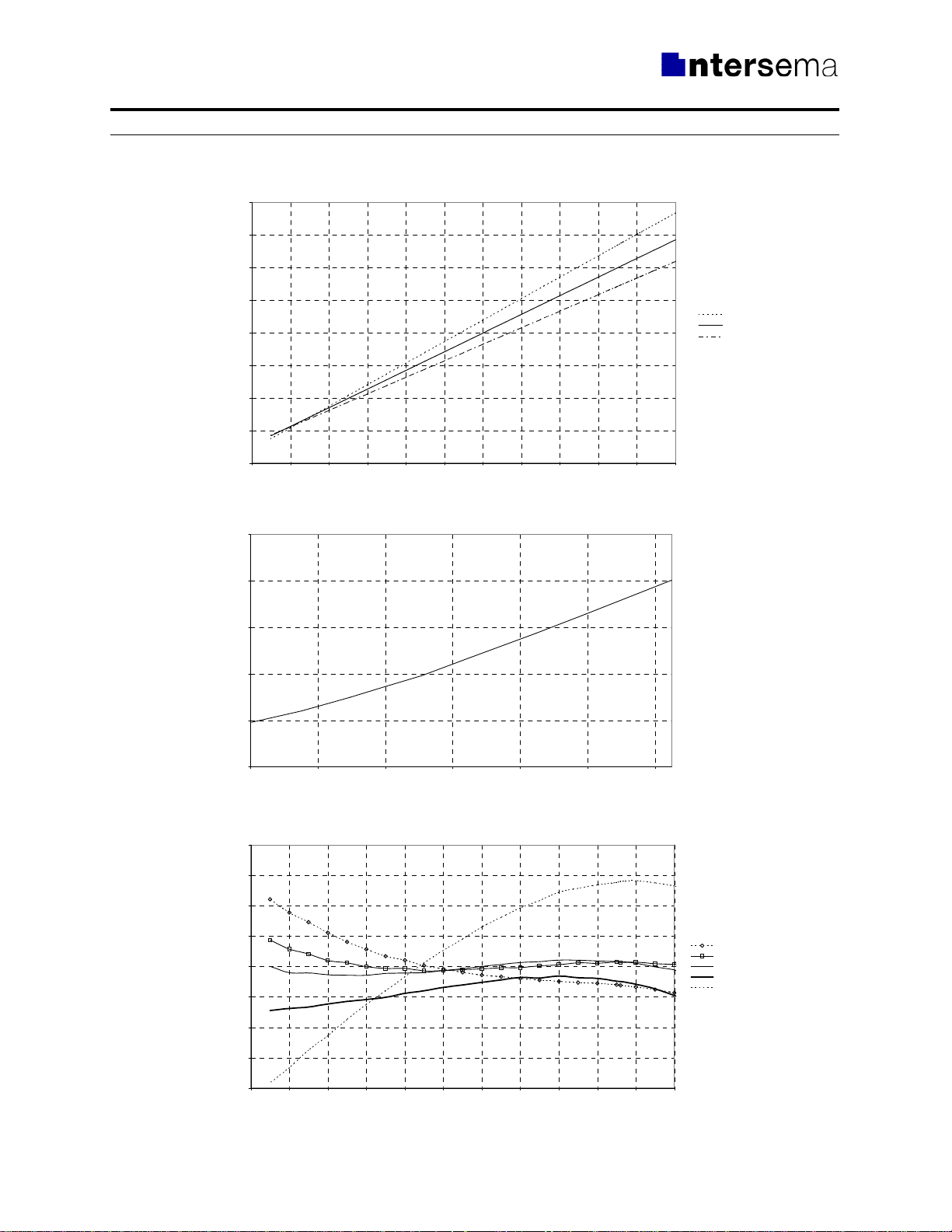
TYPICAL PERFORMANCE CURVES
ADC-value D1 vs Pressure (typical)
22000
20000
18000
16000
14000
ADC-value D1 (LSB)
12000
10000
8000
6000
0 100 200 300 400 500 600 700 800 900 1000 1100
ADC-value D2 vs Temperature (typical)
40000
35000
Pressure (mbar)
-40°C
25°C
85°C
30000
25000
ADC-value D2 (LSB)
20000
15000
-40 -2 0 0 20 40 60 80
Absolute Pressure Accuracy after Calibration, 2nd order compensation
4
3
2
1
0
-1
Pressure error (mbar)
-2
-3
Temperature (°C)
85°C
60°C
25°C
0°C
-40°C
-4
0 100 200 300 400 500 600 700 800 900 1000 1100
DA5561_03 January 5, 2009 6
000055611126 – ECN1158
Pressure (mbar)
www.sensorway.cn
