

NTE NTE997 Datasheet
NTE997
Integrated Circuit
Quad Operational Amplifier
Description:
The NTE997 is a monolithic quad operational amplifier in a 14–Lead DIP type package consisting of
four independent high gain, internally compensated operational amplifiers. The specifically designed
low noise input transistors allow the NTE997 to be used in low noise signal processing applications
such as audio preamplifiers and signal conditioners. The simplified output stage completely eliminates crossover distortion under any load conditions, has large source and sink capacity, and is short–
circuit protected. A novel current source stabilizes output parameters over a wide power supply voltage range.
Features:
D Unity Gain Bandwidth: 3MHz
D Continuous Short Circuit Protection
D No Frequency Compensation Required
D No Latch–Up
D Large Common Mode and Differential Voltage Ranges
D Parameter Tracking Over Temperature Range
D Gain and Phase Match Between Amplifiers
Absolute Maximum Ratings:
Supply Voltage ±18V. . . . . . . . . . . . . . . . . . . . . . . . . . . . . . . . . . . . . . . . . . . . . . . . . . . . . . . . . . . . . . . . . . . .
Differential Input Voltage (Note 1) ±30V. . . . . . . . . . . . . . . . . . . . . . . . . . . . . . . . . . . . . . . . . . . . . . . . . . .
Input Voltage (Note 1) ±15V. . . . . . . . . . . . . . . . . . . . . . . . . . . . . . . . . . . . . . . . . . . . . . . . . . . . . . . . . . . . . .
Internal Power Dissipation (T
Derate Above 70°C 8.3mW/°C. . . . . . . . . . . . . . . . . . . . . . . . . . . . . . . . . . . . . . . . . . . . . . . . . . . . .
Output Short Circuit Duration (Note 2) Indifinite. . . . . . . . . . . . . . . . . . . . . . . . . . . . . . . . . . . . . . . . . . . .
Operating Temperature Range –55° to +125°C. . . . . . . . . . . . . . . . . . . . . . . . . . . . . . . . . . . . . . . . . . . . .
Storage Temperature Range –55° to +125°C. . . . . . . . . . . . . . . . . . . . . . . . . . . . . . . . . . . . . . . . . . . . . . .
Lead Temperature (During Soldering, 10sec) +260°C. . . . . . . . . . . . . . . . . . . . . . . . . . . . . . . . . . . . . . .
Note 1. For supply voltage less than ±15V , the absolute maximum input voltage is equal to the supply
voltage.
Note 2. Short–circuit may be to GND, one amplifier only. I
= +70°C) 670mW. . . . . . . . . . . . . . . . . . . . . . . . . . . . . . . . . . . . . . . . . . .
A
= 45mA (Typical).
SC
Electrical Characteristics: (TA = +25°C, VS = ±15V unless otherwise specified)
Parameter Test Conditions Min Typ Max Unit
Input Offset Voltage RS ≤ 10kΩ – 0.5 5.0 mV
RS ≤ 10kΩ, –55° ≤ TA ≤ +125°C – – 6.0 mV
Input Offset Current – 5 200 nA
–55° ≤ TA ≤ +125°C – – 500 nA
Input Bias Current – 40 500 nA
–55° ≤ TA ≤ +125°C – – 1500 nA
Input Resistance 0.3 5.0 – MΩ
Large Signal Voltage Gain RL ≥ 2kΩ, V
RL ≥ 2kΩ, V
+125°C
Output Voltage Swing RL ≥ 10kΩ ±12 ±14 – V
RL ≥ 2kΩ ±10 ±13 – V
RL ≥ 2kΩ, –55° ≤ TA ≤ +125°C ±12 – – V
Input Voltage Range ±12 ±14 – V
Common Mode Rejection Ratio RS ≤ 10kΩ 70 90 – dB
Supply Voltage Rejection Ratio RS ≤ 10kΩ – 30 150 µV/V
Power Consumption – 210 340 mW
TA = –55°C – 240 400 mW
TA = +125°C – 180 300 mW
Transient Response (Unity Gain) Overshoot VIN = 20mV, RL = 2kΩ, CL ≤ 100pF – 5.0 – %
Unity Gain Bandwidth 2.0 3.0 – MHz
Slew Rate (Unity Gain) RL ≥ 2kΩ – 1.5 – V/µs
Channel Separation (Open Loop) f = 10kHz, RS = 1kΩ, Gain = 100 – 105 – dB
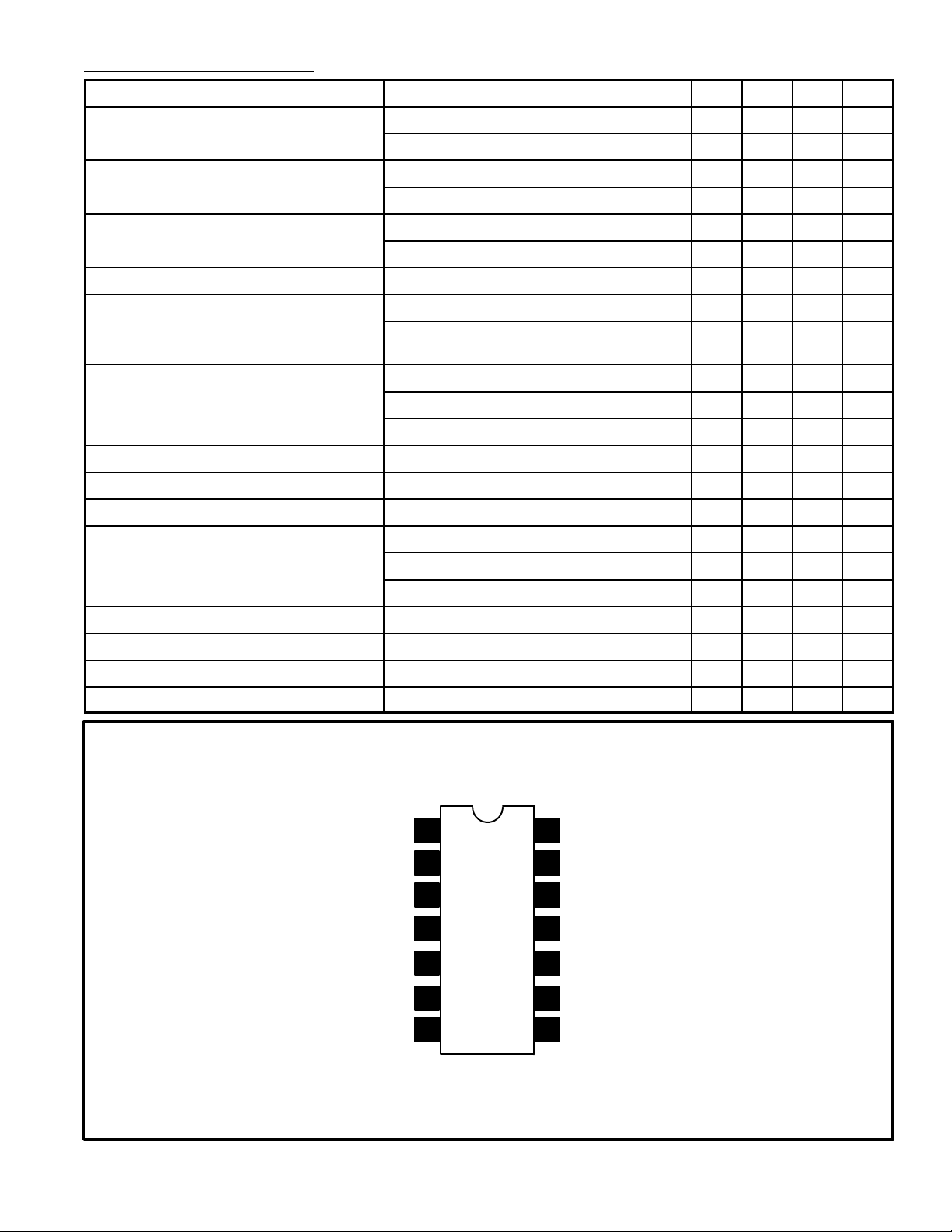
Pin Connection Diagram
= ±10V 50k 300k –
OUT
= ±10V, –55° ≤ TA ≤
OUT
25k – –
Invert Input A Invert Input D
Non–Invert Input A
Output A
Output B
Non–Invert Input B
Invert Input B
(–) V
CC
1
2
3
4
5
6
7
14
Non–Invert Input D
13
Output D
12
(+) V
11
Output C
10
9
Non–Invert Input C
8
Invert Input C
CC
 Loading...