

NTE NTE996 Datasheet

NTE996
Linear Integrated Circuit
Operational Transconductance Amplifier
Description:
The NTE996 is a programmable transconductance block intended to fulfill a wide variety of variable
gain applications. This device has differential inputs and high impedance push–pull outputs. The
NTE996 has high input impedance and its transconductance (g
fier bias current (I
ABC
).
High slew rate together with programmable gain make the NTE996 an ideal choice for variable gain
applications such as sample and hold, multiplexing, filtering, and multiplying,
Features:
D Slew Rate (Unity Gain Compensated): 50V/µs
) is directly proportional to the ampli-
m
D Fully Adjustable Gain: 0 to g
D Extended g
Linearity: 3 Decades
m
• RL Limit
m
D Flexible Supply Voltage Range: ±2V to ±18V
D Adjustable Power Consumption
Absolute Maximum Ratings:
DC Supply Voltage, V
Power Dissipation, P
S
D
250mW. . . . . . . . . . . . . . . . . . . . . . . . . . . . . . . . . . . . . . . . . . . . . . . . . . . . . . . . . .
Differential Input Voltage ±5V. . . . . . . . . . . . . . . . . . . . . . . . . . . . . . . . . . . . . . . . . . . . . . . . . . . . . . . . . . . .
Amplifier Bias Current, I
DC Input Voltage +V
. . . . . . . . . . . . . . . . . . . . . . . . . . . . . . . . . . . . . . . . . . . . . . . . . . . . . . . . . . . . .
ABC
to –V
S
Output Short Circuit Duration Indefinite. . . . . . . . . . . . . . . . . . . . . . . . . . . . . . . . . . . . . . . . . . . . . . . . . . .
Operating Temperature Range, T
Storage Temperature Range, T
opr
stg
Lead Temperature (During Soldering, 10sec), T
L
0° to +70°C. . . . . . . . . . . . . . . . . . . . . . . . . . . . . . . . . . . . . . . . . . .
–65° to +150°C. . . . . . . . . . . . . . . . . . . . . . . . . . . . . . . . . . . . . . . . . .
+260°C. . . . . . . . . . . . . . . . . . . . . . . . . . . . . . . . . . . .
±18V. . . . . . . . . . . . . . . . . . . . . . . . . . . . . . . . . . . . . . . . . . . . . . . . . . . . . . . . . . . . .
2mA. . . . . . . . . . . . . . . . . . . . . . . . . . . . . . . . . . . . . . . . . . . . . . . . . . . . . . . . .
S
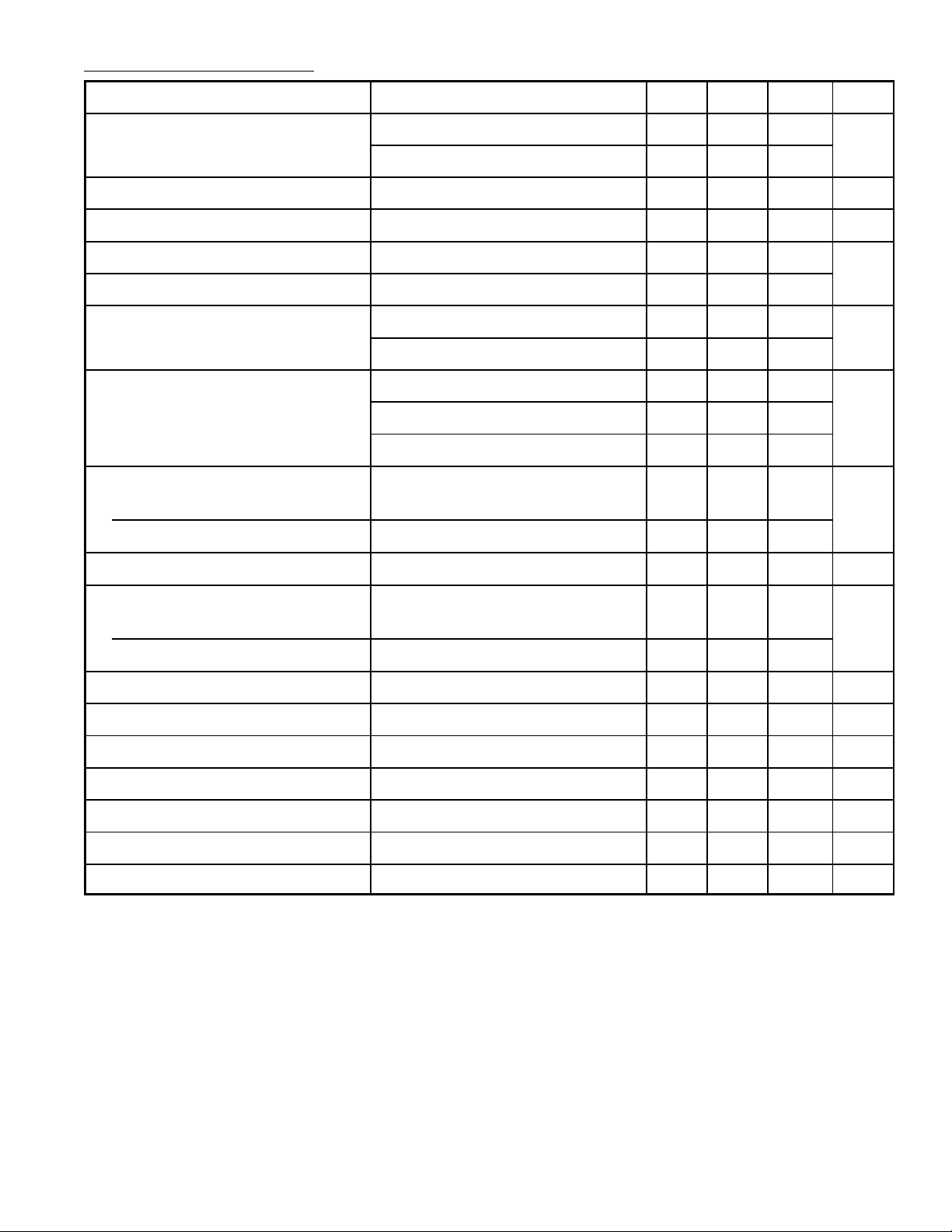
Electrical Characteristics: (VS = ±15V, I
= 500µA, TA = +25°C unless otherwise specified)
ABC
Parameter
Test Conditions Min Typ Max Unit
Input Offset Voltage – 0.4 5.0 mV
TA = 0° to +70°C, I
Input Offset Voltage Charge 5µA ≤ I
≤ 500µA – 0.1 – mV
ABC
= 5µA – 0.3 –
ABC
Input Offset Current – 0.1 – µA
Input Bias Current – 0.4 5.0 µA
TA = 0° to +70°C – 1.0 7.0
Forward Transconductance (gm) 6700 9600 13000 µmho
TA = 0° to +70°C 5400 – –
Peak Output Current RL = 0, I
= 5µA – 5 – µA
ABC
RL = 0 350 500 650
RL = 0, TA = 0° to +70°C 300 – –
Peak Output Voltage
Positive
RL = ∞, 5µA ≤ I
Negative RL = ∞, 5µA ≤ I
≤ 500µA +12.0 +14.2 –
ABC
≤ 500µA –12.0 –14.4 –
ABC
V
Amplifier Supply Current – 1.1 – mA
Input Offset Voltage Sensitivity
Positive
Negative ∆V
∆V
OFFSET
OFFSET
/∆V+ – 20 150
/∆V– – 20 150
µV/V
Common Mode Rejection Ratio 80 110 – dB
Common Mode Range ±12 ±14 – V
Input Resistance 10 26 – kΩ
Magnitude of Leakage Current I
Differential Input Current I
= 0 – 0.2 100 nA
ABC
= 0, Input = ±4V – 0.02 100 nA
ABC
Open Loop Bandwidth – 2.0 – MHz
Slew Rate Unity Gain Compensated – 50 – V/µs
 Loading...