

NTE NTE995M Datasheet

NTE995 & NTE995M
Integrated Circuit
Frequency–to–Voltage Converter
Description:
The NTE995 (14–Lead DIP) and NTE995M (8–Lead DIP) are monolithic frequency to voltage converters with a high gain OP amp/comparator designed to operate a relay, lamp, or other load when
the input frequency reaches or exceeds a selected rate. The tachometer uses a charge pump technique and offers frequency doubling for low ripple, full input protection, and its output swings to GND
for a zero frequency input.
Advantages:
D Output Swing to GND for Zero Frequency Input
D Easy to Use: V
D Only One RC Network Provides Frequency Doubling
D Zener Regulator On Chip Allows Accurate and Stable Frequency to Voltage or Current Conversion
Features:
D Ground Referenced Tachometer Input Interfaces Directly with Variable Reluctance Magnetic
Pickups
D OP Amp/Comparator has Floating Transistor Output
D 50mA Sink or Source to Operate Relays, Solenoids, Meters, or LEDs
D Frequency Doubling for Low Ripple
D Tachometer has Built–In Hysteresis with Either Differential Input or Ground Referenced Input
D Built–In Zener Diode
D ±0.3% Linearity Typical
D Ground Referenced Tachometer is Fully Protected from damage Due to Swings Above V
and Below GND
= fIN x VCC x R1 x C1
OUT
CC
Applications:
D Over/Under Speed Sensing
D Frequency to Voltage Conversion (Tachometer)
D Speedometers
D Breaker Point Dwell Meters
D Hand–Held Tachometer
D Speed Governors
D Cruise Control
D Automotive Door Lock Control
D Clutch Control
D Horn Control
D Touch or Sound Switches
Absolute Maximum Ratings:
Supply Voltage, V
CC
Supply Current (Zener Options) 25mA. . . . . . . . . . . . . . . . . . . . . . . . . . . . . . . . . . . . . . . . . . . . . . . . . . . .
Collector Voltage 28V. . . . . . . . . . . . . . . . . . . . . . . . . . . . . . . . . . . . . . . . . . . . . . . . . . . . . . . . . . . . . . . . . . .
Differential Input Voltage
Tachometer 28V. . . . . . . . . . . . . . . . . . . . . . . . . . . . . . . . . . . . . . . . . . . . . . . . . . . . . . . . . . . . . . . . . .
OP Amp/Comparator 28V. . . . . . . . . . . . . . . . . . . . . . . . . . . . . . . . . . . . . . . . . . . . . . . . . . . . . . . . .
Input Voltage Range
Tachometer
NTE995M ±28V. . . . . . . . . . . . . . . . . . . . . . . . . . . . . . . . . . . . . . . . . . . . . . . . . . . . . . . . . . . . . . .
NTE955 0.0V to +28V. . . . . . . . . . . . . . . . . . . . . . . . . . . . . . . . . . . . . . . . . . . . . . . . . . . . . . . . . .
OP Amp/Comparator 0.0V to +28V. . . . . . . . . . . . . . . . . . . . . . . . . . . . . . . . . . . . . . . . . . . . . . . . .
Power Dissipation (Note 1), P
D
NTE995M 1200mW. . . . . . . . . . . . . . . . . . . . . . . . . . . . . . . . . . . . . . . . . . . . . . . . . . . . . . . . . . . . . .
NTE995 1580mW. . . . . . . . . . . . . . . . . . . . . . . . . . . . . . . . . . . . . . . . . . . . . . . . . . . . . . . . . . . . . . . .
Operating Temperature Range, T
Storage Temperature Range, T
Lead Temperature, T
L
stg
opr
–40° to +85°C. . . . . . . . . . . . . . . . . . . . . . . . . . . . . . . . . . . . . . . . .
–65° to +150°C. . . . . . . . . . . . . . . . . . . . . . . . . . . . . . . . . . . . . . . . . .
NTE995, NTE995M (During Soldering, 10sec) +260°C. . . . . . . . . . . . . . . . . . . . . . . . . . . . . . . .
NTE995M
(Vapor Phase, 60sec) +215°C. . . . . . . . . . . . . . . . . . . . . . . . . . . . . . . . . . . . . . . . . . . . . . . . . . .
(Infrared, 15sec) +220°C. . . . . . . . . . . . . . . . . . . . . . . . . . . . . . . . . . . . . . . . . . . . . . . . . . . . . . .
28V. . . . . . . . . . . . . . . . . . . . . . . . . . . . . . . . . . . . . . . . . . . . . . . . . . . . . . . . . . . . . . . .
Note 1. For operation in ambient temperatures above 25°C, the device must be derated based on
a +150°C maximum junction temperature and a thermal resistance of +101°C/W junction to
ambient for the NTE995M, and +79°C/W junction to ambient for the NTE995.
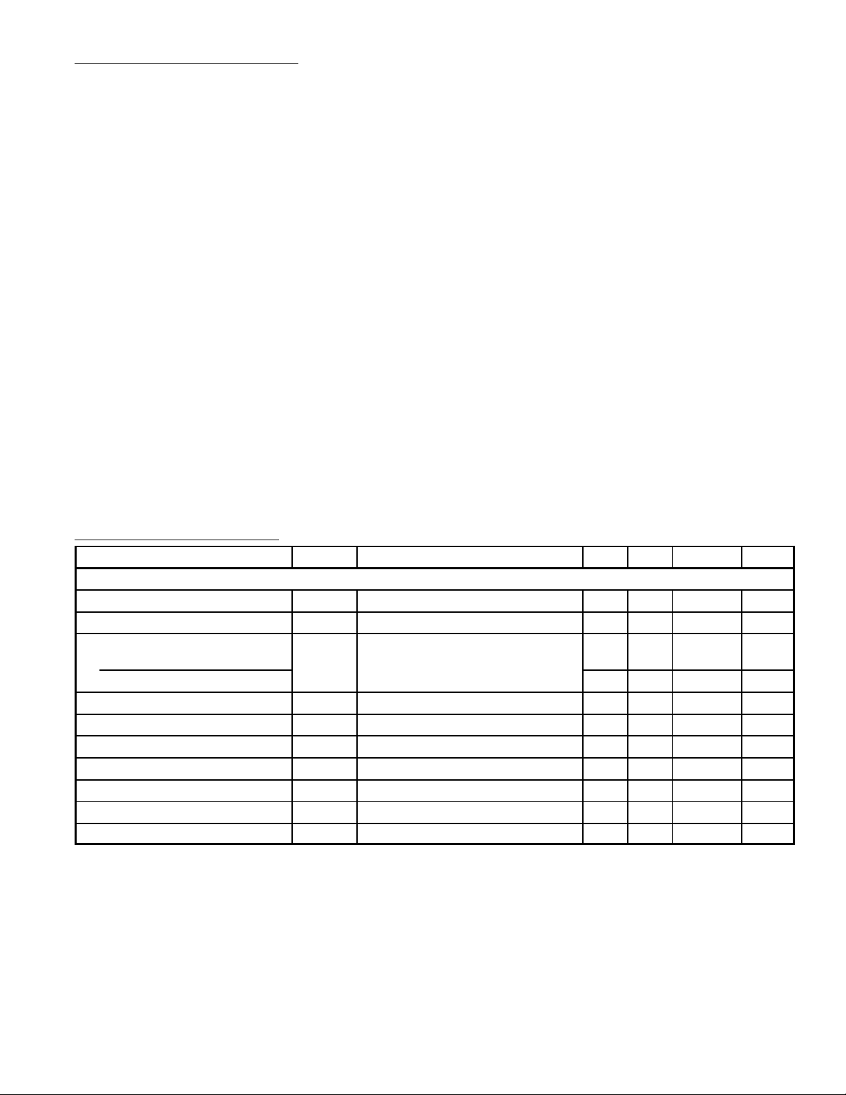
Electrical Characteristics:
Parameter Symbol Test Conditions Min Typ Max Unit
Tachometer
Input Thresholds VIN = 250mV
Hysteresis VIN = 250mV
Offset Voltage
NTE995
NTE995M – 5.0 15 mV
Input Bias Current VIN = ±50mV – 0.1 1.0 µA
Output Voltage (High Level, Pin2) V
Output Voltage (Low Level, Pin2) V
Output Current I2, I
Leakage Current I
Gain Constant K Note 3 0.9 1.0 1.1
Linearity fIN = 1kHz, 5kHz, 10kHz, Note 5 –1.0 0.3 +1.0 %
(VCC = 12V, TA = +25°C unless otherwise specified)
@ 1kHz, Note 2 ±10 ±25 ±40 mV
P–P
@ 1kHz, Note 2 – 30 – mV
P–P
OH
OL
3
VIN = 250mV
VIN = +125mV, Note 3 – 8.3 – V
VIN = –125mV, Note 3 – 2.3 – V
V2 = V3 = 6V, Note 4 140 180 240 µA
3
I2 = 0, V3 = 0 – – 0.1 µA
@ 1kHz, Note 2
P–P
– 3.5 10 mV
Note 2. Hysteresis is the sum + VTH – (–VTH), offset voltage is their difference.
Note 3. V
is equal to 3/4 x VCC – 1 VBE, VOL is equal to 1/4 x VCC – 1 VBE therefore VOH – VOL = VCC/2.
OH
The difference, V
– VOL, and the mirror gain, I2/I3, are two factors that cause the tachometer
OH
gain constant to vary from 1.0.
Note 4. Be sure when choosing the time constant R1 x C1 that R1 is such that the maximum antici-
pated output voltage at Pin3 can be reached with I
x R1. The maximum value for R1 is lim-
3
ited by the output resistance of Pin3 which is greater than 10MΩ typically.
Note 5. Nonlinearity is defined as the deviation of V
defined by the V
@ 1kHz and V
OUT
@ 10kHz. C1 = 1000pF, R1 = 68k and C2 = 0.22mFd.
OUT
(@ Pin3) for fIN = 5kHz from a straight line
OUT
 Loading...