

NTE NTE992 Datasheet
NTE992
Integrated Circuit
Quad, Single Supply Operational Amplifier
Description:
The NTE992 is an internally compensated Norton operational amplifier in a 14–Lead DIP type package designed specifically for single positive power supply applications found in industrial control systems and automotive electronics. This device contains four independent amplifiers – making it ideal
for applications such as active filters, multi–channel amplifiers, tachometers, oscillators, and other
similar usages.
Features:
D Single–Supply Operation
D Internally Compensated
D Wide Unity Gain Bandwidth: 4MHz Typ
D Low Input Bias Current: 50nA Typ
D High Open–Loop Gain: 1000V/V Min
D Large Output Voltage Swing: (V
CC
–1) V
P–P
Absolute Maximum Ratings:
Supply Voltage, V
Input Currents (I
Output Current, I
CC
+ or Iin–), I
in
O
Power Dissipation (T
in
= +25°C), P
A
D
28V. . . . . . . . . . . . . . . . . . . . . . . . . . . . . . . . . . . . . . . . . . . . . . . . . . . . . . . . . . . . . . . .
5mA. . . . . . . . . . . . . . . . . . . . . . . . . . . . . . . . . . . . . . . . . . . . . . . . . . . . . . .
50mA. . . . . . . . . . . . . . . . . . . . . . . . . . . . . . . . . . . . . . . . . . . . . . . . . . . . . . . . . . . . . . . .
625mW. . . . . . . . . . . . . . . . . . . . . . . . . . . . . . . . . . . . . . . . . . . . . .
Derate Above 25°C 5mW/°C. . . . . . . . . . . . . . . . . . . . . . . . . . . . . . . . . . . . . . . . . . . . . . . . . . . . . . .
Operating Ambient Temperature, T
Storage Temperature Range, T
Electrical Characteristics:
Parameter Symbol Test Conditions Min Typ Max Unit
Open–Loop Voltage Gain A
Input Resistance (Inverting Input) r
Output Resistance r
Input Bias Current (Inverting Input) I
(TA = +25°C, VCC = +15V unless otherwise specified)
A
stg
VOL
i
O
IB
f = 100Hz, RL = 5kΩ, Note 1 1.2 2.0 – V/mV
– 1.0 – MΩ
– 8.0 – kΩ
– 50 300 nA
–40° to +85°C. . . . . . . . . . . . . . . . . . . . . . . . . . . . . . . . . . . . . . . . .
–65° to +150°C. . . . . . . . . . . . . . . . . . . . . . . . . . . . . . . . . . . . . . . . . .
Note 1. Open–loop voltage gain is defined as voltage gain from the inverting input to the output.
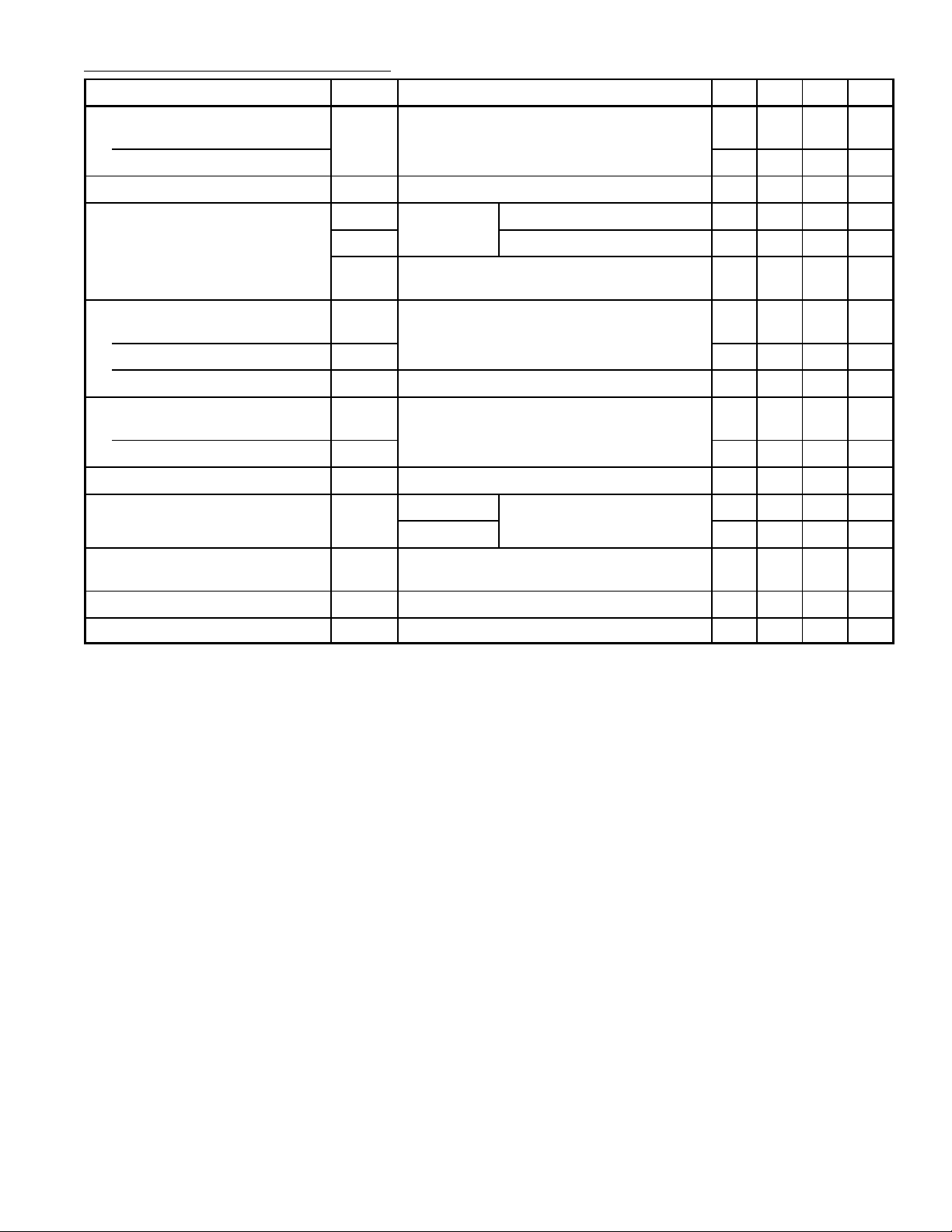
Electrical Characteristics (Cont’d): (TA = +25°C, VCC = +15V unless otherwise specified)
Parameter Symbol Test Conditions Min Typ Max Unit
Slew Rate
Positive Output Swing
Negative Output Swing – 20 – V/µs
Unity Gain Bandwidth BW – 4.0 – MHz
Output Voltage Swing (Note 6) V
Output Current
Source
Sink (Note 2) I
Low Level Output Current I
Supply Current (All Four Amps)
Non–Inverting Inputs Open
Non–Inverting Inputs Grounded I
Power Supply Rejection PSRR f = 100Hz – 55 – dB
Mirror Gain A
∆ Mirror Gain ∆Ai20µA ≤ Iin+ ≤ 200µA, TA = –40° to +85°C,
SR
OH
V
OL
V
OH
I
source
sink
OL
I
DO
DG
CL = 100pF, RL = 2kΩ – 0.5 – V/µs
V
VCC = +15V,
RL = 2kΩ
VCC = Max Rating, RL = R,
V
High (Iin– = 0, Iin+ = 0)
out
Iin– = 5µA, VOL = 1V – 5.0 – mA
Iin+ = 20µA TA = –40° to +85°C, Note 3 0.90 1.0 1.1 µA
i
Iin+ = 200µA 0.90 1.0 1.1 µA
Note 3
High (Iin– = 0, Iin+ = 0 13.5 14.2 – V
out
V
Low (Iin– = 10µA, Iin+ = 0 – 0.03 0.2 V
out
– 25.5 – V
5.0 10.0 – mA
0.5 0.87 – mA
– 6.9 10.0 mA
– 7.8 14.0 mA
– 2.0 5.0 %
Mirror Current TA = –40° to +85°C – 10 500 µA
Negative Input Current Note 5 – 1.0 – mA
Note 2. Sink current is specified for linear operation. When the device is used as a comparator (non–
linear operation) where the inverting input is overdriven, the sink current (low level output
current) capability is typically 5mA.
Note 3. This specification indicates the current gain of t he c urrent mirror which is used a s the non–
inverting input.
Note 4. Input V
match between the non–inverting and inverting inputs occurs for a mirror current
BE
(non–inverting input current) of approximately 10µA.
Note 5. Clamp transistors are included to prevent the input voltages from swinging below GND more
than approximately –0.3V. The negative input currents that may result from large signal overdrive with capacitance input coupling must be limited externally to values of approximately
1mA. Negative input currents in excess of 4mA will cause the output to drop to a low voltage.
These values apply for any one of the input terminals. If more than one of the input terminals
are simultaneously driven negative, maximum currents are reduced. Common–mode bias-
ing can be used to prevent negative input voltages.
Note 6. When used as a non–inverting amplifier, the minimum output voltage is the V
of the invert-
BE
ing input transistor.
 Loading...