

NTE NTE99 Datasheet

NTE99
Silicon NPN Transistor
w
Darlington
Description:
The NTE99 is a silicon NPN Darlington transistor in a TO3 type package designed for high–voltage,
high–speed, power switching in inductive circuits where fall time is critical. This device is particularly
suited for line–operated switchmode applications.
Applications:
D Switching Regulators
D Motor Controls
D Inverters
D Solenoid and Relay Drivers
Features:
D Fast Turn–Off Times:
1.0µs (max) Inductive Crossover Time – 20 Amps
2.5µs (max) Inductive Storage Time – 20 Amps
D Operating Temperature Range: –65° to +200°C
/Base–Emitter Speed–up Diode
Absolute Maximum Ratings:
Collector–Emitter Voltage, V
Collector–Emitter Voltage, V
Emitter–Base Voltage, V
Collector Current, I
C
CEO
CEV
EB
Continuous 50A. . . . . . . . . . . . . . . . . . . . . . . . . . . . . . . . . . . . . . . . . . . . . . . . . . . . . . . . . . . . . . . . . .
Peak (Note 1) 75A. . . . . . . . . . . . . . . . . . . . . . . . . . . . . . . . . . . . . . . . . . . . . . . . . . . . . . . . . . . . . . . .
Base Current, I
B
Continuous 10A. . . . . . . . . . . . . . . . . . . . . . . . . . . . . . . . . . . . . . . . . . . . . . . . . . . . . . . . . . . . . . . . . .
Peak (Note 1) 15A. . . . . . . . . . . . . . . . . . . . . . . . . . . . . . . . . . . . . . . . . . . . . . . . . . . . . . . . . . . . . . . .
Total Power Dissipation, P
D
TC = +25°C 250W. . . . . . . . . . . . . . . . . . . . . . . . . . . . . . . . . . . . . . . . . . . . . . . . . . . . . . . . . . . . . . . .
Derate Above 25°C 1.43W/°C. . . . . . . . . . . . . . . . . . . . . . . . . . . . . . . . . . . . . . . . . . . . . . . . . . . . . .
T
= +100°C 143W. . . . . . . . . . . . . . . . . . . . . . . . . . . . . . . . . . . . . . . . . . . . . . . . . . . . . . . . . . . . . . .
C
Operating Junction Temperature Range, T
Storage Temperature Range, T
stg
Thermal Resistance, Junction–to–Case, R
J
thJC
Maximum Lead Temperature (During Soldering, 1/8” from case for 5sec), T
Note 1. Pulse Test: Pulse Width = 5ms, Duty Cycle ≤ 10%.
400V. . . . . . . . . . . . . . . . . . . . . . . . . . . . . . . . . . . . . . . . . . . . . . . . . . . . .
600V. . . . . . . . . . . . . . . . . . . . . . . . . . . . . . . . . . . . . . . . . . . . . . . . . . . . .
8V. . . . . . . . . . . . . . . . . . . . . . . . . . . . . . . . . . . . . . . . . . . . . . . . . . . . . . . . . . .
–65° to +200°C. . . . . . . . . . . . . . . . . . . . . . . . . . . . . . . . . .
–65° to +200°C. . . . . . . . . . . . . . . . . . . . . . . . . . . . . . . . . . . . . . . . . .
0.7°C/W. . . . . . . . . . . . . . . . . . . . . . . . . . . . . . . . . . . . .
L
+275°C. . . . . . . . . . . .
Electrical Characteristics: (TC = +25°C unless otherwise specified)
µ
Parameter Symbol Test Conditions Min Typ Max Unit
OFF Characteristics (Note 2)
Collector–Emitter Sustaining Voltage V
Collector Cutoff Current I
Emitter Cutoff Current I
CEO(sus)IC
CEV
EBO
ON Characteristics (Note 2)
DC Current Gain h
Collector–Emitter Saturation Voltage V
Base–Emitter Saturation Voltage V
CE(sat)IC
BE(sat)IC
Diode Forward Voltage V
Dynamic Characteristic
Output Capacitance C
Switching Characteristics
Resistive Load
Delay Time t
Rise Time t
Storage Time t
Fall Time t
Inductive Load, Clamped
FE
ob
d
s
= 100mA, IB = 0, V
V
= 600V, V
CEV
BE(off)
= 400V 400 – – V
clamp
= 1.5V – – 0.25 mA
VBE = 2V, IC = 0 – – 350 mA
IC = 20A, VCE = 5V 25 – –
IC = 40A, VCE = 5V 10 – –
= 20A, IB = 1A – – 2.2 V
IC = 50A, IB = 10A – – 5.0 V
= 20A, IB = 1A – – 2.75 V
IF = 20A, Note 3 – 2.5 5.0 V
f
VCB = 10V, IE = 0, f
VCC = 250V, IC = 20A,
IB1 = 1A, V
r
tp = 25µs, Duty Cycle ≤ 2%
t = 25
BE(off)
s, Duty Cycle ≤ 2%
= 100kHz – – 750 pF
test
– 0.14 0.3 µs
= 5V,
– 0.3 1.0 µs
– 0.8 2.5 µs
f
– 0.3 1.0 µs
Storage Time t
Crossover Time t
sv
IC = 20A(pk), V
IB1 = 1A, V
c
BE(off)
clamp
= 5V
= 250V,
– 1.0 2.5 µs
– 0.36 1.0 µs
Note 2. Pulse Test: Pulse Widtg = 300µs, Duty Cycle ≤ 2%.
Note 3. The internal Collector–to–Emitter diode can eliminate the need for an external diode to
clamp inductive loads. Tests have shown that the Forward Recovery Voltage (V
) of this
f
diode is comparable to that of typical fast recovery rectifiers.
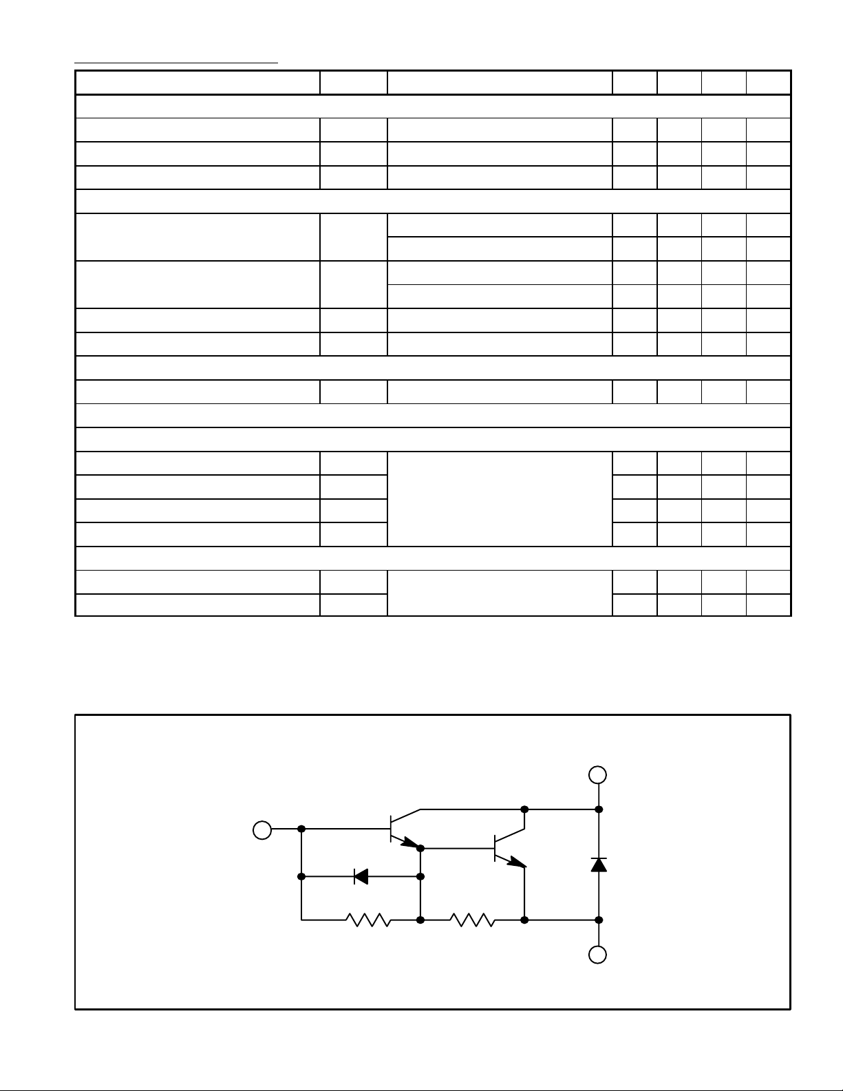
Circuit Outline
C
B
[ 50 [ 8
E
 Loading...