

NTE NTE989 Datasheet

NTE989
Integrated Circuit
General Purpose Phase Lock Loop (PLL)
Description:
The NTE989 is a general purpose Phase Locked Loop (PLL) in a 14–Lead DIP type package containing a stable, highly linear voltage controlled oscillator for low distortion FM demodulation, and a
double balanced phase detector with good carrier suppression. The VCO frequency is set with an
external resistor and capacitor, and tuning range of 10:1 can be obtained with the same capacitor.
The characteristics of the closed loop system–bandwidth, response speed, capture and pull in range–
may be adjusted over a wide range with an external resistor and capacitor. The loop may be broken
between the VCO and the phase detector for insertion of a digital frequency divider to obtain frequency multiplication.
Features:
D 200ppm/°C frequency stability of the VCO
D Power supply range of ±5 to ±12 volts with 100ppm/% typical
D 0.2% linearity of demodulated output
D Linear triangle wave with in phase zero crossings available
D TTL and DTL compatible phase detector input and square wave output
D Adjustable hold in range from ±1% to > ±60%
Applications:
D Data and tape synchronization
D Modems
D FSK demodulation
D FM demodulation
D Frequency synthesizer
D Tone decoding
Absolute Maximum Ratings:
Supply Voltage ±12V. . . . . . . . . . . . . . . . . . . . . . . . . . . . . . . . . . . . . . . . . . . . . . . . . . . . . . . . . . . . . . . . . . . .
Power Dissipation (Note 1) 300mW. . . . . . . . . . . . . . . . . . . . . . . . . . . . . . . . . . . . . . . . . . . . . . . . . . . . . .
Differential Input Voltage ±1V. . . . . . . . . . . . . . . . . . . . . . . . . . . . . . . . . . . . . . . . . . . . . . . . . . . . . . . . . . . .
Operating Temperature Range 0°C to +70°C. . . . . . . . . . . . . . . . . . . . . . . . . . . . . . . . . . . . . . . . . . . . . . .
Storage Temperature Range –65°C to +150°C. . . . . . . . . . . . . . . . . . . . . . . . . . . . . . . . . . . . . . . . . . . . .
Lead Temperature (Soldering, 10 sec) +300°C. . . . . . . . . . . . . . . . . . . . . . . . . . . . . . . . . . . . . . . . . . . . .
D Frequency multiplication and division
D SCA demodulators
D Telemetry receivers
D Signal regeneration
D Coherent demodulators
Note 1. The maximum junction temperature of the NTE989 is 100°C. Thermal resistance for this
device is 100°C/W.
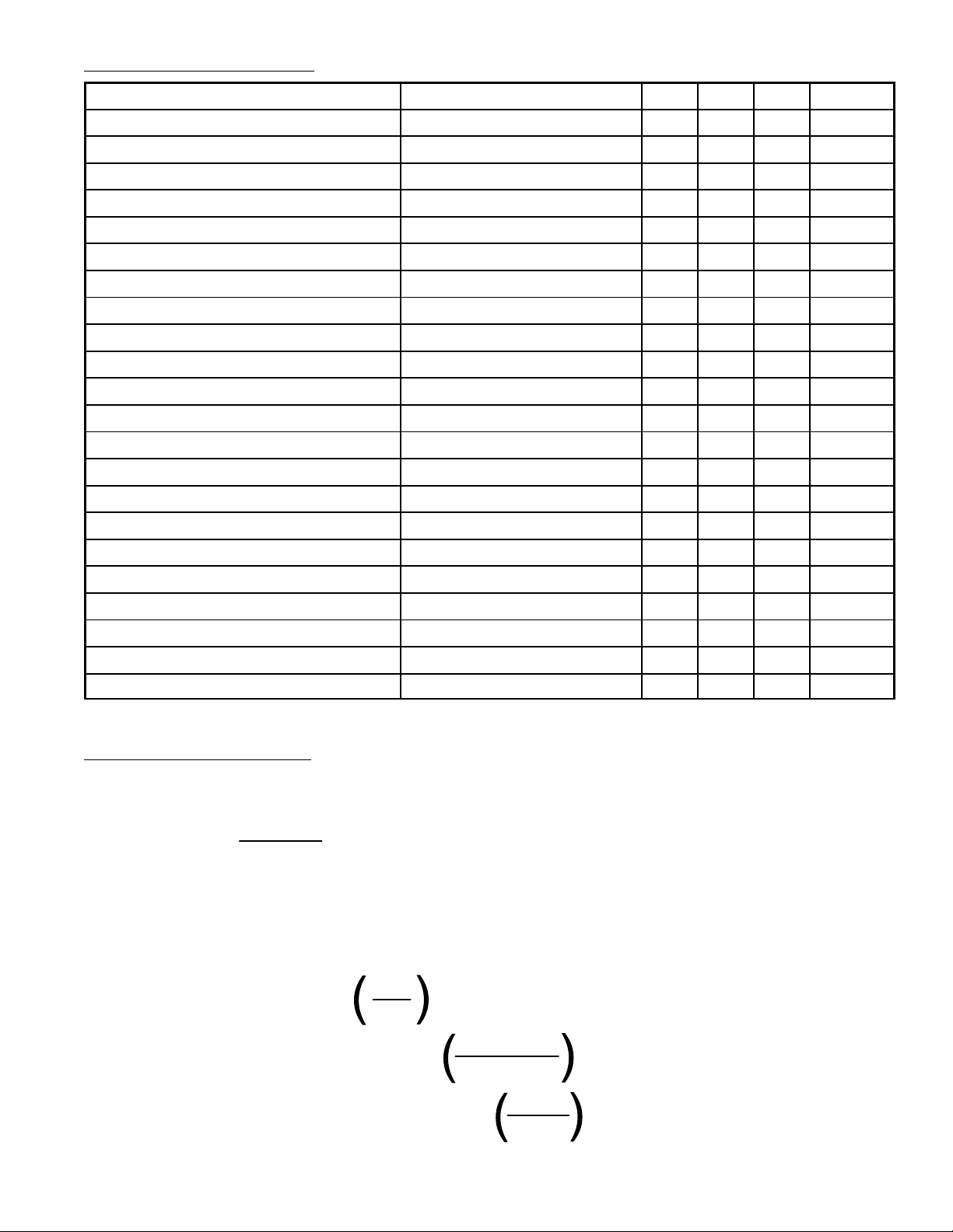
Electrical Characteristics: (TA = +25°C, VC = ±6V unless otherwise specified)
Parameter Conditions Min Typ Max Unit
Power Supply Current – 8.0 12.5 mA
Input Impedance (Pins 2,3) –4V < V2, V3 < 0V – 5 – kΩ
VCO Maximum Operating Frequency Co = 2.7pF 250 500 – kHz
Operating Frequency Temperature Coefficient – –200 500 ppm/°C
Frequency Drift with Supply Voltage – 0.05 0.2 %/V
Triangle Wave Output Voltage 2 2.4 3 V
Triangle Wave Output Linearity – 0.5 1 %
Square Wave Output Level 4.7 5.4 – V
Output Impedance (Pin 4) – 5 – kΩ
Square Wave Duty Cycle 40 50 60 %
Square Wave Rise Time – 20 – ns
Square Wave Fall Time – 50 – ns
Output Current Sink (Pin 4) 0.6 1 – mA
VCO Sensitivity fo = 10kH
Demodulated Output Voltage (Pin 7) ±10% Frequency Deviation 200 300 400 mV
Total Harmonic Distortion ±10% Frequency Deviation – 0.2 1.5 %
Output Impedance (Pin 7) – 3.5 – kΩ
DC Level (Pin 7) 4.0 4.5 5.0 V
Output Offset Voltage |V7 – V6| – 50 200 mV
Temperature Drift of |V7 – V6| – 500 – µV/°C
AM Rejection – 40 – dB
Phase Detector Sensitivity K
D
Z
6000 6600 7200 HZ/V
0.55 .68 0.95 V/radian
p–p
p–p
pp
Applications Information:
In designing with phase locked loops the important parameters of interest are:
FREE RUNNING FREQUENCY
1
≅
f
o
3.7 R
0C0
LOOP GAIN:
The Loop Gain relates the amount of phase change between the input signal and the VCO signal for a shift in input signal frequency (assuming the loop remains in lock). In servo theory,
this is called the “velocity error coefficient”.
1
Loop gain = KoK
D
sec
radians/sec
Ko = oscillator sensitivity
volt
volts
KD = phase detector sensitivity
radian
 Loading...