

NTE NTE984 Datasheet

NTE984
Integrated Circuit
TV Video IF System
Description:
The NTE984 is a monolithic integrated circuit in a 16–Lead DIP type package designed to perform
IF amplification, video d etection, a nd v i deo–amplifier f unctions i n c olor a nd m onochrome T V r eceivers.
Features:
D Improved AGC, Fast Response, Sample and Hold Keyed
D High Gain Wideband IF Amplifiers
D Delayed AGC Output for Tuner
D Gain Reduction with Excellent Stability
D Linear Video Detector
D Video Amplifier
D Low Noise
D Internal Shunt Regulator
D For Color of Monochrome
Absolute Maximum Ratings:
DC Supply Voltage:
Between Pin15 and Pin4 16V. . . . . . . . . . . . . . . . . . . . . . . . . . . . . . . . . . . . . . . . . . . . . . . . . . . . . .
Between 470Ω Connected to Pin12 and Pin14 35V. . . . . . . . . . . . . . . . . . . . . . . . . . . . . . . . . . .
DC Supply Current:
At Pin15 20mA. . . . . . . . . . . . . . . . . . . . . . . . . . . . . . . . . . . . . . . . . . . . . . . . . . . . . . . . . . . . . . . . . .
At Pin12 30mA. . . . . . . . . . . . . . . . . . . . . . . . . . . . . . . . . . . . . . . . . . . . . . . . . . . . . . . . . . . . . . . . . .
Device Dissipation (T
≤ +55°C), P
A
D
Derate Linearly Above +55°C 7.9mW/°C. . . . . . . . . . . . . . . . . . . . . . . . . . . . . . . . . . . . . . . . . . .
Operating Ambient Temperature Range, T
Storage Temperature Range, T
stg
A
Lead Temperature (During Soldering, 1/16” ±1/32” from case, 10sec max), T
750mW. . . . . . . . . . . . . . . . . . . . . . . . . . . . . . . . . . . . . . . . . . . . . .
–40° to +85°C. . . . . . . . . . . . . . . . . . . . . . . . . . . . . . . . . . .
–65° to +150°C. . . . . . . . . . . . . . . . . . . . . . . . . . . . . . . . . . . . . . . . . .
L
+265°C. . . . . . . . . . .
Electrical Characteristics: (TA = +25°C unless otherwise specified)
Parameter Symbol Test Conditions Min Typ Max Unit
Operating Supply Voltage V
Supply Current I
Shunt Regulator Voltage V
Shunt Regulator Current I
Tuner AGC High Voltage V
Tuner AGC Low Voltage V
AGC Current I
AGC Peak Current I
Horizontal Key Input Through 100kΩ connected to Pin1 25 – 35 V
Video Output High Voltage V
Video Output Low Voltage V
Sensitivity Voltage V
Noise – – 12 mV
Chroma 45.75MHz, 10mV; 42.17MHz, 3mV 0.7 – 1.6 V
AFT Drive 35 – 85 mV
Distortion 50kHz, 80% Modulated,
Delay Voltage Through 15kΩ connected to Pin7,
Note 1 12.0 – 14.2 V
15
15
12
V12 = 10.5V 6 – 20 mA
12
10
10
Non–Keyed 80 – 500 µA
2
Keyed Source Current 0.7 – 3.0 mA
2
Keyed Sink Current 150 – 680 µA
At Zero Carrier 7 – 10 V
16
At 30mV Input 0.9 – 2.0 V
16
At 400µV Input 0.9 – 5.0 V
16
Sync Tip Equiv. 30mV
Note 2
rms
3 – 15 mA
10.9 – 13.0 V
18.5 – 21.0 V
0.3 – 1.3 V
– – 10 %
0 – V
15
rms
rms
rms
V
Note 1 V15 Min should be at least 0.6V above Terminal 12 potential. Lower voltage may cause some
“white” compression.
Note 2 Zero voltage corresponds to maximum delay at signal input + 30mV
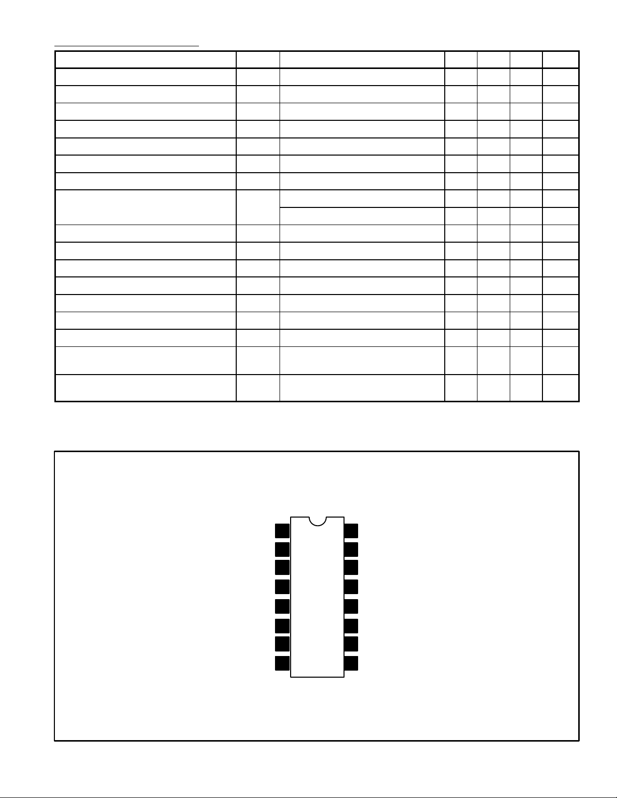
Pin Connection Diagram
Key Pulse Input
AGC Filter
A1 Input
GND
Clamp Capacitor
A1 Output/A2 Input
AGC Delay
IF AGC Bias
1
2
3
4
5
6
7
8
Video Output
16
15
(+) V
Substrate
14
13
Detector Bias
12
(+) V
11
A3 Input and Detector
10
Tuner AGC
9
A2 Output
2
S
1 Shunt Reg
S
(RMS)
.
 Loading...