

NTE NTE983 Datasheet
NTE983
Integrated Circuit
Low Noise Dual Preamp
Description:
The NTE983 is a linear monolithic integrated circuit in a 14–Lead DIP type package designed for use
with low–level signals in low–noise applications. This device offers outstanding value, performance,
and reliability in both consumer and industrial products such as stereo tape players, microphone
amplif i e rs, phonograph preamplifiers, and FM stereo receivers.
An i ntegral v oltage r egulator e lim inates the n eed f or a udio o r R F d ecoupling. Internal f eedback r esi stors
are provided for NAB equalization.
Features:
D Single Power Supply Operation
D Wide Supply Voltage Range
D Matched Open Loop Voltage Gain
D Turn–On Delay
Absolute Maximum Ratings:
Power Supply, V
Power Dissipation, P
CC
D
Derate Above 25°C 8.3mW/°C. . . . . . . . . . . . . . . . . . . . . . . . . . . . . . . . . . . . . . . . . . . . . . . . . . . . .
Operating Temperature Range, T
Storage Temperature Range, T
stg
opr
–20° to +85°C. . . . . . . . . . . . . . . . . . . . . . . . . . . . . . . . . . . . . . . . .
–65° to +150°C. . . . . . . . . . . . . . . . . . . . . . . . . . . . . . . . . . . . . . . . . .
+16V. . . . . . . . . . . . . . . . . . . . . . . . . . . . . . . . . . . . . . . . . . . . . . . . . . . . . . . . . . . . . . . .
670mW. . . . . . . . . . . . . . . . . . . . . . . . . . . . . . . . . . . . . . . . . . . . . . . . . . . . . . . . . . .
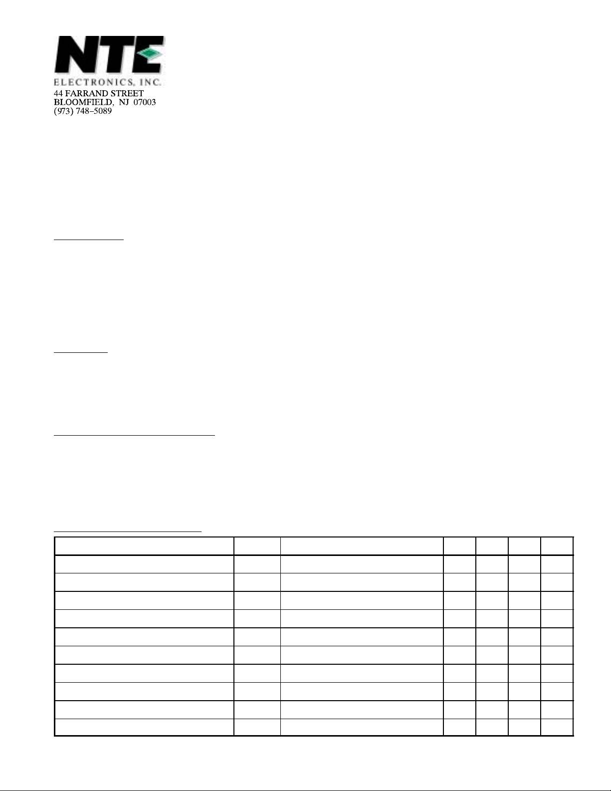
Electrical Characteristics: (TA = +25°C, +10.5V ≤ VCC +16V unless otherwise noted)
Parameter Symbol Test Conditions Min Typ Max Unit
Voltage Gain G
Total Harmonic Distortion THD f = 1kHz, V
Noise Out RS = 620Ω – 1.5 – mV
Gain Balance – – 2.0 dB
Channel Separation Sep 40 – – kΩ
Input Impedance z
Ripple Rejection RR f = 1kHz – 35 – dB
Input Bias Current I
Turn–On Delay t
Supply Current I
CC
f = 1kHz 40 – 46 dB
V
= 500mV
out
i
B
d
rms
– 0.5 1.0 %
– 40 – kΩ
– – 3.0 µA
– 1.0 – sec
– – 12 mA
Pin Connection Diagram
GND 1
Feedback A
Input A
Input A
Output A
Output A1
Delay A
2
3
4
5
6
7
14 8
Feedback B
14
Input B
13
Bias
12
Output B
11
Output B1
10
Delay B
9
8
V
CC
17
.785 (19.95) Max
.300 (7.62)
.200
(5.08)
Max
.100 (2.45) .099 (2.5) Min
.600 (15.24)
 Loading...